

Ultrafast SiGe
www.BDTIC.com/ADI
FEATURES
95 ps propagation delay
7.5 GHz toggle rate
60 ps typical output rise/fall
60 fs random jitter (RJ)
On-chip terminations at both input pins
Extended industrial temperature range: −40°C to +125°C
2.5 V to 3.3 V power supply (V
APPLICATIONS
Clock and data signal restoration and level shifting
Automated test equipment (ATE)
High speed instrumentation
High speed line receivers
Threshold detection
Converter clocking
GENERAL DESCRIPTION
The ADCLK905 (one input, one output), ADCLK907 (dual one
input, one output), and ADCLK925 (one input, two outputs) are
ultrafast clock/data buffers fabricated on the Analog Devices, Inc.,
proprietary XFCB3 silicon germanium (SiGe) bipolar process.
The ADCLK905/ADCLK907/ADCLK925 feature full-swing
emi
tter coupled logic (ECL) output drivers. For PECL (positive
ECL) operation, bias V
For NECL (negative ECL) operation, bias V
V
to the negative supply.
EE
The buffers offer 95 ps propagation delay, 7.5 GHz toggle rate,
ps data rate, and 60 fs random jitter (RJ).
10 Gb
The inputs have center tapped, 100 Ω, on-chip termination
r
esistors. A V
REF
The ECL output stages are designed to directly drive 800 mV
ach side into 50 Ω terminated to V
e
differential output swing of 1.6 V.
The ADCLK905/ADCLK907/ADCLK925 are available in
16-lead LFCS
P packages.
to the positive supply and VEE to ground.
CC
pin is available for biasing ac-coupled inputs.
− VEE)
CC
− 2 V for a total
CC
to ground and
CC
ECL Clock/Data Buffers
ADCLK905/ADCLK907/ADCLK925
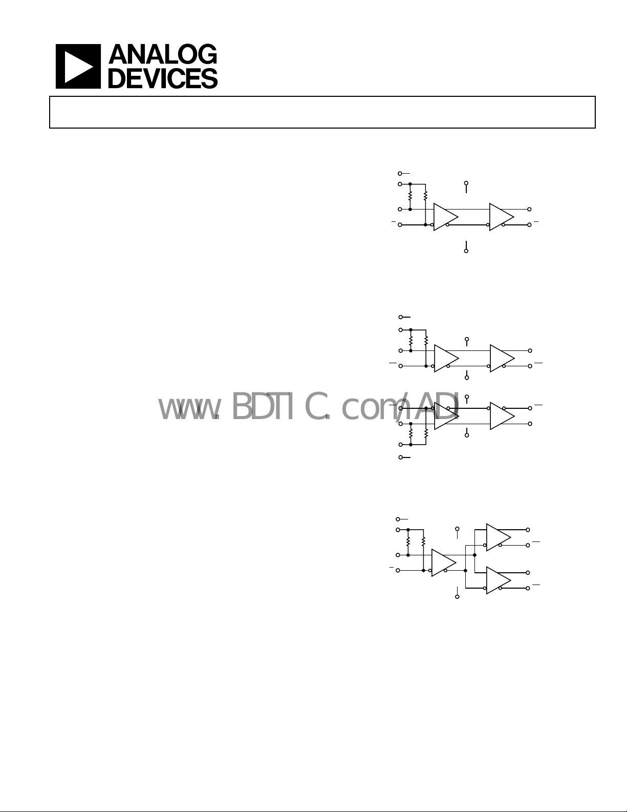
TYPICAL APPLICATION CIRCUITS
V
REF
V
T
D
D
Figure 1. ADCLK905 ECL 1:1 Clock/Data Buffer
V
1
REF
VT1
D1
D1
D2
D2
VT2
V
2
REF
Figure 2. ADCLK907 ECL Dual 1:1 Clock/Data Buffer
V
REF
V
T
D
D
Figure 3. ADCLK925 ECL 1:2 Clock/Data Fanout Buffer
V
CC
Q
Q
V
EE
V
CC
V
EE
V
EE
V
CC
V
CC
V
EE
Q1
Q1
Q2
Q2
Q1
Q1
Q2
Q2
06318-001
06318-002
06318-003
Rev. 0
Information furnished by Analog Devices is believed to be accurate and reliable. However, no
responsibility is assumed by Anal og Devices for its use, nor for any infringements of patents or ot her
rights of third parties that may result from its use. Specifications subject to change without notice. No
license is granted by implication or otherwise under any patent or patent rights of Analog Devices.
Trademarks and registered trademarks are the property of their respective owners.
One Technology Way, P.O. Box 9106, Norwood, MA 02062-9106, U.S.A.
Tel: 781.329.4700 www.analog.com
Fax: 781.461.3113 ©2007 Analog Devices, Inc. All rights reserved.

ADCLK905/ADCLK907/ADCLK925
www.BDTIC.com/ADI
TABLE OF CONTENTS
Features.............................................................................................. 1
Applications....................................................................................... 1
General Description ......................................................................... 1
Typical Application Circuits........................................................... 1
Revision History ............................................................................... 2
Specifications..................................................................................... 3
Electrical Characteristics ............................................................. 3
Absolute Maximum Ratings............................................................ 5
Thermal Resistance ...................................................................... 5
ESD Caution.................................................................................. 5
Pin Configurations and Function Descriptions ........................... 6
REVISION HISTORY
8/07—Revision 0: Initial Version
Typical Performance Characteristics..............................................8
Applications Information.............................................................. 11
Power/Ground Layout and Bypassing..................................... 11
Output Stages............................................................................... 11
Optimizing High Speed Performance..................................... 11
Buffer Random Jitter.................................................................. 11
Typical Application Circuits ......................................................... 12
Evaluation Board Schematic......................................................... 13
Outline Dimensions....................................................................... 14
Ordering Guide .......................................................................... 14
Rev. 0 | Page 2 of 16
ADCLK905/ADCLK907/ADCLK925
www.BDTIC.com/ADI
SPECIFICATIONS
ELECTRICAL CHARACTERISTICS
Typical (Typ) values are given for VCC − VEE = 3.3 V and TA = 25°C, unless otherwise noted. Minimum (Min) and maximum (Max) values are
given over the full V
Table 1.
Parameter Symbol Min Typ Max Unit Conditions
DC INPUT CHARACTERISTICS
Input Voltage High Level VIH V
Input Voltage Low Level VIL V
Input Differential Range VID 0.2 3.4 V p-p −40°C to +85°C
V
Input Capacitance CIN 0.4 pF
Input Resistance, Single-Ended Mode 50 Ω
Input Resistance, Differential Mode 100 Ω
Input Resistance, Common Mode 50 kΩ Open VT
Input Bias Current 20 μA
DC OUTPUT CHARACTERISTICS
Output Voltage High Level VOH V
Output Voltage Low Level VOL V
Output Voltage Differential VOD 610 1040 mV 50 Ω to (VCC − 2.0 V)
Reference Voltage V
Output Voltage (VCC + 1)/2 V −500 μA to +500 μA
Output Resistance 250 Ω
AC PERFORMANCE
Propagation Delay tPD 70 95 125 ps VCC = 3.3 V ± 10%,
70 95 125 ps VCC = 2.5 V ± 5%,
Propagation Delay Temperature Coefficient 50 fs/°C
Propagation Delay Skew (Output to Output)
ADCLK907
Propagation Delay Skew (Output to Output)
ADCLK925
Propagation Delay Skew (Device to Device) 35 ps VID = 0.5 V
Toggle Rate 6 7.5 GHz >0.8 V differential output swing,
6.5 GHz >0.8 V differential output swing,
Random Jitter RJ 60 fs rms VID = 1600 mV, 8 V/ns, V
Rise/Fall Time tR/tF 30 85 ps 20%/80%
Additive Phase Noise
622.08 MHz −138 dBc/Hz @10 Hz offset
−144 dBc/Hz @100 Hz offset
−152 dBc/Hz @1 kHz offset
−159 dBc/Hz @10 kHz offset
−161 dBc/Hz @100 kHz offset
−161 dBc/Hz >1 MHz offset
122.88 MHz −135 dBc/Hz @10 Hz offset
−145 dBc/Hz @100 Hz offset
−153 dBc/Hz @1 kHz offset
−160 dBc/Hz @10 kHz offset
−161 dBc/Hz @100 kHz offset
−161 dBc/Hz >1 MHz offset
− VEE = 3.3 V ± 10% and TA = −40°C to +125°C variation, unless otherwise noted.
CC
+ 1.6 VCC V
EE
V
EE
0.2 2.8 V p-p 85°C to 125°C
ID
− 1.26 VCC − 0.76 V 50 Ω to (VCC − 2.0 V)
CC
− 1.99 VCC − 1.54 V 50 Ω to (VCC − 2.0 V)
CC
REF
− 0.7 V
CC
15 ps VID = 0.5 V
10 ps VID = 0.5 V
(±1.7 V between input pins)
(±1.4 V between input pins)
V
= V
, VID = 0.5 V p-p
ICM
REF
V
= V
ICM
V
CC
V
CC
, VID = 0.5 V p-p
REF
= 3.3 V ± 10%
= 2.5 V ± 5%
= 1.85 V
ICM
Rev. 0 | Page 3 of 16
ADCLK905/ADCLK907/ADCLK925
www.BDTIC.com/ADI
Parameter Symbol Min Typ Max Unit Conditions
POWER SUPPLY
Supply Voltage Requirement VCC − VEE 2.375 3.63 V 2.5 V − 5% to 3.3 V + 10%
Power Supply Current Static
ADCLK905
Negative Supply Current I
25 40 mA
Positive Supply Current I
48 63 mA
ADCLK907
Negative Supply Current I
50 80 mA
Positive Supply Current I
96 126 mA
ADCLK925
Negative Supply Current I
31 51 mA
Positive Supply Current I
77 97 mA
Power Supply Rejection
Output Swing Supply Rejection
1
Change in TPD per change in VCC.
2
Change in output swing per change in VCC.
1
2
24 mA VCC − VEE = 2.5 V
VEE
V
− VEE = 3.3 V ± 10%
CC
47 mA VCC − VEE = 2.5 V
VCC
V
− VEE = 3.3 V ± 10%
CC
48 mA VCC − VEE = 2.5 V
VEE
V
− VEE = 3.3 V ± 10%
CC
94 mA VCC − VEE = 2.5 V
VCC
V
− VEE = 3.3 V ± 10%
CC
29 mA VCC − VEE = 2.5 V
VEE
V
− VEE = 3.3 V ± 10%
CC
76 mA VCC − VEE = 2.5 V
VCC
V
− VEE = 3.3 V ± 10%
CC
PSR
3 ps/V VCC − VEE = 3.0 V ± 20%
VCC
PSR
26 dB VCC − VEE = 3.0 V ± 20%
VCC
Rev. 0 | Page 4 of 16
ADCLK905/ADCLK907/ADCLK925
www.BDTIC.com/ADI
ABSOLUTE MAXIMUM RATINGS
Table 2.
Parameter Rating
Supply Voltage
VCC − VEE 6.0 V
Input Voltage
D (D1, D2), D (D1, D2)
D1, D2, D1, D2 to VT Pin
(CML or PECL Termination)
D (D1, D2) to D (D1, D2)
Maximum Voltage on Output Pins VCC + 0.5 V
Maximum Output Current 35 mA
Input Termination, VT to D (D1, D2), D (D1, D2)
Voltage Reference, V
Temperature
Operating Temperature Range, Ambient −40°C to +125°C
Operating Temperature, Junction 150°C
Storage Temperature Range −65°C to +150°C
Stresses above those listed under Absolute Maximum Ratings
may cause permanent damage to the device. This is a stress
rating only; functional operation of the device at these or any
other conditions above those indicated in the operational
section of this specification is not implied. Exposure to absolute
maximum rating conditions for extended periods may affect
device reliability.
V
REF
V
− 0.5 V to
EE
+ 0.5 V
V
CC
±40 mA
±1.8 V
±2 V
− VEE
CC
THERMAL RESISTANCE
θJA is specified for the worst-case conditions, that is, a device
soldered in a circuit board for surface-mount packages.
Table 3. Thermal Resistance
Package Type θJA Unit
16-lead LFCSP 70 °C/W
ESD CAUTION
Rev. 0 | Page 5 of 16

ADCLK905/ADCLK907/ADCLK925
V
www.BDTIC.com/ADI
PIN CONFIGURATIONS AND FUNCTION DESCRIPTIONS
REF
T
EE
CC
V
V
V
V
14
13
15
16
PIN 1
1D
2D
ADCLK905
3NC
(Not to Scale)
4NC
INDICAT OR
TOP VIEW
12 Q
11 Q
10 NC
9NC
NC = NO CONNECT
5
6
NC
NC
Figure 4. ADCLK905 Pin Configuration
Table 4. Pin Function Descriptions for 1:1 ADCLK905 Buffer
Pin No. Mnemonic Description
1 D Noninverting Input.
2
3, 4, 5, 6,
D
NC No Connect. No physical connection to the die.
Inverting Input.
9, 10
7, 14 VEE Negative Supply Voltage.
8, 13 VCC Positive Supply Voltage.
11
Q
Inverting Output.
12 Q Noninverting Output.
15 V
Reference Voltage. Reference voltage for biasing ac-coupled inputs.
REF
16 VT Center Tap. Center tap of 100 Ω input resistor.
Heat Sink NC
No Connect. The metallic back surface of the package is not elec
It can be left floating for optimal electrical isolation between the package handle and the substrate of the die.
It can also be soldered to the application board if improved thermal and/or mechanical stability is desired.
Exposed metal at the corners of the package is connected to this back surface. Allow sufficient clearance
to vias and other components.
1
1
REF
T
EE
V
V
V
V
13
14
15
16
PIN 1
INDICATO R
1D1
2D1
ADCLK907
3D2
TOP VIEW
(Not to Scale)
4D2
8
7
EE
CC
V
06318-004
trically connected to any part of the circuit.
CC
12 Q1
11 Q1
10 Q2
9Q2
7
5
6
2
2
T
F
V
V
RE
Figure 5. ADCLK907 Pin Configuration
Table 5. Pin Function Descriptions for Dual 1:1 ADCLK907 Buffer
Pin No. Mnemonic Description
1 D1 Noninverting Input 1.
2
D1
Inverting Input 1.
3 D2 Noninverting Input 2.
4
D2
Inverting Input 2.
5 VT2 Center Tap 2. Center tap of 100 Ω input resistor, Channel 2.
6 V
REF
2
Reference Voltage 2. Reference voltage for biasing ac-coupled inputs, Channel 2.
7, 14 VEE Negative Supply Voltage.
8, 13 VCC Positive Supply Voltage. Pin 8 and Pin 13 are not strapped internally.
9
Q2
Inverting Output 2.
Rev. 0 | Page 6 of 16
8
EE
CC
V
06318-005

ADCLK905/ADCLK907/ADCLK925
www.BDTIC.com/ADI
Pin No. Mnemonic Description
10 Q2 Noninverting Output 2.
11
Q1
12 Q1 Noninverting Output 1.
15 V
1 Reference Voltage 1. Reference voltage for biasing ac-coupled inputs, Channel 1.
REF
16 VT1 Center Tap 1. Center tap of 100 Ω input resistor, Channel 1.
Heat Sink NC
Inverting Output 1.
No Connect. The metallic back surface of the package is not elec
trically connected to any part of the circuit.
It can be left floating for optimal electrical isolation between the package handle and the substrate of the die.
It can also be soldered to the application board if improved thermal and/or mechanical stability is desired.
Exposed metal at the corners of the package is connected to this back surface. Allow sufficient clearance
to vias and other components.
REF
T
EE
CC
V
V
V
V
14
13
15
16
PIN 1
1D
2D
ADCLK925
3NC
(Not to Scale)
4NC
INDICAT OR
TOP VIEW
12 Q1
11 Q1
10 Q2
9Q2
NC = NO CONNECT
5
6
NC
NC
Figure 6. ADCLK925 Pin Configuration
Table 6. Pin Function Descriptions for 1:2 ADCLK925 Buffer
Pin No. Mnemonic Description
1 D Noninverting Input.
2
D
Inverting Input.
3, 4, 5, 6 NC No Connect. No physical connection to the die.
7, 14 VEE Negative Supply Voltage.
8, 13 VCC Positive Supply Voltage.
9
Q2
Inverting Output 2.
10 Q2 Noninverting Output 2.
11
Q1
Inverting Output 1.
12 Q1 Noninverting Output 1.
15 V
Reference Voltage. Reference voltage for biasing ac-coupled inputs.
REF
16 VT Center Tap. Center tap of 100 Ω input resistor.
Heat Sink NC
No Connect. The metallic back surface of the package is not elec
It can be left floating for optimal electrical isolation between the package handle and the substrate of the die.
It can also be soldered to the application board if improved thermal and/or mechanical stability is desired.
Exposed metal at the corners of the package is connected to this back surface. Allow sufficient clearance
to vias and other components.
8
7
EE
CC
V
V
06318-006
trically connected to any part of the circuit.
Rev. 0 | Page 7 of 16

ADCLK905/ADCLK907/ADCLK925
V
–
–
V
–
www.BDTIC.com/ADI
TYPICAL PERFORMANCE CHARACTERISTICS
VCC = 3.3 V, VEE = 0.0 V, TA = 25°C, outputs terminated 50 Ω to VCC − 2 V, unless otherwise noted.
2.37V
Q
100mV/DI
Q
1.37V
200ps/DIV
Figure 7. Output Waveform, V
90
AGILENT E5500
CARRIER: 122.88MHz
NO SPURS
–100
–110
–120
–130
L[f] (dBc/Hz)
–140
–150
–160
–170
10 100 1k 10k 100k 1M 10M 100M
f (Hz)
= 3.3 V
CC
Figure 8. Phase Noise at 122.88 MHz
2.37V
Q
100mV/DI
Q
06318-007
06318-008
1.37V
100ps/DIV
Figure 10. Output Waveform, V
90
AGILENT E5500
CARRIER: 622.08MHz
NO SPURS
–100
–110
–120
–130
L[f] (dBc/Hz)
–140
–150
–160
–170
10 100 1k 10k 100k 1M 10M 100M
f (Hz)
= 3.3 V
CC
06318-010
06318-011
Figure 11. Phase Noise at 622.08 MHz
90
AGILENT E5500
CARRIER: 245.76MHz
–100
NO SPURS
–110
–120
–130
L[f] (dBc/Hz)
–140
–150
–160
–170
10 100 1k 10k 100k 1M 10M 100M
f (Hz)
6318-009
Figure 9. Phase Noise at 245.76 MHz
Rev. 0 | Page 8 of 16
300
250
200
150
RMS JITT ER (fs)
100
50
0
012345678
INPUT SLEW RATE ( V/ns)
Figure 12. RMS Jitter vs. Input Slew Rate
6318-012

ADCLK905/ADCLK907/ADCLK925
www.BDTIC.com/ADI
1.1
1.0
0.9
0.8
0.7
OUTPUT SWING (V)
0.6
0.5
0.4
1234
+125°C
+25°C
Figure 13. V
–55°C
SUPPLY VOLTAGE (V)
vs. Power Supply Voltage
OD
6318-013
0.09
0.08
0.07
0.06
0.05
0.04
0.03
0.02
POWER SUPPLY CURRENT (A)
0.01
0
01234
+25°C
+25°C
SUPPLY VOLTAGE (V)
+125°C
–55°C
+125°C
–55°C
Figure 16. Power Supply Current vs. Supply Voltage, ADCLK925
06318-016
0.07
0.06
0.05
0.04
0.03
0.02
POWER SUPPLY CURRENT (A)
0.01
0
+25°C
+125°C
+25°C
–55°C
POWER SUPPLY VOLTAGE (V)
+125°C
–55°C
3.0 3.52.5 4.0
Figure 14. Power Supply Current vs. Power Supply Voltage, ADCLK905
110
105
(ps)
100
95
PROPAGATION DELAY
90
1.6 2.1 2.6 3.1 3.6
INPUT COMMO N MO DE ( V)
Figure 15. Propagation Delay vs. V
+125°C
+25°C
–55°C
; Input Swing = 200 mV
ICM
100
99
98
97
(ps)
PD
t
96
95
94
0.4 0.6 0.8 1.0 1.2 1.4 1.6 1.8
06318-014
Figure 17. Propagation Delay vs. V
1.8
1.6
1.4
1.2
1.0
(V)
OD
0.8
V
0.6
0.4
0.2
0
0.5
1.5
2.5
06318-015
3.5
VID (V)
4.5
5.5
6.5
FREQUENCY (G Hz )
7.5
06318-017
ID
8.5
9.5
10.5
11.5
12.5
06318-018
Figure 18. Toggle Rate, Differential Output Swing vs. Frequency
Rev. 0 | Page 9 of 16

ADCLK905/ADCLK907/ADCLK925
www.BDTIC.com/ADI
1
C4
1
C4
2
3
Figure 19. 2.488 Gbps PRBS 2
23
− 1 with OC-48/STM-16 Mask,
Measured p-p Jitter 8.1 ps, Source p-p Jitter 3.5 ps
1
C4
2
15ps/DIV
3
Figure 20. 9.95 Gbps PRBS 2
23
− 1 with OC-193/STM-64 Mask,
Measured p-p Jitter 10.5 ps, Source p-p Jitter 6.0 ps
58ps/DIV
2
17ps/DIV
06318-019
3
06318-023
Figure 22. 8.50 Gbps PRBS 223 − 1 with FC8500E ABS Beta Rx Mask,
Measured p-p Jitter 10.9 ps, Source p-p Jitter 4.4 ps
1
C4
2
58ps/DIV
06318-022
Figure 23. 2.5 Gbps PRBS 2
3
23
− 1 with PCI Express 2.5 Rx Mask,
06318-021
Measured p-p Jitter 8.1 ps, Source p-p Jitter 3.5 ps
Figure 21. 4.25 Gbps PRBS 2
Measured p-p Jitter 8.2 ps, Source p-p Jitter 3.4 ps
1
C4
2
34ps/DIV
3
23
− 1 with FC4250 (Optical) Mask,
06318-020
Figure 24. 5.0 Gbps PRBS 2
1
C4
2
29ps/DIV
3
23
− 1 with PCI Express 5.0 Rx Mask,
06318-024
Measured p-p Jitter 8.7 ps, Source p-p Jitter 3.5 ps
Rev. 0 | Page 10 of 16

ADCLK905/ADCLK907/ADCLK925
www.BDTIC.com/ADI
APPLICATIONS INFORMATION
POWER/GROUND LAYOUT AND BYPASSING
The ADCLK905/ADCLK907/ADCLK925 buffers are designed
for very high speed applications. Consequently, high speed design
techniques must be used to achieve the specified performance.
It is critically important to use low impedance supply planes for
both the negative supply (V
) and the positive supply (VCC) planes
EE
as part of a multilayer board. Providing the lowest inductance
return path for switching currents ensures the best possible
performance in the target application.
It is also important to adequately bypass the input and output
s
upplies. A 1 µF electrolytic bypass capacitor should be placed
within several inches of each power supply pin to ground. In
addition, multiple high quality 0.001 µF bypass capacitors
should be placed as close as possible to each of the V
and VCC
EE
supply pins and should be connected to the GND plane with
redundant vias. High frequency bypass capacitors should be
carefully selected for minimum inductance and ESR. Parasitic
layout inductance should be strictly avoided to maximize the
effectiveness of the bypass at high frequencies.
OUTPUT STAGES
The specified performance can be achieved only by using proper
transmission line terminations. The outputs of the ADCLK905/
ADCLK907/ADCLK925 buffers are designed to directly drive
800 mV into 50 Ω cable or microstrip/stripline transmission
lines terminated with 50 Ω referenced to V
output stage is shown in Figure 25. The outputs are designed for
bes
t transmission line matching. If high speed signals must be
routed more than a centimeter, either the microstrip or the
stripline technique is required to ensure proper transition times
and to prevent excessive output ringing and pulse widthdependent propagation delay dispersion.
V
CC
− 2 V. The PECL
CC
Q
Q
OPTIMIZING HIGH SPEED PERFORMANCE
As with any high speed circuit, proper design and layout
techniques are essential to obtaining the specified performance.
Stray capacitance, inductance, inductive power and ground
impedances, or other layout issues can severely limit performance
and cause oscillation. Discontinuities along input and output
transmission lines can also severely limit the specified jitter
performance by reducing the effective input slew rate.
In a 50 Ω environment, input and output matching have a
significant impact on performance. The buffer provides internal
50 Ω termination resistors for both D and
D
inputs. The return
side should normally be connected to the reference pin provided.
The termination potential should be carefully bypassed, using
ceramic capacitors to prevent undesired aberrations on the
input signal due to parasitic inductance in the termination
return path. If the inputs are directly coupled to a source, care
must be taken to ensure the pins are within the rated input
differential and common-mode ranges.
If the return is floated, the device exhibits 100 cross termination,
ut the source must then control the common-mode voltage
b
and supply the input bias currents.
There are ESD/clamp diodes between the input pins to prevent
he application of excessive offsets to the input transistors. ESD
t
diodes are not optimized for best ac performance. When a
clamp is desired, it is recommended that appropriate external
diodes be used.
BUFFER RANDOM JITTER
The ADCLK905/ADCLK907/ADCLK925 are specifically
designed to minimize added random jitter over a wide input
slew rate range. Provided sufficient voltage swing is present,
random jitter is affected most by the slew rate of the input signal.
Whenever possible, excessively large input signals should be
clamped with fast Schottky diodes because attenuators reduce
the
slew rate. Input signal runs of more than a few centimeters
hould be over low loss dielectrics or cables with good high
s
frequency characteristics.
V
EE
Figure 25. Simplified Schematic Diagram of
the
ADCLK905/ADCLK907/ADCLK925 PECL Output Stage
06318-025
Rev. 0 | Page 11 of 16

ADCLK905/ADCLK907/ADCLK925
www.BDTIC.com/ADI
TYPICAL APPLICATION CIRCUITS
V
CC
V
REF
V
T
V
REF
V
T
D
D
CONNECT VTTO VCC.
Figure 26. Interfacing to CML Inputs
V
REF
V
T
VCC–2V
CONNECT VTTO VCC− 2V.
D
D
Figure 27. Interfacing to PECL
D
D
TO V
06318-026
CONNECT V
NOTES
1. PLACING A BYPASS CAPACIT OR
FROM V
T
THE NOISE PERFORMANCE.
.
T
REF
TO GROUND CAN IMPROVE
06318-029
Figure 28. AC Coupling Differential Signals
V
REF
V
T
D
D
06318-028
CONNECT VT,V
CAPACITOR FROM V
ALTERNATIVELY, V
CONNECTED, G IVING A CL EANER LAYOUT AND
A 180º PHASE SHIFT.
Figure 29. Interfacing to AC-Coup
, AND D. PLACE A BYPASS
REF
TO GROUND.
T
, AND D CAN BE
T,VREF
led Single-Ended Inputs
06318-030
Rev. 0 | Page 12 of 16

ADCLK905/ADCLK907/ADCLK925
0
www.BDTIC.com/ADI
EVALUATION BOARD SCHEMATIC
TP5
C36
.1UF
C37
1
.1UF
REF
V
C38
1
.1UF
REF
C39
V
J12
.1UF
C9
.1UF
C10
.1UF
C11
.1UF
T
1
V
C12
.1UF
RED
1
matched length ×2
CAL_1
J11
0Ω resisto rs are NOT t o be in stalled.
.1UF
RED
1
TP8
C43
.1UF
C42
2
.1UF
REF
V
C41
2
.1UF
REF
C40
V
J5
Q1
C44
.01UF
A1
CC
_13
13
CC
V
EE
_14
14
EE
V
REF
1
V
REF
15
V
1
0
T
1
V
16
R1
1
D1
J8
Solder b ridg es wil l be comp leted
by end u ser if desi red.
.1UF
RED
1
TP6
C31
.1UF
C30
.1UF
1
T
V
C29
.1UF
1
C28
T
V
J6
J3
J4
Q1_B
C16
.1UF
Q2_B
Q2
EE
12
Q1
V
V
D1
11
Q1
ADCLK9XX
D1
243
D1_B
J2
matched lengths
V
9
10
PAD
C45
.01UF
VAL
Q2
Q2
PAD
CC
V
_8
EE
V
_7
REF
V
2
LFCSP16-3X3
VT2
D2
D2
D2_B
D2
J7
J1
.1UF
8
CC
V
C13
EE
7
V
C14
.1UF
REF
6
V
2
C26
0
5
VT2
R2
Solder bridges will be completed
0Ω resisto rs are NOT to be installed.
Figure 30. Evaluation Board Schematic
6318-031
.1UF
RED
1
TP7
2
V
.1UF
.1UF
C15
C35
.1UF
C34
2
.1UF
T
V
C33
.1UF
C32
T
J9J10
TP2
1VT1
REF
V
2
JP8
1
2V
REF
V
2
JP1
1
2
T
BLK
1
TP1
.1UF
RED
1
C8
.1UF
C7
.1UF
CC
C6
V
.1UF
C5
.1UF
C4
CC
.1UF
V
C3
.1UF
C2
.1UF
C1
2.2UF
C25
2
2
JP7
0
1
2
JP2
0
1
Jumpers are NO T to b e instal led.
2
JP6
JP5
0
0
0
0
1
1
2
2
JP4
JP3
0
0
1
1
Solder bridges will be completed
by end u ser if desi red.
matched length ×2
CAL_2
TP3
TP4
by end u ser if desi red.
.1UF
C17
.1UF
C18
.1UF
C19
.1UF
C20
.1UF
C21
EE
.1UF
V
C22
.1UF
C23
.1UF
EE
C24
V
2.2UF
RED
1
C27
BLK
1
Rev. 0 | Page 13 of 16

ADCLK905/ADCLK907/ADCLK925
R
R
www.BDTIC.com/ADI
OUTLINE DIMENSIONS
0.50
0.40
PIN 1
INDICATO
0.90
0.85
0.80
SEATING
PLANE
12° MAX
3.00
BSC SQ
TOP
VIEW
0.30
0.23
0.18
*
COMPLIANT
EXCEPT FOR EXPOSED PAD DIMENSION.
2.75
BSC SQ
0.80 MAX
0.65 TYP
0.05 MAX
0.02 NOM
0.20 REF
TO
JEDEC STANDARDS MO-220-VEED-2
0.45
0.50
BSC
1.50 REF
0.60 MAX
12
13
(BOTTOM VIEW)
9
8
Figure 31. 16-Lead Lead Frame Chip Scale Package [LFCSP_VQ]
3
mm × 3 mm Body, Very Thin Quad
(CP-16-3)
Dimensions shown in millimeters
EXPOSED
PAD
0.30
16
1
4
5
N
P
I
D
N
I
*
1.65
1.50 SQ
1.35
0.25 MIN
1
O
C
I
A
T
ORDERING GUIDE
Model Temperature Range Package Description Package Option Branding
ADCLK905BCPZ-WP
ADCLK905BCPZ-R7
ADCLK905BCPZ-R2
ADCLK907BCPZ-WP
ADCLK907BCPZ-R7
ADCLK907BCPZ-R2
ADCLK925BCPZ-WP
ADCLK925BCPZ-R7
ADCLK925BCPZ-R2
ADCLK905/PCBZ
ADCLK907/PCBZ
ADCLK925/PCBZ
1
Z = RoHS Compliant Part.
1
1
1
1
1
1
1
1
1
1
1
1
−40°C to +125°C 16-Lead LFCSP_VQ CP-16-3 Y03
−40°C to +125°C 16-Lead LFCSP_VQ CP-16-3 Y03
−40°C to +125°C 16-Lead LFCSP_VQ CP-16-3 Y03
−40°C to +125°C 16-Lead LFCSP_VQ CP-16-3 Y06
−40°C to +125°C 16-Lead LFCSP_VQ CP-16-3 Y06
−40°C to +125°C 16-Lead LFCSP_VQ CP-16-3 Y06
−40°C to +125°C 16-Lead LFCSP_VQ CP-16-3 Y08
−40°C to +125°C 16-Lead LFCSP_VQ CP-16-3 Y08
−40°C to +125°C 16-Lead LFCSP_VQ CP-16-3 Y08
Evaluation Board
Evaluation Board
Evaluation Board
Rev. 0 | Page 14 of 16

ADCLK905/ADCLK907/ADCLK925
www.BDTIC.com/ADI
NOTES
Rev. 0 | Page 15 of 16

ADCLK905/ADCLK907/ADCLK925
www.BDTIC.com/ADI
NOTES
©2007 Analog Devices, Inc. All rights reserved. Trademarks and
registered trademarks are the property of their respective owners.
D06318-0-8/07(0)
Rev. 0 | Page 16 of 16
 Loading...