

1.8 V, 6 LVDS/12 CMOS Outputs
FEATURES
Selectable LVDS/CMOS outputs
Up to 6 LVDS (1.2 GHz) or 12 CMOS (250 MHz) outputs
<16 mW per channel (100 MHz operation)
54 fs integrated jitter (12 kHz to 20 MHz)
100 fs additive broadband jitter
2.0 ns propagation delay (LVDS)
135 ps output rise/fall (LVDS)
65 ps output-to-output skew (LVDS)
Sleep mode
Pin-programmable control
1.8 V power supply
APPLICATIONS
Low jitter clock distribution
Clock and data signal restoration
Level translation
Wireless communications
Wired communications
Medical and industrial imaging
ATE and high performance instrumentation
Low Power Clock Fanout Buffer
ADCLK846
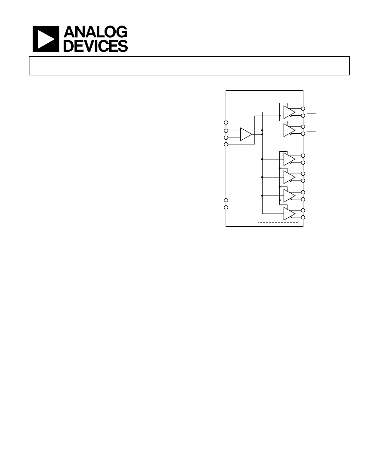
FUNCTIONAL BLOCK DIAGRAM
LVDS/CMOS
LVDS/CMOS
Figure 1.
OUT0 (OUT0A)
OUT0 (OUT0B)
OUT1 (OUT1A)
OUT1 (OUT1B)
OUT2 (OUT2A)
OUT2 (OUT2B)
OUT3 (OUT3A)
OUT3 (OUT3B)
OUT4 (OUT4A)
OUT4 (OUT4B)
OUT5 (OUT5A)
OUT5 (OUT5B)
7226-001
V
REF
CLK
CLK
CTRL_A
CTRL_B
SLEEP
ADCLK846
GENERAL DESCRIPTION
The ADCLK846 is a 1.2 GHz/250 MHz, LVDS/CMOS, fanout
buffer optimized for low jitter and low power operation. Possible
configurations range from 6 LVDS to 12 CMOS outputs,
including combinations of LVDS and CMOS outputs. Two
control lines are used to determine whether fixed blocks of
outputs are LVDS or CMOS outputs.
The clock input accepts various types of single-ended and
differential logic levels including LVPECL, LVDS, HSTL, CML,
and CMOS.
Tabl e 8 provides interface options for each type of connection.
The SLEEP pin enables a sleep mode to power down the device.
This device is available in a 24-pin LFCSP package. It is specified
for operation over the standard industrial temperature range of
−40°C to +85°C.
Rev. B
Information furnished by Analog Devices is believed to be accurate and reliable. However, no
responsibility is assumed by Analog Devices for its use, nor for any infringements of patents or other
rights of third parties that may result from its use. Specifications subject to change without notice. No
license is granted by implication or otherwise under any patent or patent rights of Analog Devices.
Trademarks and registered trademarks are the property of their respective owners.
One Technology Way, P.O. Box 9106, Norwood, MA 02062-9106, U.S.A.
Tel: 781.329.4700 www.analog.com
Fax: 781.461.3113 ©2009–2010 Analog Devices, Inc. All rights reserved.

ADCLK846
TABLE OF CONTENTS
Features .............................................................................................. 1
Applications ....................................................................................... 1
Functional Block Diagram .............................................................. 1
General Description ......................................................................... 1
Revision History ............................................................................... 2
Specifications ..................................................................................... 3
Electrical Characteristics ............................................................. 3
Timing Characteristics ................................................................ 4
Clock Characteristics ................................................................... 5
Logic and Power Characteristics ................................................ 5
Absolute Maximum Ratings ............................................................ 6
Determining Junction Temperature .......................................... 6
ESD Caution .................................................................................. 6
Thermal Performance .................................................................. 6
Pin Configuration and Function Descriptions ............................. 7
Typical Performance Characteristics ..............................................8
Functional Description .................................................................. 11
Clock Inputs ................................................................................ 11
AC-Coupled Applications ......................................................... 11
Clock Outputs ............................................................................. 12
Control and Function Pins ........................................................ 12
Power Supply ............................................................................... 12
Applications Information .............................................................. 13
Using the ADCLK846 Outputs for ADC Clock
Applications ................................................................................ 13
LVDS Clock Distribution .......................................................... 13
CMOS Clock Distribution ........................................................ 13
Input Termination Options ....................................................... 14
Outline Dimensions ....................................................................... 15
Ordering Guide .......................................................................... 15
REVISION HISTORY
5/10—Rev. A to Rev. B
Changes to Integrated Random Jitter Conditions ........................ 4
6/09—Rev. 0 to Rev. A
No Content Updates ...................................................... Throughout
4/09—Revision 0: Initial Version
Rev. B | Page 2 of 16
ADCLK846
SPECIFICATIONS
ELECTRICAL CHARACTERISTICS
Typical values are given for VS = 1.8 V and TA = 25°C, unless otherwise noted. Minimum and maximum values are given over the full
V
= 1.8 V ± 5% and TA = −40°C to +85°C variations, unless otherwise noted. Input slew rate > 1 V/ns, unless otherwise noted.
S
Table 1.
Parameter Symbol Min Typ Max Unit Conditions
CLOCK INPUTS Differential input
Input Frequency 0 1200 MHz
Input Sensitivity, Differential 150 mV p-p
Input Level 1.8 V p-p
Input Common-Mode Voltage VCM V
Input Common-Mode Range V
0.4 VS − 0.4 V
CMR
/2 − 0.1 VS/2 + 0.05 V Inputs are self-biased; enables ac coupling
S
Input Voltage Offset 30 mV
Input Sensitivity, Single-Ended 150 mV p-p
Input Resistance (Differential) 7 kΩ
Input Capacitance CIN 2 pF
Input Bias Current (Each Pin) −350 +350 µA Full input swing
LVDS CLOCK OUTPUTS
Output Frequency 1200 MHz See Figure 9 for a swing vs. frequency plot
Differential Output Voltage VOD 247 344 454 mV
∆VOD 50 mV
Offset Voltage VOS 1.125 1.25 1.375 V
∆VOS 50 mV
Short-Circuit Current ISA, ISB 3 6 mA Each pin (output shorted to GND )
CMOS CLOCK OUTPUTS
Output Frequency 250 MHz
Output Voltage High VOH V
V
− 0.1 V At 1 mA load
S
− 0.35 V At 10 mA load
S
Output Voltage Low VOL 0.1 V At 1 mA load
0.35 V At 10 mA load
Reference Voltage V
REF
Output Voltage VS/2 − 0.1 VS/2 VS/2 + 0.1 V ±500 µA
Output Resistance 60 Ω
Output Current 500 µA
Jitter performance is improved with higher slew
rates (greater voltage swing)
Larger voltage swings can turn on the protection
diodes and can degrade jitter performance
Inputs are dc-coupled with 200 mV p-p signal
applied
CLK ac-coupled; CLK
Termination = 100 Ω; differential (OUTx, OUTx
ac-bypassed to ground
)
Single-ended; termination = open
OUTx and OUTx
in phase
With 10 pF load each output; see Figure 16 for
swing vs. frequency
Rev. B | Page 3 of 16
ADCLK846
TIMING CHARACTERISTICS
Table 2.
Parameter Symbol Min Typ Max Unit Conditions
LVDS OUTPUTS Termination = 100 Ω differential; 3.5 mA
Output Rise/Fall Time tR, tF 135 235 ps 20% to 80% measured differentially
Propagation Delay, CLK-to-LVDS Output tPD 1.5 2.0 2.7 ns V
Temperature Coefficient 2.0 ps/°C
Output Skew1
All LVDS Outputs on the Same Part 65 ps
All LVDS Outputs Across Multiple Parts 390 ps
Additive Time Jitter
Integrated Random Jitter 54 fs rms BW = 12 kHz to 20 MHz, CLK = 1000 MHz
74 fs rms BW = 50 kHz to 80 MHz, CLK = 1000 MHz
86 fs rms BW = 10 Hz to 100 MHz, CLK = 1000 MHz
Broadband Random Jitter2 150 fs rms Input slew rate = 1 V/ns
Crosstalk-Induced Jitter 260 fs rms
CMOS OUTPUTS Termination = open
Output Rise/Fall Time tR, tF 525 950 ps 20% to 80%; CMOS load = 10 pF
Propagation Delay, CLK-to-CMOS Output tPD 2.5 3.2 4.2 ns 10 pF load
Temperature Coefficient 2.2 ps/°C
Output Skew2
All CMOS Outputs on the Same Part 175 ps
All CMOS Outputs Across Multiple Parts 640 ps
Additive Time Jitter
Integrated Random Jitter 56 fs rms BW = 12 kHz to 20 MHz, CLK = 200 MHz
Broadband Random Jitter3 100 fs rms Input slew = 2 V/ns; see Figure 11
Crosstalk-Induced Jitter 260 fs rms
LVDS-TO-CMOS OUTPUT SKEW2
LVDS Output(s) and CMOS Output(s)
0.8 1.6 ns CMOS load = 10 pF and LVDS load = 100 Ω
on the Same Part
1
This is the difference between any two similar delay paths while operating at the same voltage and temperature.
2
Measured at rising edge of clock signal.
3
Calculated from SNR of ADC method.
= V
ICM
, VID = 0.5 V
REF
Calculated from spur energy with an interferer
10 MHz offset from carrier
Calculated from spur energy with an interferer
10 MHz offset from carrier
Rev. B | Page 4 of 16
ADCLK846
CLOCK CHARACTERISTICS
Table 3. Clock Output Phase Noise
Parameter Min Typ Max Unit Conditions
CLK-TO-LVDS ABSOLUTE PHASE NOISE Input slew rate > 1 V/ns
1000 MHz −90 dBc/Hz At 10 Hz offset
−108 dBc/Hz At 100 Hz offset
−117 dBc/Hz At 1 kHz offset
−126 dBc/Hz At 10 kHz offset
−134 dBc/Hz At 100 kHz offset
−141 dBc/Hz At 1 MHz offset
−146 dBc/Hz At 10 MHz offset
CLK-TO-CMOS ABSOLUTE PHASE NOISE Input slew rate > 1 V/ns
200 MHz −100 dBc/Hz At 10 Hz offset
−117 dBc/Hz At 100 Hz offset
−128 dBc/Hz At 1 kHz offset
−138 dBc/Hz At 10 kHz offset
−147 dBc/Hz At 100 kHz offset
−153 dBc/Hz At 1 MHz offset
−156 dBc/Hz At 10 MHz offset
LOGIC AND POWER CHARACTERISTICS
Table 4. Control Pin Characteristics
Parameter Symbol Min Typ Max Unit Conditions
CONTROL PINS
(CTRL_A, CTRL_B, SLEEP)
1
Logic 1 Voltage VIH V
Logic 0 Voltage VIL 0.4 V
Logic 1 Current IIH 5 8 20 A
Logic 0 Current IIL −5 +5 A
Capacitance 2 pF
POWER
Supply Voltage Requirement VS 1.71 1.8 1.89 V VS = 1.8 V ± 5%
LVDS Outputs, Full Operation
LVDS at 100 MHz 55 70 mA All outputs enabled as LVDS and loaded, RL = 100 Ω
LVDS at 1200 MHz 110 130 mA All outputs enabled as LVDS and loaded, RL = 100 Ω
CMOS Outputs, Full Operation
CMOS at 100 MHz 75 95 mA
CMOS at 250 MHz 155 190 mA
Sleep 3 mA
Power Supply Rejection2
LVDS PSR
CMOS PSR
1
These pins each have a 200 kΩ internal pull-down resistor.
2
Change in T
per change in VS.
PD
− 0.4 V
S
All outputs enabled as CMOS and loaded,
CMOS load = 10 pF
All outputs enabled as CMOS and loaded,
CMOS load = 10 pF
SLEEP pin pulled high; does not include power
dissipated in external resistors
0.9 ps/mV
TPD
1.2 ps/mV
TPD
Rev. B | Page 5 of 16

ADCLK846
ABSOLUTE MAXIMUM RATINGS
Table 5.
Parameter Rating
Supply Voltage
VS to GND 2 V
Inputs
CLK and CLK
−0.3 V to +2 V
CMOS Inputs −0.3 V to +2 V
Outputs
Maximum Voltage −0.3 V to +2 V
Voltage Reference Voltage (V
) −0.3 V to +2 V
REF
Ope rating Temperature R ange
Ambient −40°C to +85°C
Junction 150°C
Storage Temperature Range −65°C to +150°C
Stresses above those listed under Absolute Maximum Ratings
may cause permanent damage to the device. This is a stress
rating only; functional operation of the device at these or any
other conditions above those indicated in the operational
section of this specification is not implied. Exposure to absolute
maximum rating conditions for extended periods may affect
device reliability.
DETERMINING JUNCTION TEMPERATURE
To determine the junction temperature on the application PCB,
use the following formula:
T
= T
J
+ (ΨJT × PD)
CASE
where:
T
is the junction temperature (°C).
J
is the case temperature (°C) measured by the customer at
T
CASE
top center of the package.
Ψ
is indicated in Tabl e 6.
JT
PD is the power dissipation.
Val u es o f θ
design considerations. θ
approximation of T
where T
Values of θ
are provided for package comparison and PCB
JA
can be used for a first-order
JA
by the equation
J
= TA + (θJA × PD)
T
J
is the ambient temperature (°C).
A
are provided for package comparison and PCB
JB
design considerations.
ESD CAUTION
THERMAL PERFORMANCE
Table 6.
Parameter Symbol Description Value1 Unit
Junction-to-Ambient Thermal Resistance
θ
JA
Still Air Per JEDEC JESD51-2
0.0 m/sec Airflow 57.0 °C/W
Moving Air
θ
JMA
1.0 m/sec Airflow 49.8 °C/W
2.5 m/sec Airflow 44.7 °C/W
Junction-to-Board Thermal Resistance
θ
JB
Moving Air Per JEDEC JESD51-8
1.0 m/sec Airflow 35.2 °C/W
Junction-to-Case Thermal Resistance
θ
JC
Moving Air Per MIL-STD 883, Method 1012.1
Die-to-Heat Sink 2.0 °C/W
Junction-to-Top-of-Package Characterization Parameter ΨJT
Still Air Per JEDEC JESD51-2
0 m/sec Airflow 1.0 °C/W
1
Results are from simulations. The PCB is a JEDEC multilayer type. Thermal performance for actual applications requires careful inspection of the conditions in the
application to determine if they are similar to those assumed in these calculations.
Per JEDEC JESD51-6
Rev. B | Page 6 of 16

ADCLK846
PIN CONFIGURATION AND FUNCTION DESCRIPTIONS
S
S
OUT1 (OUT1A)
OUT0 (OUT0B)
V
OUT0 (OUT0A)
24
PIN 1
INDICATO R
1V
REF
2CLK
3CLK
ADCLK846
4V
TOP VIEW
S
(Not to Scale)
5CTRL_A
6CTRL_B
7
SLEEP
NOTES:
1. EXPOSED P ADDLE MUST BE CO NNECTED TO GND.
Figure 2. Pin Configuration
V
OUT1 (OUT1B)
20
19
21
23
22
18 OUT2 (OUT2A)
17 OUT2 (OUT2B)
16 V
S
15 OUT3 (OUT3A)
14 OUT 3 (OUT3B)
13 V
S
9
8
11
12
10
S
V
OUT5 (OUT5B)
OUT5 (OUT5A)
OUT4 (OUT4B)
OUT4 (OUT4A)
07226-002
Table 7. Pin Function Descriptions
Pin No. Mnemonic Description
1 V
2
Reference Voltage.
REF
CLK
Clock Input (Negative).
3 CLK Clock Input (Positive).
4, 10, 13, 16, 19, 22 VS Supply Voltage.
5 CTRL_A CMOS Input Control for Output 1 to Output 0. (0: LVDS, 1: CMOS.)
6 CTRL_B CMOS Input Control for Output 5 to Output 2. (0: LVDS, 1: CMOS.)
7 SLEEP CMOS Input for Sleep Mode. (0: normal operation, 1: sleep.)
8
OUT5
(OUT5B)
Complementary Side of Differential LVDS Output 5, or CMOS Output 5 on Channel B.
9 OUT5 (OUT5A) True Side of Differential LVDS Output 5, or CMOS Output 5 on Channel A.
11
OUT4
(OUT4B)
Complementary Side of Differential LVDS Output 4, or CMOS Output 4 on Channel B.
12 OUT4 (OUT4A) True Side of Differential LVDS Output 4, or CMOS Output 4 on Channel A.
14
OUT3
(OUT3B)
Complementary Side of Differential LVDS Output 3, or CMOS Output 3 on Channel B.
15 OUT3 (OUT3A) True Side of Differential LVDS Output 3, or CMOS Output 3 on Channel A.
17
OUT2
(OUT2B)
Complementary Side of Differential LVDS Output 2, or CMOS Output 2 on Channel B.
18 OUT2 (OUT2A) True Side of Differential LVDS Output 2, or CMOS Output 2 on Channel A.
20
OUT1
(OUT1B)
Complementary Side of Differential LVDS Output 1, or CMOS Output 1 on Channel B.
21 OUT1 (OUT1A) True Side of Differential LVDS Output 1, or CMOS Output 1 on Channel A.
23
OUT0
(OUT0B)
Complementary Side of Differential LVDS Output 0, or CMOS Output 0 on Channel B.
24 OUT0 (OUT0A) True Side of Differential LVDS Output 0, or CMOS Output 0 on Channel A.
(25) EPAD Exposed Paddle. The exposed paddle must be connected to ground.
Rev. B | Page 7 of 16

ADCLK846
TYPICAL PERFORMANCE CHARACTERISTICS
VS = 1.8 V, TA = 25°C, unless otherwise noted.
2
CH2 100mV M 200p s 10.0GS/ s CH1 –36.0mV
Figure 3. LVDS Output Waveform at 1200 MHz Figure 6. LVDS Output Waveform at 200 MHz
2.3
2.2
2.1
2.0
1.9
PROPATATI ON DELAY (ns)
1.8
1.7
0.1 1.71.51.31.10.90.70.50.3
INPUT DIFFERENTIAL (V p-p)
Figure 4. LVDS Propagation Delay vs. VID Figure 7. LVDS Propagation Delay vs. VCM
2
7226-003
07226-004
CH2 100mV M 1.0ns 10.0G S/s CH1 –36.0mV
2.4
2.3
2.2
2.1
2.0
1.9
1.8
1.7
PROPAGATION DELAY (ns)
1.6
1.5
1.4
200 1600140012001000800600400
INPUT COMMON-MODE (mV)
7226-006
07226-007
55
54
53
52
51
50
49
DUTY CYCLE (%)
48
47
46
45
0 200 400 600 800 1000 1200
FREQUENCY (MHz)
Figure 5. LVDS Output Duty Cycle vs. Frequency
07226-105
Rev. B | Page 8 of 16
715
705
695
685
DIFFERENTIAL OUTPUT SWING (mV p-p)
675
1.62 1.921.821.72
POWER SUPPLY (V)
Figure 8. LVDS Output Swing vs. Power Supply Voltage
07226-014

ADCLK846
–
900
800
700
600
500
DIFFERENTIAL OUTPUT SWING (mV p-p)
400
100
200
300
400
500
600
700
800
900
1000
1100
1200
1300
INPUT FREQ UENCY (MHz)
1400
Figure 9. LVDS Differential Output Swing vs. Input Frequency
1500
1600
1700
07226-009
80
–90
–100
–110
–120
–130
–140
–150
PHASE NOISE (d Bc/Hz)
–160
–170
–180
ABSOLUTE PHASE NOISE ME ASURED @ 1GHz WI TH AGILENT
E5052 USING WENZEL CLOCK SOURCE CONSISTING OF A
WENZEL 100MHz CRYSTAL OSCILLATOR (P/N 500-06672),
WENZEL 5× MULTIPLIER (P/N LNOM-100-5-13-14-F-A), AND A
WENZEL 2× MULTIPLIER (P/N LNDD-500-14-14-1-D).
ADCLK846
CLOCK SOURCE
10 100M10M1M100k10k1k100
FREQUENCY OFFSET (Hz)
Figure 12. Absolute Phase Noise LVDS at 1000 MHz
07226-112
150
125
100
75
CURRENT (mA)
50
25
0
0 200 400 600 800 1000 1200 1400 1600 1800
FREQUENCY (MHz)
Figure 10. LVDS Current vs. Frequency, All Banks Set to LVDS
500
450
400
350
300
rms)
S
250
200
JITTER (f
150
100
50
0
022.01.51.00.5
INPUT SLEW RATE (V/ns)
Figure 11. Additive Broadband Jitter vs. Input Slew Rate
200
150
100
CURRENT (mA)
50
BANK A LVDS,
BANK B CMOS
0
25 50 75 100 125 150 175 225200 250
07226-110
FREQUENCY (MHz )
Figure 13. LVDS/CMOS Current vs. Frequency with Various Logic
Combinations
55
54
53
52
51
50
49
DUTY CYCLE (%)
48
47
46
45
.5
07226-011
0 50 100 150 200 250
FREQUENCY (MHz)
Figure 14. CMOS Output Duty Cycle vs. Frequency, 10 pF Load
BOTH BANKS CMOS
BANK A CMOS,
BANK B LVDS
BOTH BANKS LVDS
07226-113
07226-114
Rev. B | Page 9 of 16

ADCLK846
1
CH1 300mV 1.25n s/DIV CH1 954mV
7226-115
1
CH1 300mV 5. 0ns/DIV CH1 954mV
Figure 15. CMOS Output Waveform at 200 MHz, 10 pF Load Figure 18. CMOS Output Waveform at 50 MHz, 10 pF Load
1.9
1.8
1.7
1.6
1.5
1.4
OUTPUT SWING (V)
1.3
1.2
1.1
50 100 150 200 250
FREQUENCY (MHz)
25°C
85°C
07226-116
Figure 16. CMOS Output Swing vs. Frequency and Temperature, 10 pF Load
1.8
= 750Ω
R
L
1.7
1.6
OUTPUT SWING (V)
1.5
1.4
0220015010050
= 500Ω
R
L
R
L
FREQUENCY (MHz )
= 300Ω
Figure 19. CMOS Output Swing vs. Frequency and Resistive Load
2.0
1.9
1.8
1.7
1.6
1.5
1.4
OUTPUT SWING (V)
1.3
1.2
1.1
1.0
0 50 100 150 200 250
FREQUENCY (MHz )
Figure 17. CMOS Output Swing vs. Frequency and Capacitive Load
C
C
L
C
L
= 5pF
L
= 10pF
= 20pF
07226-017
7226-018
RL = 1kΩ
50
07226-015
Rev. B | Page 10 of 16

ADCLK846
V
FUNCTIONAL DESCRIPTION
The ADCLK846 clock input is distributed to all output channels.
Each channel bank is pin programmable for either LVDS or
CMOS levels. This allows the selection of multiple logic
configurations ranging from 6 LVDS to 12 CMOS outputs,
along with other combinations using both types of logic.
CLOCK INPUTS
The differential inputs of the ADCLK846 are internally selfbiased. The clock inputs have a resistor divider, which sets the
common-mode level for the inputs. The complementary inputs
are biased about 30 mV lower than the true input to avoid
oscillations if the input signal ceases. See Figure 20 for
the equivalent input circuit.
The inputs can be ac-coupled or dc-coupled. Tab l e 8 displays
a guide for input logic compatibility. If a single-ended input is
desired, this can be accommodated by ac or dc coupling to one
side of the differential input. Bypass the other input to ground
by a capacitor.
Note that jitter performance degrades with low input slew rate,
as shown in Figure 11. See Figure 28 through Figure 32 for
different termination schemes.
9kΩ 9.5kΩ
CLK
9kΩ 8.5kΩ
Figure 20. ADCLK846 Input Stage
AC-COUPLED APPLICATIONS
When ac coupling is desired, the ADCLK846 offers two
options. The first option requires no external components
(excluding the dc blocking capacitor); it allows the user to
couple the reference signal onto the clock input pins (see
Figure 31).
The second option allows the use of the V
bias level for the ADCLK846. The V
to CLK and
impedance termination of signals at the ADCLK846 (see
The internal bias resistors are still in parallel with the external
biasing. However, the relatively high impedance of the internal
resistors allows the external termination to V
This is also useful if it is not desirable to offset the inputs slightly
as previously mentioned using only the internal biasing.
CLK
through resistors. This method allows lower
). Figure 32
S
CLK
GND
07226-023
pin to set the dc
REF
pin can be connected
REF
to dominate.
REF
Table 8. Input Logic Compatibility
Supply (V) Logic Common Mode (V) Output Swing (V) AC-Coupled DC-Coupled
3.3 CML 2.9 0.8 Yes Not allowed
2.5 CML 2.1 0.8 Yes Not allowed
1.8 CML 1.4 0.8 Yes
3.3 CMOS 1.65 3.3 Not allowed
2.5 CMOS 1.25 2.5 Not allowed
1.8 CMOS 0.9 1.8 Yes
1.5 HSTL 0.75 0.75 Yes
LVDS 1.25 0.4 Yes
3.3 LVPECL 2.0 0.8 Yes
2.5 LVPECL 1.2 0.8 Yes
Yes
Not allowed
Not allowed
Yes
Yes
Yes
Not allowed
Yes
1.8 LVPECL 0.5 0.8 Yes Yes
Rev. B | Page 11 of 16

ADCLK846
A
V
A
V
V
CLOCK OUTPUTS
Each driver consists of a differential LVDS output or two singleended CMOS outputs (always in phase). When the LVDS driver
is enabled, the corresponding CMOS driver is in tristate. When
the CMOS driver is enabled, the corresponding LVDS driver is
powered down and tristated. Figure 21 and Figure 22 display
the equivalent output stage.
S
3.5m
OUTx
OUTx
3.5m
Figure 21. LVDS Output Simplified Equivalent Circuit
S
07226-024
S
POWER SUPPLY
The ADCLK846 requires a 1.8 V ± 5% power supply for VS.
Best practice recommends bypassing the power supply on
the PCB with adequate capacitance (>10 µF) and bypassing
all power pins with adequate capacitance (0.1 µF) as close to
the part as possible. The layout of the ADCLK846 evaluation
board (ADCLK846/PCBZ) provides a good layout example.
Exposed Metal Paddle
The exposed metal paddle on the ADCLK846 package is an
electrical connection, as well as a thermal enhancement. For
the device to function properly, the paddle must be properly
attached to ground (GND). The ADCLK846 dissipates heat
through its exposed paddle. The PCB acts as a heat sink for the
ADCLK846. The PCB attachment must provide a good thermal
path to a larger heat dissipation area, such as the ground plane
on the PCB. This requires a grid of vias from the top layer down
to the ground plane. See Figure 23 for an example.
OUTxA
Figure 22. CMOS Equivalent Output Circuit
OUTxB
7226-025
CONTROL AND FUNCTION PINS
Logic Select for CTRL_A
CTRL_A selects either CMOS (high) or LVDS (low) logic for
Output 1 and Output 0. This pin has an internal 200 k pulldown resistor.
Logic Select for CTRL_B
CTRL_B selects either CMOS (high) or LVDS (low) logic for
Output 5, Output 4, Output 3, and Output 2. This pin has an
internal 200 k pull-down resistor.
Sleep Mode
SLEEP powers down the chip except for the band gap. The
input is active high, which puts the outputs into a high-Z state.
This pin has a 200 k pull-down resistor. The control pins are
operational during sleep mode.
VIAS TO G ND PLANE
Figure 23. PCB Land Example for Attaching Exposed Paddle
07226-026
Rev. B | Page 12 of 16

ADCLK846
V
V
Ω
APPLICATIONS INFORMATION
USING THE ADCLK846 OUTPUTS FOR ADC CLOCK APPLICATIONS
Any high speed analog-to-digital converter (ADC) is extremely
sensitive to the quality of the sampling clock provided by the
user. An ADC can be thought of as a sampling mixer, and any
noise, distortion, or timing jitter on the clock is combined with
the desired signal at the ADC output. Clock integrity requirements scale with the analog input frequency and resolution,
with higher analog input frequency applications at ≥14-bit
resolution being the most stringent. The theoretical SNR of
an ADC is limited by the ADC resolution and the jitter on
the sampling clock. Considering an ideal ADC of infinite
resolution where the step size and quantization error can be
ignored, the available SNR can be expressed approximately by
LVDS CLOCK DISTRIBUTION
The ADCLK846 provides clock outputs that are selectable
as either CMOS or LVDS level outputs. LVDS is a differential
output option that uses a current-mode output stage. The
nominal current is 3.5 mA, which yields 350 mV output swing
across a 100 Ω resistor. The LVDS output meets or exceeds all
ANSI/TIA/EIA-644 specifications. A recommended termination circuit for the LVDS outputs is shown in Figure 25.
If ac coupling is necessary, place decoupling capacitors either
before or after the 100 Ω termination resistor.
S
LVDS
DIFFERENTIAL (COUPLED)
100Ω
100Ω
S
LVDS
=
SNR
20log
⎡
⎢
⎢
⎣
2π
⎤
1
⎥
Tf
⎥
J
A
⎦
where:
is the highest analog frequency being digitized.
f
A
is the rms jitter on the sampling clock.
T
J
Figure 24 shows the required sampling clock jitter as a function
of the analog frequency and effective number of bits (ENOB).
See AN-756 Application Note and AN-501 Application Note
for more information.
110
100
90
80
70
SNR (dB)
60
50
40
30
10 1k100
f
FULL-SCAL E SINE WAVE ANALOG FREQUENCY (MHz)
A
SNR = 20log
T
J
=
1
0
2
0
0
f
S
4
0
0
f
S
1
p
s
2
p
s
1
0
p
s
0
f
Figure 24. SNR and ENOB vs. Analog Input Frequency
2πf
S
1
ATJ
18
16
14
12
ENOB
10
8
6
Many high performance ADCs feature differential clock inputs
to simplify the task of providing the required low jitter clock on
a noisy PCB. Distributing a single-ended clock on a noisy PCB
can result in coupled noise on the sample clock. Differential
distribution has inherent common-mode rejection that can
provide superior clock performance in a noisy environment.
The ADCLK846 features LVDS outputs that provide differential
clock outputs, which enable clock solutions that maximize converter SNR performance. Consider the input requirements of
the ADC (differential or single-ended, logic level, termination)
when selecting the best clocking/converter solution.
07226-028
Figure 25. LVDS Output Termination
See the AN-586 Application Note at www.analog.com for more
information on LVDS.
CMOS CLOCK DISTRIBUTION
The output drivers of the ADCLK846 can also be configured
as CMOS drivers. When selected as a CMOS driver, each
output becomes a pair of CMOS outputs. These outputs are
1.8 V CMOS compatible.
When single-ended CMOS clocking is used, some of the
following guidelines outlined in this section apply.
Design point-to-point connections such that each driver has
only one receiver, if possible. Connecting outputs in this manner
allows for simple termination schemes and minimizes ringing
due to possible mismatched impedances on the output trace.
Series termination at the source is generally required to provide
transmission line matching and/or to reduce current transients
at the driver.
The value of the resistor is dependent on the board design and
timing requirements (typically 10 Ω to 100 Ω is used). CMOS
outputs are also limited in terms of the capacitive load or trace
length that they can drive. Typically, trace lengths less than
07226-027
3 inches are recommended to preserve signal rise/fall times
and signal integrity.
60.4
(1.0 INCH)
10Ω
CMOS CMOS
Figure 26. Series Termination of CMOS Output
MICROSTRIP
07226-076
Rev. B | Page 13 of 16

ADCLK846
V
V
Termination at the far end of the PCB trace is a second option.
The CMOS outputs of the ADCLK846 do not supply enough
current to provide a full voltage swing with a low impedance
resistive, far-end termination, as shown in Figure 27. Match the
far-end termination network to the PCB trace impedance and
provide the desired switching point. The reduced signal swing
may still meet receiver input requirements in some applications.
This can be useful when driving long trace lengths on less
critical nets.
S
10Ω
CMOS CMOS
50Ω
100Ω
100Ω
7226-077
Figure 27. CMOS Output with Far-End Termination
Because of the limitations of single-ended CMOS clocking,
consider using differential outputs when driving high speed
signals over long traces. The ADCLK846 offers LVDS outputs
that are better suited for driving long traces where the inherent
noise immunity of differential signaling provides superior
performance for clocking converters.
INPUT TERMINATION OPTIONS
For single-ended operation, always bypass unused input to
GND as shown in Figure 31.
Figure 32 illustrates the use of the V
ance termination into V
/2. In addition, Figure 32 shows a way
S
to negate the 30 mV input offset with external resistor values.
For example, use 1.8 V CMOS with long traces to provide farend termination.
CLK
100Ω
CLK
to provide low imped-
REF
CC
CLK
CLK
V
CC
CLK
CLK
7226-129
Figure 29. Typical AC-Coupled or DC-Coupled CML Configurations
(see Table 8 for CML Coupling Limitations)
CLK
CLK
50Ω 50Ω
– 2V
V
CC
CLK
CLK
50Ω 50Ω
– 2V
V
CC
07226-130
Figure 30. Typical AC-Coupled or DC-Coupled LVPECL Configurations
(see Table 8 for LVPECL DC Coupling Limitations)
CLK
CLK
CLK
CLK
CLK
100Ω
CLK
7226-128
Figure 28. Typical AC-Coupled or DC-Coupled LVDS or HSTL Configurations
(see Table 8)
Figure 31. Typical 1.8 V CMOS Configurations for Short Trace Lengths
CLK
CLK
(see Table 8 for CMOS compatibility)
07226-131
V
REF
CLK
CLK
Figure 32. Use of the V
to Provide Low Impedance Termination into VS/2
REF
07226-132
Rev. B | Page 14 of 16

ADCLK846
OUTLINE DIMENSIONS
4.00
PIN 1
INDICATOR
1.00
0.85
0.80
SEATING
PLANE
12° MAX
BSC SQ
TOP
VIEW
0.80 MAX
0.65 TYP
*
COMPLIANT TO JEDEC STANDARDS MO -220-VGGD-2
EXCEPT FOR EXPOSED PAD DIMENSION
0.30
0.23
0.18
3.75
BSC SQ
0.20 REF
0.05 MAX
0.02 NOM
COPLANARITY
0.60 MAX
0.50
BSC
0.50
0.40
0.30
0.08
Figure 33. 24-Lead Lead Frame Chip Scale Package [LFCSP_VQ]
4 mm × 4 mm Body, Very Thin Quad
CP-24-2
Dimensions shown in millimeters
0.60 MAX
PIN 1
INDICATOR
1
24
19
18
EXPOSED
PA D
(BOTTOMVIEW)
13
12
7
2.50 REF
FOR PROPER CONNE CTION OF
THE EXPOSED PAD, REFER TO
THE PIN CONF IGURATIO N AND
FUNCTION DES CRIPTIONS
SECTION O F THIS DAT A SHEET.
*
2.45
2.30 SQ
2.15
6
0.23 MIN
080808-A
ORDERING GUIDE
Model1 Temperature Range Package Description Package Option
ADCLK846BCPZ
ADCLK846BCPZ-REEL7
ADCLK846/PCBZ Evaluation Board
1
Z = RoHS Compliant Part.
−40°C to +85°C 24-Lead LFCSP_VQ CP-24-2
−40°C to +85°C 24-Lead LFCSP_VQ CP-24-2
Rev. B | Page 15 of 16

ADCLK846
NOTES
©2009–2010 Analog Devices, Inc. All rights reserved. Trademarks and
registered trademarks are the property of their respective owners.
D07226-0-5/10(B)
Rev. B | Page 16 of 16
 Loading...