

Page 1
Audio Codec with
www.BDTIC.com/ADI
FEATURES
Fully programmable audio digital signal processing (DSP) for
enhanc
ed sound processing
Scalable digital audio delay line
Pool of 400 ms @ 48 kHz (200 ms for stereo channel)
High performance, integrated analog-to-digital converters
ADCs) and digital-to-analog converters (DACs)
(
1 stereo analog input (ADC)
4 stereo analog inputs with mux-to-stereo ADC
4 stereo (8-channel) analog outputs (DACs)
Dedicated headphone output with integrated amplifier
Multichannel digital I/O
8-channel I
8- and 16-channel TDM input and output modes
2-channel (1 stereo) asynchronous I
integrated sample rate converter (SRC), supporting
sample rates from 5 kHz to 50 kHz
2
S input and output modes
2
S input with
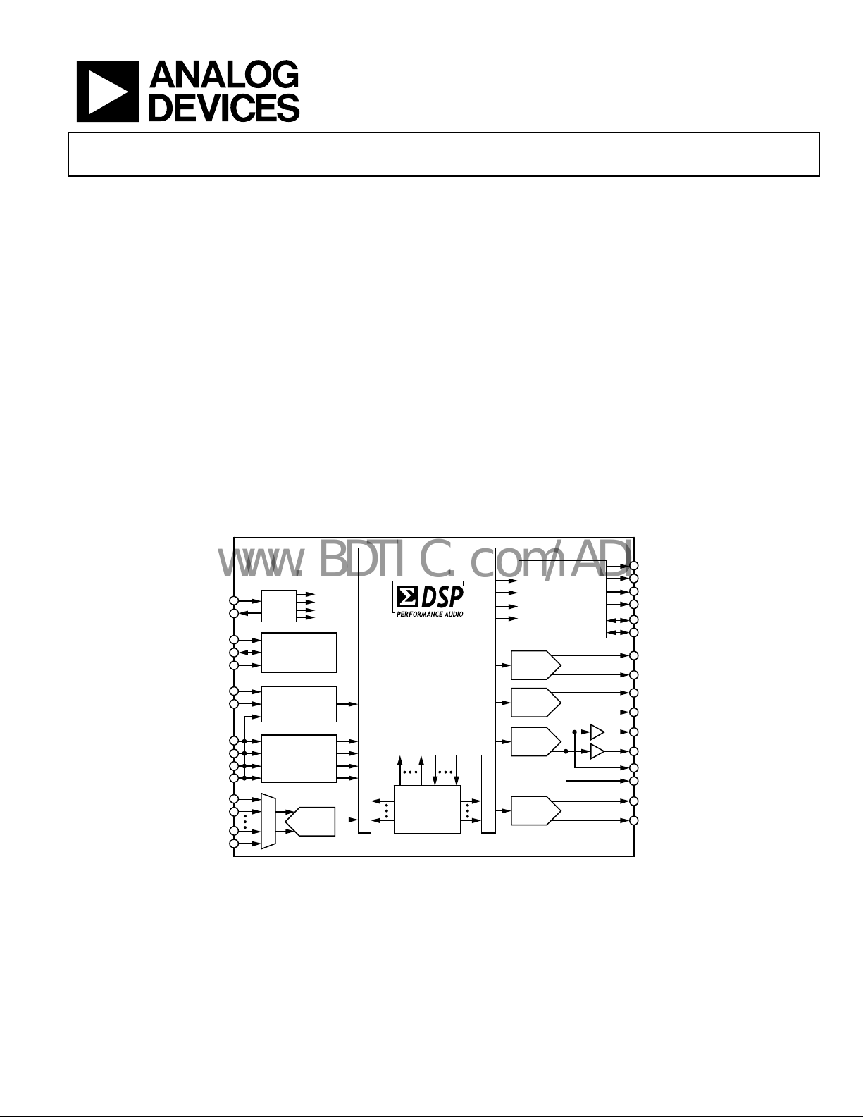
FUNCTIONAL BLOCK DIAGRAM
Embedded SigmaDSP Processor
ADAV400
Features SigmaStudio™, a proprietary graphical
programming tool for fast development of custom
signal flows
Includes various third-party audio algorithms
2
C control interface
I
Operates from 3.3 V (analog), 1.8 V (digital core),
V (digital interface)
3.3
Features on-chip regulator for single 3.3 V operation
80-lead LQFP (14 mm × 14 mm)
Temperature range: 0°C to 70°C
APPLICATIONS
ATV and AV audio applications
TV audio processing
Set-top box (STB)
HTiB
General audio enhancement
MCLKI
MCLKO
SCL
SDA
AD0
BCLK0
LRCLK0
SDIN0
SDIN1
SDIN2
SDIN3
AINL1
AINR1
AINL4
AINR4
ADAV400
PLL
2
C INTERFACE
I
SRC
ASYNCHRONIZE
DIGITAL INPU T
SYNCHRONIZE
MULTICHANNEL
DIGITAL INPUT
ADC
SYSTEM
CLOCKS
PROGRAMMABLE
AUDIO
PROCESSOR
CORE
A–V
SYNC DELAY
MEMORY
Figure 1.
MULTICHANNEL
DIGITAL OUTPUTS
DAC
DAC
DAC
DAC
SDO0
SDO1
SDO2
SDO3
LRCLK1
BCLK1
VOUT1
VOUT2
VOUT3
VOUT4
HPOUTL
HPOUTR
AUXL1
AUXR1
AUXL2
AUXR2
05811-001
Rev. A
Information furnished by Analog Devices is believed to be accurate and reliable. However, no
responsibility is assumed by Anal og Devices for its use, nor for any infringements of patents or ot her
rights of third parties that may result from its use. Specifications subject to change without notice. No
license is granted by implication or otherwise under any patent or patent rights of Analog Devices.
Trademarks and registered trademarks are the property of their respective owners.
One Technology Way, P.O. Box 9106, Norwood, MA 02062-9106, U.S.A.
Tel: 781.329.4700 www.analog.com
Fax: 781.461.3113 ©2006–2007 Analog Devices, Inc. All rights reserved.
Page 2

ADAV400
www.BDTIC.com/ADI
TABLE OF CONTENTS
Features.............................................................................................. 1
RAMs and Registers....................................................................... 19
Applications....................................................................................... 1
Functional Block Diagram .............................................................. 1
Revision History ............................................................................... 2
General Description ......................................................................... 3
Specifications..................................................................................... 4
Digital Timing............................................................................... 6
Absolute Maximum Ratings............................................................ 8
ESD Caution.................................................................................. 8
Pin Configuration and Function Descriptions............................. 9
Typical Performance Characteristics ...........................................11
Theory of Operation ...................................................................... 13
Analog Inputs.............................................................................. 13
Sample Rate Converter Block ................................................... 13
PLL Block..................................................................................... 13
Analog Outputs........................................................................... 13
Control Port Addressing ........................................................... 19
Parameter RAM Contents......................................................... 19
Recommended Program/Parameter Loading Procedures.... 20
Target/Slew RAM ....................................................................... 20
Safe Load Registers..................................................................... 23
Data Capture Registers.............................................................. 23
Control Port Read/Write Data Formats .................................. 24
Serial Data Input/Output Ports .................................................... 26
Control Registers............................................................................ 28
Audio Core Control Register .................................................... 31
RAM Modulo Control Register................................................ 32
Serial Output Control Registers ............................................... 32
Serial Input Control Register .................................................... 32
SRC Serial Port Control Register ............................................. 33
ADC Input Mux Register.......................................................... 33
Headphone Amplifier................................................................ 14
Voltage Regulator .......................................................................14
Control Port.....................................................................................15
2
I
C Port ........................................................................................ 15
Signal Processing ............................................................................ 18
Numeric Formats........................................................................ 18
Programming.............................................................................. 18
REVISION HISTORY
7/07—Rev. 0 to Rev. A
Change to ADC Section, Total Harmonic Distortion + Noise......... 4
Change to DAC Outputs (Single-Ended),
Total Harmonic Distortion + Noise.................................................. 4
Changes to Ordering Guide...................................................................35
1/06—Revision 0: Initial Version
Power Control Register ............................................................. 33
User Control Register 2 ............................................................. 33
User Control Register 1 ............................................................. 33
DAC Amplifier Register ............................................................ 33
Typical Application Diagram........................................................ 34
Outline Dimensions....................................................................... 35
Ordering Guide .......................................................................... 35
Rev. A | Page 2 of 36
Page 3

ADAV400
www.BDTIC.com/ADI
GENERAL DESCRIPTION
The ADAV400 is an enhanced audio processor. Integrating high
performance analog and digital I/Os with a powerful, audiospecific, programmable core enables designers to differentiate
their products through audio performance.
The audio processing core is based on Analog Devices SigmaDSP®
t
echnology featuring full 28-bit processing (56-bit in double
precision mode); a sophisticated, fully programmable dynamics
processor; and delay memory.
This technology allows the system designer to compensate for
re
al-world limitations of speakers, amplifiers, and listening
environments. This compensation results in a dramatic
improvement of the perceived audio quality through speaker
equalization, multiband compression and limiting, and thirdparty-branded algorithms.
The analog I/O integrates Analog Devices proprietary continuous
t
ime, multibit, sigma-delta (Σ-) architecture. This integration
brings a higher level of performance to systems that are
required to meet system branding certification by third-party
algorithm providers. The analog inputs feature a 95 dB dynamic
range stereo ADC fed from a four-stereo input mux. The four
stereo analog outputs are each driven by a 95 dB dynamic range
DAC. A dedicated headphone channel is included with
integrated amplifiers.
The ADAV400 supports multichannel digital inputs and outputs.
n integrated SRC on one channel provides the capability to
A
support any input sample rate in the range of 5 kHz to 50 kHz,
synchronizing this input to the internal DSP engine.
The ADAV400 is supported by a powerful graphical programming
t
ool that includes blocks such as general filters, EQ filters, dynamics
processing, mixers, volume, and third-party algorithms for fast
development of custom signal flows.
Rev. A | Page 3 of 36
Page 4
ADAV400
www.BDTIC.com/ADI
SPECIFICATIONS
AV DD n1 = 3.3 V, ODVDD = 3.3 V, DVDD = internal voltage regulator, temperature = 0°C to 70°C, master clock = 12.288 MHz,
measurement bandwidth = 20 Hz to 20 kHz, ADC input signal = 1 kHz, DAC output signal = 1 kHz, unless otherwise noted.
Table 1.
Parameter Min Typ Max Unit Test Conditions/Comments
REFERENCE SECTION
Absolute Voltage (V
V
Temperature Coefficient 130 ppm/°C
REF
ANALOG INPUTS (SINGLE ENDED)
Number of Channels 8 Four stereo input channels
Full-Scale Analog Input 100 A rms 2 V rms input with 20 kΩ series resistor
DC Offset ±10 mV Relative to V
ADC SECTION
Resolution 24 Bits
Dynamic Range
A-Weighted 90 95 dB −60 dB with respect to full-scale analog input
Total Harmonic Distortion + Noise −90 dB −3 dB with respect to full-scale analog input
Interchannel Gain Mismatch 0.1 dB Left and right channel gain mismatch
Crosstalk −78 dB Analog channel crosstalk (AINYm2 to AINYm2)
Gain Error −6 %
Power Supply Rejection −83 dB 1 kHz, 300 mV p-p signal at AVDDn
ADC DIGITAL DECIMATOR FILTER
CHARACTERISTICS @ 48 kHz
Pass Band 22.5 kHz
Pass-Band Ripple ±0.0002 dB
Transition Band 24 kHz
Stop Band 26.5 kHz
Stop-Band Attenuation 100 dB
Group Delay 1040 s
DAC OUTPUTS (SINGLE-ENDED) DAC amplifier register contents = 0x0010
Number of Channels 8 Four stereo output channels
Resolution 24 Bits
Full-Scale Analog Output 1 V rms
Dynamic Range
A-Weighted 90 95 dB −60 dB with respect to full-scale code input
Total Harmonic Distortion + Noise
Crosstalk −100 dB Analog channel crosstalk (VOUTm2 to VOUTm2)
Gain Error 5 %
Interchannel Gain Mismatch 0.1 dB Left and right channel gain mismatch
DC Offset 1 mV Relative to V
Power Supply Rejection −87 dB 1 kHz, 300 mV p-p signal at AVDDn
DAC DIGITAL INTERPOLATION FILTER
CHARACTERISTICS @ 48 kHz
Pass Band 21.769 kHz
Pass-Band Ripple ±0.01 dB
Transition Band 23.95 kHz
Stop Band 26.122 kHz
Stop-Band Attenuation 75 dB
Group Delay 580 s
) 1.5 V
REF
3
4
3
REF
Stereo ADC
One channel = −3 dB, other channel = 0 V
1
−93 dB −3 dB with respect to full-scale code input
One channel = −3 dB, other channels = 0 V
REF
1
Rev. A | Page 4 of 36
Page 5

ADAV400
www.BDTIC.com/ADI
Parameter Min Typ Max Unit Test Conditions/Comments
HEADPHONE OUTPUT (SINGLE ENDED)
Number of Channels 2 One stereo channel
Resolution 24 Bits
Full-Scale Analog Output 1 V rms
Dynamic Range
A-Weighted 92 dB −60 dBFS with respect to full-scale code input
Total Harmonic Distortion + Noise −84 dB −3 dBFS with respect to full-scale code input
Gain Error 4 %
Interchannel Gain Mismatch 0.5 dB
DC Offset −30 mV Relative to V
Power Supply Rejection −84 dB 1 kHz, 300 mV p-p signal at AVDDn
PLL SECTION
Master Clock Input (MCLKI) 64 × fS
3
SRC
Dynamic Range
3
512 × fS MHz
A-Weighted 115 dB −60 dBFS input (worst-case input, fS = 50 kHz)
Total Harmonic Distortion + Noise −113 dB 0 dBFS input (worst-case input, fS = 50 kHz)
Sample Rate 5 50 kHz
DIGITAL INPUT/OUTPUT
Input Voltage High (VIH) 2.0 ODVDD V
Input Voltage Low (VIL) 0.8 V
Input Leakage (IIH @ VIH = ODVDD)
Input Leakage (IIL @ VIL = 0 V) −60
Output Voltage High (VOH @ IOH = 0.4 mA) 2.4
Output Voltage Low (VOL @ IOL = −3.2 mA)
10 A
A
V
0.4 V
Input Capacitance 10 pF
SUPPLIES
Analog Supplies (AVDDn)
Digital Supplies (DVDD)
1
3.15 3.30 3.45 V
1.6 1.8 2.0 V
Interface Supply (ODVDD) 3.15 3.30 3.45 V
Supply Current, Normal Mode
Analog Current (AVDD1) 90 110 mA
Digital and Interface Current 120 135 mA
PLL Current 5 6 mA
Supply Current, Power-Down Mode
Analog Current 6 8.5 mA
Digital and Interface Current 1.5 6 mA
PLL Current 5 50 µA
1
The n refers to supply number.
2
The m refers to channel number, and the Y refers to stereo channel identifier: L for left channel or R for right channel.
3
Guaranteed by design.
4
Measured on one DAC with other DACs and ADCs off.
Measured at headphone output with 32 Ω load,
headphone am
plifier register contents = 0x0001
REF
1
MCLK = 12.288 MHz, ADCs and DACs active,
headphon
e outputs active and driving a 32 Ω load,
Power control register = 0xFFFF
RESET low, MCLK = 3.074 MHz, AINx = AGND, DAC
and headphone outputs floating
Rev. A | Page 5 of 36
Page 6
ADAV400
www.BDTIC.com/ADI
DIGITAL TIMING
Table 2.
Parameter Min Max Unit Comments
MASTER CLOCK AND RESET
f
(MCLKI Frequency) 3.024 24.576 MHz
MCLKI
t
(MCLKI High) 10 ns
MCH
t
(MCLKI Low) 10 ns
MCL
t
(RESET Low Pulse Width)
RLPW
20 ns
I2C® PORT
f
(SCL Clock Frequency) 400 kHz
SCL
t
(SCL High) 0.6 µs
SCLH
t
(SCL Low) 1.3 µs
SCLL
Start Condition
t
(Setup Time) 0.6 µs Relevant for repeated start condition
SCS
t
(Hold Time) 0.6 µs The first clock is generated after this period
SCH
tDS (Data Setup Time) 100 ns
t
(SCL Rise Time) 300 ns
SCR
t
(SCL Fall Time) 300 ns
SCF
t
(SDA Rise Time) 300 ns
SDR
t
(SDA Fall Time) 300 ns
SDF
Stop Condition
t
(Setup Time) 0.6
SCSH
SERIAL PORTS
Slave Mode
t
(BCLKx High) 40
SBH
t
(BCLKx Low) 40
SBL
f
(BCLKx Frequency) 64 × fS
SBF
t
(LRCLKx Setup) 10
SLS
t
(LRCLKx Hold) 10
SLH
t
(SDINx Setup) 10
SDS
t
(SDINx Hold) 10
SDH
t
(SDOx Delay) 40 ns From BCLK falling edge
SDD
Master Mode
t
(LRCLKx Delay) 5 ns From BCLK falling edge
MLD
t
(SDOx Delay) 40 ns From BCLK falling edge
MDD
t
(SDINx Setup) 10
MDS
t
(SDINx Hold) 10
MDH
µs
ns
ns
ns To BCLK rising edge
ns From BCLK rising edge
ns To BCLK rising edge
ns From BCLK rising edge
ns From BCLK rising edge
ns From BCLK rising edge
Rev. A | Page 6 of 36
Page 7
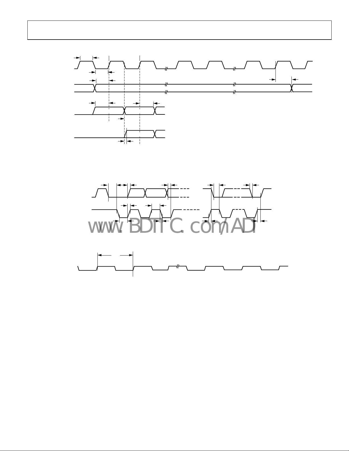
ADAV400
S
www.BDTIC.com/ADI
Digital Timing Diagrams
t
SBH
BCLKx
t
SBL
t
SLH
LRCLKx
t
SLH
SDINx
LEFT-JUSTIFIED
MODE
SDOx
I
MODE
t
SDS
MSB
2
S
t
MDD
t
SDD
MSB – 1
MSB
t
SDH
05811-002
Figure 2. Serial Port Timing
DA
SCL
t
t
SCH
SDR
t
SCR
t
SCLL
t
MP
t
SCLH
t
Figure 3. I
SCF
t
DS
2
C Port Timing
t
SCH
t
SCS
t
SDF
t
SCSH
05811-003
MCLK
05811-004
Figure 4. Master Clock T
iming
Rev. A | Page 7 of 36
Page 8

ADAV400
www.BDTIC.com/ADI
ABSOLUTE MAXIMUM RATINGS
Table 3.
Parameter Rating
DVDD to DGND 0 V to 2.2 V
ODVDD to DGND 0 V to 4.0 V
AVDD to AGND 0 V to 4.0 V
AGND to DGND −0.3 V to +0.3 V
Digital Inputs DGND − 0.3 V to ODVDD + 0.3 V
Analog Inputs AGND − 0.3 V to ADVDD + 0.3 V
Reference Voltage Indefinite short circuit to ground
Soldering (10 sec) 300°C
Stresses above those listed under Absolute Maximum Ratings
may cause permanent damage to the device. This is a stress
rating only; functional operation of the device at these or any
other conditions above those indicated in the operational
section of this specification is not implied. Exposure to absolute
maximum rating conditions for extended periods may affect
device reliability.
ESD CAUTION
Rev. A | Page 8 of 36
Page 9

ADAV400
www.BDTIC.com/ADI
PIN CONFIGURATION AND FUNCTION DESCRIPTIONS
IDAC79AINR478AINL477AINR376AINL375AINR274AINL273AINR172AINL171AVDD570AGND69AGND68AVDD467FILTD66NC65NC64TEST263AUXR262AUXL261VOUT4
80
1
FILTA
2
VREF
3
AGND
4
AVDD1
5
NC
6
NC
7
NC
8
NC
9
NC
10
NC
11
NC
12
NC
13
DGND
14
DVDD
15
AD0
16
SDA
17
SCL
18
TEST0
19
TEST1
20
DGND
NC = NO CONNECT
PIN 1
21
22
DVDD
SDIN023SDIN124SDIN225SDIN3
26
27
LRCLK0
ADAV400
(Not to Scale)
28
29
DGND
BCLK0
TOP VIEW
30
31
ODVDD
VDRIVE
DVDD
32
33
34
35
36
37
DGND
MCLKI
MCLKO
SDO038SDO1
BCLK1
LRCLK1
39NC40
DVDD
60
59
58
57
56
55
54
53
52
51
50
49
48
47
46
45
44
43
42
41
VOUT3
VOUT2
VOUT1
AUXR1
AUXL1
AVDD3
HPOUTR
HPOUTL
AGND
AGND
PLL_LF
AVDD2
DGND
DVDD
RESET
NC
NC
SDO3
SDO2
DGND
05811-005
Figure 5. Pin Configuration
Table 4. Pin Function Descriptions
Pin No. Mnemonic I/O Description
1 FILTA O ADC Filter Decoupling Node for the ADC. Decouple this pin to AGND (Pin 3).
2 VREF Voltage Reference. This pin is driven by an internal 1.5 V reference voltage. Decouple this pin to AGND (Pin 3).
3 AGND
4 AVDD1
5 to 12,
NC
ADC Ground. Connect this pin to the analog ground plane.
Analog Power Supply Pin for the ADC. Connect this pin to 3.3 V and decouple to AGND (Pin 3).
Not Connected Internally.
65, 66
13, 20,
DGND
Digital Ground. Connect this pin to the digital ground plane.
28, 32,
41, 48
14, 21,
31, 40,
DVDD
Digital Power Supply Pins. Connect these pins to 1.8 V, either directly or by using the on-chip regulator.
Decouple to DGND.
47
15 AD0 I
2
C Address Select. Tie to ODVDD for Address 0x28 (write) and Address 0x29 (read) or to DGND for
I
Address 0x2A (write) and Address 0x2B (read).
16 SDA I/O
17 SCL I
18 TEST0
19 TEST1
22 to 25 SDIN [0:3] I
26 LRCLK0 I
27 BCLK0 I
Serial Data Input/Output for the I2C Control Port.
Serial Clock for the I2C Control Port.
Test Pin. Connect to ODVDD.
Test Pin. Connect to ODVDD.
Serial Data Inputs. BCLK1 and LRCLK1 are used as the timing signals for SDIN0 to SDIN3.
Left/Right Clock for Sample Rate Converter (SRC). This input frame synchronization signal is associated
with SDIN0 to SDIN3 when one of these input channels is redirected to the SRC.
Bit Clock for Sample Rate Converter (SRC). This input clock is associated with SDIN0 to SDIN3 when one of
these input channels is redirected to the SRC.
29 ODVDD Digital Interface Supply (3.3 V) Pin. Connect this pin to a 3.3 V digital supply. Decouple to DGND.
30 VDRIVE Drive for External PNP Transistor. This is used with the on-chip 1.8 V regulator circuit.
Rev. A | Page 9 of 36
Page 10
ADAV400
www.BDTIC.com/ADI
Pin No. Mnemonic I/O Description
33 MCLKI I
34 MCLKO O Audio Clock Output. The MCLKO pin can be programmed to output the internal audio clock.
35 BCLK1 I/O
36 LRCLK1 I/O
37, 38,
42, 43
39, 44,
45
46
49 AVDD2 Analog Power Supply Pin for the PLL. Connect this pin to 3.3 V and decouple to AGND (Pin 51).
50 PLL_LF
51 AGND PLL Ground. Connect this pin to the analog ground plane.
52 AGND Headphone Driver Ground. Connect this pin to the analog ground plane.
53 HPOUTL O Left Headphone Output. Analog output from the headphone amplifiers.
54 HPOUTR O Right Headphone Output. Analog output from the headphone amplifiers.
55 AVDD3 Analog Power Supply Pin for the Headphone Amplifier. Connect this pin to 3.3 V and decouple to AGND (Pin 52).
56 AUXL1 O Auxiliary Analog Output Left 1.
57 AUXR1 O Auxiliary Analog Output Right 1.
58 to 61 VOUT [1:4] O Main Analog Output 1 to Output 4.
62 AUXL2 O Auxiliary Analog Output Left 2.
63 AUXR2 O Auxiliary Analog Output Right 2.
64 TEST2 Test Pin. This pin should be left unconnected.
67 FILTD DAC Filter Decoupling Node. Decouple this pin to AGND (Pin 69).
68 AVDD4 Analog Power Supply Pin for the DAC. Connect this pin to 3.3 V and decouple to AGND (Pin 69).
69, 70 AGND DAC Ground. Connect this pin to the analog ground plane.
71 AVDD5 Analog Power Supply Pin for the DAC. Connect this pin to 3.3 V and decouple to AGND (Pin 70).
72, 74,
76, 78
73, 75,
77, 79
80 IDAC
SDO [0:3] 0 Serial Data Outputs.
NC These pins should be left unconnected.
RESET
AINL [1:4] I
AINR [1:4] I
Master Clock Input. The ADAV400 uses a phase-locked loop (PLL) to generate the appropriate internal
or the DSP core.
clock f
Bit Clock for Serial Data Input/Output.
for the SDINx and SDOx pins. These clocks are inputs to the ADAV400 when the port is configured as a
slave, and outputs when the port is configured as a master. On power up, these pins are set to slave mode
to avoid conflicts with external master mode devices.
Left/Right Clock for Serial Data Input/
signals for the SDINx and SDOx pins.
I
Active Low Reset Signal. After RESET
PLL Loop Filter. External components are required to allow the PLL to function correctly. See the PLL
k section for details of these components.
Bloc
Left Analog Input 1 to Input 4. The analog inputs are current inputs typically driven via a 20 kΩ resistor for
2 V rms input, as shown in Figure 17.
Right Analog Input 1 to Input 4. The analog inputs are cur
for 2 V rms input, as shown in Figure 17.
DAC External Bias Resistor. This is an external bias pin f
between this pin and AGND.
This clock and the LRCLK1 are used as clock and frame sync signals
Output. This clock and the BCLK1 are used as clock and frame sync
the ADAV400 is powered down.
rent inputs typically driven via a 20 kΩ resistor
or the DAC circuitry. Connect a 20 kΩ resistor
Rev. A | Page 10 of 36
Page 11
ADAV400
www.BDTIC.com/ADI
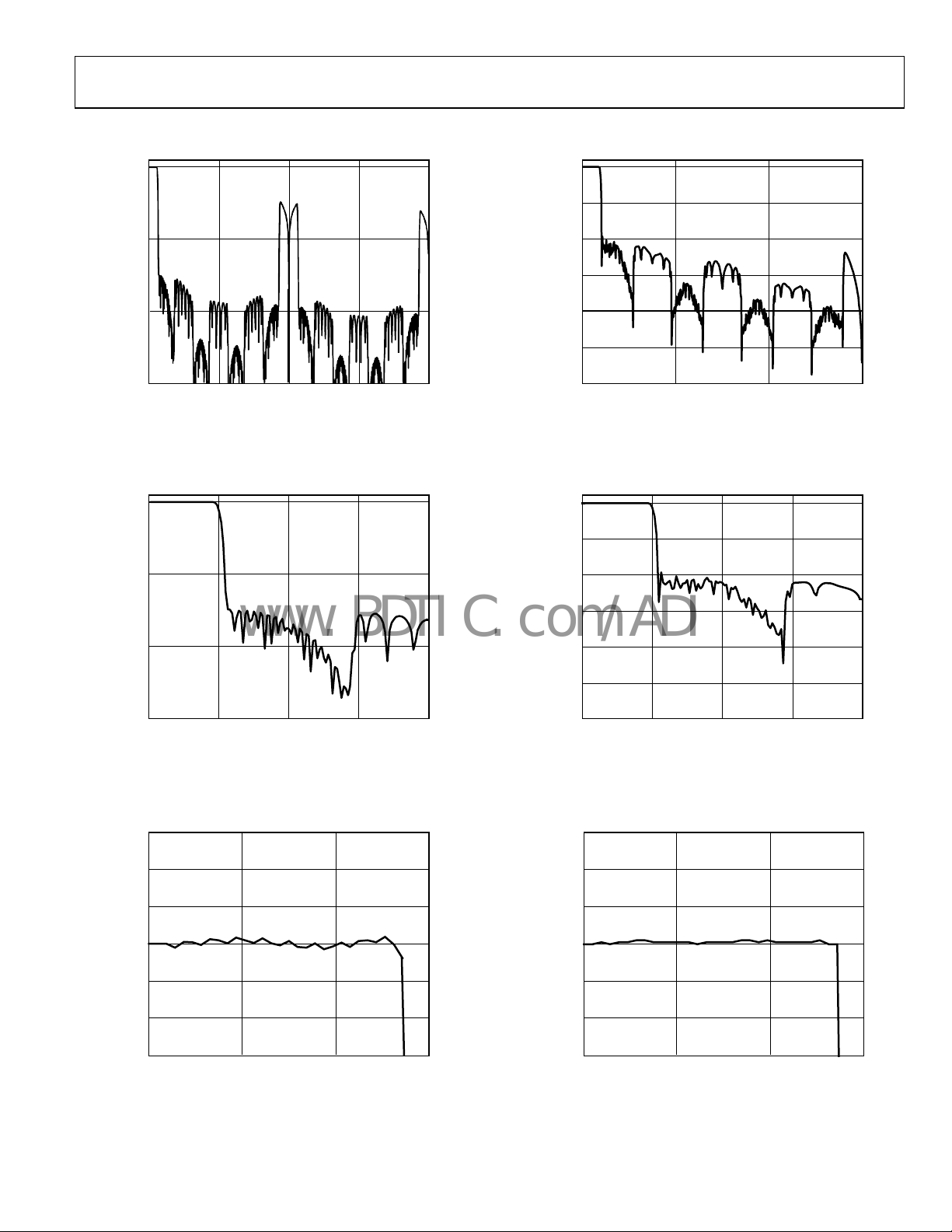
TYPICAL PERFORMANCE CHARACTERISTICS
0
0
–50
–50
MAGNITUDE (d B)
–100
–150
0 192 384 576 768
FREQUENC Y (kHz)
05811-006
–100
–150
MAGNITUDE (d B)
–200
–250
–300
0 128 256 384
FREQUENC Y (kHz)
Figure 6. DAC Composite Filter Response (48 kHz) Figure 9. ADC Composite Filter Response (48 kHz)
0
–50
MAGNITUDE (d B)
–100
0
–50
–100
–150
MAGNITUDE (d B)
–200
–250
05811-009
–150
0 2448729
FREQUENC Y (kHz)
05811-007
6
–300
0244872
FREQUENC Y (kHz)
Figure 7. DAC Pass-Band Filter Response (48 kHz) Figure 10. ADC Pass-Band Filter Response (48 kHz)
0.06
0.04
0.02
0
MAGNITUDE (d B)
–0.02
–0.04
–0.06
0 8 16 24
FREQUENC Y (kHz)
05811-008
0.006
0.004
0.002
0
MAGNITUDE (d B)
–0.002
–0.004
–0.006
0 8 16 24
FREQUENCY (kHz )
Figure 8. DAC Pass-Band Ripple (48 kHz) Figure 11. ADC Pass-Band Ripp
le (48 kHz)
05811-010
96
05811-011
Rev. A | Page 11 of 36
Page 12

ADAV400
www.BDTIC.com/ADI
–20
–40
0
DNR = 95dB
(A-WEIGHTED)
–20
–40
0
THD + N = –93dB
V
= –3dBFS
IN
–60
–80
–100
MAGNITUDE (dB)
–120
–140
–160
0 1200080004000 16000 20000
FREQUENCY (Hz)
Figure 12. DAC Dynamic Range Figure 15. ADC Total Harmonic Distortion + Noise
0
–20
–40
–60
–80
–100
MAGNITUDE (dB)
–120
THD + N = –94dB
V
= –3dBFS
IN
–60
–80
–100
MAGNITUDE (dB)
–120
–140
05811-012
–160
0 1200080004000 16000 20000
0
–5
–10
MAGNITUDE (dB)
–15
FREQUENCY (Hz)
05811-015
–140
–160
0 1200080004000 16000 20000
FREQUENCY (Hz)
Figure 13. DAC Total Harmonic Distortion + Noise
0
–20
–40
–60
–80
–100
MAGNITUDE (dB)
–120
–140
–160
0 1200080004000 16000 20000
FREQUENCY (Hz)
DNR = 95dB
(A-WEIGHTED)
05811-013
–20
0 0.1 0.2 0.3 0.4 0.5
Figure 16. Sample Rate Conv
fS (Normalized)
erter Transfer Function
05811-014
05811-037
Figure 14. ADC Dynamic Range
Rev. A | Page 12 of 36
Page 13

ADAV400
A
V
F
www.BDTIC.com/ADI
THEORY OF OPERATION
The ADAV400 is an enhanced audio processor containing an
Analog Devices SigmaDSP digital processing core. The core can
accept up to four digital stereo channels, typically at 48 kHz, or
three channels, typically at 48 kHz, and one channel at any
sample rate between 5 kHz and 50 kHz. In addition, up to four
stereo analog inputs can be used as the source for the DSP core
using the stereo ADC and a four-stereo input mux.
Outputs from the DSP core are available as four stereo digital
outputs and four stereo analog outputs.
The core of the ADAV400 is a 28-bit DSP (56-bit with double
p
recision) optimized for audio processing. Signal processing
parameters are stored in a 1024-location parameter RAM. The
program RAM can be loaded with a custom program after
power-up. New values are written to the program and parameter
RAM using the I
2
C control port. The values stored in the
parameter RAM control individual signal processing blocks,
such as IIR equalization filters, dynamics processors, audio
delays, and mixer levels. A safe load feature allows transparent
updating of these parameters, eliminating the risk of unwanted
pops or clicks in the outputs.
The ADAV400 has a sophisticated control port that supports
mplete read/write capability of all memory locations except
co
the target/slew RAM and data RAM, which are only accessible
by the DSP core.
The ADAV400 has a very flexible serial data input and output
ort that allows for glueless interconnection to a variety of
p
ADCs, DACs, general-purpose DSPs, S/PDIF receivers, and
sample rate converters. The digital inputs and outputs of the
ADAV400 can be configured in I
2
S, left-justified, right-justified,
or TDM serial port–compatible mode. They can support 16, 20,
or 24 bits in all modes. The ADAV400 accepts serial audio data
in MSB-first and twos complement formats.
The digital core of the ADAV400 operates at 1.8 V, and the other
circuit blocks operate from a 3.3 V power supply. An on-board
regulator allows a single 3.3 V supply for both digital supplies
using the configuration shown in
Figure 19.
The ADAV400 is fabricated on a single monolithic integrated
cuit and is housed in an 80-lead LQFP for operation over the
cir
0°C to 70°C consumer temperature range.
ANALOG INPUTS
The ADAV400 has four stereo analog inputs. An input
multiplexer is included that enables any of these four stereo
analog inputs to be connected to the ADC. The analog inputs
are current inputs; see
nfiguration when the required input level is 2 V rms.
co
Figure 17 for the suggested input
SAMPLE RATE CONVERTER BLOCK
The ADAV400 contains a stereo SRC that accepts input sample
rates in the range of 5 kHz to 50 kHz. Any one of the digital
inputs can be selected as the source for the SRC.
Note that the SRC has a filter cutoff frequency of 20 kHz for a
48 kHz s
ample rate. If a different input sample rate is used, the
cutoff frequency scales accordingly.
PLL BLOCK
The ADAV400 contains a phase-locked loop (PLL) that
generates all of the internal clocks required by the ADAV400.
The master clock frequency can be 64 × f
512 × f
.
S
The PLL requires some external components to operate correctly,
own in Figure 18. These components form a loop filter that
as sh
tegrates pulses from a charge pump and produces a voltage to
in
tune the VCO. Internally, the PLL can generate clocks of up
to 200 MHz, so it is recommended that a suitable capacitor be
selected.
A 3.3 V analog supply connected to AVDD2 is required to
perate the PLL. Where the supply for AVDD1 is also used for
o
the PLL, additional filtering is recommended to prevent digital
noise created by the PLL block being coupled to the analog
circuitry powered by the AVDD1 supply.
ANALOG OUTPUTS
The ADAV400 contains four stereo analog outputs typically at
1 V rms. One stereo pair of DACs is connected to integrated
headphone amplifiers HPOUTL and HPOUTR, but is also
available on the AUXL1 and AUXR1 pins.
Note that the outputs of all the DACs are inverted with the
excep
tion of the headphone channel. If required, this can be
changed using the invert library block of the DSP.
47µF
20kΩ
AINLx
47µF
20kΩ
AINRx
20kΩ
IDAC
Figure 17. Analog Input Configuration
, 128 × fS, 256 × fS, or
S
DD2
100nF
1n
Figure 18. PLL Loop Filter Components
2kΩ
BLOCK
PLL_LF
PLL
05811-016
05811-018
Rev. A | Page 13 of 36
Page 14

ADAV400
V
www.BDTIC.com/ADI
HEADPHONE AMPLIFIER
The ADAV400 has an integrated stereo headphone amplifier
capable of driving 32 mW into a 32 Ω load.
VOLTAGE REGULATOR
The ADAV400 includes an on-chip voltage regulator that
enables the chip to be used in systems where a 1.8 V supply is
not available. The only external components needed are a PNP
transistor (such as FZT953), a single capacitor, and a single
resistor. The recommended design for the voltage regulator is
shown in
As shown in this figure, VDD is the main system voltage (3.3 V).
A
connected to the DVDD pins. VDRIVE is an output from the
internal regulator circuit on the ADAV400 and is connected to
the base of the PNP transistor.
Figure 19.
voltage of 1.8 V is generated at the transistor’s collector and is
DD
+
+
ODVDD
VDRIVE
ADAV400
Figure 19. Voltage Regulator Design
DVDD
+
DVDD
There are two specifications to take into consideration when
choosing the regulator’s transistor. First, h
Second, the collector power dissipation, P
= (3.3 V − 1.8 V) × 135 mA = 202.5 mW
P
C
should be at least 100.
FE
, must be greater than
C
05811-019
Rev. A | Page 14 of 36
Page 15

ADAV400
www.BDTIC.com/ADI
CONTROL PORT
The ADAV400 control port has full read and write capability to
all registers and RAMs with the exception of the data RAM,
which is only accessible by the DSP core. Single or burst mode
reads and writes are supported. A typical word consists of the
chip address, the register or RAM subaddress, and the data to
be written. The number of bytes per data-word depends on the
address of the location being written to or read from.
The first byte of a control word (Byte 0) contains the 7-bit chip
W
ess plus the R/
addr
together form the subaddress of the memory or register location
within the ADAV400. All subsequent bytes contain data that
can be writes to the control register or updates to the program
and parameter memories.
etails on the I
d
The ADAV400 has several mechanisms for updating signal
rocessing parameters in real time without causing pops or
p
clicks. In cases where large blocks of data need to be transferred,
it is recommended to mute the output of the DSP core by setting
Bit 9 of the audio core control register to 0, and then load the
new data and set Bit 9 back to 1. This is typically done during
the booting sequence at startup or when loading a new program
into RAM.
In cases where only a few parameters need to be changed—for
exa
mple, updating a biquad—the new parameters can be loaded
without halting the program. To avoid unwanted pops or clicks
in the output during the loading sequence, the DSP core uses an
internal safe load mechanism that buffers the data and only
updates the parameter memory at the end of the sample period
and before the start of the next sample period.
bit. The next two bytes (Byte 1 and Byte 2)
2
C write and read formats.
Tabl e 16 to Ta b le 2 5 provide more
I2C PORT
The ADAV400 supports a 2-wire serial (I2C-compatible)
microprocessor bus driving multiple peripherals. Two pins,
serial data (SDA) and serial clock (SCL), carry information
between the ADAV400 and the system I
The ADAV400 is always a slave on the I
that it never initiates a data transfer. Each slave device is
recognized by a unique address.
The ADAV400 has four possible slave addresses, two for writing
o
perations and two for reading operations. These are unique
addresses for the device and are illustrated in Ta b le 5 . The LSB
o
f the byte sets either a read or a write operation; Logic Level 1
corresponds to a read operation, and Logic Level 0 corresponds
to a write operation. The seventh bit of the address is set by tying
the AD0 pin of the ADAV400 to Logic Level 0 or Logic Level 1.
2
C master controller.
2
C bus, which means
Rev. A | Page 15 of 36
Table 5. I
AD0 R/
0 0 0x28
0 1 0x29
1 0 0x2A
1 1 0x2B
Addressing
Initially, all devices on the I2C bus are in an idle state, wherein
the devices monitor the SDA and SCL lines for a start condition
and the proper address. The I
by establishing a start condition, defined by a high-to-low
transition on SDA while SCL remains high. This indicates that
an address/data stream follows. All devices on the bus respond
to the start condition and read the next byte (7-bit address +
R/
address responds by pulling the data line low during the ninth
clock pulse. This ninth bit is known as an acknowledge bit. All
other devices on the bus revert to an idle condition. The R/
bit determines the direction of the data. A Logic Level 0 on the
LSB of the first byte means the master writes information to the
peripheral. A Logic Level 1 on the LSB of the first byte means
the master reads information from the peripheral. A data
transfer takes place until a stop condition is encountered. A stop
condition occurs when SDA transitions from low to high while
SCL is held high.
Burst mode addressing, where the subaddresses are automatically
in
amounts of data to contiguous memory locations. This
increment happens automatically if a stop condition is not
encountered after a single word write. A data transfer is always
terminated by a stop condition.
Stop and start conditions can be detected at any stage during
th
sequence with normal read and write operations, it causes an
immediate jump to the idle condition. During a given SCL high
period, the user should only issue one start condition, one stop
condition, or a single stop condition followed by a single start
condition. If an invalid subaddress is issued by the user, the
ADAV400 does not issue an acknowledge and reverts to an idle
state. If the user exceeds the highest subaddress while in autoincrement mode, one of two actions is taken. In read mode, the
ADAV400 outputs the highest subaddress register contents until
the master device issues a no acknowledge, indicating the end of
a read. A no acknowledge condition is where the SDA line is not
pulled low on the ninth clock pulse on SCL. If the highest
subaddress location is reached while in write mode, the data for
the invalid byte is not loaded into any subaddress register, a no
acknowledge is issued by the ADAV400, and the part returns to
the idle condition.
2
C Addresses
W
W
bit) MSB first. The device that recognizes the transmitted
Figure 20 shows the timing of an I2C write.
cremented at word boundaries, can be used for writing large
e data transfer. If these conditions are asserted out of
Slave Address
2
C master initiates a data transfer
W
Page 16

ADAV400
www.BDTIC.com/ADI
I2C Read and Write Operations
Tabl e 6 shows the timing of a single word write operation. Every
ninth clock, the ADAV400 issues an acknowledge by pulling
SDA low.
followed by the chip address byte with the R/
The ADAV400 responds with the read result on SDA. The
master then responds every ninth clock with an acknowledge
pulse to the ADAV400.
W
set to 1 (read).
Tabl e 7 shows the timing of a burst mode write sequence. This
able shows an example where the target destination registers
t
are two bytes. The ADAV400 auto-increments its subaddress
register counter every two bytes until a stop condition occurs.
The timing of a single word read operation is shown in Tab l e 8 .
N
ote that the first R/
W
bit is still a 0, indicating a write operation.
This is because the subaddress must be written to set up the
internal address. After the ADAV400 acknowledges the receipt
of the subaddress, the master must issue a repeated start command
Key f o r Tab l e 6 t o Tabl e 9
S = start bit
top bit
P = s
AM = acknowledge by master
AS = acknowledge by slave
2
Table 6. Single Word I
S Chip address,
W
R/
= 0
C Write
AS Subaddress high AS Subaddress low AS Data Byte 1 AS Data Byte 2 … AS Data Byte N P
Tabl e 9 shows the timing of a burst mode read sequence. This
t
able shows an example where the target read registers are two
bytes. The ADAV400 increments its subaddress register every two
bytes because the requested subaddress corresponds to a
register or memory area with word lengths of two bytes. Other
address ranges may have a variety of word lengths ranging from
one to six bytes; the ADAV400 always decodes the subaddress
and sets the auto-increment circuit so that the address
increments after the appropriate number of bytes.
Table 7. Burst Mode I
S Chip
address,
W
R/
AS Subaddress
high
= 0
Table 8. Single Word I
S Chip address,
W
= 0
R/
AS Subaddress
Table 9. Burst Mode I
S Chip address,
W
R/
= 0
AS Subaddress
2
C Write
2
C Read
high
2
C Read
high
AS Subaddress
low
AS Subaddress
low
AS Subaddress
low
AS Data-Word 1,
Byte 1
AS S Chip address,
R/W = 1
AS S Chip address,
R/W = 1
AS Data-Word 1,
Byte 2
AS Data Byte 1 AM Data
AS Data-Word 1
AS Data-Word 2,
Byte 1
AM Data-Word 1
Byte 1
AS Data-Word 2,
Byte 2
… AM Data
Byte 2
Byte 2
AS … P
P
Byte N
AM … P
Rev. A | Page 16 of 36
Page 17

ADAV400
www.BDTIC.com/ADI
SCL
SDA 0
START BY
MASTER
SCL
(CONTINUED)
SDA
(CONTINUED)
SCL
SDA
START BY
MASTER
SCL
(CONTINUED)
SDA
(CONTINUED)
00
0
FRAME 1
FRAME 2
0
1
1
1
CHIP ADDRESS BYTE
SUBADDRESS BYTE 2
1
FRAME 1
CHIP ADDRESS BYTE
FRAME 3
SUBADDRESS BYTE 2
ADR
0
0
ADR
SEL
SEL
R/W0
ACK BY
ADAV400
ACK BY
ADAV400
Figure 20. I
R/W
ACK BY
ADAV400
ACK BY
ADAV400
2
C Write Format
REPEATED
START BY
MASTER
FRAME 2
SUBADDRESS BYTE 1
FRAME 3
DATA BYTE 1
FRAME 2
SUBADDRESS BYTE 1
00
1
CHIP ADDRESS BYTE
0
FRAME 4
ACK BY
ADAV400
ACK BY
ADAV400
ACK BY
ADAV400
1
ADR
0
SEL
STOP BY
MASTER
R/W
ACK BY
ADAV400
05811-021
SCL
(CONTINUED)
SDA
(CONTINUED)
FRAME 5
READ DATA BYTE 1
ACK BY
MASTER
Figure 21. I
2
C Read Format
Rev. A | Page 17 of 36
FRAME 6
READ DATA BYTE 1
ACK BY
MASTER
STOP BY
MASTER
05811-022
Page 18

ADAV400
www.BDTIC.com/ADI
SIGNAL PROCESSING
The ADAV400 is designed to provide all the signal processing
functions commonly used in stereo or multichannel playback
systems. The signal processing flow is created using a graphical
development tool supplied by Analog Devices, which allows fast
development of even complex audio flows and real-time control
of all signal processing functions.
The input and output word lengths are 24 bits. Four extra headroom bits are used in the processor to allow internal gains of up
to 24 dB without clipping.
The signal processing blocks can be arranged in a custom program
that is loaded to the RAM of the ADAV400. The available signal
processing blocks are outlined in the
Numeric Formats and
Programming sections.
NUMERIC FORMATS
It is common in DSP systems to use a standardized method of
specifying numeric formats. Fractional number systems are
specified by an A.B format, where A is the number of bits to the
left of the decimal point and B is the number of bits to the right
of the decimal point.
The ADAV400 uses the same numeric format for both the
co
efficient values (stored in the parameter RAM) and the signal
data values.
Numeric Format: 5.23
Range
−16.0 to (+16.0 − 1 LSB)
Examples
1000 0000 0000 0000 0000 0000 0000 = −16.0
1110 0000 0000 0000 0000 0000 0000 = −4.0
1111 1000 0000 0000 0000 0000 0000 = −1.0
1111 1110 0000 0000 0000 0000 0000 = −0.25
1111 1111 1111 1111 1111 1111 1111 = (1 LS
0000 0000 0000 0000 0000 0000 0000 = 0.0
0000 0010 0000 0000 0000 0000 0000 = +0.25
0000 1000 0000 0000 0000 0000 0000 = +1.0
0010 0000 0000 0000 0000 0000 0000 = +4.0
0111 1111 1111 1111 1111 1111 1111 = (+16.0 − 1 LSB)
B below 0.0)
A digital clipper circuit is used between the output of the DSP
c
ore and the serial output ports (see Figure 22). This clips the
op four bits of the signal to produce a 24-bit output with a
t
range of +1.0 (−1 LSB) to −1.0.
4-BIT SIGN EXTENSION
DATA IN SERIAL PORT
Figure 22. Numeric Precision and Clipping Structure
1.23 5.23
SIGNAL PROCESSING
(5.23 FORMAT)
DIGITAL
CLIPPER
5.23 1.23
PROGRAMMING
On power-up, the default program of the ADAV400 passes the
processed input signals to the outputs, but the outputs are
un
muted by default. There are 2560 instruction cycles per audio
sample. This DSP runs in a stream-oriented manner, meaning
all 2560 instructions are executed each sample period. The
ADAV400 can also be set up to accept double- or quad-speed
inputs by reducing the number of instructions per sample. This
is set in the audio core control register.
The part is easily programmed using graphical tools provided
b
y Analog Devices. No knowledge of DSP assembly code is
required to program the ADAV400. Simply connect graphical
blocks, such as biquad filters, dynamics processors, mixers, and
delays, in a signal flow schematic. The schematic is then
compiled, and the program and parameter files are loaded into
the program RAM of the ADAV400 through the control port.
Signal processing blocks available in the provided libraries include
• Single- and double-precision biquad filters
• Monochannel and multichannel dynamics processors
• Mixers and splitters
• Tone and noise generators
• First-order filters
• Fixed and variable gain
• RMS look-up tables
• Loudness
• Delay
• Stereo enhancement (Phat Stereo™)
• Dynamic bass boost
• Interpolators and decimators
05811-020
The serial port accepts up to 24 bits on the input and is sign-
ended to the full 28 bits of the core. This allows internal
ext
gains of up to 24 dB without encountering internal clipping.
Rev. A | Page 18 of 36
Additional blocks are always in development. Analog Devices
lso provides proprietary and third-party algorithms for appli-
a
cations such as matrix decoding, bass enhancement, and surround
virtualizers. Contact Analog Devices for information about
licensing these algorithms.
Page 19

ADAV400
www.BDTIC.com/ADI
RAMS AND REGISTERS
Table 10. Control Port Addresses
I2C Subaddress Register Name Read/Write Word Length
0 to 1023 (0x0000 to 0x03FF) Parameter RAM Write: 4 bytes; read: 4 bytes
1024 to 3584 (0x0400 to 0x0E00) Program RAM Write: 6 bytes; read: 6 bytes
4096 to 4159 (0x1000 to 0x103F) Target/slew RAM Write: 5 bytes; read: N/A
4160 to 4164 (0x1040 to 0x1044) Parameter RAM Data Safe Load Register [0:4] Write: 5 bytes; read: N/A
4165 to 4169 (0x1045 to 0x1049) Parameter RAM Indirect Address Safe Load Register [0:4] Write: 2 bytes; read: N/A
4170 to 4175 (0x104A to 0x104F) Data Capture Register [0:5] (control port readback) Write: 2 bytes; read: 3 bytes
4176 to 4177 (0x1050 to 0x1051) Data capture registers (digital output) Write: 2 bytes; read: N/A
4178 (0x1052) Audio core control register Write: 2 bytes; read: 2 bytes
4179 (0x1053) RAM modulo control register Write: 1 byte; read: 1 byte
4180 (0x1054) Serial output control register Write: 2 bytes; read: 2 bytes
4181 (0x1055) Serial input control register Write: 1 byte; read: 1 byte
4182 (0x1056) SRC serial port control register Write: 1 byte; read: 1 byte
4183 (0x1057) ADC input mux control register Write: 2 bytes; read: 2 bytes
4184 (0x1058) Power control register Write: 2 bytes; read: 2 bytes
4185 (0x1059) User Control 1 register Write: 2 bytes; read: 2 bytes
4186 (0x105A) User Control 2 register Write: 2 bytes; read: 2 bytes
4365 (0x110D) DAC amplifier register Write: 2 bytes; read: 2 bytes
Table 11. RAM Read/Write Modes
Memory Size Subaddress Range Read Write Burst Mode Available Write Modes
Parameter RAM 1024 × 28
Program RAM 2560 × 42
Target/Slew RAM 64 × 34
1
To avoid clicks or pops, mute the DSP core first.
0 to 1023
(0x0000 to 0x03FF)
1024 to 3584
(0x0400 to 0x0E00)
4096 to 4159
(0x1000 to 0x1044)
CONTROL PORT ADDRESSING
Tabl e 1 0 shows the addressing of the RAM and register spaces
on the ADAV400. The address space encompasses a set of
registers and three RAMs: parameter, program, and target/slew.
Tabl e 1 1 lists the sizes and available writing modes of the
p
arameter, program, and target/slew RAMs.
PARAMETER RAM CONTENTS
The parameter RAM is 28 bits wide and occupies Address 0 to
Address 1023. The parameter RAM is initialized to all 0s on
power-up. The data format of the parameter RAM is twos
complement 5.23. This means that the coefficients can range
from +16.0 (−1 LSB) to −16.0, with 1.0 represented by the
binary word 0000 1000 0000 0000 0000 0000 0000.
Yes Yes Yes Direct write,1 safe load write
Yes Yes Yes Direct write
No Yes No Safe load write
1
Options for Parameter Updates
The parameter RAM can be written to and read from using one
of the two following methods:
• Dir
• Sa
ect Read/Write.
This method allows direct access to the program and
parameter RAMs. It is normally used during a complete
new load of the RAMs using burst mode addressing. To
avoid clicks or pops in the outputs, it is recommended to set
the clear registers bit in the audio core control register to 0.
fe Load Write.
Up to five safe load registers can be loaded with parameter
RAM address data. The data is transferred to the requested
address when the RAM is idle. It is recommended to use
this method for dynamic updates during run time. For
example, a complete update of one biquad section can
occur in one audio frame. This method is not available for
writing to the program RAM or control registers. The
following sections discuss these two options in more detail.
Rev. A | Page 19 of 36
Page 20

ADAV400
www.BDTIC.com/ADI
RECOMMENDED PROGRAM/PARAMETER LOADING PROCEDURES
When writing large amounts of data to the program or parameter
RAM in direct write mode, disable the processor core to prevent
pops or clicks in the audio output. The ADAV400 contains
several mechanisms for disabling the core.
If the loaded program does not use the target/slew RAM as the
main s
ystem volume control (for example, the default power-up
program),
ssert Bit 9 (low to assert—default setting) and Bit 6 (high
1. A
to assert) of the audio core control register. This clears the
accumulators, the serial output registers, and the serial
input registers.
2. F
ill the program RAM using burst mode writes.
3. F
ill the parameter RAM using burst mode writes.
4. A
ssert Bit 7 of the audio core control register to initiate a
data memory clear sequence. Wait at least 100 µs for this
sequence to complete. This bit is automatically cleared after
the operation is complete.
5. Deas
If the loaded program does use the target/slew RAM as the
main s
sert Bit 9 and Bit 6 of the audio core control register to
allow the core to begin normal operation
ystem volume control,
When a program is loaded into the program RAM using one or
m
ore locations in the slew RAM to access internal coefficient
data, the target/slew RAM is used by the DSP. Typically, these
coefficients are used for volume controls or smooth cross-fading
effects, but they can also be used to update any value in the
parameter RAM. Each of the 64 locations in the slew RAM is
linked to a corresponding location in the target RAM. When a new
value is written to the target RAM using the control port, the
corresponding slew RAM location begins to ramp toward the
target. The value is updated once per audio frame (LRCLK period).
The target RAM is 34 bits wide. The lower 28 bits contain the target
da
ta in 5.23 format for the linear and exponential (constant dB
and RC) ramp types. For constant time ramping, the lower 28 bits
contain 16 bits in 2.14 format and 12 bits to set the current step.
The upper six bits are used to determine the type and speed of
the ramp envelope in all modes. The format of the data write for
linear and exponential formats is shown in
s
hows the data write format for the constant time ramping.
In normal operation, write data to the target/slew RAM using
he safe load registers as described in the Safe Load Registers
t
ection. A mute slew RAM bit is included in the audio core
s
control register to simultaneously set all the slew RAM target
values to 0. This is useful for implementing a global multichannel
mute. When this bit is deasserted, all slew RAM values return to
their original premuted states.
Tabl e 12. Ta b le 1 3
ssert Bit 12 of the audio core control register. This begins
1. A
a volume ramp-down, with a time constant determined by
the upper bits of the target RAM. Wait for this ramp-down
to complete (the user can poll Bit 13 of the audio core
control register, or simply wait for a given amount of time).
ssert Bit 9 (low to assert) and Bit 6 (high to assert) of the
2. A
audio core control register. This clears the accumulators,
the serial output registers, and the serial input registers.
ill the program RAM using burst mode writes.
3. F
4. F
ill the parameter RAM using burst mode writes.
5. A
ssert Bit 7 of the audio core control register to initiate a
data memory clear sequence. Wait at least 100 s for this
sequence to complete. This bit is automatically cleared after
the operation is complete.
6. Deas
7. I
sert Bit 9 and Bit 6 of the audio core control register.
f the newly loaded program also uses the target/slew RAM,
deassert Bit 12 of the audio core control register to begin a
volume ramp-up procedure.
TARGET/SLEW RAM
The target/slew RAM is a bank of 64 RAM locations, each of
which can be set to autoramp from one value to a desired final
value in one of four modes.
Rev. A | Page 20 of 36
Table 12. Linear, Constant dB, and RC Ramp Data Write
Byte 0 Byte 1 Bytes [2:4]
000000,
curve_type [1:0]
Table 13. Constant Time Ramp Data Write
Byte 0 Byte 1 Bytes [2:4]
000000,
curve_type [1:0]
There are four types of ramping curves:
• Lin
• Co
• RC
• Co
ear.
The value slews to the target value using a fixed step size.
nstant dB.
The value slews to the target value using the current value
to calculate the step size. The resulting curve has a constant
rise and decay when measured in decibels.
.
The value slews to the target value using the difference
between the target and current values to calculate the step
size, resulting in a simple RC response.
nstant Time.
The value slews to the target value in a fixed number of
steps in a linear fashion. The control port mute has no
effect on this type of ramping curve.
time_const [3:0],
data [27:24]
update_step [0],
#_of_steps [2:0], data [15:12]
data [23:0]
data [11:0],
reserved [11:0]
Page 21

ADAV400
www.BDTIC.com/ADI
Table 14. Target/Slew RAM Ramp Type Settings
Settings Ramp Type
00 Linear
01 Constant dB
10 RC
11 Constant time
The following sections detail how the control port writes to the
ta
rget/slew RAM to control the time constant and ramp type
parameters.
Ramp Types [1:3]—Linear, Constant dB, RC (34-Bit Write)
The target word for the first three ramp types is broken into
t
hree parts. The 34-bit command is written with six leading 0s
to extend the data write to five bytes. The parts of the target
RAM write are
• Ramp type (two bits).
• Time constant (four bits).
• 0000 = fastest
1111 = slowest
• Data (28 bits): 5.23 format.
Ramp Type 4—Constant Time (34-Bit Write)
The target word for the constant time ramp type is written in
five parts, with the 34-bit command written with six leading 0s
to extend the data write to five bytes. The parts of the constant
time target RAM write are
• Ramp type (two bits).
•
Update step (one bit). Set to 1 when a new target is loaded
to trigger a step value update. The value is automatically
reset after the step value is updated.
• Number of steps (three bits). The number of steps needed
to slew to the target value is set by these three bits, with the
number of steps equal to 2
3-bit setting + 6
.
000 = 64
001 = 128
010 = 256
011 = 512
100 = 1024
101 = 2048
110 = 4096
111 = 8196
• Data (16 bits): 2.14 format.
• Reserved (12 bits). When writing to the RAM, set all of
these bits to 0.
Linear Update
A linear update is the addition or subtraction of a constant value,
referred to as a step. The equation to describe this step size is
13
Step
2
=
()
t
10
CONST
20
52
−×
The result of the equation is normalized to a 5.23 data format.
This produces a time constant range from 6.75 ms to 213.4 ms
(–60 dB relative to 0 dB full scale). An example of this kind of
update is shown in
mples, except the half-scale constant time ramp plot (Figure
exa
29
), show an increasing or decreasing ramp between –80 dB and
Figure 23 and Figure 24. All slew RAM figure
0 dB (full scale). All figures except the constant time plots
(
Figure 28 and Figure 29) use a time constant of 0x7 (0x0 being
t
he fastest, and 0xF being the slowest).
1.0
0.8
0.6
0.4
0.2
0
–0.2
OUTPUT LEVEL (V)
–0.4
–0.6
–0.8
–1.0
TIME (ms)
Figure 23. Slew RAM—Linear Update Increasing Ramp
1.0
0.8
0.6
0.4
0.2
0
–0.2
OUTPUT LEVEL (V)
–0.4
–0.6
–0.8
–1.0
Figure 24. Slew RAM—Linear Update Decreasing Ramp
201003
TIME (ms)
0
0
05811-023
3525155 201003
05811-024
3525155
Target/Slew RAM Initialization
On reset, the target/slew RAM initializes to preset values. The
target RAM initializes to a linear ramp type with a time constant
of 5 and the data set to 1.0. The slew RAM initializes to a value
of 1.0. These defaults result in a full-scale (1.0 to 0.0) ramp time
of 21.3 ms.
Rev. A | Page 21 of 36
Page 22

ADAV400
www.BDTIC.com/ADI
Constant dB and RC Updates (Exponential)
An exponential update is accomplished by shifts and additions
w
ith a range from 6.1 ms to 1.27 sec (−60 dB relative to 0 dB full
scale). When the ramp type is set to 01 (constant dB), each step
size is set to the current value in the slew data. When the ramp
type bits are set to 10 (RC), the step size is equal to the difference
between the values in the target RAM and the slew RAM (see
Figure 25, Figure 26, and Figure 27).
1.0
0.8
0.6
0.4
0.2
0
–0.2
OUTPUT LEVEL (V)
–0.4
–0.6
–0.8
–1.0
01052015 3025 35
Figure 25. Slew RAM—Constant d
1.0
0.8
0.6
0.4
0.2
0
–0.2
OUTPUT LEVEL (V)
–0.4
–0.6
–0.8
–1.0
TIME (ms)
B Update Increasing Ramp
TIME (ms)
Figure 26. Slew RAM—RC Update Increasing Ramp
1.0
0.8
0.6
0.4
0.2
0
–0.2
OUTPUT LEVEL (V)
–0.4
–0.6
–0.8
–1.0
TIME (ms)
Figure 27. Slew RAM—Constant dB and RC
Upda
tes Decreasing Ramp, Full Scale
0
0
05811-025
05811-026
3525155 201003
05811-027
3525155 201003
Rev. A | Page 22 of 36
Constant Time Update
A constant time update is calculated by adding a step value that
is determined after each target is loaded. The equation for this
step size is
Step = (Target Data −
Slew Data)/(Number of Steps)
Figure 28 shows a plot of the target/slew RAM operating in
co
nstant time mode. For this example, 128 steps are used to
reach the target value. This type of ramping takes a fixed
amount of time for a given number of steps, regardless of the
difference in the initial state and the target value.
Figure 29
shows a plot of a constant time ramp from –80 dB to –6 dB (half
scale) using 128 steps; thus, the ramp takes the same amount of
time as the previous ramp from –80 dB to 0 dB. A constant time
decreasing ramp plot is shown in
1.0
0.8
0.6
0.4
0.2
0
–0.2
OUTPUT LEVEL (V)
–0.4
–0.6
–0.8
–1.0
Figure 28. Slew RAM—Constant Time Update Increasing Ramp, Full Scale
1.0
0.8
0.6
0.4
0.2
0
–0.2
OUTPUT LEVEL (V)
–0.4
–0.6
–0.8
–1.0
Figure 29. Slew RAM—Constant Time Update
Figure 30.
TIME (ms)
TIME (ms)
05811-028
3525155 2010030
05811-029
3525155 2010030
Increasing Ramp, Half Scale
Page 23

ADAV400
www.BDTIC.com/ADI
1.0
0.8
0.6
0.4
0.2
0
–0.2
OUTPUT LEVEL (V)
–0.4
–0.6
–0.8
–1.0
TIME (ms)
Figure 30. Slew RAM—Constant Time Update Decreasing Ramp, Full Scale
30
05811-030
3525155 20100
The ADAV400 data capture feature allows the data at any node
in the signal processing flow to be sent to one of six registers
that can be read by the control port or to a serial output pin.
Use this feature to monitor and display information about
internal signal levels or compressor/limiter activity.
The ADAV400 contains six independent data capture registers
2
at can be read via the I
th
monitoring static signals. In addition, two I
C control port and can be used for
2
S digital output
capture registers are available for monitoring dynamic signals.
For each of the data capture registers, a capture count and a
register select must be set. The capture count is a number
between 0 and 2559 that corresponds to the program step
number where the capture will occur (see
Tabl e 15 ).
SAFE LOAD REGISTERS
Many applications require real-time control of signal processing
arameters, such as filter coefficients, mixer gains, multichannel
p
virtualizing parameters, or dynamics processing curves.
For example, if we consider a biquad to prevent instability from
occurring, all five parameters of a biquad filter must be updated
at the same time. Otherwise, the filter may execute with a mix
of old and new coefficients for one or two audio frames. To
eliminate this problem, the ADAV400 uses the safe load registers;
there are five registers for the 28-bit parameter data and five for
the parameter addresses. These addresses will indirectly address
either the parameter RAM or the target/slew RAM.
Once these registers are loaded, the appropriate initiate safe
ransfer bit (there are separate bits for parameter and target/slew
t
loads) in the audio core control register should be set.
The last five instructions of the program RAM are used for the
s
afe load process, so the program length should be limited to
2555 cycles (2560 − 5). It is guaranteed that the safe load occurs
within one LRCLK period (21 µs at f
= 48 kHz) of the initiate
S
safe transfer bit being set. Safe load only updates those safe load
registers that have been loaded with new data since the last safe
load operation. For example, if only two parameters or target
RAM locations are to be updated, it is only necessary to load
two of the safe load registers; the other safe load registers are
ignored because they contain old data.
DATA CAPTURE REGISTERS
Data capture registers are used for debugging user-programmed
blocks and are not required when using pre-existing library blocks.
Table 15. Data Capture Control Registers
Register Bits Function
13:2 12-bit program counter address
1:0 Register select
00 = Mult_X_input
01 = Mult_Y_input
10 = MAC_output
11 = Accum_fback
The register select field selects which one of four registers
within the DSP core will be transferred to the data capture
register when the program counter equals the capture count.
The capture count and register select bits are set by writing to
ne of the eight data capture registers at the following register
o
addresses:
• 4170: Control Port Data Capture Setup Register 0
• 4171: Control Port Data Capture Setup Register 1
• 4172: Control Port Data Capture Setup Register 2
• 4173: Control Port Data Capture Setup Register 3
• 4174: Control Port Data Capture Setup Register 4
• 4175: Control Port Data Capture Setup Register 5
• 4176: Digital Out Data Capture Setup Register 0
• 4177: Digital Out Data Capture Setup Register 1
The captured data is in 5.19 two
s complement data format for
all eight register select fields. The four LSBs are truncated from
the internal 5.23 data-word.
The formats for writing and reading to the data capture
egisters are listed in Tab le 2 2 and Ta b le 2 3.
r
Rev. A | Page 23 of 36
Page 24

ADAV400
www.BDTIC.com/ADI
CONTROL PORT READ/WRITE DATA FORMATS
The read/write formats of the control port are designed to be
byte oriented. To conform to this byte-oriented format, 0s are
appended to the data fields before the MSB to extend the dataword to the next multiple of eight bits. For example, for
parameter RAM, a 28-bit word is appended with four leading
0s, making the transfer four bytes; for program RAM, a 42-bit
word is appended with six leading 0s, making the transfer six
bytes. The data fields are appended to a 3-byte field consisting
of a 7-bit chip address, a read/write bit, and an 11-bit
RAM/register address for full I
Burst mode is used to fill contiguous register or RAM locations.
urst mode write is initiated by writing the address and data
A b
of the first RAM/register location to be written followed by the
next data-word, and so on. The ADAV400 control port autoincrements the internal address counter depending on the
location being written to or read from, even across the
boundaries of the different RAMs and registers locations.
2
C transfer.
Table 16. Parameter RAM Read/Write Format (Sin
Byte 0 Byte 1 Byte 2 Byte 3 Bytes [4:6]
chip_adr [6:0], R/W
Table 17. Parameter RAM Block Read/Write Format (Burst Mode)
Byte 0 Byte 1 Byte 2 Byte 3 Bytes [4:6] Bytes [7:10] Bytes [11:14]
chip_adr [6:0], R/W
First parameter (param_adr)
Table 18. Program RAM Read/Write Format (Sin
Byte 0 Byte 1 Byte 2 Bytes [3:8]
chip_adr [6:0], R/W
Table 19. Program RAM Block Read/Write Format (Burst Mode)
Byte 0 Byte 1 Byte 2 Bytes [3:8] Bytes [9:14] Bytes [15:20]
chip_adr [6:0], R/W
First program word (prog_adr)
000, param_adr [12:8] param_adr [7:0] 0000, param [27:24] param [23:0]
000, param_adr [12:8] param_adr [7:0] 0000, param [27:24] param [23:0] 0000 param [27:0] 0000 param [27:0]
000, prog_adr [12:8] prog_adr [7:0] prog [42:0]
000, prog_adr [12:8] prog_adr [7:0] prog [39:0]
gle Address)
gle Address)
Second parameter
(param_adr + 1)
Second program word
og_adr + 1)
(pr
Third parameter
(param_adr + 2)
Third program word
(prog_adr + 2)
Table 20. Control Register Read/Write Format (16-Bit Register)
Byte 0 Byte1 Byte 2 Byte 3 Byte 4
chip_adr [6:0], R/W
Table 21. Control Register Read/Write Format (8-Bit Regist
Byte 0 Byte1 Byte 2 Byte 3
chip_adr [6:0], R/W
Table 22. Data Capture Register Write Format
Byte 0 Byte 1 Byte 2 Byte 3 Byte 4
chip_adr [6:0], R/W
000, reg_adr [12:8] reg_adr [7:0] data [15:8] data [7:0]
er)
000, reg_adr [12:8] reg_adr [7:0] data [7:0]
000, data_capture_adr [12:8] data_capture_adr [7:0] 000, pr
Rev. A | Page 24 of 36
ogCount [10:6] progCount [5:0], regSel [1:0]
Page 25

ADAV400
www.BDTIC.com/ADI
Table 23. Data Capture (Control Port Readback) Register Read Format
Byte 0 Byte 1 Byte 2 Bytes [3:5]
chip_adr [6:0], R/W
Table 24. Safe Load Register Data Write Format
Byte 0 Byte 1 Byte 2 Byte 3 Bytes [4:7]
chip_adr [6:0], R/W
Table 25. Safe Load Register Address Write Format
Byte 0 Byte 1 Byte 2 Byte 3 Byte 4
chip_adr [6:0], R/W
000, data_capture_adr [12:8] data_capture_adr [7:0] data [23:0]
000, safeload_adr [12:8] safeload_adr [7:0] 000000, data [33:32] data [31:0]
000, safeload_adr [12:8] safeload_adr [7:0] 0000, param_adr [11:8] param_adr [7:0]
Rev. A | Page 25 of 36
Page 26

ADAV400
www.BDTIC.com/ADI
SERIAL DATA INPUT/OUTPUT PORTS
The flexible serial data input/output ports of the ADAV400
can be set to accept or transmit data in 2-channel format or in
an 8- or 16-channel TDM stream. Data is processed in twos
complement, MSB-first format. The left channel data field
always precedes the right channel data field in the 2-channel
streams. In the TDM modes, Slot 0 to Slot 3 (8-channel TDM)
or Slot 0 to Slot 7 (16-channel TDM) fall in the first half of the
audio frame, and Slot 4 to Slot 7 (8-channel TDM) or Slot 8 to
Slot 15 (16-channel TDM) are in the second half of the frame.
The serial modes are set in the serial input and output control
registers.
when individually programming serial modes. For example,
programming the input serial port to TDM and the output port
to left-justified is not a valid state.
In TDM mode, there are some restrictions to ADAV400 operation,
hich are outlined in
w
I
n both 8-channel and 16-channel TDM modes, SDIN0 is the
input for the TDM stream and SDO0 is the output.
Figure 34 shows the ADAV400 operating in TDM mode. Refer
to
the Serial Data Input/Output Ports section for a more complete
cription of the modes of operation.
des
Tabl e 26 . There are two modes of operation.
The input and output control registers define the operation of
he serial ports. Because BCLK1 and LRCLK1 are used for both
t
input and output serial port timing, some care must be taken
Table 26. Serial Output Port Mas
f
S
48 kHz Master and slave Master and slave Slave only
96 kHz Master and slave Master and slave Slave only
192 kHz Master and slave Slave only Slave only
Table 27. Data Format Configurations
Format LRCLK Polarity
I2S (Figure 31)
Left-Justified (Figure 32)
Right-Justified (Figure 33)
TDM with Clock (Figure 34)
TDM with Pulse (Figure 35)
ter/Slave Mode Capabilities
2-Channel Modes (I2S, Left-Justified, Right-Justified) 8-Channel TDM 16-Channel TDM
LRCLK
Ty
pe
Frame begins on
falling ed
Frame begins on
ri
Frame begins on
ri
Frame begins on
falling edge
Frame begins on
ri
ge
sing edge
sing edge
sing edge
Clock
Clock
Clock
Clock
Pulse
Note that in 16-channel TDM mode, the ADC and DACs are no
nger used because all 16 input and output channels have been
lo
redirected to the serial input and output ports.
BCLK Polarity MSB Position
Data changes on
falling edge
Data changes on
falling edge
Data changes on
falling ed
Data changes on
falling ed
Data changes on
falling edge
ge
ge
Delayed from LRCLK edge by one BCLK
Aligned with LRCLK edge
Delayed from LRCLK edge by 8, 12, or 16 BCLKs
Delayed from start of word clock by one BCLK
Delayed from start of word clock by one BCLK
Rev. A | Page 26 of 36
Page 27

ADAV400
S
K
www.BDTIC.com/ADI
LRCLK
BCLK
DATA
MSB
LEFT CHANNEL
Figure 31. I
LSB
1 /F
2
S Mode—16 to 24 Bits per Channel
S
MSB
RIGHT CHANNEL
LSB
05811-031
LRCLK
BCLK
SDATA
MSB
LEFT CHANNEL
Figure 32. Left-Justified Mode
LSB
MSB
1 /F
S
—16 to 24 Bits per Channel
RIGHT CHANNEL
LSB
05811-032
LRCLK
BCLK
SDATA
LEFT CHANNEL
MSB LSB
Figure 33. Right-Justified Mode—16 to 24 Bits per Channel
1 /F
S
RIGHT CHANNEL
MSB
LSB
05811-033
LRCLK
BCLK
DATA SLOT 0 SLOT 1 SLOT 4 SLOT 5
32 BCLKs
SLOT 2 SLOT 3 SLOT 6 SLOT 7
MSB MSB – 1 MSB – 2
Figure 34. 8-Channel TDM Mode with Clock
256 BCLKs
LRCLK
BCLK
DATA
05811-034
LRCL
BCLK
SDATA
MSB TDM
CH
0
SLOT 0
SDIN0L
BCLKs
SLOT 1
SDIN0R
32
SLOT 2
SDIN1L
SLOT 3
SDIN1R
SLOT 4
SDIN2L
SLOT 5
SDIN2R
SLOT 6
SDIN3L
Figure 35. TDM Mode with Pulse Word Clock
Rev. A | Page 27 of 36
MSB TDM
8TH
CH
SLOT 7
SDIN3R
05811-035
Page 28

ADAV400
www.BDTIC.com/ADI
CONTROL REGISTERS
Table 28. Audio Register Map
Register Address (Hex) Register Name Register Width (Bits)
0x1052 Audio core control register (see Tabl e 29) 16
0x1053 RAM modulo control register (see Table 3 0) 8
0x1054 Serial output control register (see Table 3 1 ) 16
0x1055 Serial input control register (see Table 32 ) 8
0x1056 SRC serial port control register (see Table 33) 8
0x1057 ADC input mux control register (see Table 3 4) 16
0x1058 Power control register (see Table 35) 16
0x1059 User Control Register 1 (see Table 37 ) 16
0x105A User Control Register 2 (see Table 36 ) 16
0x110D DAC amplifier register (see Tab le 38) 16
0x1113 Headphone amplifier register (see Table 39) 16
Table 29. Audio Core Control Register
Register Addre
Register Bits Function
15 Reserved (set to 0)
141 Enable SDO2 and SDO3
0 = enabled
1 = disabled
13 Indicates when slew RAM is muted (read only)
12 Equivalent to writing 0s to the target RAM
0 = normal operation
1 = RAM zeroed
11 Reserved (set to 0)
10 Reserved (set to 0)
9 Clears internal processor registers (active low)
0 = registers cleared
1 = normal operation
8 Forces multiplier input to 0
0 = normal operation
1 = forced to 0
7 Initializes data RAM to 0
0 = normal operation
1 = enabled
ss 0x1052 Default Readback = 0x4000
Register Bits Function
6 Mutes serial input ports
0 = normal operation
1 = muted
5 Initiates safe load-to-target/slew RAM
0 = off
1 = on
4 Initiates safe load-to-parameter RAM
0 = off
1 = on
3:2 Reserved (set to 0)
1:0 Programs length
00 = 2560 (48 kHz)
01 = 1280 (96 kHz digital I/O only)
10 = 640 (192 kHz digital I/O only)
11 = reserved
1
The polarity of this bit is inverted when read.
Rev. A | Page 28 of 36
Page 29

ADAV400
www.BDTIC.com/ADI
Table 30. RAM Modulo Control Register (Eight Bits)
Register Address 0x1053 Default = 0x28
Register Bits Function
7:6 Reserved (set to 0)
5:0 RAM modulo size (1 LSB = 512 locations)
Table 31. Serial Output Control Register
Register Address 0x1054 Default = 0x0000
Register Bits Function
15 Dither enable
0 = disabled
1 = enabled
14 TDM output mode
0 = 8-channel TDM
1 = 16-channel TDM
13 LRCLK polarity
0 = left low, right high
1 = left high, right low
12 BCLK polarity
0 = data changes on falling edge
1 = data changes on rising edge
11 Master/slave mode select
0 = slave
1 = master
10:9 BCLK frequency (master mode)
00 = 3.072 MHz (48 kHz)
01 = 6.144 MHz (96 kHz digital I/O only)
10 = 12.288 MHz (192 kHz digital I/O only)
11 = reserved
8:7 LRCLK frame sync frequency (master mode)
00 = 48 kHz
01 = 96 kHz
10 = 192 kHz
11 = reserved
6 Frame sync type
0 = LRCLK
1 = pulse
5 TDM enable
0 = serial data out
1 = TDM out
4:2 MSB position
000 = delay by 1
001 = delay by 0
010 = delay by 8
011 = delay by 12
100 = delay by 16
All others are reserved
1:0 Output word length
00 = 24 bits
01 = 20 bits
10 = 16 bits
11 = 16 bits
Table 32. Serial Input Control Register (Eight Bits)
Register Address 0x1055 Default = 0x00
Register Bits Function
7:6 Reserved (set to 0)
5 TDM input mode
0 = 8-channel TDM
1 = 16-channel TDM
4 LRCLK polarity
0 = left low, right high
1 = left high, right low
3 BCLK polarity
0 = data changes on falling edge
1 = data changes on rising edge
2:0 Serial input mode
000 = I2S
001 = left-justified
010 = 8-channel TDM
011 = right-justified, 24 bits
100 = right-justified, 20 bits
101 = right-justified, 18 bits
110 = right-justified, 16 bits
All others are reserved
Table 33. SRC Serial Port Control Register (Eight Bits)
Register Address 0x1056 Default = 0x00
Register Bits Function
7 Reserved (set to 0)
6:5 SRC serial input port select
00 = SDIN3
01 = SDIN2
10 = SDIN1
11 = SDIN0
4 LRCLK polarity
0 = left low, right high
1 = left high, right low
3 BCLK polarity
0 = data changes on falling edge
1 = data changes on rising edge
2:0 Serial input mode
000 = I2S
001 = left-justified
010 = reserved
011 = right-justified, 24 bits
100 = right-justified, 20 bits
101 = right-justified, 18 bits
110 = right-justified, 16 bits
All others are reserved
Rev. A | Page 29 of 36
Page 30

ADAV400
www.BDTIC.com/ADI
Table 34. ADC Input Mux Control Register
Register Address 0x1057 Default = 0x0001
Register Bits Function
15:4 Reserved (set to 0)
3 AIN4 to ADC
2 AIN3 to ADC
1 AIN2 to ADC
0 AIN1 to ADC
Table 35. Power Control Register
Register Address 0x1058 Default = 0x0000
Register Bits Function1
15 PLL
14 Reference buffer
13 ADC
12 VOUT4 DAC
11 VOUT3 DAC
10 VOUT2 DAC
9 VOUT1 DAC
8 AUX2 right DAC
7 AUX2 left DAC
6 AUX1/HP right DAC
5 AUX1/HP left DAC
4 Headphone amplifier right
3 Headphone amplifier left
2 SRC
1 Digital ADC and DAC engine
0 Audio processor
1
0 = powered down, 1 = powered up.
Table 36. User Control Register 2
Register Address 0x105A Default = 0x0000
Register Bits Function
15:8 Reserved (set to 0)
7 Headphone amplifier mute
0 = normal operation
1 = mute
6:5 Reserved (set to 0)
4:0 Headphone amplifier attenuation
00000 = 0 dB
00001 = −1.5 dB
11110 = −45.0 dB
11111 = −46.5 dB
00010 = −3.0 dB
….
….
Rev. A | Page 30 of 36
Table 37. User Control Register 1
Register Address 0x1059 Default Readback = 0x1E00
Register Bits Function
15:13 Reserved (set to 0)
12:9 Reserved (set to 0)
These bits read back as 0b1111
8 SRC mux enable
0 = disabled
1 = enabled
7 SRC lock indicator (read only)
0 = SRC not locked
1 = SRC locked
6 MCLKO pin enable
0 = MCLKO pin disabled
1 = MCLKO pin enabled
5:3 MCLKO select
000 = reserved
001 = 1024 × fS (49.152 MHz)
010 = reserved
011 = reserved
1xx = 128 × fS (6.144 MHz)
2:1 PLL clock select
00 = 64 × fS (3.072 MHz)
01 = 128 × fS (6.144 MHz)
10 = 256 × fS (12.288 MHz)
11 = 512 × fS (24.576 MHz)
0 PLL enable
0 = PLL bypassed
1 = PLL in use
Table 38. DAC Amplifier Register
Register Address 0x110D Default = 0x0000
Register Bits Function
15:5 Reserved (set to 0)
4 DAC amplifier chopping1
0 = enabled
1 = disabled
3:0 Reserved (set to 0)
1
Set this bit to 1 to obtain maximum performance from the DAC amplifier.
Table 39. Headphone Amplifier Register
Register Address 0x1113 Default = 0x0000
Register Bits Function
15:1 Reserved (set to 0)
0 Headphone amplifier chopping1
0 = enabled
1 = disabled
1
Set this bit to 1 to obtain maximum performance from the DAC amplifier.
Page 31

ADAV400
www.BDTIC.com/ADI
AUDIO CORE CONTROL REGISTER
The bits in this register control the operation of the DSP core of
the ADAV400 (see Tab l e 2 9 ).
Zero Serial Input Port (Bit 6)
When this bit is set to 1, all input channels to the DSP core are
forced to all 0s, effectively muting the output.
Enable SDO2 and SDO3 (Bit 14)
This bit is set to 1 by default and can be used to disable SDO2
and SDO3 if required.
Slew RAM Muted (Bit 13)
This bit is set to 1 when the slew RAM mute operation has been
completed. This bit is read only and is automatically cleared
by reading.
Write 0 to Target RAM (Bit 12)
Setting this bit to 1 is equivalent to writing 0s to all locations in
the target RAM. This effectively mutes any slew RAMs, such as
volume controls used in a signal flow. To enable normal
operation, clear this bit to 0.
Clear Registers to All 0s (Bit 9)
Setting this bit to 0 sets the contents of the accumulators and
serial output registers to 0. This bit defaults to 0; therefore, the
ADAV400 powers up in clear mode and does not pass signals
until a 1 is written to this bit. This is intended to prevent noises
from inadvertently occurring during the power-up sequence.
Force Multiplier to 0 (Bit 8)
When this bit is set to 1, the input to the DSP multiplier is set to 0,
which results in the multiplier output being 0. This control bit is
included for maximum flexibility and is normally not used.
Initialize Data Memory with 0s (Bit 7)
Setting this bit to 1 initializes all data memory locations to 0.
This bit is cleared to 0 after the operation is complete. Assert
this bit after a complete program/parameter download has
occurred to ensure click-free operation.
Initiate Safe Transfer to Target RAM (Bit 5)
Setting this bit to 1 initiates a safe load transfer to the
target/slew RAM. This bit clears when the operation is
complete. Of five safe load register pairs (address/data), only those
registers that have been written since the last safe load event
occurred are transferred. Address 0 corresponds to the first target
RAM location.
Initiate Safe Transfer to Parameter RAM (Bit 4)
Setting this bit to 1 initiates a safe load transfer to the parameter
RAM. This bit clears when the operation is complete. Of five
safe load registers pairs (address/data), only those registers that
have been written since the last safe load event occurred are
transferred. Address 0 corresponds to the first parameter RAM
location.
Program Length (Bits [1:0])
96 kHz and 192 kHz Modes
These bits set the length of the internal program. The default
program length is 2560 instructions for f
program length can be shortened by factors of 2 to accommodate
sample rates higher than 48 kHz. For f
program length to 1280 (01), and for f
length to 640 steps (10).
Note that this is only valid for digital inputs and outputs.
= 48 kHz, but the
S
= 96 kHz, set the
S
= 192 kHz, set the
S
Rev. A | Page 31 of 36
Page 32

ADAV400
www.BDTIC.com/ADI
RAM MODULO CONTROL REGISTER
The ADAV400 uses a modulo RAM addressing scheme that
allows very efficient coding of filters and other blocks by
automatically incrementing the data RAM pointer at the end of
each sample period. This works well for most audio applications
that involve filtering. However, in some cases auto-incrementing
the data RAM pointer is undesirable—for example, when it is
required to store a word in data RAM and then access it in a
subsequent audio sample period.
For this reason, the data RAM in the ADAV400 can be partitioned
in
to modulo and nonmodulo blocks by programming the RAM
modulo control register (see Tabl e 30 ). This register is
p
rogrammed with the size of the modulo block required in blocks
of 512 words, with a maximum data RAM size of 20,480 words,
which is the default setting of the register. For example, if the
register is programmed with the value 0x2, the modulo RAM is
1024 (2 × 512) words starting from Address 0 to Address 1023,
and the nonmodulo RAM is 19,456 words starting from Address
1024.
This is not currently used in any of the library blocks within the
de
velopment tool; however, it is included for maximum flexibility
for custom software development.
Frame Sync Type (Bit 6)
This bit sets the type of signal on the LRCLK1 pin. When this
bit is set to 0, the signal is a word clock with a 50% duty cycle;
when this bit is set to 1, the signal is a pulse with a duration of
one BCLK at the beginning of the data frame.
TDM Enable (Bit 5)
Setting this bit to 1 changes the output port from multiple serial
outputs to a single TDM output stream available on SDO0. This
bit must be set in both serial output control registers to enable
16-channel TDM on SDO0.
MSB Position (Bits [4:2])
These three bits set the position of the MSB of the data with
respect to the LRCLK edge. The data outputs of the ADAV400
are always MSB first.
Output Word Length (Bits [1:0])
These bits set the word length of the output data-word. All bits
following the LSB are set to 0.
SERIAL INPUT CONTROL REGISTER
TDM Input Mode (Bit 5)
This bit selects either 8-channel or 16-channel TDM mode.
SERIAL OUTPUT CONTROL REGISTERS
Dither Enable (Bit 15)
Setting this bit to 1 enables dither on the appropriate channels.
TDM Output Mode (Bit 14)
This bits selects either 8-channel or 16-channel TDM mode.
LRCLK Polarity (Bit 13)
When this bit is set to 0, the left channel data is clocked when
LRCLK is low, and the right channel data is clocked when LRCLK
is high. When this bit is set to 1, this sequence is reversed.
BCLK Polarity (Bit 12)
This bit controls on which edge of the bit clock the output data
is clocked. Data changes on the falling edge of BCLK1 when
this bit is set to 0, and on the rising edge when this bit is set to 1.
Master/Slave (Bit 11)
This bit determines whether the output port is a clock master or
slave. The default setting is slave; on power-up, Pin BCLK1 and
Pin LRCLK1 are set as inputs until this bit is set to 1, at which
time they become clock outputs.
BCLK Frequency (Bits [10:9])
When the serial output port is a master, these bits set the
frequency of the output bit clock, BCLK1.
Frame Sync Frequency (Bits [8:7])
When the output port is a master, these bits set the frequency of
the output word clock on the LRCLK1.
LRCLK Polarity (Bit 4)
When this bit is set to 0, the left channel data on SDINx is
clocked in when LRCLK1 is low, and the right channel input
data is clocked in when LRCLK1 is high. When this bit is set to 1,
this sequence is reversed.
In TDM mode, when this bit is set to 0, data is clocked on the
n
ext valid BCLK edge (polarity of BCLK is set in Bit 3 of this
register) following a falling edge on LRCLK1. When this bit is
set to 1 and running in TDM mode, the input data is valid on the
BCLK edge following a rising edge on LRCLK1.
The serial input port can also operate with LRCLK1 as a pulse,
ather than a clock. In this case, the first edge of the pulse is used
r
by the ADAV400 to start the data frame. When the polarity bit
is set to 0, data is clocked in on the falling edge of LRCLK1; when
this bit is set to 1, data is clocked in on the rising edge.
BCLK Polarity (Bit 3)
This bit controls on which edge of the bit clock the input data
changes and on which edge it is clocked. Data changes on the
falling edge of BCLK1 when this bit is set to 0, and on the rising
edge when this bit is set at 1.
Serial Input Mode (Bits [2:0])
These two bits control the data format that the input port expects
to receive. It should be noted that Bit 3 and Bit 4 of the serial input
control register will override these settings, so Bits 4 to Bit 0
must be set for correct operation. Refer to
Figure 33, and Figure 34 for details on the different modes.
Figure 31, Figure 32,
Rev. A | Page 32 of 36
Page 33

ADAV400
www.BDTIC.com/ADI
Tabl e 2 7 can also be used to verify register settings for each
serial data format.
SRC SERIAL PORT CONTROL REGISTER
SRC Serial Input Port Select (Bits [6:5])
These bits select which of the four serial data inputs are directed
to the SRC.
LRCLK Polarity (Bit 4)
When this bit is set to 0, the left channel data on the selected
channel is clocked in when LRCLK0 is low, and the right
channel input data is clocked in when LRCLK1 is high. When
this bit is set to 1, this sequence is reversed.
BCLK Polarity (Bit 3)
This bit controls on which edge of the bit clock the input data
changes and on which edge it is clocked. Data changes on the
falling edge of BCLK0 when this bit is set to 0, and on the rising
edge when this bit is set to 1.
Serial Input Mode (Bits [2:0])
These two bits control the data format that the input port expects
to receive. It should be noted that Bit 3 and Bit 4 of the serial input
control register will override these settings, so Bits 4 to Bit 0
must be set for correct operation. Refer to
Figure 31, Figure 32,
Figure 33, and Figure 34 for details on the different modes.
Tabl e 2 7 can also be used to verify register settings for each
serial data format.
Note that TDM is not supported on the SRC.
ADC INPUT MUX REGISTER
ADC Input Mux (Bits [3:0])
These bits are used to select which of the analog inputs are
directed to the ADC. It is recommended that only one channel
is selected at any time.
POWER CONTROL REGISTER
Power Control (Bits [15:0])
These bits can individually power up or power down the blocks
of the ADAV400.
USER CONTROL REGISTER 2
Headphone Amplifier Mute (Bit 7)
When set, this bit mutes the analog headphone amplifier.
Headphone Amplifier Attenuation (Bits [4:0])
These bits set the analog gain of the headphone amplifier. It can
be s
et in steps of −1.5 dB from 0 dB to −46.5 dB.
USER CONTROL REGISTER 1
SRC Mux Enable (Bit 8)
When this bit is set to 1, the SRC mux is enabled, passing the
in
put selected by the SRC serial port control register to the SRC
block, the output of which is then available to the DSP core. It
also masks the selected serial data input as a direct input to the
DSP core. See
nfiguration.
co
LRCLK0
Figure 36 for more details on the SRC input
BCLK0
SDIN0
SDIN1
SDIN2
SDIN3
REG: 0x1056
BITS [6:5]
Figure 36. SRC Input Configuration
REG: 0x1058
PU
SRC
MULTICHANNEL
DIGITAL INP UTS
BIT 2
AUDIO
PROCESSOR
CORE
05811-017
SRC Lock Indicator (Bit 7)
This bit is read only and indicates when the SRC is locked.
MCLKO Pin Enable (Bit 6)
With this bit set to 1, MCLKO is enabled and outputs the
requency selected by Bit 5 to Bit 3 in this register.
f
MCLKO Select (Bits [5:3])
These bits select the MCLKO frequency. All reserved settings
are test modes and are not valid audio clocks.
PLL Clock Select (Bits [2:0])
These bits must be programmed to select the master clock,
MCLKI, input frequency that is being used. For example, the
default case is 64 × f
(3.072 MHz), which means that BCLKx
S
can also be used as the MCLKI.
DAC AMPLIFIER REGISTER
DAC Amplifier Chopping (Bit 4)
This bit should be set to 1 to ensure best performance on the
headphone outputs.
Rev. A | Page 33 of 36
Page 34

ADAV400
V
V
V
R
www.BDTIC.com/ADI
TYPICAL APPLICATION DIAGRAM
600Z
47µF
+
100nF
+
3.3
47µF
47µF
100nF
+
47µF
100nF
+
47µF
100nF
+
100nF
10µF
100nF
3.3
+
FZT953
+
47µF
47µF
47µF
100nF
100nF
++
VIN1L
IN4
600Z
600Z
TO AUDIO
CONTRO LLER
RESET
CIRCUITRY
CLOCK
2
C
I
CONTROLL ER
47µF
100nF
47µF
100nF
2
D
D
V
20kΩ
+
20kΩ
+
A
AINL1
AINR4
BCLK0
LRCLK0
BCLK1
LRCLK1
SDIN0
SDIN1
SDIN2
SDIN3
SDO0
SDO1
SDO2
SDO3
RESET
MCLKI
SDA
SCL
AD0
3
1
D
D
D
D
V
V
A
A
4
5
D
D
D
V
A
D
V
A
ADAV400
D
D
D
D
D
D
N
N
G
G
A
A
D
N
N
N
G
G
G
A
A
A
D
N
N
N
G
G
G
D
D
D
E
D
V
D
I
V
R
D
D
O
V
D
D
D
N
N
N
G
G
G
D
D
D
D
D
V
D
VOUT1
VOUT4
AUXL1
AUXR2
HPOUTL
HPOUTR
IDAC
PLL_LF
VREF
FILTA
FILTD
D
D
V
D
47µF
560Ω
47µF
47µF
47µF
100µF
100µF
20kΩ
100nF
2kΩ
100nF
100nF
100nF
+
5.6nF
+
5.6nF
+
5.6nF
+
5.6nF
+
+
560Ω
560Ω
560Ω
10kΩ
10kΩ
AVDD2
1nF
+
+
+
47µF
47µF
47µF
VOUT1
VOUT4
AUXL1
AUXR2
600Z
470pF
600Z
470pF
HPOUTL
HPOUTR
05811-036
Figure 37. Typical Application Circuit
Rev. A | Page 34 of 36
Page 35

ADAV400
www.BDTIC.com/ADI
OUTLINE DIMENSIONS
16.20
PIN 1
16.00 SQ
15.80
61
60
0.75
0.60
0.45
1.60
MAX
80
1
14.20
14.00 SQ
13.80
41
40
051706-A
1.45
1.40
1.35
0.15
SEATING
0.05
PLANE
VIEW A
ROTATED 90° CCW
0.20
0.09
7°
3.5°
0°
0.10
COPLANARIT Y
COMPLIANT TO JEDEC STANDARDS MS-026-BEC
VIEW A
20
21
TOP VIEW
(PINS DOWN)
0.65
BSC
LEAD PITCH
0.38
0.32
0.22
Figure 38. 80-Lead Low Profile Quad Flat Package [LQFP]
(ST-80-
2)
Dimensions shown in millimeters
ORDERING GUIDE
Model Temperature Range Package Description Package Option
ADAV400KSTZ 0°C to 70°C 80-Lead Low Profile Quad Flat Package [LQFP] ST-80-2
ADAV400KSTZ-REEL 0°C to 70°C 80-Lead Low Profile Quad Flat Package [LQFP] ST-80-2
EVAL-ADAV400EBZ Evaluation Board
1
Z = RoHS Compliant Part.
1
1
1
Rev. A | Page 35 of 36
Page 36

ADAV400
www.BDTIC.com/ADI
NOTES
©2006–2007 Analog Devices, Inc. All rights reserved. Trademarks and
registered trademarks are the property of their respective owners.
D05811-0-7/07(A)
Rev. A | Page 36 of 36
 Loading...