

Complete, High Resolution
FEATURES
16-bit converter with reference and clock
±0.003% maximum nonlinearity
No missing codes to 14 bits
Fast conversion: 35 μs (14 bit)
Short cycle capability
Parallel logic outputs
Low power: 645 mW typical
Industry standard pinout
APPLICATIONS
Medical and analytic instrumentation
Precision measurement for industrial robots
Automatic test equipment
Multi-channel data acquisition systems
Servo-control systems
GENERAL DESCRIPTION
The ADADC71 is a high resolution 16-bit hybrid IC analog-todigital converter including reference, clock, and laser-trimmed
thin-film components. The package is a compact 32-pin
hermetic ceramic DIP. The thin-film scaling resistors allow
analog input ranges of ±2.5 V, ±5 V, ±10 V, 0 to +5 V, 0 to +10 V,
and 0 to +20 V.
Important performance characteristics of the device are
maximum linearity error of ±0.003% of FSR, and maximum
conversion time of 50 μs. This performance is due to innovative
design and the use of proprietary monolithic DAC chips. Lasertrimmed thin-film resistors provide the linearity and wide
temperature range for no missing codes.
The ADADC71 provides data in parallel format with
corresponding clock and status outputs. All digital inputs and
outputs are TTL-compatible. The ADADC71 used to provide
data in a serial format. The serial output function is no longer
available after date code 0120.
16-Bit A/D Converter
ADADC71
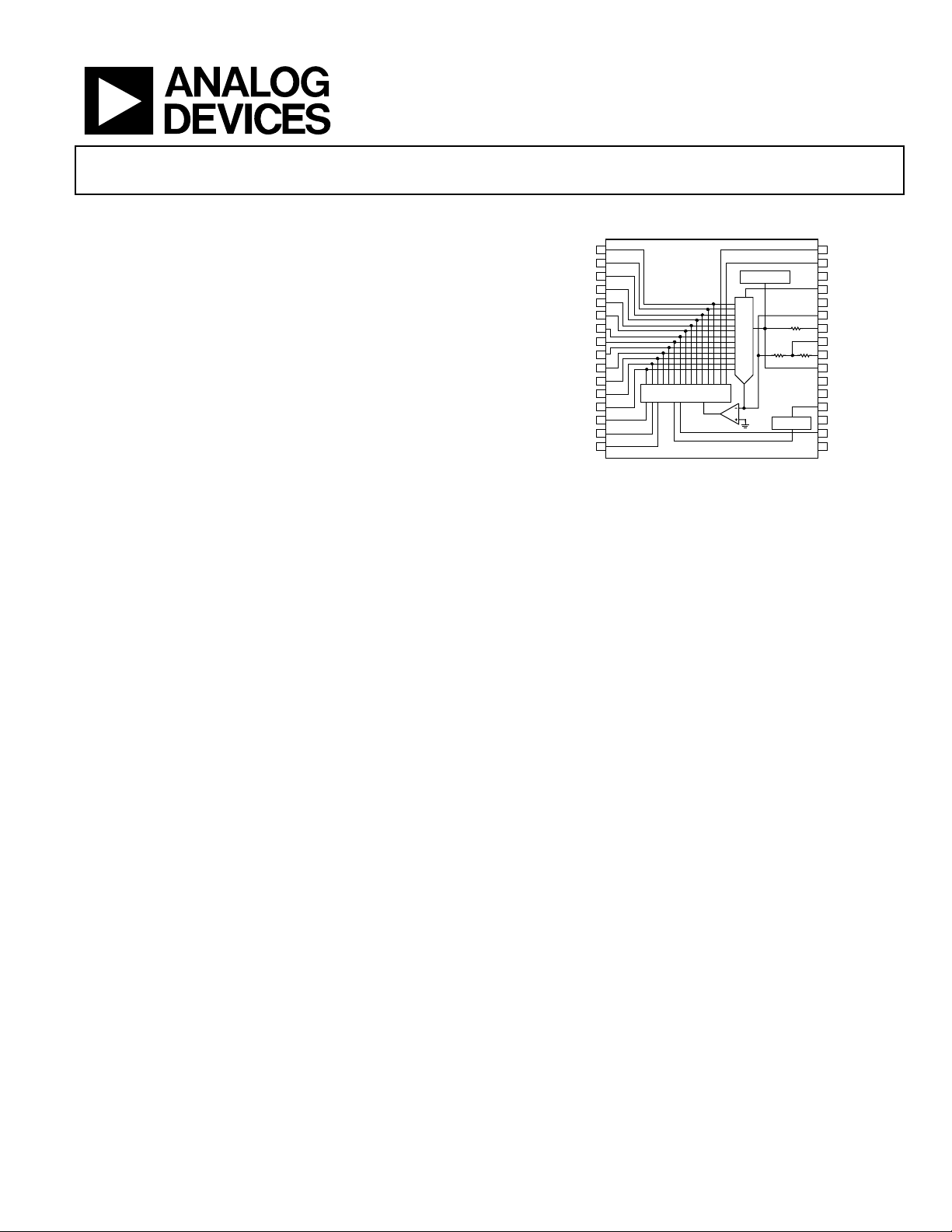
FUNCTIONAL BLOCK DIAGRAM
(MSB) BIT 1
1
BIT 2
BIT 3
BIT 4
BIT 5
BIT 6
BIT 7
BIT 8
BIT 9
BIT 10
BIT 11
BIT 12
(LSB FOR 13 BITS) BIT 13
(LSB FOR 14 BITS) BIT 14
BIT 15
BIT 16
2
3
4
5
6
7
8
9
10
11
12
13
14
15
16
NC = NO CONNECT
ADADC71
16-BIT SAR
COMPARATOR
REFERENCE
3.75kΩ 3.75kΩ
16-BIT DAC
CLOCK
Figure 1.
PRODUCT HIGHLIGHTS
1. The ADADC71 provides 16-bit resolution with a
maximum linearity error less than ±0.003% (±0.006% for
J grades) at 25
2. Conversion time is 35 μs typical (50 μs max) to 14 bits with
short cycle capability.
3. Two binary codes are available on the ADADC71 output:
complementary straight binary (CSB) for unipolar input
voltage ranges, and complementary offset binary (COB) for
bipolar input ranges. Complementary two’s complement
(CTC) coding may be obtained by inverting Pin 1 (MSB).
4. The proprietary chips used in this hybrid design provide
excellent stability over temperature, and lower chip count
for improved reliability.
o
C.
7.5kΩ
SHORT CYCLE
32
CONVERT COMMAND
31
+5V DC SUPPLY V
30
GAIN ADJUST
29
+15V DC SUPPLY V
28
COMPARATOR IN
27
26
BIPOLAR OFFSET
+10V
25
+20V
24
REF OUT (4.3V)
23
22
ANALOG COMMON
–15V DC SUPPLY V
21
CLOCK OUT
20
DIGITAL COMMON
19
18
STATUS
NC
17
L
CC
EE
03537-001
Rev. C
Information furnished by Analog Devices is believed to be accurate and reliable.
However, no responsibility is assumed by Analog Devices for its use, nor for any
infringements of patents or other rights of third parties that may result from its use.
Specifications subject to change without notice. No license is granted by implication
or otherwise under any patent or patent rights of Analog Devices. Trademarks and
registered trademarks are the property of their respective owners.
One Technology Way, P.O. Box 9106, Norwood, MA 02062-9106, U.S.A.
Tel: 781.329.4700 www.analog.com
Fax: 781.461.3113 © 2005 Analog Devices, Inc. All rights reserved.

ADADC71
TABLE OF CONTENTS
Specifications..................................................................................... 3
Digital Output Data......................................................................8
Absolute Maximum Ratings............................................................ 5
ESD Caution.................................................................................. 5
Theory of Operation ........................................................................ 6
Description of Operation ................................................................ 7
Gain Adjustment .......................................................................... 7
Zero Offset Adjustment............................................................... 7
Timing............................................................................................ 7
REVISION HISTORY
6/05—Rev. B to Rev. C
Updated Format ..................................................................Universal
Removed ADADC72..........................................................Universal
Updated Outline Dimensions....................................................... 12
Changes to Ordering Guide.......................................................... 12
Input Scaling ..................................................................................8
Calibration (14-Bit Resolution Examples).................................9
Grounding, Decoupling, and Layout Considerations ........... 10
T/H Requirements for High Resolution Applications .......... 10
Using the ADADC71 at Slower Conversion Times ............... 11
Outline Dimensions ....................................................................... 12
Ordering Guide .......................................................................... 12
Rev. C | Page 2 of 12
ADADC71
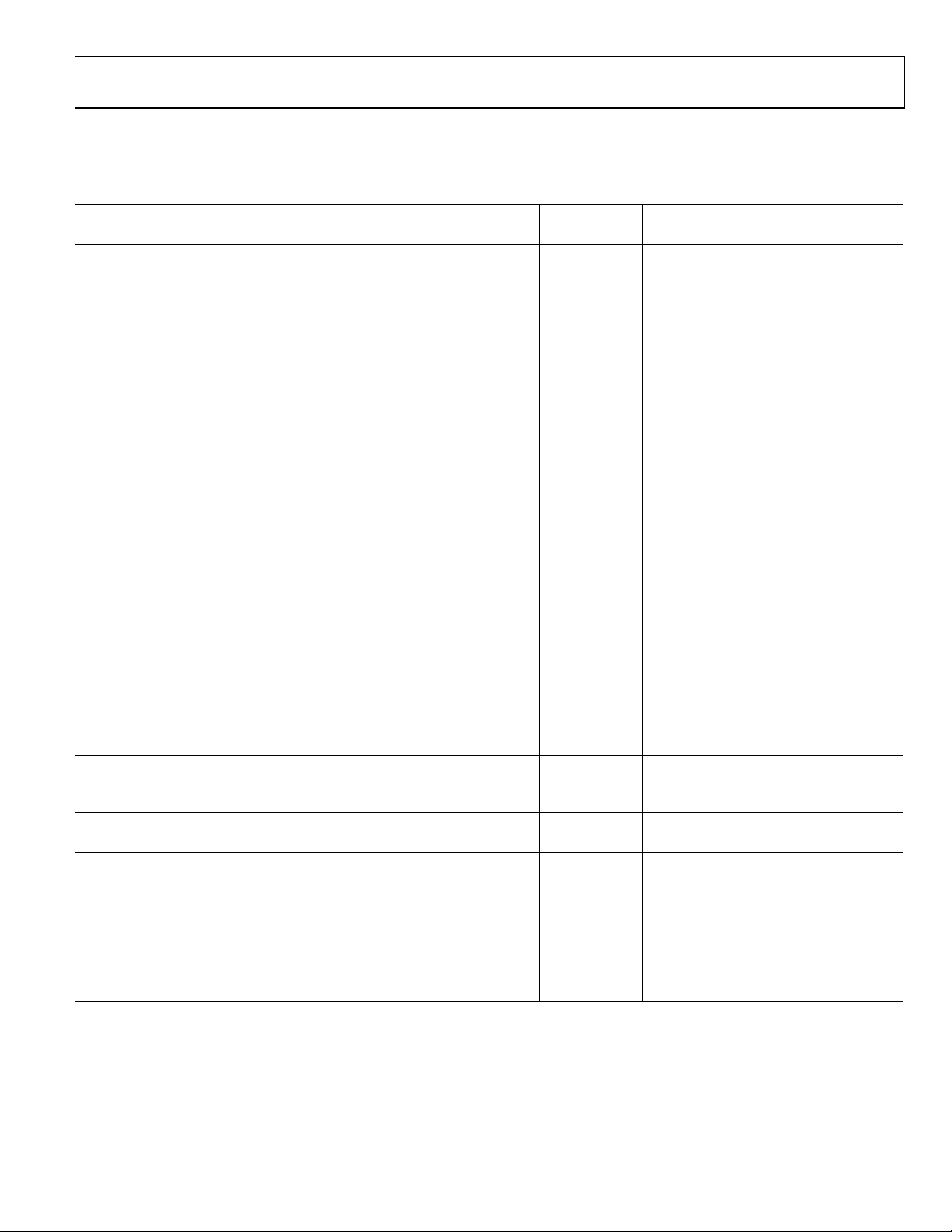
SPECIFICATIONS
Typical at TA =+25oC, VS = ±15 V, +5 V unless otherwise noted.
Table 1.
Parameter Min Typ Max Units Comment
RESOLUTION 16 Bits
ANALOG INPUTS
Voltage Ranges
Bipolar
±5 V
±10 V
Unipolar
Impedance (Direct Input)
0 to ±5 V, ±2.5 V
0 to ±10 V, ±5.0 V
0 to ±20 V, ±10 V
DIGITAL INPUTS
1
Convert command
Logic Loading
TRANSFER CHARACTERISTICS
ACCURACY
Gain Error ±0.1
Offset Error
Unipolar ±0.05
Bipolar ±0.1
Linearity Error ±0.006 % of FSR J Grade
±0.003 % of FSR K Grade
Inherent Quantization Error ±1/2 LSB
Differential Linearity Error ±0.003 % of FSR
No Missing Codes @ 25oC
4
POWER SUPPLY SENSITIVITY
±15 V dc 0.003 % of FSR/%ΔVs
+5 V dc 0.001 % of FSR/%ΔVs
CONVERSION TIME5 (14 BITS) 35 50 μs
WARM-UP TIME 5 Minutes
DRIFT
Gain ±15 ppm/oC
Offset
Unipolar ±2 ±4 ppm of FSR/oC
Bipolar ±10 ppm of FSR/oC
Linearity ±2 ±3 ppm of FSR/oC
Guaranteed No Missing Code
Temperature Range
4
±2.5 V
0 to +5 V
0 to +10 V
0 to +20 V
1.88 KΩ
3.75 KΩ
7.50 KΩ
1 LSTTL Load
2
2
2
±0.2 %
±0.1 % of FSR
3
±0.2 % of FSR
Trailing edge of positive 50 ns (min) pulse
initiates conversion
to 14 bits Guaranteed K Grade
0 to 70
o
C JD (13 bits), KD (14 bits)
Rev. C | Page 3 of 12

ADADC71
Parameter Min Typ Max Units Comment
DIGITAL OUTPUT
Parallel Output Codes
Unipolar CSB
Bipolar COB, CTC
Output Drive 5 LSTTL Loads
Status Logic 1 during conversion
Status Output Drive 5 LSTTL Loads
Internal Clock
Clock Output Drive 5 LSTTL Loads
Frequency 400 kHz
INTERNAL REFERENCE VOLTAGE 6.3 V dc
Error ±5 %
Max External Current Drain with No
Degradation of Specifications
Temperature Coefficient ±10 ppm/oC
POWER SUPPLY REQUIREMENTS
Power Consumption 645 850 mW
Rated Voltage, Analog ±15 ±0.5 V dc
Rated Voltage, Digital ±5 ±0.25 V dc
Supply Drain +15 V dc +16 mA
Supply Drain −15 V dc −21 mA
Supply Drain +5 V dc +18 mA
TEMPERATURE RANGE
Specification 0 to +70 °C
Operating (Derated Specs) −25 to +85 °C
Storage −55 to +125 °C
1
For inputs Logic 0 = 0.8 V, max. Logic 1 = 2.0 V, min. For digital outputs Logic 0 = 0.4 V max. Logic 1 = 2.4 V min.
2
Adjustable to 0.
3
Full scale range.
4
For definition of “No Missing Codes,” refer to the Theory of Operation section.
5
Conversion time may be shortened with short cycle set for lower resolution.
6
CSB—Complementary straight binary. COB— Complementary offset binary, CTC—Complementary twos complement.
7
CTC coding obtained by inverting MSB (Pin 1).
1
6
All codes complementary
7
±200 μA
Rev. C | Page 4 of 12

ADADC71
ABSOLUTE MAXIMUM RATINGS
Table 2.
Parameter Rating
Supply Voltage ±18 V
Logic Supply Voltage 7 V
Analog Ground to Digital Ground ±0.3 V
Analog Inputs (Pin 25, Pin 24) ±V
Digital Input −0.3 V to VDD + 0.3 V
Junction Temperature 175°C
Storage Temperature 150°C
Lead Temperature (Soldering, 10 sec) 300°C
S
Stresses above those listed under Absolute Maximum Ratings
may cause permanent damage to the device. This is a stress
rating only; functional operation of the device at these or any
other conditions above those indicated in the operational
section of this specification is not implied. Exposure to absolute
maximum rating conditions for extended periods may affect
device reliability.
ESD CAUTION
ESD (electrostatic discharge) sensitive device. Electrostatic charges as high as 4000 V readily accumulate on
the human body and test equipment and can discharge without detection. Although this product features
proprietary ESD protection circuitry, permanent damage may occur on devices subjected to high energy
electrostatic discharges. Therefore, proper ESD precautions are recommended to avoid performance
degradation or loss of functionality.
Rev. C | Page 5 of 12

ADADC71
=
∈
=
∈
=
∈
THEORY OF OPERATION
The analog continuum is partitioned into 216 discrete ranges for
16-bit conversion. All analog values within a given quantum are
represented by the same digital code, usually assigned to the
nominal midrange value. An inherent quantization uncertainty
of ±1/2 LSB is associated with the resolution, in addition to the
actual conversion errors.
0.016
0.013
0.006
0.003
–0.003
–0.006
ADADC71
±3ppm/°C,
±0.006%, @ 25°C
0
0.0195
0.0180
0.0150
0
linearity error is based on the DAC resistor ratios. It is
unadjustable and is the most meaningful indication of ADC
accuracy. Differential nonlinearity is a measure of the deviation
in the staircase step width between codes from the ideal least
significant bit step size (
000 ... 000
011 ... 111
OFFSET
ERROR
Figure 4).
–1/2LSB
ALL BITS ON
GAIN
ERROR
+1/2LSB
LINEARITY ERROR (% FSR)
–0.013
–0.016
025 70
TEMPERATURE (°C)
–0.0150
–0.0180
–0.0195
Figure 2. Linearity Error vs. Temperature
0.100
0.038
0
–0.038
GAIN DRIFT ERROR (% FSR)
–0.100
0605040302010
±15ppm/°C
TEMPERATURE (°C)
0.068
0
–0.068
70
Figure 3. Gain Drift Error vs. Temperature
The actual conversion errors associated with ADCs are
combinations of analog errors due to the linear circuitry,
matching and tracking properties of the ladder and scaling
networks, reference error, and power supply rejection. The
matching and tracking errors in the converter have been
minimized by the use of monolithic DACs that include the
scaling network. The initial gain and offset errors are specified
at ±0.2% FSR for gain and ±0.1% FSR for offset. These errors
may be trimmed to 0 by using external trim circuits as shown in
Figure 5 and Figure 6. Linearity error is defined for unipolar
ranges as the deviation from a true straight-line transfer
characteristic from a zero voltage analog input, which calls for a
zero digital output, to a point that is defined as a full scale. The
03537-002
03537-003
DIGITAL OUTPUT (COB CODE)
111 ... 111
ALL BITS OFF
–FS
ANALOG INPUT
0
+FSR – 1LSB
03537-004
Figure 4. Transfer Characteristics for an Ideal Bipolar ADC
Monotonic behavior requires that the differential linearity error
be less than 1 LSB. However, a monotonic converter can have
missing codes. The ADADC71 is specified as having no missing
codes over temperature ranges noted in the
Specifications
section.
There are three types of drift error over temperature: offset, gain
and linearity. Offset drift causes a shift of the transfer
characteristic left or right on the diagram over the operating
temperature range. Gain drift causes a rotation of the transfer
characteristic about the zero point for unipolar ranges or the
negative full-scale point for bipolar ranges. The worst case
accuracy drift is the summation of all three drift errors over
temperature. Statistically, however, the drift error behaves as the
root-sum-square (RSS) and can be shown as
RSS ∈+∈+∈=
OG
222
L
where:
)./( Cppmerrordriftgain
°
G
O
L
)./( CFSRofppmerrordriftoffset
°
)./( CFSRofppmerrorlinearity
°
Rev. C | Page 6 of 12

ADADC71
DESCRIPTION OF OPERATION
On receipt of a CONVERT START command, the ADADC71
converts the voltage at its analog input into an equivalent 16-bit
binary number. This conversion is accomplished as follows: the
16-bit successive-approximation register (SAR) has its 16-bit
outputs connected both to the device bit output pins and to the
corresponding bit inputs of the feedback DAC. The analog
input is successively compared to the feedback DAC output, one
bit at a time (MSB first, LSB last). The decision to keep or reject
each bit is then made at the completion of each bit comparison
period, depending on the state of the comparator at that time.
In either adjustment circuit, the fixed resistor connected to
Pin 27 should be located close to this pin to keep the pin
connection runs short. Pin 27 is quite sensitive to external noise
pick-up.
+15V
10kΩ
OFFSET
ADJ
TO
100kΩ
180kΩ M.F.
–15V
Figure 7. Low Temperature Coefficient Zero Adjustment Circuit
180kΩ M.F.
22kΩ M.F.
27
ADADC71
03537-007
GAIN ADJUSTMENT
The gain adjustment circuit consists of a 100 ppm/oC potentiometer connected across ±V
with its slider connected
S
through a 510 kΩ resistor to Pin 29 (GAIN ADJUST), as shown
in
Figure 5.
If no external trim adjustment is desired, Pin 27
(COMPARATOR IN) and Pin 29 may be left open.
+15V
100ppm/°C
10kΩ
100kΩ
Figure 5. Gain Adjustment Circuit
TO
–15V
270kΩ
0.01μF
29
ADADC71
03537-005
ZERO OFFSET ADJUSTMENT
The zero offset adjustment circuit consists of a 100 ppm/oC
potentiometer connected across ±V
through a 1.8 MΩ resistor to Pin 27 for all ranges. As shown in
Figure 6, the tolerance of this fixed resistor is not critical; a
carbon composition type is generally adequate. Using a carbon
composition resistor with a −1200 ppm/
coefficient contributes a worst-case offset temperature
coefficient of 32 LSB
2.3 ppm/ C of FSR, if the offset adjustment potentiometer is set
o
B
× 61 ppm/ LSB14 × 1200 ppm/ C =
14
at either end of its adjustment range. Since the maximum offset
adjustment required is typically no more than ±16 LSB
a carbon composition offset summing resistor typically
contributes no more than 1 ppm/ C of FSR offset temperature
coefficient.
+15V
TO
1.8MΩ
–15V
10kΩ
100kΩ
Figure 6. Zero Offset Adjustment Circuit
An alternate offset adjustment circuit, which contributes
negligible offset temperature coefficient if metal film resistors
(temperature coefficient < 100 ppm/
Figure 7.
with its slider connected
S
o
C temperature
o
27
ADADC71
03537-006
o
C) are used, is shown in
o
, use of
14
TIMING
The timing diagram is shown in Figure 8. Receipt of a
CONVERT START signal sets the STATUS flag, indicating
conversion in progress. This in turn removes the inhibit applied
to the gated clock, permitting it to run through 17 cycles. All
the SAR parallel bits, STATUS flip-flops, and the gated clock
inhibit signal are initialized on the trailing edge of the
CONVERT START signal. At time t
set unconditionally. At t
the Bit 1 decision is made (keep) and
1
Bit 2 is reset unconditionally. This sequence continues until the
Bit 16 (LSB) decision (keep) is made at t
reset, indicating that the conversion is complete and that the
parallel output data is valid. Resetting the STATUS flag restores
the gated clock inhibit signal, forcing the clock output to the
low Logic 0 state. Note that the clock remains low until the next
conversion.
Corresponding parallel data bits become valid on the same
positive-going clock edge.
(1)
CONVERT
START
INTERNAL
CLOCK
STATUS
t0t1t2t3t4t5t6t7t8t9t10t11t12t13t14t15t
(3)
MSB
BIT 2
BIT 3
BIT 4
BIT 5
BIT 6
BIT 7
BIT 8
BIT 9
BIT 10
BIT 11
BIT 12
BIT 13
BIT 14
BIT 15
LSB
0
1
01 10 01 110 1 1 1 1 0 1 0
NOTES:
1. THE CONVERT START PULSEWIDTH IS 50ns MIN AND MUST REMAIN LOW DURING A
CONVERSION. THE CONVERSION IS INITIATED BY THE TRAILING EDGE OF THE
CONVERT COMMAND.
2. 50μs FOR 14 BITS AND 45μs FOR 13 BITS (MAX).
2. MSB DECISION.
3. CLOCK REMAINS LOW AFTER LAST BIT DECISION.
Figure 8. Timing Diagram (Binary Code 0110011101111010)
MAXIMUM THROUGHPUT TIME
CONVERSION TIME (2)
1
0
0
1
, B1 is reset and B2 to B16 are
0
. The STATUS flag is
16
1
1
0
1
1
1
1
(4)
16
t
17
0
1
0
LSBMSB
03537-008
Rev. C | Page 7 of 12

ADADC71
DIGITAL OUTPUT DATA
Parallel data from TTL storage registers is in negative true form
(Logic 1 = 0 V and Logic 0 = 2.4 V). Parallel data output coding
is complementary binary for unipolar ranges and complementary offset binary for bipolar ranges. Parallel data becomes
valid at least 20 ns before the STATUS flag returns to Logic 0,
permitting parallel data transfer to be clocked on the 1 to 0
transition of the STATUS flag (see
outputs change state on positive-going clock edges.
BIT 16
VALID
BUSY
(STATUS)
Figure 9. LSB Valid to Status Low
Short Cycle Input: Pin 32 (SHORT CYCLE) permits the timing
cycle shown in Figure 8 to be terminated after any number of
desired bits has been converted, allowing somewhat shorter
conversion times in applications not requiring full 16-bit
resolution. When 10-bit resolution is desired, Pin 32 is
connected to Bit 11 output Pin 11. The conversion cycle then
terminates and the STATUS flag resets after the Bit 10 decision
(t
+ 40 ns in the timing diagram of Figure 8). Short cycle
10
connections and associated maximum 8-, 10-, 12-, 13-, 14-, and
15-bit conversion times are summarized in
Table 4. Input Scaling Connections
Input Signal Line Output Code Connect Pin 26 to Connect Pin 24 to
±10 V COB Pin 271 Input Signal Pin 24
±5 V COB Pin 271 Open Pin 25
±2.5 V COB Pin 27
0 V to +5 V CSB Pin 22 Pin 27
0 V to +10 V CSB Pin 22 Open Pin 25
0 V to +20 V CSB Pin 22 Input Signal Pin 24
1
Pin 27 is extremely sensitive to noise and should be guarded by analog common
Table 5. Transition Values vs. Calibration Codes
Output Code
MSB LSB1 Range ±10 V ±5 V ±2.5 V 0 V to +10 V 0 V to +5 V
000. . . .000
2
+Full Scale +10 V +5 V +2.5 V +10 V +5 V
−3/2 LSB −3/2 LSB −3/2 LSB −3/2 LSB −3/2 LSB
011 . . . 111 Mid Scale 0 0 0 +5 V +2.5 V
−1/2 LSB −1/2 LSB −1/2 LSB −1/2 LSB −1/2 LSB
111 . . . 110 −Full Scale −10 V −5 V −2.5 V 0 V 0 V
+1/2 LSB +1/2 LSB +1/2 LSB +1/2 LSB +1/2 LSB
1
For LSB value for range and resolution used, see Table 6.
2
Voltages given are the nominal value for transition to the code specified.
Figure 9). Parallel data
20ns MIN TO 90ns
Tabl e 3.
03537-009
1
Table 3. Short Cycle Connections
Connect Short
Cycle Pin 32
to
Resolution
Bits % FSR
Maximum
Conversion
Time
Status
Flag
Reset
N/C (Open) 16 0.0015 57.0 t16 + 40 ns
Pin 16 15 0.003 53.5 t15 + 40 ns
Pin 15 14 0.006 50.0 t14 + 40 ns
Pin 14 13 0.012 46.5 t13 + 40 ns
Pin 13 12 0.024 42.8 t12 + 40 ns
Pin 11 10 0.100 35.6 t10 + 40 ns
Pin 9 8 0.390 28.5 t8 + 40 ns
INPUT SCALING
The ADADC71 inputs should be scaled as close to the
maximum input signal range as possible in order to utilize the
maximum signal resolution of the ADC. Connect the input
signal as shown in
COMP IN
BIPOLAR
OFFSET
ANALOG
COMMON
1
Pin 27
1
Tabl e 4. See Figure 10 for circuit details.
10V SPAN
25
R2
3.75kΩ
24
27
26
22
20V SPAN
FROM DAC
7.5kΩ
R1
3.75kΩ
V
REF
COMPARATOR
Figure 10. ADADC71 Input Scaling Circuit
For Direct Input,
Connect Input Signal to
Pin 25
Pin 25
TO
SAR
03537-010
Rev. C | Page 8 of 12

ADADC71
k
A
.
k
A
.
Table 6. Input Voltage Range and LSB Values
Analog Input Voltage Range ±10 V ±5 V ±2.5 V 0 V to +10 V 0 V to +5 V
Code Designation COB1 or CTC2 COB1 or CTC
One Least Significant Bit (LSB)
FSR
2
n
V20
n
2
V10
n
2
n = 8 78.13 mV 39.06 mV 19.53 mV 39.06 mV 19.53 mV
n = 10 19.53 mV 9.77 mV 4.88 mV 9.77 mV 4.88 mV
n = 12 4.88 mV 2.44 mV 1.22 mV 2.44 mV 1.22 mV
n = 13 2.44 mV 1.22 mV 0.61 mV 1.22 mV 0.61 mV
n = 14 1.22 mV 0.61 mV 0.31 mV 0.61 mV 0.31 mV
n = 15 0.61 mV 0.31 mV 0.15 mV 0.31 mV 0.15 mV
1
COB = complementary offset binary.
2
CTC = complementary twos complement—achieved by using an inverter to complement the most significant bit to produce (MSB).
3
CSB = complementary straight binary.
KEEP/
IN
REJECT
A
ADADC71
e
IN
(0V TO +10V)
03537-011
+15V
10kΩ
TO
Ω
100
–15V
NOTE:
NALOG ( ) AND DIGITAL ( ) GROUNDS ARE NOT TIED INTERNALLY AND MUST BE CONNECTED EXTERNALLY
+15V
–15V
270kΩ
GAIN
ADJ
0.01μF
23
REF
29
CONTROL
28
+
1μF
22
+
1μF
21
IOS = 1.3mA
30
+5V
+
1μF
APPROMIXATION REGISTER
7.5kΩ
27
+15V
10kΩ
TO
ZERO
100kΩ
ADJ
–15V
16-BIT SUCCESSIVE
16-BIT DAC
3.75kΩ3.75kΩ
I
242619
25
1.8MΩ
Figure 11. Analog and Power Connections
for Unipolar 0 V to +10 V Input Range
KEEP/
+15V
10kΩ
TO
Ω
100
–15V
NOTE:
NALOG ( ) AND DIGITAL ( ) GROUNDS ARE NOT TIED INTERNALLY AND MUST BE CONNECTED EXTERNALLY
+15V
–15V
270kΩ
GAIN
ADJ
0.01μF
23
REF
29
CONTROL
28
+
1μF
22
+
1μF
21
IOS = 1.3mA
30
+5V
+
1μF
APPROMIXATION REGISTER
7.5kΩ
27
+15V
10kΩ
TO
ZERO
100kΩ
ADJ
–15V
16-BIT SUCCESSIVE
16-BIT DAC
3.75kΩ3.75kΩ
I
IN
242619
25
1.8MΩ
REJECT
A
ADADC71
e
IN
(–10V TO +10V)
03537-012
Figure 12. Analog and Power Connections
for Bipolar −10 V to +10 V Input Range
CALIBRATION (14-BIT RESOLUTION EXAMPLES)
External zero adjustment and gain adjustment potentiometers,
connected as shown in
device calibration. To prevent interaction of these two
adjustments, zero is always adjusted first and then gain. Zero is
adjusted with the analog input near the most negative end of the
analog range (0 for unipolar and −FS for bipolar input ranges).
Figure 5 and Figure 6, are used for
2
COB1 or CTC
V5
n
2
2
CSB
3
V10
n
2
CSB3
V5
n
2
Gain is adjusted with the analog input near the most positive
end of the analog range.
0 V to +10 V Range
Set the analog input to +1 LSB14 = 0.00061 V. Adjust zero for
digital output = 11111111111110. Zero is now calibrated. Set
analog input to +FSR − 2 LSB = +9.9987 V. Adjust gain for
00000000000001 digital output code; full-scale (gain) is now
calibrated. Half-scale calibration check: set analog input to
+5.00000 V; digital output code should be 01111111111111.
−10 V to +10 V Range
Set the analog input to −9.99878 V; adjust zero for
11111111111110 digital output (complementary offset binary)
code. Set analog input to 9.99756 V; adjust gain for
00000000000001 digital output (complementary offset binary)
code. Half-scale calibration check: set analog input to 0.00000
V; digital output (complementary offset binary) code should be
01111111111111.
Other Ranges
Representative digital coding for 0 to +10 V and −10 V to +10 V
ranges is given above. Coding relationships and calibration
points for 0 to +5 V, −2.5 V to +2.5 V and −5 V to +5 V ranges
can be found by proportionally halving the corresponding code
equivalents listed for the 0 to +10 V and −10 V to +10 V ranges,
respectively, as indicated in
Tabl e 5.
Zero and full-scale calibration can be accomplished to a
precision of approximately ±1/2 LSB using the static adjustment
procedure described above. By summing a small sine or
triangular wave voltage with the signal applied to the analog
input, the output can be cycled through each of the calibration
codes of interest to more accurately determine the center (or
end point) of each discrete quantization level. A detailed
description of this dynamic calibration technique is presented
A/D Conversion Handbook, D. Sheingold, Analog Devices,
in
Inc., 1986 Part II, Chapter 4.
Rev. C | Page 9 of 12

ADADC71
GROUNDING, DECOUPLING, AND LAYOUT
CONSIDERATIONS
Many data-acquisition components have two or more ground
pins, which are not connected together within the device. These
grounds are usually referred to as the DIGITAL COMMON
(logic power return), ANALOG COMMON (analog power
return), or analog signal ground. These grounds (Pin 19 and
Pin 22) must be tied together at one point as close as possible to
the converter. Ideally, a single solid analog ground plane under
the converter would be desirable. Current flows through the
wires and etch stripes of the circuit card, and since these paths
have resistance and inductance, hundreds of millivolts can be
generated between the system analog ground point and the
ground pins of the ADADC71. Separate wide conductor stripe
ground returns should be provided for high resolution
converters to minimize noise and IR losses from the current
flow in the path from the converter to the system ground point.
In this way the ADADC71 supply currents and other digital
logic-gate return currents are not summed into the same return
path as analog signals where they would cause measurement
errors.
Each of the ADADC71’s supply terminals should be capacitively
decoupled as close to the ADADC71 as possible. A large value,
such as 1 μF, capacitor in parallel with a 0.1 μF capacitor is
usually sufficient. Analog supplies are to be bypassed to the
ANALOG COMMON (analog power return) Pin 22 and the
logic supply is bypassed to DIGITAL COMMON (logic power
return) Pin 19.
The T/H amplifier slew rate determines the maximum
frequency tracking rate and part of the settling time when
sampling pulses and square waves. The feedthrough from input
to output while in the hold mode should be less than 1 LSB. The
amplitude of 1 LSB of the companion ADC for a given input
range will vary from 610 μV for a 14-bit ADC using a 0 V to
+10 V input range to 4.88 mV for a 12-bit ADC using a ±10 V
input range. The hold mode droop rate should produce less
than 1 LSB of droop in the output during the conversion time of
the ADC. For 610 μV/LSB, as noted in the example above, for a
50 μs 14-bit ADC, the maximum droop rate is 610 μV/50 μs or
12 μV/μs during the 50 μs conversion period.
Minimal thermal tail effects are another requirement of high
resolution applications. The self-heating errors induced by the
changing current levels in the output stages of T/H amps may
cause more than 1 LSB of error due to thermal tail effects.
The linearity error should be less than 1 LSB over the transfer
function, as set by the resolution of the ADC. The T/H
acquisition time and T/H settling time along with the
conversion time of the ADC determines the highest sampling
rate. This in turn determines the highest input signal frequency
that can be sampled at twice a cycle.
The maximum input frequency is constrained by the Nyquist
sampling theorem to be half of the maximum throughput rate.
Input frequencies higher than half the maximum throughput
rate result in under sampling or aliasing errors of the input
signal.
The metal cover is internally grounded with respect to the
power supplies, grounds and electrical signals. Do not
externally ground the cover.
T/H REQUIREMENTS FOR HIGH RESOLUTION APPLICATIONS
The characteristics required for high resolution track-and-hold
amplifiers are low feedthrough, low pedestal shifts with changes
of input signal or temperature, high linearity, low temperature
coefficients, and minimal droop rate.
The aperture jitter is a result of noise within the switching
network that modulates the phase of the hold command, and is
manifested in the variations in the value of the analog input that
has been held. The aperture error which results from this jitter
is directly related to the dV/dt of the analog input.
The pedestal shift due to input signal changes should either be
linear, to be seen as a gain error, or negligible, as with the
feedthrough specification. The temperature coefficients for drift
would be low enough such that full accuracy is maintained over
some minimum temperature range. The droop rate and
pedestal shift increases above +70
and industrial users, these shifts only appear above the highest
temperatures their equipment might expect to experience. Most
precision instrumentation is installed only in human
inhabitable work spaces or in controlled enclosures if the area
has a hostile environment. Thus, the ADADC71 used with a
sample-and-hold amplifier offers high accuracy sampling in
high precision applications.
o
C (+158oF). For commercial
Rev. C | Page 10 of 12

ADADC71
USING THE ADADC71 AT SLOWER CONVERSION
TIMES
The user may wish to run the ADADC71 at slower conversion
times in order to synchronize the ADC with an external clock.
This is accomplished by running a slower clock that the internal
clock into the START CONVERT input. This clock must consist
of narrow negative-going clock pulses, as seen in
pulse must be a minimum of 100 ns wide, but not greater than
700 ns. Having a raising edge immediately after a falling edge
inhibits the internal clock pulse. This enables the ADADC71 to
function normally and complete a conversion after 16 clock
pulses. The STATUS command functions normally and
switches high after the first clock pulse and falls low after the
th
clock pulse. In this way an external clock can be used to
17
control the ADADC71 at slower conversion times.
Figure 13. The
START CONVERT
(EXTERNAL CLOCK)
CLOCK OUT
STATUS
Figure 13. Timing Diagram for Use with an External Clock
100ns MIN
1500ns MAX
t
0
NOTE:
1
EXTENAL CLK RATE CTRL (PIN 23) GROUNDED.
1
t
1
t
t
15
16
03537-013
Rev. C | Page 11 of 12

ADADC71
OUTLINE DIMENSIONS
1.728 (43.89) MAX
1732
1.102 (27.99)
1.079 (27.41)
16
0.025 (0.64)
0.015 (0.38)
0.206 (5.23)
0.186 (4.72)
0.120 (3.05)
MAX
0.910 (23.11)
0.890 (22.61)
0.015 (0.38)
0.008 (0.20)
0.225 (5.72)
MAX
0.192 (4.88)
0.152 (3.86)
0.025 (0.64)
1
PIN 1
INDICATOR
(NOTE 1)
MIN
0.023 (0.58)
0.014 (0.36)
0.100 (2.54)
BSC
0.070 (1.78)
0.030 (0.76)
NOTES:
1. INDEX AREA IS INDICATED BY A NOTCH OR LEAD ONE
IDENTIFICATION MARK LOCATED ADJACENT TO LEAD ONE.
2. CONTROLLING DIMENSIONS ARE IN INCHES; MILLIMETER DIMENSIONS
(IN PARENTHESES) ARE ROUNDED-OFF INCH EQUIVALENTS FOR
REFERENCE ONLY AND ARE NOT APPROPRIATE FOR USE IN DESIGN.
Figure 14. 32-Lead Bottom-Brazed Ceramic Dip for Hybrid [BBDIP_H]
(DH-32E)
Dimensions shown in inches and (millimeters)
ORDERING GUIDE
Model Linearity Error (Max) Specification Temp Range Package Option
AD ADC71JD ±0.006% of FSR 0°C to +70°C Ceramic (DH-32E)
AD ADC71KD ±0.003% of FSR 0°C to +70°C Ceramic (DH-32E)
© 2005 Analog Devices, Inc. All rights reserved. Trademarks and
registered trademarks are the property of their respective owners.
C03537–0–6/05(C)
Rev. C | Page 12 of 12
 Loading...