

Fully Differential ADC Driver
ADA4940-1/ADA4940-2
Rev. B
Information furnished by Analog Devices is believed to be accurate and reliable. However, no
Trademarks and registered trademarks are the property of their respective owners.
Fax: 781.461.3113 ©2011–2012 Analog Devices, Inc. All rights reserved.
1–FB
2+IN
3–IN
4+FB
11 –OUT
12 DISABLE
10 +OUT
9 V
OCM
5+V
S
6+V
S
7+V
S
8
+V
S
15
–V
S
16
–V
S
14
–V
S
13
–V
S
ADA4940-1
08452-001
ADA4940-2
1–IN1
2+FB1
3+V
S1
4+V
S1
5–FB2
6+IN2
15
–V
S2
16 –V
S2
17 V
OCM1
18 +OUT1
14
DISABLE2
13 –OUT2
7–IN2
8+FB2
9+V
S2
11V
OCM2
12+OUT2
10+V
S2
21
–V
S1
22
–V
S1
23
–FB1
24
+IN1
20
DISABLE1
19
–OUT1
0
–160
–140
–120
–100
–80
–60
–40
–20
0 20k 40k 60k 80k 100k
08452-300
AMPLIT UDE ( dB)
FREQUENCY ( Hz )
+D
IN
–D
IN
R1 R2
R4R3
+IN
–OUT
C
F
33Ω
2.5V
AD7982
ADA4940-1
33Ω
2.7nF
2.7nF
C
F
+OUT
+
–
–IN
IN+
IN–
GND
VDDREF
V
OCM
AD7621
65 3 16
88
Data Sheet
FEATURES
Small signal bandwidth: 260 MHz
Ultralow power 1.25mA
Extremely low harmonic distortion
−122 dB THD at 50 kHz
−96 dB THD at 1 MHz
Low input voltage noise: 3.9 nV/√Hz
0.35 mV maximum offset voltage
Balanced outputs
Settling time to 0.1%: 34 ns
Rail-to-rail output: −V
Adjustable output common-mode voltage
Flexible power supplies: 3 V to 7 V (LFCSP)
Disable pin to reduce power consumption
ADA4940-1 is available in LFCSP and SOIC packages
APPLICATIONS
Low power PulSAR®/SAR ADC drivers
Single-ended-to-differential conversion
Differential buffers
Line drivers
Medical imaging
Industrial process controls
Portable electronics
+ 0.1 V to +VS − 0.1 V
S
Ultralow Power, Low Distortion
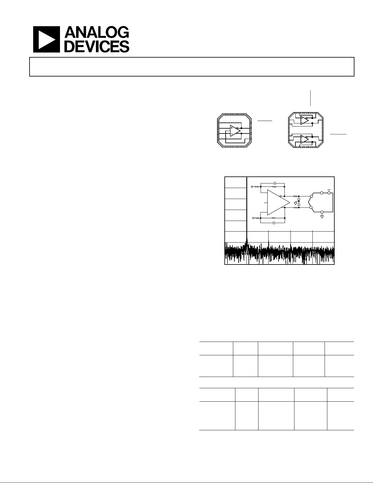
FUNCTIONAL BLOCK DIAGRAMS
Figure 1.
GENERAL DESCRIPTION
The ADA4940-1/ADA4940-2 are low noise, low distortion fully
differential amplifiers with very low power consumption. They
are an ideal choice for driving low power, high resolution, high
performance SAR and sigma-delta (Σ-Δ) analog-to-digital
converters (ADCs) with resolutions up to 16 bits from dc to
1 MHz on only 1.25 mA of quiescent current. The adjustable
level of the output common-mode voltage allows the ADA4940-1/
ADA4940-2 to match the input common-mode voltage of
multiple ADCs. The internal common-mode feedback loop
provides exceptional output balance, as well as suppression of
even-order harmonic distortion products.
With the ADA4940-1/ADA4940-2, differential gain configurations
are easily realized with a simple external feedback network of
four resistors determining the closed-loop gain of the amplifier.
The ADA4940-1/ADA4940-2 are fabricated using Analog Devices,
Inc., SiGe complementary bipolar process, enabling them to
achieve very low levels of distortion with an input voltage noise
of only 3.9 nV/√Hz. The low dc offset and excellent dynamic
performance of the ADA4940-1/ADA4940-2 make them well
suited for a variety of data acquisition and signal processing
applications.
responsibility is assumed by Analog Devices for its use, nor for any infringements of patents or other
rights of third parties that may result from its use. Specifications subject to change without notice. No
license is granted by implication or otherwise under any patent or patent rights of Analog Devices.
Figure 2. ADA4940-1 Driving the AD7982 ADC
The ADA4940-1 is available in a Pb-free, 3 mm × 3 mm, 16-lead
LFCSP, and an 8-lead SOIC. The ADA4940-2 is available in a Pb-
free, 4 mm × 4 mm, 24-lead LFCSP. The pinout is optimized to
facilitate printed circuit board (PCB) layout and minimize
distortion. The ADA4940-1/ADA4940-2 are specified to
operate over the −40°C to +125°C temperature range.
Table 1. Similar Products to the ADA4940-1/ADA4940-2
Product
(mA)
AD8137 3 110 450 8.25
ADA4932-x 9 560 2800 3.6
ADA4941-1 2.2 31 22 5.1
Isupply
Bandwidth
(MHz)
Slew Rate
(V/µs)
Table 2. Complementary Products to the ADA4940-1/ADA4940-2
Product
(mW)
AD7982 7.0 1 18 98
AD7984 10.5 1.333 18 96.5
AD7623 45 1.333 16 88
One Technology Way, P.O. Box 9106, Norwood, MA 02062-9106, U.S.A.
Tel: 781.329.4700
Power
Throughput
(MSPS)
Resolution
(Bits)
www.analog.com
Noise
(nV/√Hz)
SNR
(dB)

ADA4940-1/ADA4940-2 Data Sheet
TABLE OF CONTENTS
Features .............................................................................................. 1
Applications ....................................................................................... 1
General Description ......................................................................... 1
Functional Block Diagrams ............................................................. 1
Revision History ............................................................................... 2
Specifications ..................................................................................... 3
VS = 5 V .......................................................................................... 3
VS = 3 V .......................................................................................... 5
Absolute Maximum Ratings ............................................................ 7
Thermal Resistance ...................................................................... 7
Maximum Power Dissipation ..................................................... 7
ESD Caution .................................................................................. 7
Pin Configurations and Function Descriptions ........................... 8
Typical Performance Characteristics ........................................... 10
Test Circuits ..................................................................................... 19
Terminology .................................................................................... 20
Definition of Terms .................................................................... 20
Theory of Operation ...................................................................... 21
Applications Information .............................................................. 22
Analyzing an Application Circuit ............................................ 22
Setting the Closed-Loop Gain .................................................. 22
Estimating the Output Noise Voltage ...................................... 22
Impact of Mismatches in the Feedback Networks ................. 23
Calculating the Input Impedance of an Application Circuit 23
Input Common-Mode Voltage Range ..................................... 24
Input and Output Capacitive AC Coupling ............................ 25
Setting the Output Common-Mode Voltage .......................... 25
DISABLE
Pin .............................................................................. 25
Driving a Capacitive Load ......................................................... 25
Driving a High Precision ADC ................................................ 26
Layout, Grounding, and Bypassing .............................................. 27
ADA4940-1 LFCSP Example .................................................... 27
Outline Dimensions ....................................................................... 28
Ordering Guide .......................................................................... 29
REVISION HISTORY
3/12—Rev. A to Rev. B
Reorganized Layout ............................................................ Universal
Added ADA4940-1 8-Lead SOIC Package ...................... Universal
Changes to Features Section, Table 1, and Figure 1; Replaced
Figure 2 .............................................................................................. 1
Changed V
Section ................................................................................................ 3
Changes to V
Changes to Table 4 and Table 5 ....................................................... 4
Changes to V
Changes to Table 7 and Table 8 ....................................................... 6
Added Figure 5 and Table 12, Renumbered Sequentially ........... 9
Changes to Figure 7, Figure 8, and Figure 9................................ 10
Added Figure 15 and Figure 18; Changes to Figure 13,
Figure 14, and Figure 16 ................................................................ 11
Changes to Figure 19 and Figure 20 ............................................. 12
Changes to Figure 25, Figure 26, and Figure 27; Added
Figure 28, Figure 29, and Figure 30 .............................................. 13
Changes to Figure 31, Figure 32, Figure 33, Figure 34, Figure 35,
and Figure 36 ................................................................................... 14
Changes to Figure 37, Figure38, Figure 39, and Figure 41 ........ 15
Changes to Figure 49, Figure 50, and Figure 51 ......................... 17
Added Figure 55 and Figure 57..................................................... 18
Changes to Differential V
CMRR Section ................................................................................ 20
Changes to Calculating the Input Impedance of an Application
= ±2 V(or +5 V) Section to VS = +5 V
S
= +5 V Section and Table 3.................................... 3
S
= 3 V Section and Table 6 ...................................... 5
S
, Differential CMRR, and V
OS
OCM
Rev. B | Page 2 of 32
Circuit Section ................................................................................ 23
Changes to Figure 71 ...................................................................... 25
Changes to Driving a High Precision ADC Section
and Figure 73 ................................................................................... 26
Changed ADA4940-1 Example Section to ADA4940-1 LFCSP
Example Section ............................................................................. 27
Changes to Ordering Guide .......................................................... 29
12/11—Rev. 0 to Rev. A
Changes to Features Section, General Description
Section, Table 1 .................................................................................. 1
Replaced Figure 1 and Figure 2 ....................................................... 1
Changes to V
= ±2.5 V (or +5 V) Section and Table 3 ................ 3
S
Changes to Table 6 ............................................................................. 5
Replaced Figure 7, Figure 8, Figure 9, and Figure 10 ................... 9
Replaced Figure 14, Figure 15, and Figure 17 ............................. 10
Replaced Figure 24 and Figure 27 ................................................ 12
Changes to Figure 37 ...................................................................... 14
Replaced Figure 43 and Figure 46 ................................................ 15
Replaced Figure 53 ......................................................................... 18
Changes to Estimating the Output Noise Voltage Section, Table
14, Table 15, and Calculating the Input Impedance of an
Application Circuit Section ........................................................... 21
Changes to Input Common-Mode Voltage Range Section....... 22
Changes to Driving a High Precision ADC Section and
Figure 65 .......................................................................................... 24
10/11—Revision 0: Initial Version

Data Sheet ADA4940-1/ADA4940-2
Input Offset Voltage Drift
T
to T
1.2 µV/°C
Input Resistance
Differential
33 kΩ
Linear Output Current
f = 1 MHz, R
= 22 Ω, SFDR = −60 dBc
46 mA peak
SPECIFICATIONS
VS = 5 V
V
= Mid Supply, RF = RG = 1 kΩ, R
OCM
(See Figure 61 for the definition of terms.)
+DIN or –DIN to V
Performance
OUT, dm
Table 3.
Parameter Test Conditions/Comments Min Typ Max Unit
DYNAMIC PERFORMANCE
−3 dB Small Signal Bandwidth V
V
V
−3 dB Large Signal Bandwidth V
V
V
Bandwidth for 0.1 dB Flatness V
Slew Rate V
Settling Time to 0.1% V
Overdrive Recovery Time G = 2, V
NOISE/HARMONIC PERFORMANCE
HD2/HD3 V
V
V
V
V
IMD3 V
Input Voltage Noise f = 100 kHz 3.9 nV/√Hz
Input Current Noise f = 100 kHz 0.81 pA/√Hz
Crosstalk V
INPUT CHARACTERISTICS
Input Offset Voltage VIP = VIN = V
Input Bias Current −1.6 −1.1 µA
Input Bias Current Drift T
Input Offset Current −500 ±50 +500 nA
Input Common-Mode Voltage Range −VS − 0.2 to
= 1 kΩ, TA = 25°C, LFCSP package, unless otherwise noted. T
L, dm
= 0.1 V p-p, G = 1 260 MHz
OUT, dm
= 0.1 V p-p, G = 2 220 MHz
OU T, dm
= 0.1 V p-p, G = 5 75 MHz
OU T, dm
= 2 V p-p, G = 1 25 MHz
OUT, dm
= 2 V p-p, G = 2 22 MHz
OU T, dm
= 2 V p-p, G = 5 19 MHz
OU T, dm
= 2 V p-p, G = 1 and G = 2 14.5 MHz
OUT, dm
= 2 V step 95 V/µs
OUT, dm
= 2 V step 34 ns
OUT, dm
= 6 V p-p, triangle wave 86 ns
IN, dm
= 2 V p-p, fC = 10 kHz −125/−118 dBc
OU T, dm
= 2 V p-p, fC = 50 kHz −123/−126 dBc
OU T, dm
= 2 V p-p, fC = 50 kHz, G = 2 −124/−117 dBc
OU T, dm
= 2 V p-p, fC = 1 MHz −102/−96 dBc
OUT, dm
= 2 V p-p, fC = 1 MHz, G = 2 −100/–92 dBc
OU T, dm
= 2 V p-p, f1 = 1.9 MHz, f2 = 2.1 MHz −99 dBc
OUT, dm
= 2 V p-p, fC = 1 MHz −110 dB
OUT, dm
MIN
MIN
= 0 V
OCM
MAX
to T
−4.5 nA/°C
MAX
−0.35 ±0.06 +0.35 mV
MIN
+V
to T
= −40°C to +125°C.
MAX
− 1.2
S
V
Common mode 50 MΩ
Input Capacitance 1 pF
Common-Mode Rejection Ratio (CMRR) ΔV
Open-Loop Gain 91 99 dB
OUTPUT CHARACTERISTICS
Output Voltage Swing Each single-ended output −VS + 0.1 to
Output Balance Error f = 1 MHz, ΔV
OS, dm
/ΔV
IN, cm
L, dm
, ∆V
OU T, c m
= ±1 V dc 86 119 dB
IN, cm
/ΔV
Rev. B | Page 3 of 32
−65 −60 dB
OUT, dm
+V
− 0.1
S
−V
+ 0.07 to
S
− 0.07
+V
S
V
ADA4940-1/ADA4940-2 Data Sheet
Parameter
Test Conditions/Comments
Min
Typ
Max
Unit
Quiescent Current Drift
T
to T
4.25 µA/°C
V
to V
OCM
Table 4.
V
DYNAMIC PERFORMANCE
OCM
−3 dB Small Signal Bandwidth V
−3 dB Large Signal Bandwidth V
Slew Rate V
Input Voltage Noise f = 100 kHz 83 nV/√Hz
Gain ΔV
V
CHARACTERISTICS
OCM
Input Common-Mode Voltage Range −VS + 0.8 to
Input Resistance 250 kΩ
Offset Voltage V
Input Offset Voltage Drift T
Input Bias Current −7 +4 +7 µA
CMRR ΔV
General Performance
Table 5.
Parameter Test Conditions/Comments Min Typ Max Unit
POWER SUPPLY
Operating Range LFCSP 3 7 V
SOIC 3 6 V
Quiescent Current per Amplifier Enabled 1.05 1.25 1.38 mA
Disabled 13.5 28.5 µA
+PSRR ΔV
−PSRR ΔV
DISABLE (
DISABLE
Enabled ≥(−VS + 1.8) V
Turn-Off Time 10 µs
Turn-On Time 0.6 µs
DISABLE
Enabled
Disabled
OPERATING TEMPERATURE RANGE −40 +125 °C
Performance
OUT, cm
= 0.1 V p-p 36 MHz
OU T, cm
= 1 V p-p 29 MHz
OU T, cm
= 1 V p-p 52 V/µs
OU T, cm
/ΔV
, ΔV
OU T, c m
OCM
= ±1 V 0.99 1 1.01 V/V
OCM
V
+V
− 0.7
S
DISABLE
= V
OS, cm
to T
MIN
OS, dm
MIN
OS, dm
OS, dm
PIN)
− V
OU T, c m
20 µV/°C
MAX
/ΔV
OCM
MAX
; VIP = VIN = V
OCM
, ΔV
= ±1 V 86 100 dB
OCM
= 0 V −6 ±1 +6 mV
OCM
/ΔVS, ΔVS = 1 V p-p 80 90 dB
/ΔVS, ΔVS = 1 V p-p 80 96 dB
Input Voltage Disabled ≤(−VS + 1) V
Pin Bias Current per Amplifier
DISABLE
DISABLE
= +2.5 V 2 5 µA
= −2.5 V −10 −5 µA
Rev. B | Page 4 of 32

Data Sheet ADA4940-1/ADA4940-2
V
= 0.1 V p-p, G = 5
70 MHz
Crosstalk
V
= 2 V p-p, fC = 1 MHz
−110
dB
Open-Loop Gain
91
99 dB
Linear Output Current
f = 1 MHz, R
= 26 Ω, SFDR = −60 dBc
38 mA peak
VS = 3 V
V
= Mid Supply, RF = RG = 1 kΩ, R
OCM
(See Figure 61 for the definition of terms.)
+DIN or –DIN to V
Performance
OUT, dm
Table 6.
Parameter Test Conditions/Comments Min Typ Max Unit
DYNAMIC PERFORMANCE
−3 dB Small Signal Bandwidth V
V
−3 dB Large Signal Bandwidth V
V
V
Bandwidth for 0.1 dB Flatness V
Slew Rate V
Settling Time to 0.1% V
Overdrive Recovery Time G = 2, V
NOISE/HARMONIC PERFORMANCE
HD2/HD3 V
V
IMD3 V
Input Voltage Noise f = 100 kHz 3.9 nV/√Hz
Input Current Noise f = 100 kHz 0.84 pA/√Hz
INPUT CHARACTERISTICS
Input Offset Voltage VIP = VIN = V
Input Offset Voltage Drift T
Input Bias Current −1.6 −1.1 µA
Input Bias Current Drift T
Input Offset Current −500 ±50 +500 nA
Input Common-Mode Voltage Range −VS − 0.2 to
Input Resistance Differential 33 kΩ
Common mode 50 MΩ
Input Capacitance 1 pF
Common-Mode Rejection Ratio (CMRR) ΔV
= 1 kΩ, TA = 25°C, LFCSP package, unless otherwise noted. T
L, dm
= 0.1 V p-p 240 MHz
OU T, dm
= 0.1 V p-p, G = 2 200 MHz
OU T, dm
OU T, dm
= 2 V p-p 24 MHz
OU T, dm
= 2 V p-p, G = 2 20 MHz
OU T, dm
= 2 V p-p, G = 5 17 MHz
OU T, dm
= 0.1 V p-p 14 MHz
OU T, dm
= 2 V step 90 V/µs
OU T, dm
= 2 V step 37 ns
OU T, dm
= 3.6 V p-p, triangle wave 85 ns
IN, dm
= 2 V p-p, fC = 50 kHz (HD2/HD3) −115/−121 dBc
OU T, dm
= 2 V p-p, fC = 1 MHz (HD2/HD3) −104/−96 dBc
OU T, dm
= 2 V p-p, f1 = 1.9 MHz, f2 = 2.1 MHz −98 dBc
OU T, dm
OU T, dm
MIN
MIN
= 1.5 V
OCM
to T
1.2 µV/°C
MAX
to T
−4.5 nA/°C
MAX
/ΔV
OS, dm
IN, cm
, ∆V
= ±0.25 V dc 86 114 dB
IN, cm
−0.4 ±0.06 +0.4 mV
MIN
+V
to T
= −40°C to +125°C.
MAX
− 1.2
S
V
OUTPUT CHARACTERISTICS
Output Voltage Swing Each single-ended output −VS + 0.08 to
Output Balance Error f = 1 MHz, ΔV
L, dm
/ΔV
OU T, c m
Rev. B | Page 5 of 32
+ 0.04 to
−V
+V
− 0.08
S
−65 −60 dB
OUT, dm
+V
S
− 0.04
S
V
ADA4940-1/ADA4940-2 Data Sheet
Parameter
Test Conditions/Comments
Min
Typ
Max
Unit
SOIC 3 6 V
V
to V
OCM
Table 7.
V
DYNAMIC PERFORMANCE
OCM
−3 dB Small Signal Bandwidth V
−3 dB Large Signal Bandwidth V
Slew Rate V
Input Voltage Noise f = 100 kHz 92 nV/√Hz
Gain ΔV
V
CHARACTERISTICS
OCM
Input Common-Mode Voltage Range −VS + 0.8 to
Input Resistance 250 kΩ
Offset Voltage V
Input Offset Voltage Drift T
Input Bias Current −5 +1 +5 µA
CMRR ΔV
General Performance
Performance
OUT, cm
= 0.1 V p-p 36 MHz
OU T, cm
= 1 V p-p 26 MHz
OU T, cm
= 1 V p-p 48 V/µs
OU T, cm
/ΔV
, ΔV
OU T, c m
OCM
= ±0.25 V 0.99 1 1.01 V/V
OCM
V
+V
− 0.7
S
OS, cm
MIN
OS,dm
= V
to T
− V
OU T, c m
20 µV/°C
MAX
/ΔV
, ΔV
OCM
; VIP = VIN = V
OCM
= ±0.25 V 80 100 dB
OCM
= 1.5 V −7 ±1 +7 mV
OCM
Table 8.
Parameter Test Conditions/Comments Min Typ Max Unit
POWER SUPPLY
Operating Range LFCSP 3 7 V
Quiescent Current per Amplifier Enabled 1 1.18 1.33 mA
T
MIN
to T
4.25 µA/°C
MAX
Disabled 7 22 µA
+PSRR ΔV
−PSRR ΔV
DISABLE (
DISABLE
DISABLE
PIN)
Input Voltage Disabled ≤(−VS + 1) V
/ΔVS, ΔVS = 0.25 V p-p 80 90 dB
OS, dm
/ΔVS, ΔVS = 0.25 V p-p 80 96 dB
OS, dm
Enabled ≥(−VS + 1.8) V
Turn-Off Time 16 µs
Turn-On Time 0.6 µs
DISABLE
Pin Bias Current per Amplifier
Enabled
Disabled
DISABLE
DISABLE
= +3 V 0.3 1 µA
= 0 V −6 −3 µA
OPERATING TEMPERATURE RANGE −40 +125 °C
Rev. B | Page 6 of 32
Data Sheet ADA4940-1/ADA4940-2
ESD
3.5
0
–40 –20 0 20 40 60 12010080
MAXIMUM POWER DISSIPATION (W)
AMBIENT T E M P E RATURE (°C)
08452-004
0.5
1.0
1.5
2.0
2.5
3.0
ADA4940-2 (LFCSP )
ADA4940-1 (LFCSP )
ADA4940-1 (SOIC)
ABSOLUTE MAXIMUM RATINGS
Table 9.
Parameter Rating
Supply Voltage 8 V
V
±VS
OCM
Differential Input Voltage 1.2 V
Operating Temperature Range −40°C to +125°C
Storage Temperature Range −65°C to +150°C
Lead Temperature (Soldering, 10 sec) 300°C
Junction Temperature 150°C
Field Induced Charged Device Model (FICDM) 1250 V
Human Body Model (HBM) 2000 V
Stresses above those listed under Absolute Maximum Ratings
may cause permanent damage to the device. This is a stress
rating only; functional operation of the device at these or any
other conditions above those indicated in the operational
section of this specification is not implied. Exposure to absolute
maximum rating conditions for extended periods may affect
device reliability.
The power dissipated in the package (P
quiescent power dissipation and the power dissipated in the
package due to the load drive for all outputs. The quiescent
power dissipation is the voltage between the supply pins (±V
times the quiescent current (I
). The load current consists of the
S
differential and common-mode currents flowing to the load, as
well as currents flowing through the external feedback networks
and internal common-mode feedback loop. The internal
resistor tap used in the common-mode feedback loop places a
negligible differential load on the output. RMS voltages and
currents should be considered when dealing with ac signals.
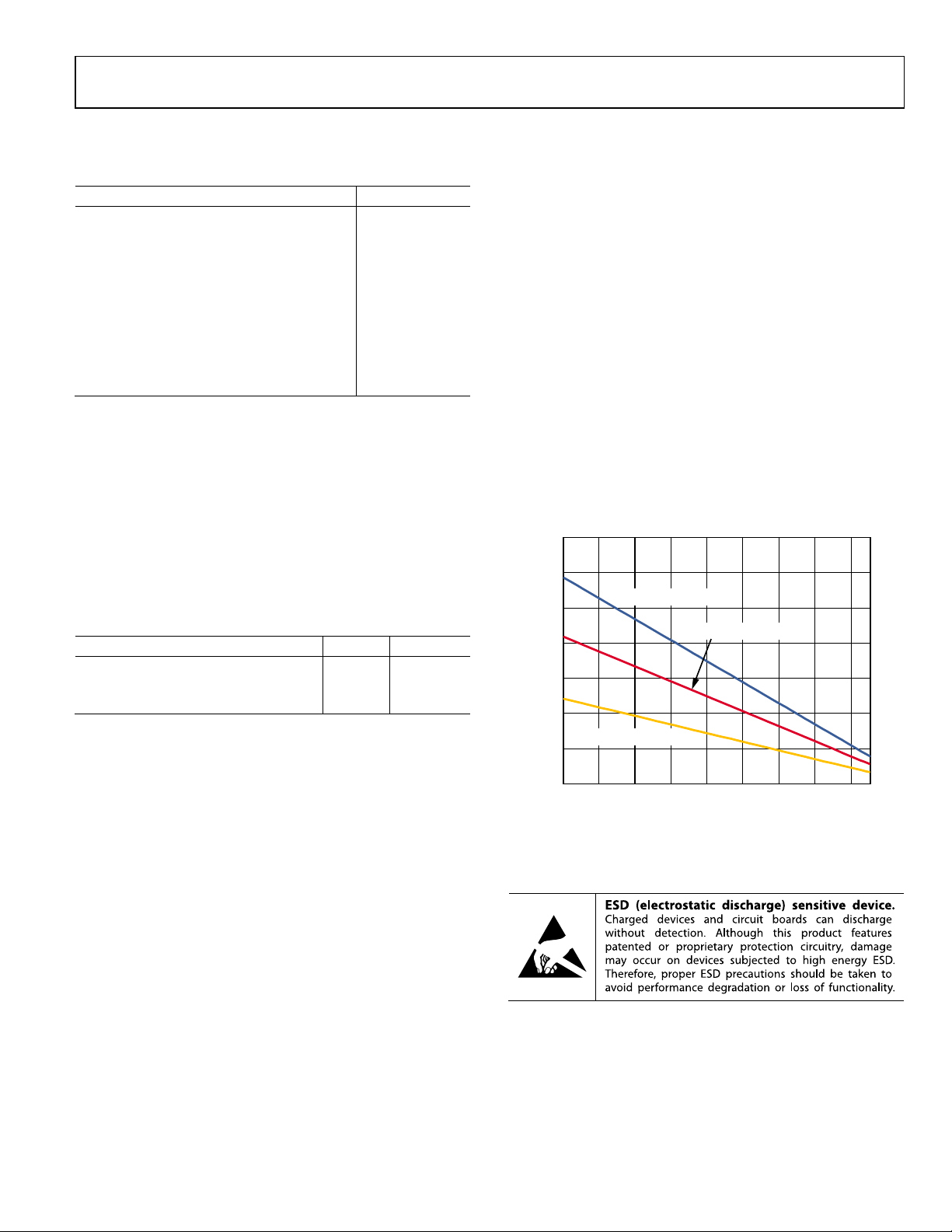
Airflow reduces θ
. In addition, more metal directly in contact
JA
with the package leads from metal traces, through holes, ground,
and power planes reduces the θ
JA
Figure 3 shows the maximum safe power dissipation in the
package vs. the ambient temperature for the 8-lead SOIC (θ
158°C/W, single)the 16-lead LFCSP (θ
24-lead LFCSP (θ
standard 4-layer board. θ
= 65.1°C /W, dual) packages on a JEDEC
JA
values are approximations.
JA
) is the sum of the
D
.
= 91.3°C/W, single) and
JA
)
S
=
JA
THERMAL RESISTANCE
θJA is specified for the worst-case conditions, that is, θJA is
specified for the device soldered on a circuit board in still air.
Table 10.
Package Type θJA Unit
8-Lead SOIC (Single)/4-Layer Board 158 °C/W
16-Lead LFCSP (Single)/4-Layer Board 91.3 °C/W
24-Lead LFCSP (Dual)/4-Layer Board 65.1 °C/W
MAXIMUM POWER DISSIPATION
The maximum safe power dissipation in the ADA4940-1/
ADA4940-2 packages is limited by the associated rise in
junction temperature (T
which is the glass transition temperature, the plastic changes its
properties. Even temporarily exceeding this temperature limit
can change the stresses that the package exerts on the die,
permanently shifting the parametric performance of the
ADA4940-1/ADA4940-2. Exceeding a junction temperature
of 150°C for an extended period can result in changes in the
silicon devices, potentially causing failure.
) on the die. At approximately 150°C,
J
Figure 3. Maximum Safe Power Dissipation vs. Ambient Temperature
ESD CAUTION
Rev. B | Page 7 of 32
ADA4940-1/ADA4940-2 Data Sheet
1–FB
2+IN
3–IN
4+FB
11 –OUT
12 DISABLE
10 +OUT
9 V
OCM
5+V
S
6+V
S
7+V
S
8+V
S
15
–V
S
16
–V
S
14
–V
S
13
–V
S
ADA4940-1
08452-101
NOTES
1. CONNECT THE EXPOSE D P AD TO
–VS OR GROUND.
08452-003
–IN
1
V
OCM
2
+V
S
3
+OUT
4
+IN
8
DISABLE
7
–V
S
6
–OUT
5
ADA4940-1
paddle (EPAD)
ground.
5
−OUT
Negative Output for Load
PIN CONFIGURATIONS AND FUNCTION DESCRIPTIONS
Figure 4. ADA4940-1 Pin Configuration (16-Lead LFCSP)
Figure 5.ADA4940-1 Pin Configuration (SOIC)
Table 11. ADA4940-1 Pin Function Descriptions (16-Lead
LFCSP)
Pin No. Mnemonic Description
1 −FB Negative Output for Feedback
Component Connection.
2 +IN Positive Input Summing Node.
3 −IN Negative Input Summing Node.
4 +FB Positive Output for Feedback
Component Connection.
5 to 8 +VS Positive Supply Voltage.
9 V
Output Common-Mode Voltage.
OCM
10 +OUT Positive Output for Load
Connection.
11 −OUT Negative Output for Load
Connection.
12
DISABLE
Disable Pin.
13 to 16 −VS Negative Supply Voltage.
Exposed
Connect the exposed pad to −VS or
Table 12. ADA4940-1 Pin Function Descriptions (8-Lead
SOIC)
Pin No. Mnemonic Description
1 −IN Negative Input Summing Node.
2 V
Output Common-Mode Voltage.
OCM
3 +VS Positive Supply Voltage.
4 +OUT Positive Output for Load
Connection.
Connection.
6 −VS Negative Supply Voltage.
7
DISABLE
Disable Pin.
8 +IN Positive Input Summing Node.
Rev. B | Page 8 of 32
Data Sheet ADA4940-1/ADA4940-2
ADA4940-2
1–IN1
2+FB1
3+V
S1
4+V
S1
5–FB2
6+IN2
15
–V
S2
16 –V
S2
17 V
OCM1
18 +OUT1
14
DISABLE2
13 –OUT2
7–IN2
8+FB2
9+V
S2
11V
OCM2
12+OUT2
10+V
S2
21
–V
S1
22
–V
S1
23
–FB1
24
+IN1
20
DISABLE1
19
–OUT1
08452-102
NOTES
1. CONNECT THE EXPOSE D P AD TO
–V
S
OR GROUND.
13
−OUT2
Negative Output 2.
Exposed paddle (EPAD)
Connect the exposed pad to −VS or ground.
Figure 6. ADA4940-2 Pin Configuration (24-Lead LFCSP)
Table 13. ADA4940-2 Pin Function Descriptions (24-Lead LFCSP)
Pin No. Mnemonic Description
1 −IN1 Negative Input Summing Node 1.
2 +FB1 Positive Output Feedback Pin 1.
3, 4 +VS1 Positive Supply Voltage 1.
5 −FB2 Negative Output Feedback Pin 2.
6 +IN2 Positive Input Summing Node 2.
7 −IN2 Negative Input Summing Node 2.
8 +FB2 Positive Output Feedback Pin 2.
9, 10 +VS2 Positive Supply Voltage 2.
11 V
Output Common-Mode Voltage 2.
OCM2
12 +OUT2 Positive Output 2.
14
DISABLE2
Disable Pin 2.
15, 16 −VS2 Negative Supply Voltage 2.
17 V
Output Common-Mode Voltage 1.
OCM1
18 +OUT1 Positive Output 1.
19 −OUT1 Negative Output 1.
20
DISABLE1
Disable Pin 1.
21, 22 −VS1 Negative Supply Voltage 1.
23 −FB1 Negative Output Feedback Pin 1.
24 +IN1 Positive Input Summing Node 1.
Rev. B | Page 9 of 32
ADA4940-1/ADA4940-2 Data Sheet
3
–9
0.1 1 10 100 1000
NORMALIZED GAIN (d B)
FREQUENCY (MHz)
08452-006
–8
–7
–6
–5
–4
–3
–2
–1
0
1
2
V
OUT, dm
= 0.1V p-p
G = 2, RL = 1kΩ
G = 2, RL = 200Ω
G = 1, RL = 200Ω
G = 1, R
L
= 1kΩ
08452-007
–9
–8
–7
–6
–5
–4
–3
–2
–1
0
1
2
3
0.1 1 10 100 1000
GAIN (dB)
FREQUENCY (MHz)
V
OUT, dm
= 0.1V p-p
V
S
= ±3.5V
VS = ±2.5V
VS = ±1.5V
3
–9
0.1 1 10 100 1000
NORMALIZED GAIN (d B)
FREQUENCY (MHz)
–8
–7
–6
–5
–4
–3
–2
–1
0
1
2
V
OUT
= 2V p-p
G = 2, R
L
= 1kΩ
G = 1, RL = 1kΩ
08452-009
G = 1, RL = 200Ω
G = 2, RL = 200Ω
08452-010
–9
–8
–7
–6
–5
–4
–3
–2
–1
0
1
2
3
0.1 1 10 100 1000
GAIN (dB)
FREQUENCY (MHz)
V
OUT
= 2V p-p
V
S
= ±3.5V
V
S
= ±2.5V
V
S
= ±1.5V
3
–9
1 10 100 1000
GAIN (dB)
FREQUENCY (MHz)
–8
–7
–6
–5
–4
–3
–2
–1
0
1
2
V
OUT, dm
= 2V p-p
08452-011
–40°C
+25°C
+125°C
3
–9
1 10 100 1000
GAIN (dB)
FREQUENCY (MHz)
–8
–7
–6
–5
–4
–3
–2
–1
0
1
2
V
OUT, dm
= 0.1V p-p
08452-008
–40°C
+25°C
+125°C
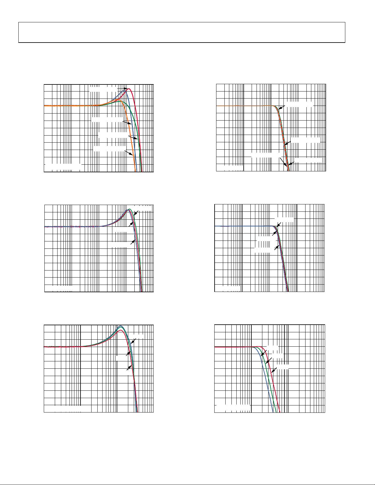
TYPICAL PERFORMANCE CHARACTERISTICS
TA = 25°C, VS = ±2.5 V, G = 1, RF = RG = 1 kΩ, RT = 52.3 Ω (when used), RL = 1 kΩ, unless otherwise noted. See Figure 59 and Figure 60 for the
test circuits.
Figure 7. Small Signal Frequency Response for Various Gains and Loads
(LFCSP)
Figure 8. Small Signal Frequency Response for Various Supplies (LFCSP)
Figure 10. Large Signal Frequency Response for Various Gains and Loads
Figure 11. Large Signal Frequency Response for Various Supplies
Figure 9. Small Signal Frequency Response for Various Temperatures (LFCSP)
Figure 12. Large Signal Frequency Response for Various Temperatures
Rev. B | Page 10 of 32

Data Sheet ADA4940-1/ADA4940-2
08452-012
4
3
–9
0.1 1 10 100 1000
GAIN (dB)
FREQUENCY (MHz)
–8
–7
–6
–5
–4
–3
–2
–1
0
1
2
V
OUT, dm
= 0.1V p-p
LFCSP-1
LFCSP-2:CH1
LFCSP-2: CH2
SOIC-1
3
–9
0.1 1 10 100 1000
GAIN (dB)
FREQUENCY (MHz)
–8
–7
–6
–5
–4
–3
–2
–1
0
1
2
V
OUT, dm
= 0.1V p-p
V
OCM
= 0V
V
OCM
= +1V
V
OCM
= –1V
08452-013
4
3
–9
0.1 1 10 100 1000
GAIN (dB)
FREQUENCY (MHz)
–8
–7
–6
–5
–4
–3
–2
–1
0
1
2
V
OUT, dm
= 0.1V p-p
08452-205
V
OCM
= –1V
V
OCM
= 0V
V
OCM
= +1V
3
–9
1 10 100 1000
GAIN (dB)
FREQUENCY (MHz)
–8
–7
–6
–5
–4
–3
–2
–1
0
1
2
V
OUT
= 2V p-p
08452-015
LFCSP-1
LFCSP-2: CH1
LFCSP-2: CH2
SOIC-1
3
–9
0.1 1 10 100 1000
GAIN (dB)
FREQUENCY (MHz)
–8
–7
–6
–5
–4
–3
–2
–1
0
1
2
V
OCM
= –1V
V
OCM
= 0V
V
OCM
= +1V
08452-016
V
OUT, dm
= 2V p-p
4
3
–9
0.1 1 10 100 1000
GAIN (dB)
FREQUENCY (MHz)
–8
–7
–6
–5
–4
–3
–2
–1
0
1
2
V
OUT, dm
= 0.1V p-p
08452-203
LFCSP: RL = 1kΩ
LFCSP: R
L
= 200Ω
SOIC: R
L
= 1kΩ
SOIC: R
L
= 200Ω
Figure 13. Small Signal Frequency Response for Various Packages
Figure 14. Small Signal Frequency Response at Various V
Levels (LFCSP)
OCM
Figure 16. Large Signal Frequency Response for Various Packages
Figure 17. Large Signal Frequency Response at Various V
OCM
Levels
Figure 15. Small Signal Frequency Response for Various V
OCM
(SOIC)
Figure 18. Small Signal Frequency Response for Various Packages and Loads
Rev. B | Page 11 of 32

ADA4940-1/ADA4940-2 Data Sheet
4
–9
1 10 100 1000
GAIN (dB)
FREQUENCY (MHz)
–8
–7
–6
–5
–4
–3
–2
–1
0
1
2
3
C
DIFF
= 0pF
V
OUT
= 0.1V p-p
C
COM1
= C
COM2
= 2pF
C
COM1
= C
COM2
= 0.5pF
C
COM1
= C
COM2
= 1pF
C
COM1
= C
COM2
= 0pF
08452-014
0.25
–0.25
0.1 10001 10 100
NORMALIZED GAIN (d B)
FREQUENCY (MHz)
–0.20
–0.15
–0.10
–0.05
0
0.05
0.10
0.15
0.20
V
OUT, dm
= 0.1V p-p
G = 2, RL = 200Ω
G = 2, RL = 1kΩ
G = 1, RL = 200Ω
G = 1, RL = 1kΩ
08452-018
3
–9
1 10 100 1000
GAIN (dB)
FREQUENCY (MHz)
–8
–7
–6
–5
–4
–3
–2
–1
0
1
2
VS = ±1.5V
VS = ±2.5V
08452-019
V
OUT, dm
= 0.1V p-p
4
–9
1 10 100 1000
GAIN (dB)
FREQUENCY (MHz)
–8
–7
–6
–5
–4
–3
–2
–1
0
1
2
3
C
COM1
= C
COM2
= 0pF
C
COM1
= C
COM2
= 0.5pF
C
COM1
= C
COM2
= 1pF
C
COM1
= C
COM2
= 2pF
C
DIFF
= 0pF
V
OUT
= 2V p-p
08452-017
0.25
–0.25
0.1 10001 10 100
NORMALIZED GAIN (d B)
FREQUENCY (MHz)
–0.20
–0.15
–0.10
–0.05
0
0.05
0.10
0.15
0.20
V
OUT, dm
= 2V p-p
G = 1, RL = 1kΩ
G = 1, RL = 200Ω
G = 2, RL = 1kΩ
G = 2, R
L
= 200Ω
08452-021
3
–9
1 10 100 1000
GAIN (dB)
FREQUENCY (MHz)
–8
–7
–6
–5
–4
–3
–2
–1
0
1
2
V
S
= ±1.5V
VS = ±2.5V
08452-022
V
OUT, dm
= 1V p-p
Figure 19. Small Signal Frequency Response for Various Capacitive Loads
(LFCSP)
Figure 20. 0.1 dB Flatness Small Signal Frequency Response for
Various Gains and Loads (LFCSP)
Figure 22. Large Signal Frequency Response for Various Capacitive Loads
Figure 23. 0.1 dB Flatness Large Signal Frequency Response for
Various Gains and Loads
Figure 21. V
OCM
Small Signal Frequency Response for Various Supplies
Figure 24. V
Large Signal Frequency Response for Various Supplies
OCM
Rev. B | Page 12 of 32

Data Sheet ADA4940-1/ADA4940-2
–20
V
= 2V p-p
OUT, dm
–30
–40
–50
HARMONIC DISTORTI ON (dBc)
–60
–70
–80
–90
–100
–110
–120
–130
0.01
0.1
HD3, G = 2
HD3, G = 1
HD2, G = 2
110
FREQUENCY ( MHz)
HD2, G = 1
08452-023
Figure 25. Harmonic Distortion vs. Frequency for Various Gains (LFCSP)
–20
V
= 2V p-p
OUT, dm
–30
–40
–50
HARMONIC DISTORTI ON (dBc)
–60
–70
–80
–90
–100
–110
–120
–130
HD2, RL = 1k
0.01
HD3, RL = 200
HD3, RL = 1k
0.1
FREQUENCY ( MHz)
HD2, RL = 200
110
08452-020
Figure 26. Harmonic Distortion vs. Frequency for Various Loads (LFCSP)
–20
V
= 2V p-p
OUT, dm
–30
–40
–50
–60
–70
–80
–90
–100
HD2, VS = ±1.5V
HARMONIC DIS TORTI ON (dBc)
HD3, VS = ±3.5V
–110
–120
–130
0.01 0.1 1 10
HD2, VS = ±3.5V
HD3, VS = ±1.5V
HD3, VS = ±2.5V
FREQUENCY ( MHz)
HD2, VS = ±2.5V
08452-024
Figure 27. Harmonic Distortion vs. Frequency for Various Supplies (LFCSP)
–20
V
= 2V p-p
OUT, dm
HARMONIC DISTORTI ON (dBc)
–30
–40
–50
–60
–70
–80
–90
–100
–110
–120
–130
0.01
HD2, G = 2
HD2, G = 1
0.1
FREQUENCY (MHz)
HD3, G = 2
HD3, G = 1
110
08452-200
Figure 28. Harmonic Distortion vs. Frequency vs. Gain (SOIC)
–20
V
= 2V p-p
OUT, dm
–30
–40
HARMONIC DIS TORTION (dBc)
–50
–60
–70
–80
–90
–100
–110
–120
–130
0.01
HD2, RL = 1k
0.1
HD3, R
HD2, R
= 200
L
= 1k
HD3, R
L
FREQUENCY (MHz)
= 200
L
110
08452-201
Figure 29. Harmonic Distortion vs. Frequency for Various Loads (SOIC)
–20
V
= 2V p-p
OUT, dm
–30
–40
–50
–60
–70
–80
–90
HARMONIC DIS TORTION (dBc)
–100
–110
–120
–130
HD2, ±1.5V
HD3, ±1.5V
0.01
HD2, ±2.5V
HD3, ±2.5V
0.1
FREQUENCY (MHz)
110
08452-202
Figure 30. Harmonic Distortion vs. Frequency for Various Supplies (SOIC)
Rev. B | Page 13 of 32

ADA4940-1/ADA4940-2 Data Sheet
–
–
–
–
–
–
20
V
= 2V p-p
OUT, dm
–30
–40
–50
–60
–70
–80
–90
–100
–110
SPURIOUS-FREE DYNAMI C RANGE (dBc)
–120
–130
0.01
SOIC: R
SOIC: R
= 200Ω
L
= 1kΩ
L
LFCSP: R
0.1
FREQUENCY (MHz)
LFCSP: RL = 1kΩ
= 200Ω
L
110
Figure 31. Spurious-Free Dynamic Range vs. Frequency at
= 200 Ω and RL = 1kΩ
R
L
20
V
= 2V p-p
OUT, dm
–30
–40
–50
–60
–70
–80
–90
–100
–110
–120
HARMONIC DIST ORTIO N (dBc)
–130
–140
–150
–2.5 2.5
HD2 AT 1MHz
–2.0 –1.5 –1.0 –0.5 0 0.5 1.0 1.5 2.0
Figure 32. Harmonic Distortion vs. V
HD3 AT 1MHz
HD2 AT 100kHz
V
(V)
OCM
HD3 AT 100kHz
for 100 kHz and 1 MHz,
OCM
±2.5 V Supplies (LFCSP)
20
–30
–40
–50
–60
–70
–80
–90
–100
HARMONIC DIST ORTION (dBc)
–110
–120
–130
0.01 0.1 1 10
HD2 AT V
HD3 AT V
OUT, dm
HD3 AT V
HD2 AT V
HD3 AT V
HD2 AT V
OUT, dm
= 2V p-p
= 8V p-p
OUT, dm
= 8V p-p
OUT, dm
= 4V p-p
OUT, dm
= 4V p-p
OUT, dm
= 2V p-p
FREQUENCY (MHz )
Figure 33. Harmonic Distortion vs. Frequency for Various V
OUT, dm
(LFCSP)
08452-030
08452-025
08452-026
20
f = 1MHz
–30
–40
–50
–60
–70
–80
VS = ±2.5V HD2
–90
–100
–110
HARMONIC DI STORT ION (d Bc)
–120
–130
–140
012345678910
Figure 34. Harmonic Distortion vs. V
VS = ±1.5V HD2
V
OUT, dm
VS = ±1.5V HD3
VS = +3V, 0V HD3
VS = +3V, 0V HD2
VS = ±3.5V HD2
VS = ±3.5V HD3
VS = ±2.5V HD3
(V p-p)
for Various Supplies, f = 1 MHz
OUT, dm
08452-027
(LFCSP)
20
+VS = +3V, –VS = 0V
–30
V
= 2V p-p
OUT, dm
–40
–50
–60
–70
–80
–90
–100
–110
HARMONIC DISTORTION (dBc)
–120
–130
–140
03.02.5
Figure 35. Harmonic Distortion vs. V
HD2 AT 1MHz
HD3 AT 1MHz
HD3 AT 100kHz
0.5 1.0 1.5 2.0
V
(V)
OCM
for 100 kHz and 1 MHz, 3 V Supply
OCM
HD2 AT 100kHz
08452-028
(LFCSP)
20
V
= 2V p-p
OUT, dm
–30
–40
–50
–60
–70
–80
–90
HD2, RF = RG = 499Ω
–100
–110
HARMONIC DISTORTI ON (dBc)
–120
–130
–140
0.01 0. 1 1 10
HD3, RF = RG = 499Ω
HD2, RF = RG = 1kΩ
FREQUENCY ( MHz)
HD3, RF = RG = 1kΩ
08452-029
Figure 36. Harmonic Distortion vs. Frequency for Various RF and RG (LFCSP)
Rev. B | Page 14 of 32

Data Sheet ADA4940-1/ADA4940-2
10
0
–120
–110
1.5 2.5
NORMALIZED SPECTRUM ( dBc)
FREQUENCY (MHz)
08452-033
–100
–90
–80
–70
–60
–50
–40
–30
–20
–10
1.6 1.7 1.8 1.9 2.0 2.1 2.2 2.42.3
V
OUT, dm
= 2V p-p
(ENVELOPE)
130
40
50
60
70
80
90
100
110
120
0.1
1
10 100
CMRR (dB)
FREQUENCY (MHz)
08452-100
SOIC
LFCSP
–10
–80
0.1
1
10 100
OUTPUT BALANCE (dB)
FREQUENCY (MHz)
–70
–60
–50
–20
–30
–40
08452-032
V
OUT, dm
= 2V p-p
–60
–130
0.1
1
10
100
CROSSTAL K ( dB)
FREQUENCY (MHz)
–120
–110
–100
–70
–80
–90
08452-039
CHANNEL 1 TO CHANNE L 2
CHANNEL 2 TO CHANNE L 1
V
OUT, dm
= 2V p-p
120
20
0.1
1
10 100
PSRR (dB)
FREQUENCY (MHz)
30
40
50
60
70
80
110
90
100
08452-034
+PSRR
–PSRR
100
–40
0
–210
10k 100k 1M 10M 100M 1G
GAIN (dB)
PHASE (Degrees)
FREQUENCY ( Hz )
08452-035
–195
–180
–165
–150
–135
–120
–105
–90
–75
–60
–45
–30
–15
–30
–20
–10
0
10
20
30
40
50
60
70
80
90
Figure 37. 2 MHz Intermodulation Distortion (LFCSP)
Figure 38. CMRR vs. Frequency
Figure 40. Crosstalk vs. Frequency, ADA4940-2
Figure 41. PSRR vs. Frequency
Figure 39. Output Balance vs. Frequency
Rev. B | Page 15 of 32
Figure 42. Open-Loop Gain and Phase vs. Frequency

ADA4940-1/ADA4940-2 Data Sheet
8
–8
–6
–4
0
2
4
6
–2
0 1000
OUTPUT VOLTAGE (V)
TIME (ns)
08452-041
100 200 300 400 500 600 700 800 900
G = +2
V
OUT, dm
2 × V
IN
100
10
1
10 100 1k 10k 100k 1M 10M
INPUT VOLTAGE NOISE (nV/√Hz)
FREQUENCY (Hz )
08452-037
1.50
–1.25
0
–2.75
0 100
OUTPUT VOLTAGE (V)
DISABLE PIN VOLTAGE (V)
TIME (µs)
08452-038
–2.50
–2.25
–2.00
–1.75
–1.50
–1.25
–1.00
–0.75
–0.50
–0.25
–1.00
–0.75
–0.50
–0.25
0
0.25
0.50
0.75
1.00
1.25
10 20 30 40 50 60 70 80 90
–OUT, V
ICM
= 1V
+OUT, V
ICM
= 1V
DISABLE
+IN
–OUT
+OUT
–F
B
+FB
–IN
V
OCM
0.1µF
R1 R2
R2
+2.5V
–2.5V
R1
V
ICM
DISABLE
0V
–2.5V
2.0
–2.0
0.5
–0.5
0 80
VOLTAGE (V)
ERROR (%)
TIME (ns)
08452-065
–0.4
–0.3
–0.2
–0.1
0
0.1
0.2
0.3
0.4
–1.6
–1.2
–0.8
–0.4
0
0.4
0.8
1.2
1.6
10 20 30 40 50 60 70
%ERROR
OUTPUT
INPUT
V
OUT, dm
= 2V p-p
100
10
1
0.1
0.01
0.1 1 10 100
OUTPUT IMPEDANCE (Ω)
FREQUENCY (MHz)
08452-040
2.50
–0.25 –2.75
0 2.0
OUTPUT VOLTAGE (V)
DISABLE PIN VOLTAGE (V)
TIME (µs)
08452-057
–2.50
–2.25
–2.00
–1.75
–1.50
–1.25
–1.00
–0.75
–0.50
–0.25
0
0
0.25
0.50
0.75
1.00
1.25
1.50
1.75
2.00
2.25
0.2 0.4 0.6 0.8 1.0 1.2 1.4 1.6 1.8
–OUT, V
ICM
= 1V
DISABLE
+OUT, V
ICM
= 1V
+IN
–OUT
+OUT
–FB
+FB
–IN
V
OCM
0.1µF
R1 R2
R2
+2.5V
–2.5V
R1
V
ICM
DISABLE
0V
–2.5V
Figure 43. Output Overdrive Recovery, G = 2
Figure 44. Voltage Noise Spectral Density, Referred to Input
Figure 46. 0.1% Settling Time
Figure 47. Closed-Loop Output Impedance Magnitude vs. Frequency, G = 1
Figure 45.
DISABLE
Pin Turn-Off Time
Figure 48.
DISABLE
Pin Turn-On Time
Rev. B | Page 16 of 32

Data Sheet ADA4940-1/ADA4940-2
100
–100
0 150
OUTPUT VOLTAGE (mV)
TIME (ns)
–80
–60
–40
–20
0
20
40
60
80
10 20 30 40 50 60 70 80 90 100 110 120 130 140
V
OUT, dm
= 0.1V p-p
G = 2, RL = 1kΩ
G = 1, R
L
= 1kΩ
G = 1, RL = 200Ω
G = 2, R
L
= 200Ω
08452-042
–100
–80
–60
–40
–20
0
20
40
60
80
100
0 10 20 30 40 50 60 70 80 90 100 110 120 130 140 150
OUTPUT VOLTAGE (mV)
TIME (ns)
V
OUT, dm
= 0.1V
VS = ±1.5V
VS = ±3.5V
VS = ±2.5V
08452-043
100
–100
0 150
OUTPUT VOLTAGE (mV)
TIME (ns)
–80
–60
–40
–20
0
20
40
60
80
10 20 30 40 50 60 70 80 90 100 110 120 130 140
C
DIFF
= 0pF
V
OUT, dm
= 0.1V p-p
C
COM1
= C
COM2
= 0pF
C
COM1
= C
COM2
= 0.5pF
C
COM1
= C
COM2
= 1pF
C
COM1
= C
COM2
= 2pF
08452-044
1.5
1.0
0.5
0
–0.5
–1.0
–1.5
OUTPUT VOLTAGE (V)
TIME (ns)
V
OUT, dm
= 2V p-p
G = 1, RL = 1kΩ
G = 1, R
L
= 200Ω
G = 2, R
L
= 1kΩ
G = 2, R
L
= 200Ω
08452-045
0 30020 40 60 80 100 120 140 160 180 200 220 240 260 280
–1.5
–1.0
–0.5
0
0.5
1.0
1.5
0 20 40 60 80 100 120 140 160 180 200 220 240 260 280 300
OUTPUT VOLTAGE (V)
TIME (ns)
V
OUT, dm
= 2V p-p
V
S
= ±3.5V
V
S
= ±1.5V
VS = ±2.5V
08452-046
1.5
1.0
0.5
0
–0.5
–1.0
–1.5
OUTPUT VOLTAGE (V)
TIME (ns)
C
DIFF
= 0pF
V
OUT, dm
= 2V p-p
C
COM1
= C
COM2
= 0pF
C
COM1
= C
COM2
= 0.5pF
C
COM1
= C
COM2
= 1pF
C
COM1
= C
COM2
= 2pF
08452-047
0 30020 40 60 80 100 120 140 160 180 200 220 240 260 280
Figure 49. Small Signal Transient Response for Various Gains and Loads
(LFCSP)
Figure 50. Small Signal Transient Response for Various Supplies (LFCSP)
Figure 52. Large Signal Transient Response for Various Gains and Loads
Figure 53. Large Signal Transient Response for Various Supplies
(LFCSP)
Figure 51. Small Signal Transient Response for Various Capacitive Loads
Figure 54. Large Signal Transient Response for Various Capacitive Loads
Rev. B | Page 17 of 32

ADA4940-1/ADA4940-2 Data Sheet
100
–100
–80
–60
–40
–20
0
20
40
60
80
0 10 20 30 40 50 60 70 80 90 100 110 120 130 140 150
OUTPUT VOLTAGE (mV)
TIME (ns)
V
OUT, dm
= 0.1V p-p
08452-204
LFCSP-1
LFCSP-2: CH1
LFCSP-2: CH2
SOIC-1
100
–100
0 150
OUTPUT VOLTAGE (mV)
TIME (ns)
–80
–60
–40
–20
0
20
40
60
80
10 20 30 40 50 60 70 80 90 100 110 120 130 140
V
OUT, dm
= 0.1V p-p
V
S
= ±1.5V
VS = ±2.5V
08452-048
100
–100
–80
–60
–40
–20
0
20
40
60
80
0 10 20 30 40 50 60 70 80 90 100 110 120 130 140 150
OUTPUT VOLTAGE (mV)
TIME (ns)
V
OUT, dm
= 0.1V p-p
08452-206
LFCSP-1
LFCSP-2: CH1
LFCSP-2: CH2
SOIC-1
1.00
–1.00
0 300
OUTPUT VOLTAGE (V)
TIME (ns)
–0.75
–0.50
–0.25
0
0.25
0.50
0.75
20 40 60 80 100 120 140 160 180 200 220 240 260 280
V
OUT, dm
= 1V p-p
V
S
= ±1.5V
VS = ±2.5V
08452-053
Figure 55. Small Signal Transient Response for Various Packages, CL = 0 pF
Figure 56. V
Small Signal Transient Response
OCM
Figure 57. Small Signal Transient Response for Various Packages, CL = 2 pF
Figure 58. V
Large Signal Transient Response
OCM
Rev. B | Page 18 of 32

Data Sheet ADA4940-1/ADA4940-2
ADA4940-1/
ADA4940-2
54.9Ω
475Ω
475Ω
54.9Ω
+2.5V
–2.5V
1kΩ
1kΩ
50Ω
NETWORK
ANALYZER
OUTPUT
NETWORK
ANALYZER
INPUT
1kΩ
1kΩ
V
OCM
52.3Ω
25.5Ω
V
IN
08452-067
50Ω
50Ω
ADA4940-1/
ADA4940-2
+2.5V
–2.5V
1kΩ
1kΩ
50Ω
1kΩ
475Ω
475Ω
1kΩ
V
OCM
52.3Ω
54.9Ω
54.9Ω
100Ω
HP
LP
2:1
50Ω
CT
V
IN
LOW-PASS
FILTER
DC-COUPLED
GENERATOR
DUAL
FILTER
08452-056
25.5Ω
TEST CIRCUITS
Figure 59. Equivalent Basic Test Circuit
Figure 60. Test Circuit for Distortion Measurements
Rev. B | Page 19 of 32

ADA4940-1/ADA4940-2 Data Sheet
ADA4840-1/
ADA4940-2
R
L, dm
V
OUT, dm
R
F
R
F
R
G
R
G
+FB
+IN
+OUT
–OUT
–
+
+D
IN
+V
OCM
–D
IN
–FB
–IN
08452-090
dmOS,
cmIN,
DIFF
ΔV
ΔV
CMRR =
dmOS,
OCM
V
ΔV
ΔV
CMRR
OCM
=
dmOUT
cmOUT
V
V
ErrorBalanceOutput
,
,
=
TERMINOLOGY
DEFINITION OF TERMS
Figure 61. Circuit Definitions
Differential Voltage
Differential voltage refers to the difference between two node
voltages. For example, the differential output voltage (or
equivalently, output differential mode voltage) is defined as
V
= (V
OUT, dm
where V
+OUT
and V
−OUT terminals with respect to a common reference.
Similarly, the differential input voltage is defined as
V
= (+DIN − (−DIN))
IN, dm
Common-Mode Voltage (CMV)
CMV refers to the average of two node voltages. The output
common-mode voltage is defined as
V
= (V
OUT, cm
Similarly, the input common-mode voltage is defined as
V
= (+DIN + (−DIN))/2
IN, cm
+OUT
+OUT
− V
−OUT
+ V
)
−OUT
refer to the voltages at the +OUT and
)/2
−OUT
Common-Mode Offset Voltage
The common-mode offset voltage is defined as the difference
between the voltage applied to the V
terminal and the
OCM
common mode of the output voltage.
V
= V
OS, cm
Differential VOS, Differential CMRR, and V
OUT, cm
− V
OCM
CMRR
OCM
The differential mode and common-mode voltages each have
their own error sources. The differential offset (V
OS, dm
) is the
voltage error between the +IN and −IN terminals of the amplifier.
Differential CMRR reflects the change of V
in response to
OS, dm
changes to the common-mode voltage at the input terminals
+D
and −DIN.
IN
V
CMRR reflects the change of V
OCM
in response to
OS, dm
changes to the common-mode voltage at the output terminals.
Balance
Balance is a measure of how well the differential signals are
matched in amplitude; the differential signals are exactly 180°
apart in phase. By this definition, the output balance is the
magnitude of the output common-mode voltage divided by
the magnitude of the output differential mode voltage.
Rev. B | Page 20 of 32

Data Sheet ADA4940-1/ADA4940-2
08452-058
G
O
C
C
C
C
R
F
R
G
G
CM
G
DIFF
G
O
R
G
V
REF
–OUT
+OUT
R
F
+D
IN
–D
IN
+IN
–IN
V
OCM
F
OUT
G
IN
R
V
R
D
−
−=
+
F
OUT
G
IN
R
V
R
D
+
−=
−
G
F
R
R
2
dmOUT,
V
2
dmOUT,
V
+
+
+
+=
−
+
G
F
G
OUT
G
F
F
ININ
RR
R
V
RR
R
DV
+
+
+
−=
+
−
G
F
G
OUT
G
F
F
ININ
RR
R
V
RR
R
DV
THEORY OF OPERATION
The ADA4940-1/ADA4940-2 are high speed, low power
differential amplifiers fabricated on Analog Devices advanced
dielectrically isolated SiGe bipolar process. They provide two
closely balanced differential outputs in response to either
differential or single-ended input signals. An external feedback
network that is similar to a voltage feedback operational
amplifier sets the differential gain. The output common-mode
voltage is independent of the input common-mode voltage and
is set by an external voltage at the V
terminal. The PNP
OCM
input stage allows input common-mode voltages between the
negative supply and 1.2 V below the positive supply. A rail-to-
rail output stage supplies a wide output voltage range.
DISABLE
The
pin can be used to reduce the supply current of
the amplifier to 13.5 µA.
Figure 62 shows the ADA4940-1/ADA4940-2 architecture.
The differential feedback loop consists of the differential trans-
conductance G
the R
feedback networks. The common-mode feedback
F/RG
working through the GO output buffers and
DIFF
loop is set up with a voltage divider across the two differential
outputs to create an output voltage midpoint and a common-
mode transconductance, G
CM
.
The differential feedback loop forces the voltages at +IN and −IN
to equal each other. This fact sets the following relationships:
Subtracting the previous equations gives the relationship that
shows RF and RG setting the differential gain.
(V
+OUT
− V
) = (+DIN – (−DIN)) ×
−OUT
The common-mode feedback loop drives the output commonmode voltage that is sampled at the midpoint of the output
voltage divider to equal the voltage at V
. This results in the
OCM
following relationships:
V
= V
V
+OUT
−OUT
= V
OCM
OCM
+
−
Note that the differential amplifier’s summing junction input
voltages, +IN and −IN, are set by both the output voltages and
the input voltages.
Figure 62. ADA4940-1/ADA4940-2 Architectural Block
Rev. B | Page 21 of 32

ADA4940-1/ADA4940-2 Data Sheet
G
F
dmIN
dmOUT
R
R
V
V
=
,
,
ADA4940-1/
ADA4940-2
+
R
F2
V
nOD
V
nCM
V
OCM
V
nIN
R
F1
R
G2
R
G1
V
nRF1
V
nRF2
V
nRG1
V
nRG2
i
nIN+
i
nIN–
08452-050
( )
21
N
ββG+
=
2
G1
F1
G1
1
RR
R
β+=
G2
F2
G2
2
RR
R
β+=
G
F
N
R
R
β
G +== 1
1
∑
=
=
8
1i
2
nOinOD
vv
APPLICATIONS INFORMATION
ANALYZING AN APPLICATION CIRCUIT
The ADA4940-1/ADA4940-2 use open-loop gain and negative
feedback to force their differential and common-mode output
voltages in such a way as to minimize the differential and commonmode error voltages. The differential error voltage is defined as
the voltage between the differential inputs labeled +IN and −IN (see
Figure 61). For most purposes, this voltage can be assumed to be
zero. Similarly, the difference between the actual output commonmode voltage and the voltage applied to V
to be zero. Starting from these two assumptions, any application
circuit can be analyzed.
SETTING THE CLOSED-LOOP GAIN
The differential mode gain of the circuit in Figure 61 can be
determined by
can also be assumed
OCM
Figure 63. ADA4940-1/ADA4940-2 Noise Model
As with conventional op amp, the output noise voltage densities
can be estimated by multiplying the input-referred terms at +IN
and −IN by the appropriate output factor,
where:
is the circuit noise gain.
This assumes that the input resistors (R
(R
) on each side are equal.
F
) and feedback resistors
G
ESTIMATING THE OUTPUT NOISE VOLTAGE
The differential output noise of the ADA4940-1/ADA4940-2 can
be estimated using the noise model in Figure 63. The input-referred
noise voltage density, v
the noise currents, i
ground. The noise currents are assumed to be equal and produce
a voltage across the parallel combination of the gain and feedback
resistances. v
is the noise voltage density at the V
nCM
of the four resistors contributes (4kTR
the input noise sources, the multiplication factors, and the
output-referred noise density terms. For more noise calculation
information, go to the Analog Devices Differential Amplifier
Calculator (DiffAmpCalc™), click ADIDiffAmpCalculator.zip
and follow the on-screen prompts.
Table 14. Output Noise Voltage Density Calculations
Input Noise Contribution Input Noise Term
Differential Input v
Inverting Input i
Noninverting Input i
V
Input v
OCM
Gain Resistor RG1 v
Gain Resistor RG2 v
Feedback Resistor RF1 v
Feedback Resistor RF2 v
, is modeled as a differential input, and
nIN
nIN−
and i
, appear between each input and
nIN+
1/2
)
. Table 14 summarizes
x
v
nIN
i
nIN−
i
nIN+
v
nCM
(4kTRG1)
nRG1
(4kTRG2)
nRG2
(4kTRF1)
nRF1
(4kTRF2)
nRF2
pin. Each
OCM
Input Noise
Voltage Density
and
When R
= RF2/RG2, then β1 = β2 = β, and the noise gain
F1/RG1
becomes
Note that the output noise from V
The total differential output noise density, v
square of the individual output noise terms.
Output
Multiplication Factor
GN v
nIN
× (RG2||RF2) GN v
nIN−
× (RG1||RF1) GN v
nIN+
GN (β1 − β2) v
nCM
1/2
GN (1 − β2) v
1/2
GN (1 − β1) v
1/2
1 v
1/2
1 v
are the feedback factors.
goes to zero in this case.
OCM
, is the root-sum-
nOD
Output-Referred Noise
Voltage Density Term
= GN (v
nO1
= GN [i
nO2
= GN [i
nO3
= GN (β1 − β2)(v
nO4
= GN (1 − β2)(4kTRG1)
nO5
= GN (1 − β1)(4kTRG2)
nO6
= (4kTRF1)
nO7
= (4kTRF2)
nO8
)
nIN
× (RG2||RF2)]
nIN−
× (RG1||RF1)]
nIN+
1/2
1/2
nCM
)
1/2
1/2
Rev. B | Page 22 of 32

Data Sheet ADA4940-1/ADA4940-2
6
1000
500
1000
15.4
7.7
10
1000
318
636
20.0
6.8
14
1000
196
392
27.7
5.5
Nominal Gain (dB)
RF (Ω)
RG (Ω)
(Ω)
R
(Ω)
RG1 (Ω)1
Differential Output Noise Density (nV/√Hz)
RTI (nV/√Hz)
0
1000
1000
52.3
1333
1025
11.2
11.2
6
1000
500
53.6
750
526
15.0
7.5
10
1000
318
54.9
512
344
19.0
6.3
14
1000
196
59.0
337
223
25.3
5
( )
+×
−
=
FG
F
G
seIN
RR
R
R
R
2
1
,
+V
S
ADA4940-1/
ADA4940-2
+IN
–IN
R
F
R
F
+D
IN
–D
IN
V
OCM
R
G
R
G
V
OUT, dm
08452-051
R
T
R
S
ADA4940-1/
ADA4940-2
+V
S
R
F
R
G
R
S
R
G
R
F
V
OCM
R
T
V
OUT, dm
08452-052
+IN
–IN
Table 15 and Table 16 list several common gain settings, recommended resistor values, input impedances, and output noise density for both
balanced and unbalanced input configurations.
Table 15. Differential Ground-Referenced Input, DC-Coupled, R
Nominal Gain (dB) RF (Ω) RG (Ω) R
(Ω) Differential Output Noise Density (nV/√Hz) RTI (nV/√Hz)
IN, dm
0 1000 1000 2000 11.3 11.3
Table 16. Single-Ended Ground-Referenced Input, DC-Coupled, RS = 50 Ω, RL = 1 kΩ (See Figure 65)
1
RG1 = RG + (RS||RT)
RT
IN, se
IMPACT OF MISMATCHES IN THE FEEDBACK
NETWORKS
Even if the external feedback networks (RF/RG) are mismatched,
the internal common-mode feedback loop still forces the outputs
to remain balanced. The amplitudes of the signals at each output
remain equal and 180° out of phase. The input-to-output,
differential mode gain varies proportionately to the feedback
mismatch, but the output balance is unaffected.
As well as causing a noise contribution from V
, ratio-matching
OCM
errors in the external resistors result in a degradation of the ability
of the circuit to reject input common-mode signals, much the
same as for a four resistors difference amplifier made from a
conventional op amp.
In addition, if the dc levels of the input and output common-
mode voltages are different, matching errors result in a small
differential mode, output offset voltage. When G = 1, with a
ground-referenced input signal and the output common-mode
level set to 2.5 V, an output offset of as much as 25 mV (1% of
the difference in common-mode levels) can result if 1% tolerance
resistors are used. Resistors of 1% tolerance result in a worst-
case input CMRR of about 40 dB, a worst-case differential mode
output offset of 25 mV due to the 2.5 V level-shift, and no
significant degradation in output balance error.
CALCULATING THE INPUT IMPEDANCE OF AN
APPLICATION CIRCUIT
The effective input impedance of a circuit depends on whether
the amplifier is being driven by a single-ended or differential
signal source. For balanced differential input signals, as shown
in Figure 64, the input impedance (R
(+D
and −DIN) is simply R
IN
IN, dm
= 2 × RG.
) between the inputs
IN, dm
= 1 kΩ (See Figure 64)
L
For an unbalanced, single-ended input signal (see Figure 65),
the input impedance is
Figure 64. ADA4940-1/ADA4940-2 Configured for Ba lanced (Differentia l) Inputs
Figure 65. ADA4940-1/ADA4940-2 Configured for Unbalan ced (Single-Ended) In put
The input impedance of the circuit is effectively higher than it
would be for a conventional op amp connected as an inverter
because a fraction of the differential output voltage appears at
the inputs as a common-mode signal, partially bootstrapping
the voltage across the input resistor R
G1.
Rev. B | Page 23 of 32

R
S
50Ω
V
S
2V p-p
R
IN, se
1.33kΩ
ADA4940-1
ADA4940-2
RLV
OUT, dm
+V
S
–V
S
R
G
1kΩ
R
G
1kΩ
R
F
1kΩ
R
F
1kΩ
V
OCM
08452-059
Ωk.331
)10001000(2
1000
1
1000
)(2
1
,
=
+×
−
=
+×
−
=
F
G
F
G
seIN
RR
R
R
R
ADA4940-1
ADA4940-2
RLV
OUT, dm
+V
S
–V
S
R
S
50Ω
R
G
1kΩ
R
G
1kΩ
R
F
1kΩ
R
F
1kΩ
V
OCM
V
S
2V p-p
R
IN, se
50Ω
R
T
52.3Ω
08452-060
R
S
50Ω
V
S
2V p-p
R
T
52.3Ω
R
TH
25.5Ω
V
TH
1.02V p-p
08452-061
ADA4940-1
ADA4940-2
R
L
V
OUT, dm
+V
S
–V
S
R
TH
25.5Ω
R
G
1kΩ
R
G
1kΩ
R
F
1kΩ
R
F
1kΩ
V
OCM
V
TH
1.02V p-p
R
TS
25.5Ω
08452-062
ADA4940-1/ADA4940-2 Data Sheet
Terminating a Single-Ended Input
This section describes how to properly terminate a single-ended
input to the ADA4940-1/ADA4940-2 with a gain of 1, R
and R
= 1 kΩ. An example using an input source with a terminated
G
output voltage of 1 V p-p and source resistance of 50 Ω illustrates
the three steps that must be followed. Because the terminated
output voltage of the source is 1 V p-p, the open-circuit output
voltage of the source is 2 V p-p. The source shown in Figure 66
indicates this open-circuit voltage.
Figure 66. Calculating Single-Ended Input Impedance, R
1. The input impedance is calculated by
2. To match the 50 Ω source resistance, calculate the
termination resistor, R
The closest standard 1% value for R
Figure 67. Adding Termination Resistor R
, using RT||1.33 kΩ = 50 Ω.
T
is 52.3 Ω.
T
3. Figure 67 shows that the effective RG in the upper feedback
loop is now greater than the R
in the lower loop due to the
G
addition of the termination resistors. To compensate for the
imbalance of the gain resistors, add a correction resistor (R
in series with R
equivalent of the source resistance, R
resistance, R
in the lower loop. RTS is the Thevenin
G
, and is equal to RS||RT.
T
, and the termination
S
T
= 1 kΩ
F
IN
)
TS
Rev. B | Page 24 of 32
Figure 68. Calculating the Thevenin Equivalent
RTS = RTH = RS||RT = 25.5 Ω. Note that VTH is greater than
1 V p-p, which was obtained with R
= 50 Ω. The modified
T
circuit with the Thevenin equivalent (closest 1% value used for
R
) of the terminated source and RTS in the lower feedback
TH
loop is shown in Figure 69.
Figure 69. Thevenin Equivalent and Matched Gain Resistors
Figure 69 presents a tractable circuit with matched feedback
loops that can be easily evaluated.
It is useful to point out two effects that occur with a terminated
input. The first is that the value of R
is increased in both loops,
G
lowering the overall closed-loop gain. The second is that V
is a little larger than 1 V p-p, as it would be if R
These two effects have opposite impacts on the output voltage,
and for large resistor values in the feedback loops (~1 kΩ), the
effects essentially cancel each other out. For small R
or high gains, however, the diminished closed-loop gain is not
cancelled completely by the increased V
. This can be seen by
TH
evaluating Figure 69.
The desired differential output in this example is 1 V p-p
because the terminated input signal was 1 V p-p and the
closed-loop gain = 1. The actual differential output voltage,
however, is equal to (1.02 V p-p)(1000/1025.5) = 0.996 V p-p.
This is within the tolerance of the resistors, so no change to
the feedback resistor, R
, is required.
F
INPUT COMMON-MODE VOLTAGE RANGE
The ADA4940-1/ADA4940-2 input common-mode range is
shifted down by approximately 1 V
drivers with centered input ranges, such as the ADA4939-x. The
downward-shifted input common-mode range is especially
suited to dc-coupled, single-ended-to-differential, and singlesupply applications.
For ±2.5 V or +5 V supply operation, the input common-mode
range at the summing nodes of the amplifier is specified as −2.7 V
to +1.3 V or −0.2 V to 3.8 V, and is specified as −0.2 V to +1.8 V
with a +3 V supply.
, in contrast to other ADC
BE
= 50 Ω.
T
and RG,
F
TH

08452-063
DISABLE
AMPLIFIER
BIAS CURRENT
–V
S
+V
S
120
0
5 10010 1000
08452-064
20
40
60
80
100
SERIES RESISTANCE (Ω)
LOAD CAPACITANCE (pF)
+IN
–OUT
+OUT
–FB
+FB
–IN
V
OCM
0.1µF
R
S
R
S
R1
C
L
C
L
R2
R4
+2.5V
–2.5V
R3
V
IN
Data Sheet ADA4940-1/ADA4940-2
INPUT AND OUTPUT CAPACITIVE AC COUPLING
Although the ADA4940-1/ADA4940-2 is best suited to dccoupled applications, it is nonetheless possible to use it in accoupled circuits. Input ac coupling capacitors can be inserted
between the source and R
of the dc common-mode feedback current and causes the
ADA4940-1/ADA4940-2 dc input common-mode voltage to
equal the dc output common-mode voltage. These ac coupling
capacitors must be placed in both loops to keep the feedback
factors matched. Output ac coupling capacitors can be placed in
series between each output and its respective load.
SETTING THE OUTPUT COMMON-MODE VOLTAGE
The V
biased at a voltage approximately equal to the midsupply point,
[(+V
output common-mode voltage that is within approximately
100 mV of the expected value.
In cases where more accurate control of the output common-mode
level is required, it is recommended that an external source, or
resistor divider (10 kΩ or greater resistors), be used. The output
common-mode offset listed in the Specifications section assumes
that the V
It is also possible to connect the V
level (CML) output of an ADC. However, care must be taken to
ensure that the output has sufficient drive capability. The input
impedance of the V
DISABLE
The ADA4940-1/ADA4940-2 feature a
be used to minimize the quiescent current consumed when the
device is not being used.
logic level to the
low logic levels is nominally 1.4 V above the negative supply rail.
See Tabl e 5 and Table 8 for the threshold limits.
The
enables the amplifier for normal operation. The ADA4940-1/
ADA4940-2
external connection is required) and does not require an
external pull-up resistor to ensure normal on operation (see
Figure 70). When the ADA4940-1/ADA4940-2 is disabled, the
output is high impedance. Note that the outputs are tied to the
inputs through the feedback resistors and to the source using the
gain resistors. In addition, there are back-to-back diodes on the
input pins that limit the differential voltage to 1.2 V.
pin of the ADA4940-1/ADA4940-2 is internally
OCM
) + (−VS)]/2. Relying on this internal bias results in an
S
input is driven by a low impedance voltage source.
OCM
PIN
DISABLE
DISABLE
pin features an internal pull-up network that
DISABLE
. This ac coupling blocks the flow
G
input to a common-mode
OCM
pin is approximately 250 kΩ.
OCM
DISABLE
DISABLE
is asserted by applying a low
pin that can
pin. The threshold between high and
pin can be left floating (that is, no
DISABLE
Figure 70.
Pin Circuit
DRIVING A CAPACITIVE LOAD
A purely capacitive load reacts with the bond wire and pin
inductance of the ADA4940-1/ADA4940-2, resulting in high
frequency ringing in the transient response and loss of phase
margin. One way to minimize this effect is to place a resistor in
series with each output to buffer the load capacitance. The resistor
and load capacitance form a first-order, low-pass filter; therefore,
the resistor value should be as small as possible. In some cases,
the ADCs require small series resistors to be added on their inputs.
Figure 71 illustrates the capacitive load vs. the series resistance
required to maintain a minimum 45° of phase margin.
Figure 71. Capacitive Load vs. Series Resistance (LFSCP)
Rev. B | Page 25 of 32

ADA4940-1/ADA4940-2 Data Sheet
0
–160
–140
–120
–100
–80
–60
–40
–20
0 20k 40k 60k 80k 100k
AMPLIT UDE ( dB)
FREQUENCY ( Hz )
08452-069
08452-066
33Ω
33Ω
10µF
R1
–D
IN
+2.5V
+5V
+6V
–1V
R2
R4
+6V
REF
VDD
GND
IN+
IN–
AD7982
2.7nF
2.7nF
–IN
+OUT
–OUT
+IN
R3
+D
IN
ADR435
0.1µFR6
R5
SERIAL
INTERFACE
–FB
+FB
ADA4940-1
V
OCM
DRIVING A HIGH PRECISION ADC
The ADA4940-1/ADA4940-2 are ideally suited for broadband
dc-coupled applications. The circuit in Figure 73 shows a frontend connection for an ADA4940-1 driving an AD7982, which is
an 18-bit, 1 MSPS successive approximation, analog-to-digital
converter (ADC) that operates from a single power supply, 3 V
to 5 V. It contains a low power, high speed, 18-bit sampling
ADC and a versatile serial interface port. The reference voltage,
REF, is applied externally and can be set independent of the
supply voltage. As shown in Figure 73, the ADA4940-1 is dccoupled on the input and the output, which eliminates the need
for a transformer to drive the ADC. The amplifier performs a
single-ended-to-differential conversion if needed and level
shifts the input signal to match the input common mode of the
ADC. The ADA4940-1 is configured with a dual 7 V supply
(+6 V and −1 V) and a gain that is set by the ratio of the
feedback resistor to the gain resistor. In addition, the circuit
can be used in a single-ended-input-to-differential output or
differential-input-to-differential output configuration. If needed,
a termination resistor in parallel with the source input can be
used. Whether the input is a single-ended input or differential,
the input impedance of the amplifier can be calculated as shown in
the Terminating a Single-Ended Input section. If R1 = R2 = R3 =
R4 = 1 kΩ, the single-ended input impedance is approximately
1.33 kΩ, which, in parallel with a 52.3 Ω termination resistor,
provides a 50 Ω termination for the source. An additional 25.5 Ω
(1025.5 Ω total) at the inverting input balances the parallel
impedance of the 50 Ω source and the termination resistor driving
the noninverting input. However, if a differential source input is
used, the differential input impedance is 2 kΩ. In this case, two
52.3 Ω termination resistors are used to terminate the inputs.
In this example, the signal generator has a 10 V p-p symmetric,
ground-referenced bipolar output. The V
noise reduction and set externally with 1% resistors to 2.5 V to
maximize the output dynamic range. With an output common-
input is bypassed for
OCM
mode voltage of 2.5 V, each ADA4940-1 output swings between 0
V and 5 V, opposite in phase, providing a gain of 1 and a 10 V pp differential signal to the ADC input. The differential RC section
between the ADA4940-1 output and the ADC provides single-pole,
low-pass filtering with a corner frequency of 1.79 MHz and extra
buffering for the current spikes that are output from the ADC input
when its sample-and-hold (SHA) capacitors are discharged.
The total system power in Figure 73 is under 35 mW. A large
portion of that power is the current coming from supplies to the
output, which is set at 2.5 V, going back to the input through the
feedback and gain resistors. To reduce that power to 25 mW,
increase the value of the feedback and gain resistor from 1 kΩ
to 2 kΩ and set the value of the resistors R5 and R6 to 3 kΩ. The
ADR435 is used to regulate the +6 V supply to +5 V, which ends
up powering the ADC and setting the reference voltage for the
V
pin.
OCM
Figure 72 shows the fft of a 20 kHz differential input tone
sampled at 1 MSPS. The second and third harmonics are down
at −118 dBc and −122 dBc.
Figure 72. Distortion Measurement of a 20 kHz Input Tone (CN-0237)
Figure 73. ADA4940-1 (LFCSP) Driving the AD7982 ADC
Rev. B | Page 26 of 32

Data Sheet ADA4940-1/ADA4940-2
08452-086
1.30
0.80
0.80
1.30
08452-087
0.30
PLATED
VIA HOLE
1.30
GROUND PLANE
POWER PLANE
BOTTOM METAL
TOP METAL
08452-088
LAYOUT, GROUNDING, AND BYPASSING
As a high speed device, the ADA4940-1/ADA4940-2 are
sensitive to the PCB environment in which they operate.
Realizing their superior performance requires attention to
the details of high speed PCB design.
ADA4940-1 LFCSP EXAMPLE
The first requirement is a solid ground plane that covers as
much of the board area around the ADA4940-1 as possible.
However, clear the area near the feedback resistors (R
resistors (R
), and the input summing nodes (Pin 2 and Pin 3)
G
of all ground and power planes (see Figure 74). Clearing the
ground and power planes minimizes any stray capacitance at
these nodes and prevents peaking of the response of the
amplifier at high frequencies.
The thermal resistance, θ
, is specified for the device, including
JA
the exposed pad, soldered to a high thermal conductivity 4-layer
circuit board, as described in EIA/JESD 51-7.
), gain
F
Bypass the power supply pins as close to the device as possible
and directly to a nearby ground plane. Use high frequency ceramic
chip capacitors. Use two parallel bypass capacitors (1000 pF and
0.1 µF) for each supply. Place the 1000 pF capacitor closer to the
device. Further away, provide low frequency bypassing using
10 µF tantalum capacitors from each supply to ground.
Ensure that signal routing is short and direct to avoid parasitic
effects. Wherever complementary signals exist, provide a
symmetrical layout to maximize balanced performance. When
routing differential signals over a long distance, ensure that
PCB traces are close together, and twist any differential wiring
such that loop area is minimized. Doing this reduces radiated
energy and makes the circuit less susceptible to interference.
Figure 74. Ground and Power Plane Voiding in Vicinity of R
Figure 76. Cross-Section of 4-Layer PCB Showing Thermal Via Connection to Buried Ground Plane (Dimensions in mm)
and RG
F
Figure 75. Recommended PCB Thermal Attach Pad Dimensions (mm)
Rev. B | Page 27 of 32

ADA4940-1/ADA4940-2 Data Sheet
1
0.50
BSC
0.60 MAX
PIN 1
INDICATOR
1.50 REF
0.50
0.40
0.30
0.25 MIN
0.45
2.75
BSC SQ
TOP
VIEW
12° MAX
0.80 MAX
0.65 TYP
SEATING
PLANE
PIN 1
INDICATOR
1.00
0.85
0.80
0.30
0.23
0.18
0.05 MAX
0.02 NOM
0.20 REF
3.00
BSC SQ
*
1.45
1.30 SQ
1.15
EXPOSED
PAD
16
5
13
8
9
12
4
(BOTTOM VIEW)
*
COMPLIANT
TO
JEDEC STANDARDS MO-220-VEED-2
EXCEPT FOR EXPOSED PAD DIMENSION.
072208-A
FOR PROP E R CONNECTION OF
THE EXPOSED PAD, REFER TO
THE PIN CO NFIGURATI ON AND
FUNCTIO N DE S CRIPTIONS
SECTION OF THIS DATA SHEET.
CONTROLLING D
IMENSIONS ARE IN MILLIMETERS; INCH DIMENSI
ONS
(IN PARENTHESES)ARE ROUNDED-OFF MILLIMETER EQUIVA
LENTS FOR
REFERENCE ONLYAND ARE NOT APPROPRIAT
E FOR USE IN DESIGN.
COMPLIANT TO JEDEC STANDARDS M
S-012-AA
012407-A
0.25 (0.0098)
0.1
7 (
0.0067)
1.27 (0.0500)
0.40 (0.0157)
0.50 (0.0196)
0.25 (0.0099)
45°
8°
0°
1
.75 (0.0688)
1.35 (0.0532)
SEATING
PLANE
0.25 (0.0098)
0.10 (0.0040)
4
1
8 5
5.00(0.1968)
4
.80(
0.1890)
4.00 (0.1574)
3.80
(0.1
497)
1.27 (0.0500)
BSC
6.20 (0.2441)
5.80
(0.2
284)
0.51 (0.0201)
0.31 (0.0122)
COPLANARITY
0
.10
OUTLINE DIMENSIONS
Figure 77. 16-Lead Lead Frame Chip Scale Package [LFCSP_VQ]
3 mm × 3 mm Body, Very Thin Quad
(CP-16-2)
Dimensions shown in millimeters
Figure 78. 8-Lead Standard Small Outline Package [SOIC_N]
(R-8)
Dimensions shown in millimeters and (inches)
Rev. B | Page 28 of 32

Data Sheet ADA4940-1/ADA4940-2
COMPLI ANT TO JEDEC STANDARDS MO-220-V GGD-8
1
24
6
7
13
19
18
12
2.65
2.50 SQ
2.35
0.60 MAX
0.50
0.40
0.30
0.30
0.23
0.18
2.50 REF
0.50
BSC
12° MAX
0.80 MAX
0.65 TYP
0.05 MAX
0.02 NOM
1.00
0.85
0.80
SEATING
PLANE
PIN 1
INDICATOR
TOP
VIEW
3.75
BSC SQ
4.00
BSC SQ
PIN 1
INDICATOR
0.60 MAX
COPLANARITY
0.08
0.20 REF
0.23 MIN
EXPOSED
PA D
(BOTTOMVIEW)
082908-A
FOR PROP E R CONNECTION OF
THE EXPOSED PAD, REFER TO
THE PIN CO NFIGURATI ON AND
FUNCTIO N DE S CRIPTIONS
SECTION OF THIS DATA SHEET.
Figure 79. 24-Lead Lead Frame Chip Scale Package [LFCSP_VQ]
4 mm × 4 mm Body, Very Thin Quad
(CP-24-3)
Dimensions shown in millimeters
ORDERING GUIDE
Model1 Temperature Range Package Description Package Option Ordering Quantity Branding
ADA4940-1ACPZ-R2 −40°C to +125°C 16-Lead LFCSP_VQ CP-16-2 250 H29
ADA4940-1ACPZ-RL −40°C to +125°C 16-Lead LFCSP_VQ CP-16-2 5,000 H29
ADA4940-1ACPZ-R7 −40°C to +125°C 16-Lead LFCSP_VQ CP-16-2 1,500 H29
ADA4940-1ACP-EBZ Evaluation Board
ADA4940-1ARZ −40°C to +125°C 8-Lead SOIC_N R-8 98
ADA4940-1ARZ-RL −40°C to +125°C 8-Lead SOIC_N R-8 2,500
ADA4940-1ARZ-R7 −40°C to +125°C 8-Lead SOIC_N R-8 1,000
ADA4940-1AR-EBZ Evaluation Board
ADA4940-2ACPZ-R2 −40°C to +125°C 24-Lead LFCSP_VQ CP-24-3 250
ADA4940-2ACPZ-RL −40°C to +125°C 24-Lead LFCSP_VQ CP-24-3 5,000
ADA4940-2ACPZ-R7 −40°C to +125°C 24-Lead LFCSP_VQ CP-24-3 1,500
ADA4940-2ACP-EBZ Evaluation Board
1
Z = RoHS Compliant Part.
Rev. B | Page 29 of 32

ADA4940-1/ADA4940-2 Data Sheet
NOTES
Rev. B | Page 30 of 32

Data Sheet ADA4940-1/ADA4940-2
NOTES
Rev. B | Page 31 of 32

ADA4940-1/ADA4940-2 Data Sheet
©2011–2012 Analog Devices, Inc. All rights reserved. Trademarks and
NOTES
registered trademarks are the property of their respective owners.
D08452-0-3/12(B)
Rev. B | Page 32 of 32
 Loading...