

Ultralow Distortion
–
www.BDTIC.com/ADI
FEATURES
Extremely low harmonic distortion
−106 dBc HD2 @ 10 MHz
−82 dBc HD2 @ 50 MHz
−109 dBc HD3 @ 10 MHz
−82 dBc HD3 @ 50 MHz
Low input voltage noise: 2.6 nV/√Hz
High speed
−3 dB bandwidth of 1000 MHz, G = +1
Slew rate: 4700 V/μs
0.1 dB gain flatness to 150 MHz
Fast overdrive recovery of 4 ns
1 mV typical offset voltage
Externally adjustable gain
Differential-to-differential or single-ended-to-differential
oper
ation
Adjustable output common-mode voltage
Wide supply voltage range: +5 V to ±5 V
Single or dual amplifier configuration available
APPLICATIONS
ADC drivers
Single-ended-to-differential converters
IF and baseband gain blocks
Differential buffers
Line drivers
GENERAL DESCRIPTION
The ADA4938 is a low noise, ultralow distortion, high speed
differential amplifier. It is an ideal choice for driving high
performance ADCs with resolutions up to 16 bits from dc to
27 MHz, or up to 12 bits from dc to 74 MHz. The output commonmode voltage is adjustable over a wide range, allowing the ADA4938
to match the input of the ADC. The internal common-mode
feedback loop also provides exceptional output balance as well
as suppression of even-order harmonic distortion products.
Full differential and single-ended-to-differential gain configurations
re easily realized with the ADA4938. A simple external feedback
a
network of four resistors determines the closed-loop gain of the
amplifier.
The ADA4938 is fabricated using the Analog Devices, Inc.
p
roprietary third-generation, high voltage XFCB process, enabling
it to achieve very low levels of distortion with an input voltage
noise of only 2.6 nV/√Hz. The low dc offset and excellent dynamic
performance of the ADA4938 make it well suited for a wide
variety of data acquisition and signal processing applications.
Differential ADC Driver
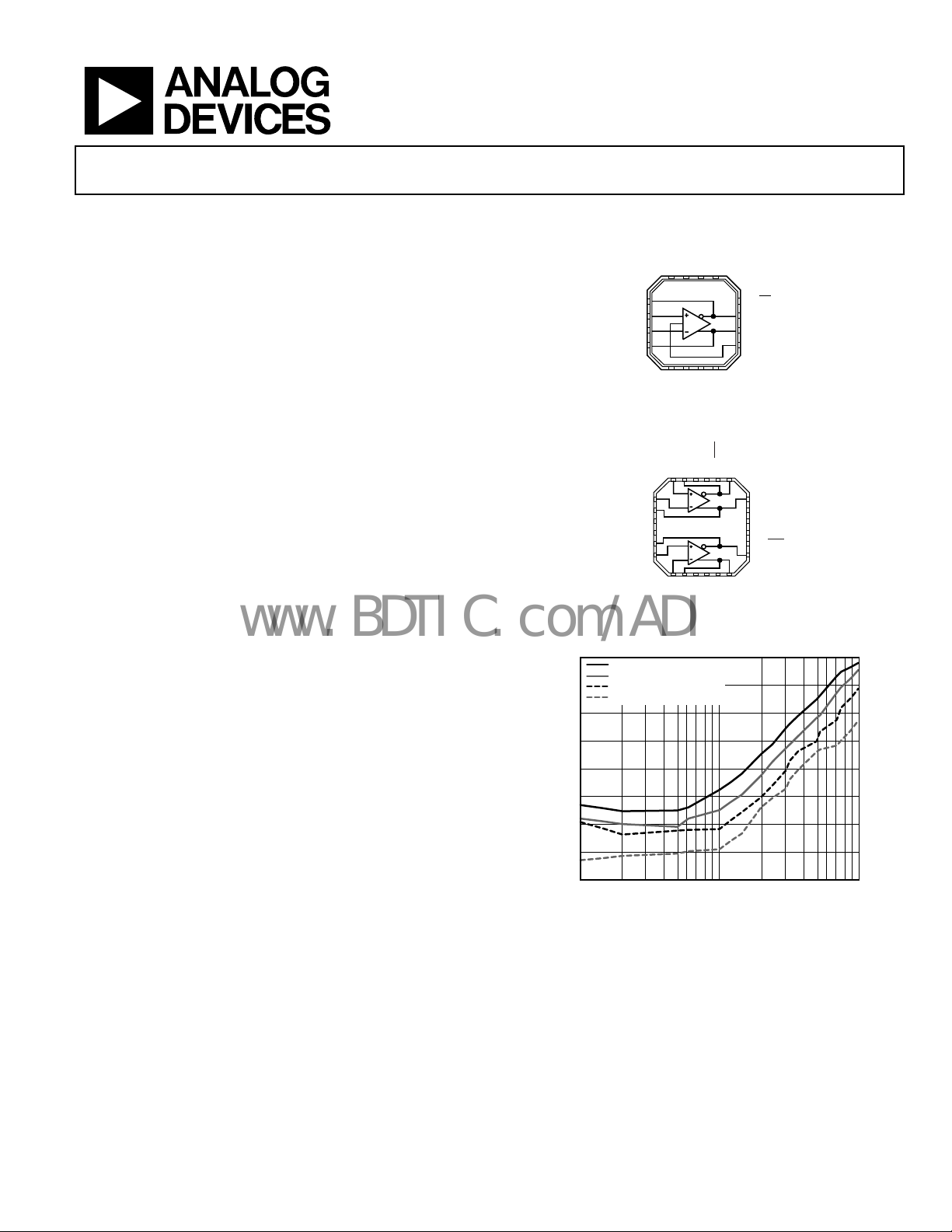
ADA4938-1/ADA4938-2
FUNCTIONAL BLOCK DIAGRAMS
S
S
S
S
–V
–V
–V
–V
14
13
15
16
ADA4938-1
1–FB
2+IN
3–IN
4+FB
5
6
S
S
+V
+V
Figure 1. ADA4938-1 Functional Block Diagram
1
N1
–FB
+I
23
24
1–IN1
2+FB1
3+V
S1
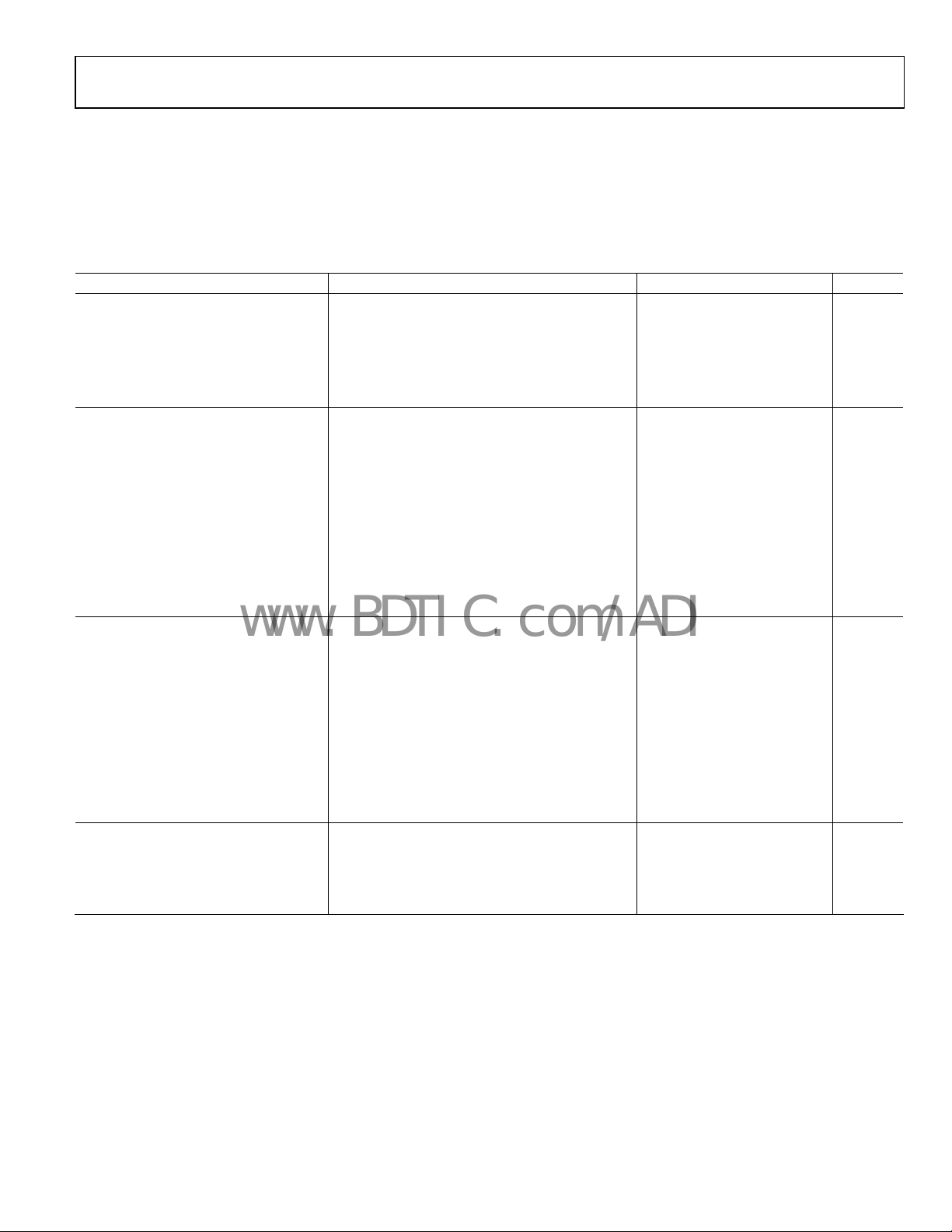
ADA4938-2
4+V
S1
5–FB2
6+IN2
7
8
2
–IN2
+FB
Figure 2. ADA4938-2 Functional Block Diagram
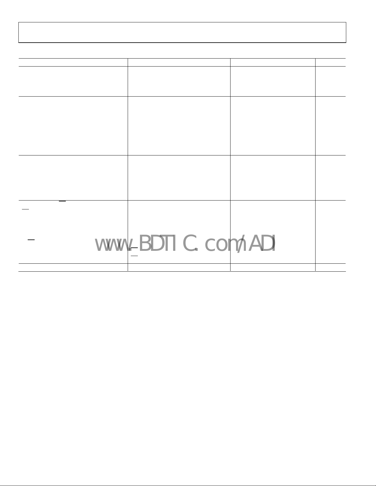
50
–60
–70
–80
–90
SFDR (dBc)
–100
–110
–120
–130
G = +2, V
G = +2, V
G = +2, V
G = +2, V
1 10 100
= 5V p-p
O, dm
= 3.2V p-p
O, dm
= 2V p-p
O, dm
= 1V p-p
O, dm
FREQUENCY (MHz )
Figure 3. SFDR vs. Freque
The ADA4938-1 (single amplifier) is available in a Pb-free,
3 mm × 3 mm, 16-lead LFCSP. The ADA4938-2 (dual
amplifier) is available in a Pb-free, 4 mm × 4 mm, 24-lead
LFCSP. The pinouts have been optimized to facilitate layout and
minimize distortion. The parts are specified to operate over the
extended industrial temperature range of −40°C to +85°C.
12 PD
11 –OUT
10 +OUT
9V
OCM
8
7
S
S
+V
+V
S1
S1
D1
–V
–V
P
–OUT1
20
19
21
22
9
11
12
10
S2
S2
CM2
+V
+V
O
V
+OUT2
18 +O UT1
17 V
OCM1
16 –V
S2
–V
15
S2
14
PD2
13 –O UT2
06592-001
6592-202
ncy and Output Voltage
06592-002
Rev. 0
Information furnished by Analog Devices is believed to be accurate and reliable. However, no
responsibility is assumed by Anal og Devices for its use, nor for any infringements of patents or ot her
rights of third parties that may result from its use. Specifications subject to change without notice. No
license is granted by implication or otherwise under any patent or patent rights of Analog Devices.
Trademarks and registered trademarks are the property of their respective owners.
One Technology Way, P.O. Box 9106, Norwood, MA 02062-9106, U.S.A.
Tel: 781.329.4700 www.analog.com
Fax: 781.461.3113 ©2007 Analog Devices, Inc. All rights reserved.

ADA4938-1/ADA4938-2
www.BDTIC.com/ADI
TABLE OF CONTENTS
Features .............................................................................................. 1
Applications....................................................................................... 1
General Description .........................................................................1
Functional Block Diagrams............................................................. 1
Revision History ............................................................................... 2
Specifications..................................................................................... 3
Dual-Supply Operation ............................................................... 3
Single-Supply Operation ............................................................. 5
Absolute Maximum Ratings............................................................ 7
Thermal Resistance ...................................................................... 7
ESD Caution.................................................................................. 7
Pin Configurations and Function Descriptions ...........................8
Typical Performance Characteristics............................................. 9
Test Circ uts ...................................................................................... 17
Operational Description................................................................ 18
Definition of Terms.................................................................... 18
Theory of Operation ...................................................................... 19
Analyzing an Application Circuit............................................ 19
Setting the Closed-Loop Gain .................................................. 19
Estimating the Output Noise Voltage...................................... 19
The Impact of Mismatches in the Feedback Networks......... 20
Calculating the Input Impedance of an
Application Circuit..................................................................... 20
Input Common-Mode Voltage Range in Single-Supply
Applications................................................................................ 20
Terminating a Single-Ended Input .......................................... 21
Setting the Output Common-Mode Voltage.......................... 21
Layout, Grounding, and Bypassing.............................................. 23
High Performance ADC Driving ................................................. 24
Outline Dimensions .......................................................................25
Ordering Guide .......................................................................... 25
REVISION HISTORY
11/07—Revision 0: Initial Version
Rev. 0 | Page 2 of 28
ADA4938-1/ADA4938-2
www.BDTIC.com/ADI
SPECIFICATIONS
DUAL-SUPPLY OPERATION
TA = 25°C, +VS = 5 V, −VS = −5 V, V
All specifications refer to single-ended input and differential output, unless otherwise noted. For gains other than G = 1, values for R
R
are shown in Ta ble 11.
G
= 0 V, RT = 61.9 , RG = RF = 200 , G = +1, R
OCM
= 1 kΩ, unless otherwise noted.
L, dm
and
F
Table 1. ±D
to ±OUT Performance
IN
Parameter Conditions Min Typ Max Unit
DYNAMIC PERFORMANCE
−3 dB Small Signal Bandwidth V
Bandwidth for 0.1 dB Flatness V
Large Signal Bandwidth V
Slew Rate V
= 0.1 V p-p 1000 MHz
OUT
= 2 V p-p 150 MHz
OUT
= 2 V p-p 800 MHz
OUT
= 2 V p-p 4700 V/μs
OUT
Overdrive Recovery Time VIN = 5 V to 0 V step, G = +2 4 ns
NOISE/HARMONIC PERFORMANCE
Second Harmonic V
V
Third Harmonic V
V
= 2 V p-p, 10 MHz −106 dBc
OUT
= 2 V p-p, 50 MHz −82 dBc
OUT
= 2 V p-p, 10 MHz −109 dBc
OUT
= 2 V p-p, 50 MHz −82 dBc
OUT
IMD f1 = 30.0 MHz, f2 = 30.1 MHz 89 dBc
IP3 f = 30 MHz, R
= 100 Ω 45 dBm
L, dm
Input Voltage Noise f = 10 MHz 2.6 nV/√Hz
Noise Figure G = +4, f = 10 MHz 15.8 dB
Input Current Noise f = 10 MHz 4.8 pA/√Hz
Crosstalk (ADA4938-2) f = 100 MHz −85 dB
INPUT CHARACTERISTICS
Offset Voltage V
T
OS, dm
MIN
= V
to T
/2; V
= V
OUT, dm
variation ±4 μV/°C
MAX
DIN+
= 0 V 1 4 mV
DIN−
Input Bias Current −18 −13 μA
T
MIN
to T
variation −0.01 μA/°C
MAX
Input Resistance Differential 6 MΩ
Common mode 3 MΩ
Input Capacitance 1 pF
Input Common-Mode Voltage
CMRR ∆V
OUT, dm
/∆V
IN, cm
; ∆V
= ±1 V, f = 1 MHz −75 dB
IN, cm
−V
+V
S
S
+ 0.3 to
− 1.6
V
OUTPUT CHARACTERISTICS
Output Voltage Swing Maximum ∆V
; single-ended output
OUT
−V
+V
S
S
+ 1.2 to
− 1.2
V
Linear Output Current Per amplifier 95 mA
Output Balance Error ∆V
OUT, cm
/∆V
OUT, dm
; ∆V
= 1 V; f = 10 MHz −60 dB
OUT, dm
Rev. 0 | Page 3 of 28
ADA4938-1/ADA4938-2
www.BDTIC.com/ADI
Table 2. V
Parameter Conditions Min Typ Max Unit
V
DYNAMIC PERFORMANCE
OCM
−3 dB Bandwidth 230 MHz
Slew Rate VIN = −3.4 V to +3.4 V, 25% to 75% 1700 V/μs
Input Voltage Noise (RTI) 7.5 nV/√Hz
V
INPUT CHARACTERISTICS
OCM
Input Voltage Range
Input Resistance 10 kΩ
Input Offset Voltage V
Input Bias Current 0.5 μA
V
OCM
Gain ∆V
POWER SUPPLY
Operating Range 4.5 11 V
Quiescent Current Per amplifier 37 40 mA
T
Powered down 2.0 3.0 mA
Power Supply Rejection Ratio ∆V
POWER DOWN (PD)
PD Input Voltage
Enabled ≥3 V
Turn-Off Time 1 μs
Turn-On Time 200 ns
PD Bias Current
Enabled
Disabled
OPERATING TEMPERATURE RANGE −40 +85 °C
to ±OUT Performance
OCM
CMRR ∆V
Powered down ≤2.5 V
PD
PD
+ 1.3 to
−V
S
− 1.3
+V
S
OS, cm
OUT, dm
OUT, cm
to T
MIN
OUT, dm
= 5 V
= −5 V
= V
; V
= V
OUT, cm
DIN+
/∆V
; ∆V
OCM
OCM
/∆V
; ∆V
OCM
OCM
variation 40 μA/°C
MAX
= 0 V 3 mV
DIN−
= ±1 V −81 dB
= ±1 V 0.95 1.00 1.05 V/V
/∆VS; ∆VS = ±1 V −80 dB
1 μA
−760 μA
V
Rev. 0 | Page 4 of 28
ADA4938-1/ADA4938-2
www.BDTIC.com/ADI
SINGLE-SUPPLY OPERATION
TA = 25°C, +VS = 5 V, −VS = 0 V, V
All specifications refer to single-ended input and differential output, unless otherwise noted. For gains other than G = 1, values for R
R
are shown in Ta ble 11.
G
= +VS/2, RT = 61.9 , RG = RF = 200 , G = +1, R
OCM
= 1 kΩ, unless otherwise noted.
L, dm
and
F
Table 3. ±D
to ±OUT Performance
IN
Parameter Conditions Min Typ Max Unit
DYNAMIC PERFORMANCE
−3 dB Small Signal Bandwidth V
Bandwidth for 0.1 dB Flatness V
Large Signal Bandwidth V
Slew Rate V
= 0.1 V p-p 1000 MHz
OUT
= 2 V p-p 150 MHz
OUT
= 2 V p-p 750 MHz
OUT
= 2 V p-p 3900 V/μs
OUT
Overdrive Recovery Time VIN = 2.5 V to 0 V step, G = +2 4 ns
NOISE/HARMONIC PERFORMANCE
Second Harmonic V
V
Third Harmonic V
V
= 2 V p-p, 10 MHz −110 dBc
OUT
= 2 V p-p, 50 MHz −79 dBc
OUT
= 2 V p-p, 10 MHz −100 dBc
OUT
= 2 V p-p, 50 MHz −79 dBc
OUT
Input Voltage Noise f = 10 MHz 2.6 nV/√Hz
Noise Figure G = +4, f = 10 MHz 15.8 dB
Input Current Noise f = 10 MHz 4.8 pA/√Hz
Crosstalk (ADA4938-2) f = 100 MHz −85 dB
INPUT CHARACTERISTICS
Offset Voltage V
T
OS, dm
MIN
= V
to T
/2; V
= V
= V
OUT, dm
variation ±4 μV/°C
MAX
DIN+
DIN−
= 2.5 V 1 4 mV
OCM
Input Bias Current −18 −13 μA
T
MIN
to T
variation −0.01 μA/°C
MAX
Input Resistance Differential 6 MΩ
Common mode 3 MΩ
Input Capacitance 1 pF
Input Common-Mode Voltage
CMRR ∆V
OUT, dm
/∆V
IN, cm
; ∆V
= ±1 V −80 dB
IN, cm
−V
+V
+ 0.3 to
S
− 1.6
S
V
OUTPUT CHARACTERISTICS
Output Voltage Swing Maximum ∆V
; single-ended output
OUT
−V
+V
+ 1.2 to
S
− 1.2
S
V
Linear Output Current Per amplifier 95 mA
Output Balance Error ∆V
OUT, cm
/∆V
OUT, dm
; ∆V
= 1 V −60 dB
OUT, dm
Rev. 0 | Page 5 of 28
ADA4938-1/ADA4938-2
www.BDTIC.com/ADI
Table 4. V
Parameter Conditions Min Typ Max Unit
V
DYNAMIC PERFORMANCE
OCM
−3 dB Bandwidth 400 MHz
Slew Rate VIN = 1.6 V to 3.4 V, 25% to 75% 1700 V/μs
Input Voltage Noise (RTI) 7.5 nV/√Hz
V
INPUT CHARACTERISTICS
OCM
Input Voltage Range
Input Resistance 10 kΩ
Input Offset Voltage V
Input Bias Current 0.5 μA
V
OCM
Gain ∆V
POWER SUPPLY
Operating Range 4.5 11 V
Quiescent Current 34 36.5 mA
T
Powered down 1.0 1.7 mA
Power Supply Rejection Ratio ∆V
POWER DOWN (PD)
PD Input Voltage
Enabled ≥3 V
Turn-Off Time 1 μs
Turn-On Time 200 ns
PD Bias Current
Enabled
Disabled
OPERATING TEMPERATURE RANGE −40 +85 °C
to ±OUT Performance
OCM
CMRR ∆V
Powered down ≤2.5 V
PD
PD
+ 1.3 to
−V
S
− 1.3
+V
S
OS, cm
OUT, dm
OUT, cm
to T
MIN
OUT, dm
= 5 V
= 0 V
= V
; V
= V
= V
OUT, cm
DIN+
DIN–
/∆V
; ∆V
OCM
/∆V
OCM
variation 40 μA/°C
MAX
= ±1 V −89 dB
OCM
; ∆V
= ±1 V 0.95 1.00 1.05 V/V
OCM
= 2.5 V 3 mV
OCM
/∆VS; ∆VS = ±1 V −80 dB
1 μA
−260 μA
V
Rev. 0 | Page 6 of 28
ADA4938-1/ADA4938-2
www.BDTIC.com/ADI
ABSOLUTE MAXIMUM RATINGS
Table 5.
Parameter Rating
Supply Voltage 12 V
Power Dissipation See Figure 4
Storage Temperature Range −65°C to +125°C
Operating Temperature Range −40°C to +85°C
Lead Temperature (Soldering, 10 sec) 300°C
Junction Temperature 150°C
Stresses above those listed under Absolute Maximum Rating
may cause permanent damage to the device. This is a stress
rating only; functional operation of the device at these or any
other conditions above those indicated in the operational
section of this specification is not implied. Exposure to absolute
maximum rating conditions for extended periods may affect
device reliability.
THERMAL RESISTANCE
θJA is specified for the device (including exposed pad) soldered
to a high thermal conductivity 4-layer circuit board, as described in
EIA/JESD 51-7. The exposed pad is not electrically connected to
the device. It is typically soldered to a pad on the PCB that is
thermally and electrically connected to an internal ground plane.
Table 6. Thermal Resistance
Package Type θ
JA
16-Lead LFCSP (Exposed Pad) 95 °C/W
24-Lead LFCSP (Exposed Pad) 65 °C/W
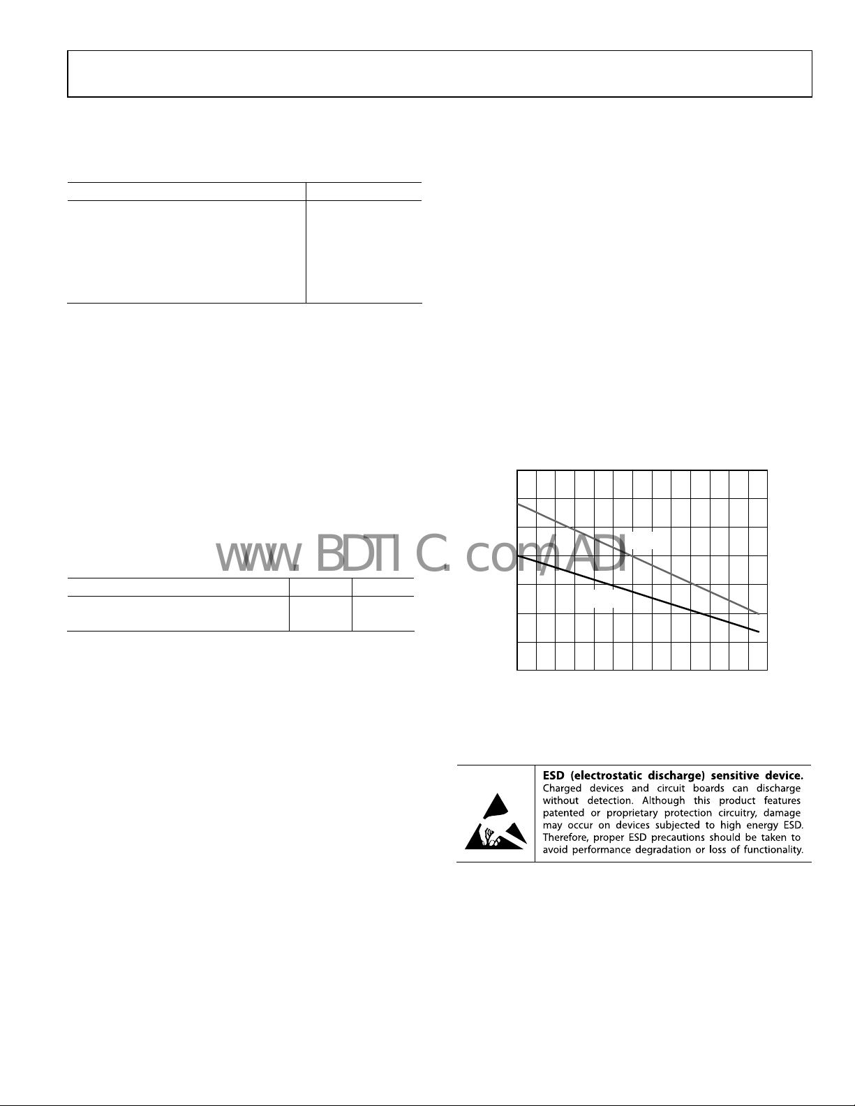
Maximum Power Dissipation
The maximum safe power dissipation in the ADA4938 package
is limited by the associated rise in junction temperature (T
the die. At approximately 150°C, which is the glass transition
temperature, the plastic changes its properties. Even temporarily
exceeding this temperature limit can change the stresses that the
package exerts on the die, permanently shifting the parametric
performance of the ADA4938. Exceeding a junction temperature of
150°C for an extended period can result in changes in the silicon
devices, potentially causing failure.
Unit
) on
J
The power dissipated in the package (P
quiescent power dissipation and the power dissipated in the
package due to the load drive. The quiescent power is the voltage
between the supply pins (V
) times the quiescent current (IS).
S
The power dissipated due to the load drive depends upon the
particular application. The power due to load drive is calculated
by multiplying the load current by the associated voltage drop
across the device. RMS voltages and currents must be used in
these calculations.
Airflow increases heat dissipation, which effectively reducing
. In addition, more metal directly in contact with the package
θ
JA
leads/exposed pad from metal traces, through-holes, ground,
and power planes reduces the θ
JA
Figure 4 shows the maximum safe power dissipation in the
ackage vs. the ambient temperature for the 16-lead LFCSP
p
(95°C/W) and the 24-lead LFCSP (65°C/W) on a JEDEC standard
4-layer board.
3.5
3.0
2.5
ADA4938-2
2.0
1.5
1.0
MAXIMUM POWER DISSIPATION (W)
0.5
0
–40 –30 –20 –10 0 10 20 30 40 50 60 70 80 90
Figure 4. Maximum Power Dissipation vs. Temperature for a 4-Layer Board
ADA4938-1
AMBIENT TEMPERATURE (°C)
ESD CAUTION
) is the sum of the
D
.
06592-103
Rev. 0 | Page 7 of 28
ADA4938-1/ADA4938-2
www.BDTIC.com/ADI
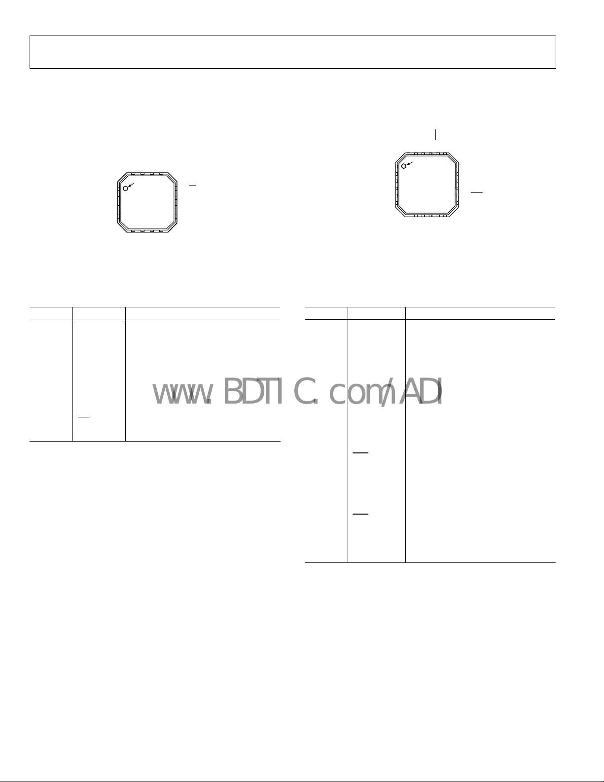
PIN CONFIGURATIONS AND FUNCTION DESCRIPTIONS
–OUT1
–VS1–VS1–FB1
+IN1
S
S
S
S
–V
–V
–V
–V
14
13
15
16
PIN 1
1–FB
2+IN
ADA4938-1
3–IN
(Not to Scal e)
4+FB
INDICATOR
TOP VIEW
5
6
S
S
+V
+V
12 PD
11 –OUT
10 +OUT
9V
OCM
8
7
S
S
+V
+V
Figure 5. ADA4938-1 Pin Configuration
06592-003
1
–IN1
2
+FB1
3
+V
+V
–FB2
+IN2
S1
S1
ADA4938-2
4
5
6
(Not to S cale)
Figure 6. ADA4938-2 Pin Configuration
24
23
22
PIN 1
INDICATO R
TOP VIEW
9
7
8
S2
–IN2
+V
+FB2
PD1
19
20
21
18
+OUT1
V
17
OCM1
16
–V
S2
–V
15
S2
14
PD2
–OUT2
13
10
12
11
S2
+V
OCM2
V
+OUT2
06592-206
Table 7. ADA4938-1 Pin Function Descriptions
Pin No. Mnemonic Description
1 −FB Negative Output Feedback Pin.
2 +IN Positive Input Summing Node.
3 −IN Negative Input Summing Node.
4 +FB Positive Output Feedback Pin.
5 to 8 +V
9 V
S
OCM
Positive Supply Voltage.
Output Common-Mode Voltage.
10 +OUT Positive Output for Load Connection.
11 −OUT Negative Output for Load Connection.
12
PD
13 to 16 −V
S
Power-Down Pin.
Negative Supply Voltage.
Table 8. ADA4938-2 Pin Function Descriptions
Pin No. Mnemonic Description
1 −IN1 Negative Input Summing Node 1.
2 +FB1 Positive Output Feedback Pin 1.
3, 4 +V
S1
5 −FB2
6 +IN2
7 −IN2
8 +FB2
9, 10 +V
11 V
S2
OCM2
12 +OUT2
13 −OUT2
14
15, 16
17
PD2
−V
V
OCM1
S2
18 +OUT1
19 −OUT1
20
21, 22 −V
PD1
S1
23 −FB1
Positive Supply Voltage 1.
Negative Output Feedback Pin 2.
Positive Input Summing Node 2.
Negative Input Summing Node 2.
Positive Output Feedback Pin 2.
Positive Supply Voltage 2.
Output Common-Mode Voltage 2.
Positive Output 2.
Negative Output 2.
Power-Down Pin 2.
Negative Supply Voltage 2.
Output Common-Mode Voltage 1.
Positive Output 1.
Negative Output 1.
Power-Down Pin 1.
Negative Supply Voltage 1.
Negative Output Feedback Pin 1.
24 +IN1 Positive Input Summing Node 1.
Rev. 0 | Page 8 of 28
ADA4938-1/ADA4938-2
www.BDTIC.com/ADI
TYPICAL PERFORMANCE CHARACTERISTICS
TA = 25°C, +VS = 5 V, −VS = −5 V, V
All measurements were performed with single-ended input and differential output, unless otherwise noted. For gains other than G = +1,
values for R
and RG are shown in Ta ble 11.
F
3
= 0 V, RT = 61.9 , RG = RF = 200 , G = +1, R
OCM
= 1 kΩ, unless otherwise noted.
L, dm
3
0
–3
–6
NORMALIZE D GAIN (dB)
–9
–12
G = +1
G = +2
G = +3.16
G = +5
1 10 100 1000
FREQUENCY (MHz)
Figure 7. Small Signal Frequency Response for Various Gains, V
3
0
–3
GAIN (dB)
–6
–9
VS = +5V
–12
Figu re 8. Small Signal Response for Various Supplies, V
VS = ±5V
1 10 100 1000
FREQUENCY (MHz)
OUT
3
= 0.1 V p-p
OUT
= 0.1 V p-p
0
–3
–6
NORMALIZE D GAIN (dB)
–9
–12
06592-105
G = +1
G = +2
G = +3.16
G = +5
1 10 100 1000
FREQUENCY (MHz)
06592-108
Figure 10. Large Signal Frequency Response for Various Gains
3
0
–3
GAIN (dB)
–6
–9
VS = +5V
–12
06592-106
VS = ±5V
1 10 100 1000
FREQUENCY (MHz)
06592-109
Figure 11. Large Signal Response for Various Supplies
3
0
–3
–6
NORMALIZE D GAIN (dB)
–9
–12
–40°C
+25°C
+85°C
1 10 100 1000
Figure 9. Small Signal Fr
Various Temperatures, V
FREQUENCY (MHz)
equency Response for
= 0.1 V p-p
OUT
06592-107
Rev. 0 | Page 9 of 28
0
–3
–6
NORMALIZE D GAIN (dB)
–9
–12
–40°C
+25°C
+85°C
1 10 100 1000
FREQUENCY (MHz)
Figure 12. Large Signal Frequency Response for Various Temperatures
06592-110

ADA4938-1/ADA4938-2
www.BDTIC.com/ADI
3
3
0
–3
–6
–9
–12
NORMALIZE D GAIN (dB)
–15
–18
–21
RL = 1kΩ
RL = 100Ω
RL = 200Ω
1 10 100 1000
FREQUENCY (MHz)
Figure 13. Small Signal Frequency Response for
V
arious Loads, V
3
0
–3
–6
NORMALIZE D GAIN (dB)
–9
–12
G = +1
G = +2
G = +3.16
G = +5
1 10 100 1000
FREQUENCY (MHz)
= 0.1 V p-p
OUT
Figure 14. Small Signal Frequency Response for
Va
rious Gains, V
6
= 5 V, V
S
= 0.1 V p-p
OUT
0
–3
–6
–9
–12
NORMALIZE D GAIN (dB)
–15
–18
–21
06592-111
RL = 1kΩ
RL = 100Ω
RL = 200Ω
1 10 100 1000
FREQUENCY (MHz)
06592-114
Figure 16. Large Signal Frequency Response for Various Loads
3
0
–3
–6
NORMALIZE D GAIN (dB)
–9
–12
06592-112
Figure 17. Large Signal Frequency Response for Various Gains, V
G = +1
G = +2
G = +3.16
G = +5
1 10 100 1000
FREQUENCY (MHz)
= 5 V
S
06592-115
6
3
0
–3
–6
NORMALIZE D GAIN (dB)
–9
–12
Figure 15. Small Signal Response for Various Gains, R
G = +1
G = +2
G = +3.16
G = +5
1 10 100 1000
FREQUENCY (MHz)
= 402 Ω, V
F
= 0.1 V p-p
OUT
06592-113
Rev. 0 | Page 10 of 28
3
0
–3
–6
NORMALIZE D GAIN (dB)
–9
–12
G = +1
G = +2
G = +3.16
G = +5
1 10 100 1000
FREQUENCY (MHz)
Figure 18. Large Signal Response for Various Gains, R
= 402 Ω
F
06592-116

ADA4938-1/ADA4938-2
www.BDTIC.com/ADI
6
6
3
0
–3
–6
NORMALIZE D GAIN (dB)
–9
–12
G = +1
G = +2
G = +3.16
G = +5
1 10 100 1000
FREQUENCY (MHz)
Figure 19. Small Signal Frequency Response for Various Gains, R
= 5 V, V
V
S
3
0
–3
GAIN (dB)
–6
–9
= 0.1 V p-p
OUT
06592-117
= 402 Ω,
F
3
0
–3
–6
NORMALIZE D GAIN (dB)
–9
–12
Figure 22. Large Signal Frequency Response for Various Gains, R
3
0
–3
GAIN (dB)
–6
–9
G = +1
G = +2
G = +3.16
G = +5
1 10 100 1000
FREQUENCY (MHz)
= 5 V
V
S
06592-120
= 402 Ω,
F
VS = +5V
–12
Figure 20. V
VS = ±5V
1 10 100 1000
OUT, cm
FREQUENCY (MHz)
Small Signal Frequency Response, V
= 0.1 V p-p
OUT
1.0
0.9
0.8
0.7
0.6
0.5
0.4
0.3
0.2
0.1
0
–0.1
–0.2
–0.3
–0.4
NORMALIZE D GAIN (dB)
–0.5
–0.6
–0.7
–0.8
–0.9
–1.0
R
= 1kΩ
L, dm
R
= 100Ω
L, dm
R
= 200Ω
L, dm
1 10 100 1000
FREQUENCY (MHz)
Figure 21. 0.1 dB Flatness Response for Various Loads, ADA4938-1,
= 0.1 V p-p
V
OUT
VS = +5V
–12
06592-118
VS = ±5V
1 10 100 1000
Figure 23. V
FREQUENCY (MHz)
Large Signal Frequency Response
OUT, cm
06592-121
1.5
1.4
1.3
1.2
1.1
1.0
0.9
0.8
0.7
0.6
0.5
0.4
GAIN (dB)
0.3
0.2
0.1
0
–0.1
–0.2
–0.3
–0.4
–0.5
06592-119
R
= 1kΩ
L, dm
R
= 100Ω
L, dm
R
= 200Ω
L, dm
1 10 100 1000
FREQUENCY (MHz)
06592-122
Figure 24. 0.1 dB Flatness Response for Various Loads, ADA4938-2,
= 0.1 V p-p
V
OUT
Rev. 0 | Page 11 of 28

ADA4938-1/ADA4938-2
–
–
–
–
–
–
www.BDTIC.com/ADI
–50
–60
40
HD2, VS = +5V
HD3, VS = +5V
HD2, VS = ±5V
HD3, VS = ±5V
–50
–60
40
HD2, +5V
HD3, +5V
HD2, ±5V
HD3, ±5V
–70
–80
–90
DISTORT ION (dBc)
–100
–110
–120
1 10 100
FREQUENCY (MHz)
Figure 25. Harmonic Distortion vs. Frequency and Supply Voltage
–100
DISTORT ION (dBc)
–110
–120
–130
40
–50
–60
–70
–80
–90
HD2, G = +1
HD3, G = +1
HD2, G = +2
HD3, G = +2
HD2, G = +5
HD3, G = +5
1 10 100
FREQUENCY (MHz )
Figure 26. Harmonic Distortion vs. Frequency and Gain
40
–50
–60
–70
–80
–90
–100
DISTORT ION (dBc)
–110
–120
–130
–3.3 –2.7 –2.1 –1.5 –0.9 –0.3 0.3 0.9 1.5 2.1 2.7 3.3
Figure 27. Harmonic Distortion vs. V
HD2, 10MHz
HD3, 10MHz
HD2, 70MHz
HD3, 70MHz
V
(V)
OCM
and Frequency
OCM
–70
–80
–90
DISTORT ION (dBc)
–100
–110
–120
0987654312
06592-123
Figure 28. Harmonic Distortion vs. V
V
OUT, dm
(V)
and Supply Voltage
OUT
06592-126
40
HD2, RL = 1kΩ
–50
–60
–70
–80
–90
DISTORT ION (dBc)
–100
–110
–120
06592-124
HD3, RL = 1kΩ
HD2, RL = 200Ω
HD3, RL = 200Ω
HD2, RL = 100Ω
HD3, RL = 100Ω
1 10 100
FREQUENCY (MHz)
06592-127
Figure 29. Harmonic Distortion vs. Frequency for Various Loads
40
–50
–60
–70
–80
–90
DISTORT ION (dBc)
–100
–110
–120
1.7 3.33. 12.92.72.52.32.11.9
06592-128
Figure 30. Harmonic Distortion vs. V
HD2, 10MHz
HD3, 10MHz
HD2, 70MHz
HD3, 70MHz
V
(V)
OCM
OCM
and Frequency, VS = 5 V
06592-125
Rev. 0 | Page 12 of 28

ADA4938-1/ADA4938-2
–
–
–
www.BDTIC.com/ADI
10
0
–10
–20
–30
–40
–50
–60
–70
DISTORT ION (dBc)
–80
–90
–100
–110
29.5 30.530.430.330.230.130.029. 929.829.729.6
20
–25
–30
–35
–40
–45
–50
–55
CMRR (dB)
IN
–60
V
–65
–70
–75
–80
–85
0.1 1000100101
15
RL = 200Ω
–20
–25
–30
–35
–40
–45
–50
OUTPUT BALANCE (dB)
–55
–60
–65
1 100010010
FREQUENCY (MHz)
Figure 31. Intermodulation Distortion
V
= ±5V
S
VS = +5V
FREQUENCY (MHz )
Figure 32. V
CMRR vs. Frequency
IN
FREQUENCY (MHz )
Figure 33. Output Balance vs. Frequency
06592-129
06592-130
06592-131
0
–5
–10
–15
–20
–25
–30
–35
–40
–45
–50
PSRR (d B)
–55
–60
–65
–70
–75
–80
–85
0.1 1000100101
–PSRR
+PSRR
FREQUENCY (MHz )
Figure 34. PSRR vs. Frequency
0
–5
–10
–15
–20
–25
–30
–35
RETURN LOSS (d B)
–40
–45
–50
–55
1 10 100 1000
FREQUENCY (MHz)
S22
S11
Figure 35. Return Loss (S11, S22) vs. Frequency
SFDR (dBc)
40
–50
–60
–70
–80
–90
–100
–110
–120
RL = 1kΩ
RL = 200Ω
RL = 100Ω
1 10 100
FREQUENCY (MHz)
Figure 36. SFDR vs. Frequency for Various Loads
06592-132
06592-134
06592-135
Rev. 0 | Page 13 of 28

ADA4938-1/ADA4938-2
www.BDTIC.com/ADI
26
24
G = +1
22
20
G = +2
18
G = +4
16
NOISE FIGURE (dB)
14
12
100
10
INPUT VOLTAGE NOISE (nV/ Hz)
10
10 500100
FREQUENCY (MHz )
Figure 37. Noise Figure vs. Frequen
10
8
6
4
2
0
–2
VOLTAGE (V)
–4
–6
060555045403530252015105
VIN × 3.16
V
, dm
OUT
TIME (5ns/DIV)
–8
–10
Figure 38. Overdrive Recovery T
12
10
8
6
4
2
0
–2
VOLTAGE (V)
–4
–6
–8
050045040035030025020015010050
VIN × 3.16
V
, dm
OUT
TIME (50n s/DIV)
–10
–12
Figure 39. Overdrive Amplitude Character
cy
ime (Pulse Input)
istics (Triangle Wave Input)
1
10 100 1k 10k 100M100k 1M 10M
06592-136
FREQUENCY (Hz)
06592-039
Figure 40. Input Voltage Noise vs. Frequency
4.0
3.5
3.0
2.5
2.0
1.5
VOLTAGE (V)
1.0
0.5
0
–0.5
06592-137
PD INPUT
SINGLE O UTPUT
TIME (200ns/DIV)
06592-140
Figure 41. Power-Down Response Time
45
40
35
30
25
20
CURRENT (mA)
15
10
06592-138
+85°C
+25°C
–40°C
5
0
2.0 2.2 2.4 2.6 2.8 3.0 3.2 3.4 3.6 3. 8 4.0
VOLTAGE (V)
06592-141
Figure 42. Supply Current vs. Power-Down Voltage and Temperature
Rev. 0 | Page 14 of 28

ADA4938-1/ADA4938-2
www.BDTIC.com/ADI
0.20
0.15
0.10
0.05
0
VOLTAGE (V)
–0.05
–0.10
–0.15
–0.20
TIME (1ns/DIV)
Figure 43. Small Signal Transient Response, V
0.10
0.08
0.06
0.04
0.02
0
–0.02
VOLTAGE (V)
–0.04
–0.06
–0.08
–0.10
Figure 44. V
Small Signal Transient Response, V
OCM
TIME (2ns/DIV)
60
50
+85°C
+25°C
–40°C
= 0.1 V p-p
OUT
= 0.1 V p-p
OUT
06592-142
06592-043
3.0
2.5
2.0
1.5
1.0
0.5
0
–0.5
VOLTAGE (V)
–1.0
–1.5
–2.0
–2.5
–3.0
2.5
2.0
1.5
1.0
0.5
0
–0.5
VOLTAGE (V)
–1.0
–1.5
–2.0
–2.5
3
ALL CURVES ARE
NORMALIZED T O V
0
TIME (1ns/DIV)
Figure 46. Large Signal Transient Response
TIME (2ns/DIV)
Figure 47. V
Large Signal Transient Response
OCM
= 0V
OCM
06592-145
06592-046
40
30
CURRENT (mA)
20
10
0
2.0 2.2 2.4 2.6 2.8 3.0 3.2 3.4 3.6 3.8 4.0
Figure 45. Supply Current vs. Power-Down Voltage and Temperature, V
VOLTAGE (V)
= 5 V
S
06592-144
Rev. 0 | Page 15 of 28
–3
V
–6
CLOSED-LOOP GAIN (dB)
–9
–12
1 10 100 1000
Figure 48. V
Small Signal Frequency Response for Various V
OUT, dm
FREQUENCY (MHz)
V
OUT
= –3.7V
OCM
V
= –3.5V
OCM
V
= –3V
OCM
V
= 0V
OCM
V
= +3V
OCM
V
= +3.5V
OCM
V
= +3.7V
OCM
= 0.1 V p-p
OCM
06592-048
,

ADA4938-1/ADA4938-2
–
www.BDTIC.com/ADI
55
50
100
45
IP3 (dBm)
40
35
30
10 100
IP3 100Ω
FREQUENCY (M Hz)
Figure 49. IP3 vs. Frequency
3
ALL CURVES ARE
NORMALIZE D TO V
0
–3
–6
V
= –3.7V
OCM
V
= –3.5V
CLOSED-LOOP GAIN (dB)
–12
Figure 50. V
OCM
V
= –3V
OCM
–9
V
= 0V
OCM
V
= +3V
OCM
V
= +3.5V
OCM
V
= +3.7V
OCM
1 10 100 1000
Large Signal Frequency Response for Various V
OUT, dm
= 0V
OCM
FREQUENCY (MHz)
OCM
10
INPUT CURRENT NO ISE (pA/ Hz)
06592-049
1
10 100 1k 10k 100M100k 1M 10M
FREQUENCY (Hz)
06592-051
Figure 51. Input Current Noise vs. Frequency
40
–50
–60
–70
–80
–90
–100
CROSSTALK (dB)
–110
–120
–130
–140
0.3 1 10 100 1000
06592-50
Figure 52. Crosstalk vs. Frequency for ADA4938-2
FREQUENCY (MHz )
INPUT1, OUTPUT2
INPUT2, OUTPUT1
06592-888
Rev. 0 | Page 16 of 28

ADA4938-1/ADA4938-2
Ω
www.BDTIC.com/ADI
TEST CIRCUTS
200Ω
+5V
200Ω50Ω
V
IN
61.9Ω
V
OCM
200Ω
27.5Ω
ADA4938
–5V
200Ω
1kΩ
06592-246
Figure 53. Equivalent Basic Test Circuit
200Ω
+5V
200Ω50Ω
V
IN
61.9Ω
V
OCM
200Ω
27.5Ω
ADA4938
–5V
200Ω
50Ω
50Ω
06592-247
Figure 54. Test Circuit for Output Balance
200
+5V
FILTER
V
IN
61.9Ω
200Ω50Ω
V
OCM
200Ω
27.5Ω
ADA4938
–5V
200Ω
0.1µF
0.1µF
412Ω
412Ω
FILTER
6592-248
Figure 55. Test Circuit for Distortion Measurements
Rev. 0 | Page 17 of 28

ADA4938-1/ADA4938-2
–
V
www.BDTIC.com/ADI
OPERATIONAL DESCRIPTION
DEFINITION OF TERMS
FB
ADA4938
R
F
R
G
+IN
OCM
–IN
R
G
R
+FB
F
Figure 56. Circuit Definitions
Differential Voltage
The differential voltage is the difference between two node
voltages. For example, the output differential voltage (or
equivalently, output differential-mode voltage) is defined as
V
where V
OUT, dm
+OUT
= (V
and V
− V
+OUT
refer to the voltages at the +OUT and
−OUT
−OUT terminals with respect to a common reference.
−OUT
–OUT
V
R
OUT, dm
L, dm
+OUT
06592-004
)
Common-Mode Voltage
The common-mode voltage is the average of two node voltages.
The output common-mode voltage is defined as
V
OUT, cm
= (V
+OUT
+ V
−OUT
)/2
Balance
Balance is a measure of how well differential signals are matched in
amplitude and are exactly 180° apart in phase. Balance is most
easily determined by placing a well-matched resistor divider
between the differential voltage nodes and comparing the
magnitude of the signal at the midpoint of the divider with
the magnitude of the differential signal. By this definition,
output balance is the magnitude of the output common-mode
voltage divided by the magnitude of the output differential
mode voltage.
V
cmOUT
,
=
ErrorBalanceOutput
V
dmOUT
,
Rev. 0 | Page 18 of 28

ADA4938-1/ADA4938-2
V
V
www.BDTIC.com/ADI
THEORY OF OPERATION
The ADA4938 differs from conventional op amps in that it has
two outputs whose voltages move in opposite directions. Like
an op amp, it relies on open-loop gain and negative feedback
to force these outputs to the desired voltages. The ADA4938
behaves much like a standard voltage feedback op amp and
makes it easier to perform single-ended-to-differential conversions,
common-mode level shifting, and amplifications of differential
signals. Also like an op amp, the ADA4938 has high input
impedance and low output impedance.
Two feedback loops are employed to control the differential and
mmon-mode output voltages. The differential feedback, set
co
with external resistors, controls only the differential output
voltage. The common-mode feedback controls only the commonmode output voltage. This architecture makes it easy to set the
output common-mode level to any arbitrary value. It is forced,
by internal common-mode feedback, to be equal to the voltage
applied to the V
input, without affecting the differential
OCM
output voltage.
The ADA4938 architecture results in outputs that are highly
b
alanced over a wide frequency range without requiring tightly
matched external components. The common-mode feedback
loop forces the signal component of the output commonmode voltage to zero, which results in nearly perfectly balanced
differential outputs that are identical in amplitude and are
exactly 180° apart in phase.
ANALYZING AN APPLICATION CIRCUIT
The ADA4938 uses open-loop gain and negative feedback to
force its differential and common-mode output voltages in such
a way as to minimize the differential and common-mode error
voltages. The differential error voltage is defined as the voltage
between the differential inputs labeled +IN and −IN (see
Figure 56). For most purposes, this voltage can be assumed
o be zero. Similarly, the difference between the actual output
t
common-mode voltage and the voltage applied to V
be assumed to be zero. Starting from these two assumptions,
any application circuit can be analyzed.
can also
OCM
SETTING THE CLOSED-LOOP GAIN
The differential-mode gain of the circuit in Figure 56 can be
determined by
V
V
This assumes the input resistors (R
R
,
dmOUT
F
=
R
,
G
dmIN
) and feedback resistors (RF)
G
on each side are equal.
ESTIMATING THE OUTPUT NOISE VOLTAGE
The differential output noise of the ADA4938 can be estimated
using the noise model in Figure 57. The input-referred noise
tage density, v
vol
noise currents, i
ground. The noise currents are assumed to be equal and produce a
voltage across the parallel combination of the gain and feedback
resistances. v
Each of the four resistors contributes (4kTR)
the input noise sources, the multiplication factors, and the outputreferred noise density terms.
, is modeled as a differential input, and the
nIN
and i
nIN−
is the noise voltage density at the V
nCM
nRG1
R
G1
i
nIN+
i
nIN–
R
G2
V
nRG2
Figure 57. ADA4938 Noise Model
, appear between each input and
nIN+
1/2
. Table 9 summarizes
nRF1
R
F1
+
V
nIN
R
ADA4938
V
F2
V
OCM
nRF2
V
nOD
V
nCM
OCM
pin.
06592-005
Table 9. Output Noise Voltage Den
sity Calculations
Input Noise
Input Noise Contribution Input Noise Term
Differential Input v
Inverting Input i
Noninverting Input i
V
Input v
OCM
Gain Resistor, R
Gain Resistor, R
Feedback Resistor, R
Feedback Resistor, R
G1
G2
F1
F2
nIN
i
nIN−
i
nIN+
nCM
v
nRG1
v
nRG2
v
nRF1
v
nRF2
V
oltage Density
v
nIN
× (RG2||RF2) G
nIN−
× (RG1||RF1) G
nIN+
v
nCM
(4kTRG1)
(4kTRG2)
(4kTRF1)
(4kTRF2)
Rev. 0 | Page 19 of 28
Output
Multiplication Factor
G
N
N
N
GN(β1 − β2) v
1/2
1/2
1/2
1/2
GN(1 − β2) v
GN(1 − β1) v
1 v
1 v
Output Noise
Voltage Density Term
v
= GN(v
nO1
v
= GN[i
nO2
v
= GN[i
nO3
= GN(β1 − β2)(v
nO4
= GN(1 − β2)(4kTRG1)
nO5
= GN(1 − β1)(4kTRG2)
nO6
= (4kTRF1)
nO7
= (4kTRF2)
nO8
)
nIN
× (RG2||RF2)]
nIN−
× (RG1||RF1)]
nIN+
1/2
1/2
nCM
)
1/2
1/2

ADA4938-1/ADA4938-2
www.BDTIC.com/ADI
Similar to the case of a conventional op amp, the output noise
voltage densities can be estimated by multiplying the inputreferred terms at +IN and −IN by the appropriate output factor,
where:
2
=
N
β+=
1
When R
(
F1
is the circuit noise gain.
)
ββG+
21
R
G1
RR
F1/RG1
G1
β+=
and
= RF2/RG2, β1 = β2 = β, and the noise gain
R
G2
2
F2
are the feedback factors.
RR
G2
becomes
R
1
G +== 1
N
β
Note that the output noise from V
The total differential output noise density, v
F
R
G
goes to zero in this case.
OCM
, is the root-sum-
nOD
square of the individual output noise terms.
8
2
=
vv
∑
nOinOD
=
1i
THE IMPACT OF MISMATCHES IN THE FEEDBACK NETWORKS
As previously mentioned, even if the external feedback networks
(R
) are mismatched, the internal common-mode feedback
F/RG
loop still forces the outputs to remain balanced. The amplitudes
of the signals at each output remain equal and 180° out of phase.
The input-to-output, differential mode gain varies proportionately
to the feedback mismatch, but the output balance is unaffected.
As well as causing a noise contribution from V
errors in the external resistors result in a degradation of the
ability of the circuit to reject input common-mode signals, much
the same as for a four-resistor difference amplifier made from a
conventional op amp.
In addition, if the dc levels of the input and output commonm
ode voltages are different, matching errors result in a small
differential-mode output offset voltage. When G = +1, with a
ground referenced input signal and the output common-mode
level set to 2.5 V, an output offset of as much as 25 mV (1% of
the difference in common-mode levels) can result if 1% tolerance
resistors are used. Resistors of 1% tolerance result in a worst-case
input CMRR of about 40 dB, a worst-case differential-mode
output offset of 25 mV due to 2.5 V level-shift, and no significant
degradation in output balance error.
, ratio matching
OCM
CALCULATING THE INPUT IMPEDANCE OF AN APPLICATION CIRCUIT
The effective input impedance of a circuit depends on whether
the amplifier is being driven by a single-ended or differential
signal source. For balanced differential input signals, as shown
in Figure 58, the input impedance (R
and −DIN) is simply R
(+D
IN
R
+D
–D
Figure 58. ADA4938 Configured for Balanced (Differential) Inputs
G
IN
IN
V
R
G
IN, dm
ADA4938
+IN
OCM
–IN
= 2 × RG.
R
F
+V
S
R
F
) between the inputs
IN, dm
V
OUT, dm
06592-006
For an unbalanced, single-ended input signal (see Figure 59),
the input impedance is
⎛
⎜
⎜
=
R
cmIN
,
⎜
⎜
⎝
R
S
Figure 59. ADA4938 Configured for Unbalanced (Single-Ended) Input
R
G
R
T
R
S
V
OCM
R
G
R
T
R
G
1
R
−
()
2
R
F
+V
S
ADA4938
R
F
⎞
⎟
⎟
⎟
F
⎟
RR
+×
F
G
⎠
V
OUT, dm
06592-007
The input impedance of the circuit is effectively higher than it
would be for a conventional op amp connected as an inverter
because a fraction of the differential output voltage appears at
the inputs as a common-mode signal, partially bootstrapping
the voltage across the input resistor R
.
G
INPUT COMMON-MODE VOLTAGE RANGE IN SINGLE-SUPPLY APPLICATIONS
The ADA4938 is optimized for level-shifting, ground-referenced
input signals. As such, the center of the input common-mode
range is shifted approximately 1 V down from midsupply. The
input common-mode range at the summing nodes of the amplifier
is from 0.3 V above −V
the outputs, the voltage swing at the +IN and −IN terminals must
be confined to these ranges.
to 1.6 V below +VS. To avoid clipping at
S
Rev. 0 | Page 20 of 28

ADA4938-1/ADA4938-2
www.BDTIC.com/ADI
TERMINATING A SINGLE-ENDED INPUT
Using an example with an input source of 2 V, a source
resistance of 50 Ω, and an overall gain of 1 V/V, four simple
steps must be followed to terminate a single-ended input to the
ADA4938.
The input impedance is calculated using the formula
1.
⎛
⎜
⎜
R
=
IN
⎜
⎜
⎝
V
S
2V
R
G
1
R
50Ω
R
−
()
2
G
R
IN
267Ω
S
Figure 60. Single-Ended Input Impedance
2. To provide a 50 Ω termination for the source, the Resistor RT
is calculated such that R
50Ω
R
S
50Ω
V
S
2V
61.9Ω
Figure 61. Adding Termination Resistor R
3. To compensate for the imbalance of the gain resistors, a
correction resistor (R
input gain resistor R
of the source resistance R
R
S
50Ω
V
S
2V
Figure 62. Calculating Thevenin Equivalent
RTS = RTH = RS || RT = 27.4 Ω. Note that VTH is not equal to
/2, which would be the case if the amplifier circuit did
V
S
not affect the termination.
⎞
⎛
⎟
⎜
⎟
⎜
=
⎟
F
+×
200Ω
V
200Ω
R
T
TS
. RTS is equal to the Thevenin equivalent
G
R
61.9Ω
⎜
⎜
⎟
RR
⎝
F
⎠
R
G
OCM
R
G
|| RIN = 50 Ω, or RT = 61.9 Ω.
T
R
G
200Ω
V
OCM
R
G
200Ω
) is added in series with the inverting
|| RT.
S
T
1
−
R
F
200Ω
+V
S
ADA4938
–V
S
R
F
200Ω
R
F
200Ω
ADA493x
R
F
200Ω
V
TH
1.1V
200
+V
–V
200
S
S
27.4Ω
⎞
⎟
⎟
=
⎟
⎟
200)(2002
+×
⎠
RLV
O
06592-081
RLV
T
R
TH
06592-083
267
O
06592-082
R
F
200Ω
+V
S
R
R
TH
G
27.4Ω
V
TH
1.1V
200Ω
V
R
27.4Ω
OCM
R
G
200Ω
TS
ADA493x
–V
S
R
F
200Ω
Figure 63. Balancing Gain Resistor R
V
O
R
0.97V
L
06592-084
G
4. Finally, the feedback resistor is recalculated to adjust the
output voltage to the desired level.
a.
To make the output voltage V
= 1 V, RF is calculated
O
using
⎛
⎜
=
R
F
⎜
⎝
To get the overall gain back to 1 V/V (V
b.
R
F
⎛
⎜
=
R
F
⎜
⎝
V
S
2V
GO
V
TH
should be
GO
V
TH
R
S
50Ω
61.9Ω
27.4Ω
Figure 64. Complete Single-Ended-to-Differential System
⎞
+×
)(
RRV
+×
RRV
R
T
R
TS
TS
TS
)(
R
200Ω
V
OCM
R
200Ω
⎛
⎟
=
⎜
⎟
⎝
⎠
⎞
⎛
⎟
=
⎜
⎟
⎝
⎠
G
G
+×
27.4)(2001
1.1
27.4)(2002
+×
1.1
R
F
+V
S
ADA493x
–V
S
R
F
⎞
207
=
⎟
⎠
= VS = 2 V),
O
⎞
414
=
⎟
⎠
RLV
O
06592-085
SETTING THE OUTPUT COMMON-MODE VOLTAGE
The V
approximately equal to the midsupply point (average value of
the voltages on V+ and V−). Relying on this internal bias results
in an output common-mode voltage that is within about 100 mV of
the expected value.
In cases where more accurate control of the output commonm
source, or resistor divider (10 kΩ or greater resistors), be used.
It is also possible to connect the V
level (CML) output of an ADC. However, care must be taken to
assure that the output has sufficient drive capability. The input
impedance of the V
ADA4938 devices share one reference output, it is recommended
that a buffer be used.
pin of the ADA4938 is internally biased at a voltage
OCM
ode level is required, it is recommended that an external
input to a common-mode
OCM
pin is approximately 10 kΩ. If multiple
OCM
Rev. 0 | Page 21 of 28

ADA4938-1/ADA4938-2
www.BDTIC.com/ADI
Table 10 and Tabl e 1 1 list several common gain settings, associated
resistor values, input impedances, and output noise densities for
both balanced and unbalanced input configurations. Also shown
are the input common-mode voltages under the given conditions
for different V
settings for both a 10 V single supply and
OCM
±5 V dual supplies.
Table 10. Differential Ground-Referenced Input, DC-Coupled; See Figure 58
Differential
Output
Nominal
Gain (V/V) R
(Ω) RG (Ω) R
F
IN, dm
(Ω)
Noise Density
(nV/√Hz)
1 200 200 400 6.5 1.25 1.75 0.50 1.60
2 402 200 400 10.4 0.83 1.16 0.33 1.06
3.16 402 127 254 13.4 0.60 0.84 0.24 0.77
5 402 80.6 161 18.2 0.42 0.58 0.17 0.53
Table 11. Single-Ended Ground-Referenced Input, DC-Coupled, RS = 50 Ω; See Figure 59
Differential
Output
Nominal
Gain (V/V)
RF
(Ω)
RG1
(Ω)
Overall
RT
R
R
(Ω)
Gain
G2
1
(V/V)
(Ω)
IN,se
(Ω)
2
Noise
Density
(nV/√Hz)
1 200 200 60.4 267 226 0.9 6.2 1.00 to 1.50 1.50 to 2.00 −0.25 to +0.25 0.75 to 1.25
2 402 200 60.4 300 226 1.8 9.8 0.66 to 1.00 1.00 to 1.33 −0.17 to +0.17 0.50 to 0.83
3.16 402 127 66.5 205 158 2.5 11.8 0.48 to 0.72 0.72 to 0.96 −0.12 to +0.12 0.36 to 0.60
5 402 80.6 76.8 138 110 3.6 14.7 0.33 to 0.50 0.50 to 0.67 −0.08 to +0.08 0.25 to 0.42
1
RG2 = RG1 + R
2
Includes effects of termination match.
TS.
+VS = 10 V, −VS = 0 V
V
OUT, dm
V
= 2.5 V V
OCM
+VS = 10 V, −VS = 0 V
V
= 2.5 V V
V
OCM
Common-Mode Level at +IN, −IN (V)
+V
= 5 V, −VS = −5 V
= 2.0 V p-p
= 3.5 V V
OCM
S
V
OUT, dm
= 1.0 V V
OCM
Common-Mode Swing at +IN, −IN (V)
+VS = 5 V, −VS = −5 V
OUT, dm
= 2.0 V p-p
= 3.5 V V
OCM
V
OUT, dm
= 0 V V
OCM
= 2.0 V p-p
= 3.2 V
OCM
= 2.0 V p-p
OCM
= 2.0 V
Rev. 0 | Page 22 of 28

ADA4938-1/ADA4938-2
www.BDTIC.com/ADI
LAYOUT, GROUNDING, AND BYPASSING
As a high speed device, the ADA4938 is sensitive to the
PCB environment in which it operates. Realizing its superior
performance requires attention to the details of high speed
PCB design.
The first requirement is a solid ground plane that covers as much of
th
e board area around the ADA4938 as possible. However, the
area near the feedback resistors (R
), gain resistors (RG), and the
F
input summing nodes should be cleared of all ground and power
planes (see Figure 65). Clearing the ground and power planes
minimizes an
y stray capacitance at these nodes and prevents
peaking of the response of the amplifier at high frequencies.
The thermal resistance, θ
, is specified for the device, including
JA
the exposed pad, soldered to a high thermal conductivity 4-layer
circuit board, as described in EIA/JESD 51-7. The exposed pad
is electrically isolated from the device; therefore, it may be
connected to a ground plane using vias. Examples of the thermal
attach pad and via structure for the ADA4938-1 are shown in
Figure 66 and Figure 67.
The power supply pins should be bypassed as close to the device
as possible and directly to a nearby ground plane. High frequency
ceramic chip capacitors should be used. It is recommended that
two parallel bypass capacitors (1000 pF and 0.1 µF) be used for
each supply. The 1000 pF capacitor should be placed closer to
the device. Further away, low frequency bypassing should be
provided, using 10 µF tantalum capacitors from each supply
to ground.
Signal routing should be short and direct to avoid parasitic
fects. Wherever complementary signals exist, a symmetrical
ef
layout should be provided to maximize balanced performance.
When routing differential signals over a long distance, PCB
traces should be close together, and any differential wiring
should be twisted such that loop area is minimized. Doing this
reduces radiated energy and makes the circuit less susceptible
to interference.
1.30
0.80
Figure 65. Ground and Power Plane Voiding in Vicinity of R
TOP METAL
GROUND PLANE
POWER PLANE
and R
F
1.30
0.80
06592-060
06592-008
G
1.30
0.30
PLATED
VIA HOLE
Figure 66. Recommended PCB Thermal Attach Pad (ADA4938-1)
(Dimensions in Millimeters)
BOTTOM M ETAL
Figure 67. Cross-Section of a 4-Layer PCB (ADA4938-1) Showing a Thermal Via Connection to the Buried Ground Plane (Dimensions in Mi
Rev. 0 | Page 23 of 28
06592-061
llimeters)

ADA4938-1/ADA4938-2
www.BDTIC.com/ADI
HIGH PERFORMANCE ADC DRIVING
The ADA4938 is ideally suited for dc-coupled baseband
applications. The circuit in Figure 68 shows a front-end connection
f
or an ADA4938 driving an AD9446, 16-bit, 80 MSPS ADC.
The AD9446 achieves its optimum performance when it is
dr
iven differentially. The ADA4938 eliminates the need for a
transformer to drive the ADC, performs a single-ended-todifferential conversion, buffers the driving signal, and provides
appropriate level shifting for dc coupling.
The ADA4938 is configured with a single 10 V supply and unity
ga
in for a single-ended input to differential output. The 61.9 Ω
termination resistor, in parallel with the single-ended input
impedance of 267 Ω, provides a 50 Ω termination for the source.
The additional 26 Ω (226 Ω total) at the inverting input balances
the parallel impedance of the 50 Ω source and the termination
resistor driving the noninverting input.
The signal generator has a symmetric, ground-referenced bipolar
output
. The V
pin of the ADA4938 is biased with an external
OCM
resistor divider to obtain the desired 3.5 V output commonmode. One-half of the common-mode voltage is fed back to the
summing nodes, biasing −IN and + IN at 1.75 V. For a commonmode voltage of 3.5 V, each ADA4938 output swings between
2.7 V and 4.3 V, providing a 3.2 V p-p differential output.
The output of the amplifier is dc-coupled to the ADC through a
s
econd-order, low-pass filter with a −3 dB frequency of 50 MHz.
The filter reduces the noise bandwidth of the amplifier and
isolates the driver outputs from the ADC inputs.
The AD9446 is configured for a 4.0 V p-p full-scale input by
s
etting R1 = R2 = 1 kΩ between the VREF pin and SENSE pin
in Figure 68.
10V
200Ω
10V
50Ω
SIGNAL
GENERATOR
61.9Ω
200Ω
226Ω
V
OCM
+
ADA4938
200Ω
The circuit in Figure 69 shows a simplified front-end connection
f
or an ADA4938 driving an AD9246, 14-bit, 125 MSPS ADC.
The AD9246 achieves its optimum performance when it is
dr
iven differentially. The ADA4938 eliminates the need for a
transformer to drive the ADC, performs a single-ended-todifferential conversion, buffers the driving signal, and provides
appropriate level shifting for dc coupling.
The ADA4938 is configured with dual ±5 V supplies and a gain
o
f ~2 V/V for a single-ended input to differential output. The
76.8 Ω termination resistor, in parallel with the single-ended
input impedance of 137 Ω, provides a 50 Ω dc termination for the
source. The additional 30.1 Ω (120 Ω total) at the inverting input
balances the parallel dc impedance of the 50 Ω source and the
termination resistor driving the noninverting input.
The signal generator has a symmetric, ground-referenced
bip
olar output. The V
pin of the ADA4938 is connected to
OCM
the CML pin of the AD9246 to set the output common-mode
level at the appropriate point. A portion of this is fed back to the
summing nodes, biasing −IN and +IN at 0.55 V. For a commonmode voltage of 0.9 V, each ADA4938 output swings between
0.4 V and 1.4 V, providing a 2 V p-p differential output.
The output is dc-coupled to a single-pole, low-pass filter. The filter
r
educes the noise bandwidth of the amplifier and provides some
level of isolation from the switched capacitor inputs of the ADC.
The
AD9246 is set for a 2 V p-p full-scale input by connecting the
ENSE pin to AGND. The inputs of the
S
V by connecting the CML output, as shown in Figure 69.
1
3.3V (A)
24.3Ω
24.3Ω
30nH
30nH
VIN+
47pF
VIN–
5V (A)
AVDD2
BUFFER T/H
CLOCK/
TIMING
3.3V (D)
AVDD1
DRVDD
AD9446
ADC
REF
SENSEAGND VREF
AD9246 are biased at
16
Figure 68. ADA4938 Driving an AD9446, 16-Bit, 80 MSPS ADC
200Ω
V
OCM
+5V
+
ADA4938
–5V
200Ω
Rev. 0 | Page 24 of 28
33Ω
10pF
33Ω
50Ω
V
0.1µF
76.8Ω
90Ω
IN
90Ω
30.1Ω
Figure 69. ADA4938 Driving an AD9246, a 14-Bit, 125 MSPS ADC
VIN–
VIN+
AGND CMLSENSE
1.8V
DRVDDAVDD
AD9246
R1 R2
D13 TO
D0
06592-054
06592-056

ADA4938-1/ADA4938-2
R
www.BDTIC.com/ADI
OUTLINE DIMENSIONS
0.50
0.40
PIN 1
INDICATO
1.00
0.85
0.80
SEATING
PLANE
12° MAX
3.00
BSC SQ
TOP
VIEW
0.30
0.23
0.18
*
COMPLIANT
EXCEPT FOR EXPOSED PAD DIMENSION.
2.75
BSC SQ
0.80 MAX
0.65 TYP
0.05 MAX
0.02 NOM
0.20 REF
TO
JEDEC STANDARDS MO-220-VEED-2
0.45
0.50
BSC
1.50 REF
0.60 MAX
13
12
(BOTTOM VIEW)
9
8
Figure 70. 16-Lead Lead Frame Chip Scale Package [LFCSP_VQ]
3 mm × 3 mm Body
(CP-16-2)
Dimensions shown in millimeters
EXPOSED
PAD
0.30
16
1
4
5
PIN 1
INDICATOR
*
1.45
1.30 SQ
1.15
0.25 MIN
0.60 MAX
19
18
EXPOSED
(BOTTOM VIEW)
13
12
PAD
24
6
7
1
2.50 REF
PIN 1
INDICATOR
2.25
2.10 SQ
1.95
0.25 MIN
PIN 1
INDICATOR
1.00
0.85
0.80
12° MAX
SEATING
PLANE
4.00
BSC SQ
TOP
VIEW
0.80 MAX
0.65 TYP
COMPLIANT TOJEDEC STANDARDS MO-220-VGGD-2
0.30
0.23
0.18
3.75
BSC SQ
0.20 REF
0.05 MAX
0.02 NOM
0.60 MAX
0.50
BSC
0.50
0.40
0.30
COPLANARITY
0.08
Figure 71. 24-Lead Lead Frame Chip Scale Package [LFCSP_VQ]
4
mm × 4 mm Body, Very Thin Quad
(CP-24-1)
Dimensions shown in millimeters
ORDERING GUIDE
Model Temperature Range Package Description Package Option Ordering Quantity Branding
ADA4938-1ACPZ-R2
ADA4938-1ACPZ-RL
ADA4938-1ACPZ-R7
ADA4938-2ACPZ-R2
ADA4938-2ACPZ-RL
ADA4938-2ACPZ-R7
1
Z = RoHS Compliant Part.
1
−40°C to +85°C 16-Lead LFCSP_VQ CP-16-2 5,000 H11
1
−40°C to +85°C 16-Lead LFCSP_VQ CP-16-2 1,500 H11
1
−40°C to +85°C 16-Lead LFCSP_VQ CP-16-2 250 H11
1
−40°C to +85°C 24-Lead LFCSP_VQ CP-24-1 5,000
1
−40°C to +85°C 24-Lead LFCSP_VQ CP-24-1 1,500
1
−40°C to +85°C 24-Lead LFCSP_VQ CP-24-1 250
Rev. 0 | Page 25 of 28

ADA4938-1/ADA4938-2
www.BDTIC.com/ADI
NOTES
Rev. 0 | Page 26 of 28

ADA4938-1/ADA4938-2
www.BDTIC.com/ADI
NOTES
Rev. 0 | Page 27 of 28

ADA4938-1/ADA4938-2
www.BDTIC.com/ADI
NOTES
©2007 Analog Devices, Inc. All rights reserved. Trademarks and
registered trademarks are the property of their respective owners.
D06592-0-11/07(0)
Rev. 0 | Page 28 of 28
 Loading...