


Ultralow Distortion
–
www.BDTIC.com/ADI
FEATURES
Extremely low harmonic distortion
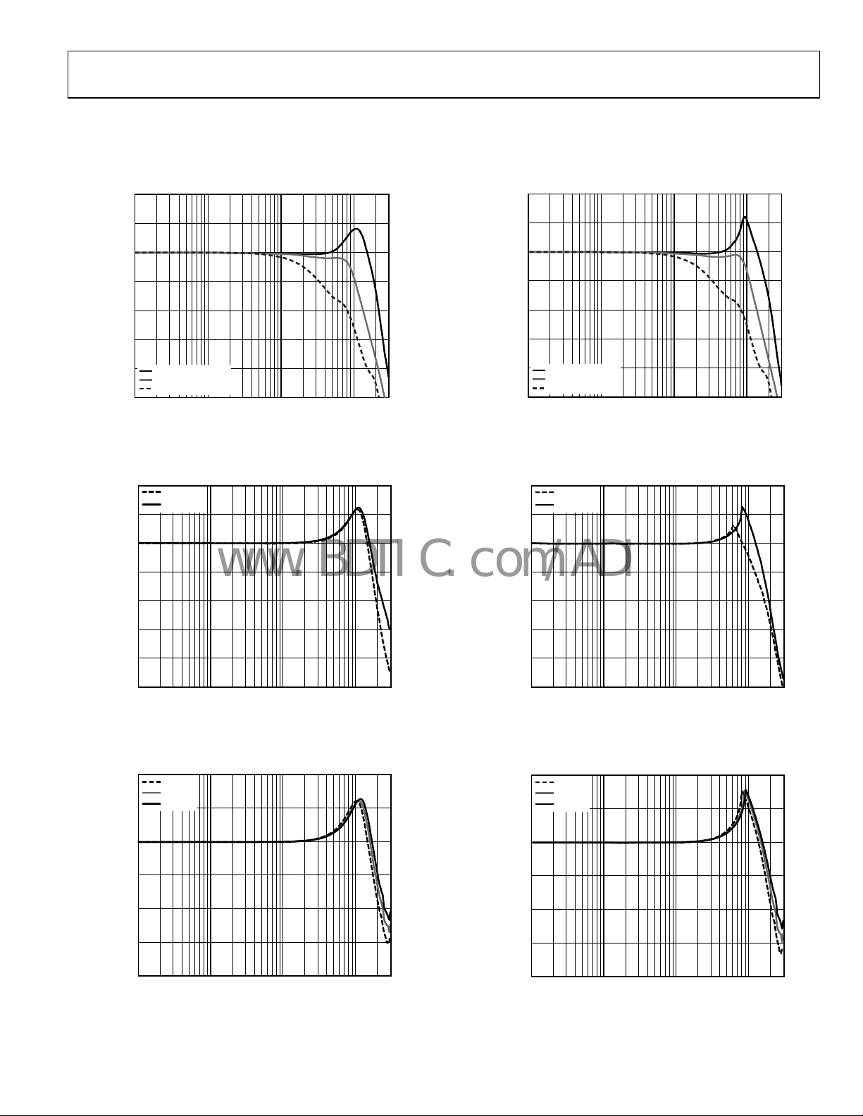
−112 dBc HD2 @ 10 MHz
−84 dBc HD2 @ 70 MHz
−77 dBc HD2 @ 100 MHz
−102 dBc HD3 @ 10 MHz
−91 dBc HD3 @ 70 MHz
−84 dBc HD3 @ 100 MHz
Low input voltage noise: 2.2 nV/√Hz
High speed
−3 dB bandwidth of 1.9 GHz, G = 1
Slew rate: 6000 V/μs, 25% to 75%
Fast overdrive recovery of 1 ns
0.5 mV typical offset voltage
Externally adjustable gain
Differential-to-differential or single-ended-to-differential
oper
ation
Adjustable output common-mode voltage
Single-supply operation: 3.3 V to 5 V
APPLICATIONS
ADC drivers
Single-ended-to-differential converters
IF and baseband gain blocks
Differential buffers
Line drivers
GENERAL DESCRIPTION
The ADA4937 is a low noise, ultralow distortion, high speed
differential amplifier. It is an ideal choice for driving high
performance ADCs with resolutions up to 16 bits from dc to
100 MHz. The adjustable level of the output common mode
allows the ADA4937 to match the input of the ADC. The
internal common-mode feedback loop also provides exceptional
output balance as well as suppression of even-order harmonic
distortion products.
With the ADA4937, differential gain configurations are easily
ealized with a simple external feedback network of four
r
resistors that determine the closed-loop gain of the amplifier.
The ADA4937 is fabricated using Analog Devices, Inc. proprietary
silico
n-germanium (SiGe), complementary bipolar process,
enabling it to achieve very low levels of distortion with an input
voltage noise of only 2.2 nV/√Hz. The low dc offset and excellent
dynamic performance of the ADA4937 make it well suited for a
wide variety of data acquisition and signal processing applications.
Differential ADC Driver
ADA4937-1/ADA4937-2
FUNCTIONAL BLOCK DIAGRAMS
1–FB
2+IN
3–IN
4+FB
1–IN1
2+FB1
3+V
S1
4+V
S1
5–FB2
6+IN2
55
–60
–65
–70
–75
–80
–85
–90
–95
DISTORTION (dBc)
–100
–105
–110
–115
The ADA4937 is available in a Pb-free, 3 mm × 3 mm 16-lead
LFCSP (ADA4937-1, single) or a Pb-free, 4 mm × 4 mm
24-lead LFCSP (ADA4937-2, dual). The pinout has been
optimized to facilitate PCB layout and minimize distortion. The
ADA4937-1 is specified to operate over the −40°C to +105°C
temperature range, and the ADA4937-2 operates over −40°C to
+85°C; both operate at 3.3 V and 5 V supplies.
HD2, VS=5.0V
HD3, VS=5.0V
HD2, VS=3.3V
HD3, VS=3.3V
1 10 100
Figure 3. Harmonic Distortion vs. Frequency
S
S
S
S
–V
–V
–V
–V
14
13
15
16
ADA4937-1
5
6
S
S
+V
+V
12 PD
11 –OUT
10 +OUT
9V
8
7
S
S
+V
+V
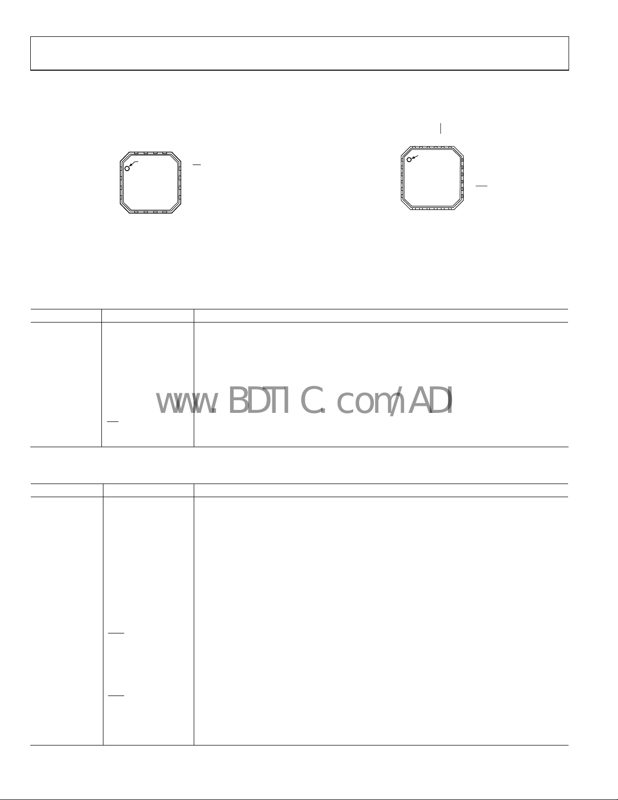
Figure 1. ADA4937-1
S1
S1
–V
–V
–FB1
+IN1
24
ADA4937-2
7
–IN2
–OUT1
PD1
20
19
21
22
23
18 +OUT1
17 V
16 –V
15
14
13 –OUT2
9
8
11
12
10
S2
S2
UT2
+V
+V
OCM2
+FB2
V
+O
Figure 2. ADA4937-2
FREQUENCY (MHz)
–V
PD2
OCM
OCM1
S2
S2
06591-001
06591-002
06591-003
Rev. A
Information furnished by Analog Devices is believed to be accurate and reliable. However, no
responsibility is assumed by Anal og Devices for its use, nor for any infringements of patents or ot her
rights of third parties that may result from its use. Specifications subject to change without notice. No
license is granted by implication or otherwise under any patent or patent rights of Analog Devices.
Trademarks and registered trademarks are the property of their respective owners.
One Technology Way, P.O. Box 9106, Norwood, MA 02062-9106, U.S.A.
Tel: 781.329.4700 www.analog.com
Fax: 781.461.3113 ©2007 Analog Devices, Inc. All rights reserved.

ADA4937-1/ADA4937-2
www.BDTIC.com/ADI
TABLE OF CONTENTS
Features.............................................................................................. 1
Applications....................................................................................... 1
General Description......................................................................... 1
Functional Block Diagrams............................................................. 1
Revision History ...............................................................................2
Specifications..................................................................................... 3
5 V Operation ............................................................................... 3
3.3 V Operation ............................................................................5
Absolute Maximum Ratings............................................................ 7
Thermal Resistance...................................................................... 7
ESD Caution.................................................................................. 7
Pin Configuration and Function Descriptions............................. 8
Typical Performance Characteristics............................................. 9
Test Circuits..................................................................................... 16
Operational Description................................................................ 17
Definition of Terms.................................................................... 17
Theory of Operation ......................................................................18
Analyzing an Application Circuit ............................................ 18
Setting the Closed-Loop Gain .................................................. 18
Estimating the Output Noise Voltage...................................... 18
Impact of Mismatches in the Feedback Networks................. 19
Calculating the Input Impedance for an Application
Circuit.......................................................................................... 19
Input Common-Mode Voltage Range in Single-Supply
Applications ................................................................................ 20
Setting the Output Common-Mode Voltage.......................... 20
Layout, Grounding, and Bypassing.............................................. 22
High Performance ADC Driving................................................. 23
3.3 V Operation.......................................................................... 25
Outline Dimensions....................................................................... 26
Ordering Guide .......................................................................... 26
REVISION HISTORY
11/07—Rev. 0 to Rev. A
Added the ADA4937-2......................................................Universal
Changes to Features.......................................................................... 1
Changes to Specifications................................................................ 3
Changes to Figure 4.......................................................................... 7
Changes to Typical Performance Characteristics......................... 9
Inserted Figure 44........................................................................... 15
Added the Terminating a Single-Ended Input Section .............19
Changes to Table 10 and Table 11 ................................................ 21
Changes to Layout, Grounding, and Bypassing Section ........... 22
Inserted Figure 59, Figure 60, and Figure 61 ..............................22
Updated Outline Dimensions....................................................... 26
Changes to Ordering Guide.......................................................... 26
5/07—Revision 0: Initial Version
Rev. A | Page 2 of 28
ADA4937-1/ADA4937-2
www.BDTIC.com/ADI
SPECIFICATIONS
5 V OPERATION
TA = 25°C, +VS = 5 V, −VS = 0 V, V
All specifications refer to single-ended input and differential outputs, unless otherwise noted.
±DIN to ±OUT Performance
Table 1.
Parameter Conditions Min Typ Max Unit
DYNAMIC PERFORMANCE
−3 dB Small Signal Bandwidth V
Bandwidth for 0.1 dB Flatness V
Large Signal Bandwidth V
Slew Rate V
Overdrive Recovery Time VIN = 0 V to 1.5 V step; G = 3.16 <1 ns
NOISE/HARMONIC PERFORMANCE See Figure 48 for distortion test circuit
Second Harmonic V
V
V
Third Harmonic V
V
V
IMD f1 = 70 MHz; f2 = 70.1 MHz; V
Voltage Noise (RTI) f = 100 kHz 2.2 nV/√Hz
Input Current Noise f = 100 kHz 4 pA/√Hz
Noise Figure G = 4; RT = 136 Ω; RF = 200 Ω; RG = 37 Ω; f = 100 MHz 15 dB
Crosstalk (ADA4937-2) f = 100 MHz −72 dB
INPUT CHARACTERISTICS
Offset Voltage V
T
Input Bias Current −30 −21 −10 μA
T
Input Offset Current −2 +0.5 +2 μA
Input Resistance Differential 6 MΩ
Common mode 3 MΩ
Input Capacitance 1 pF
Input Common-Mode Voltage 0.3 to 3.0 V
CMRR ∆V
OUTPUT CHARACTERISTICS
Output Voltage Swing Maximum ∆V
Linear Output Current >100 mA
Output Balance Error
= +VS/2, RT = 61.9 , RG = RF = 200 , G = 1, R
OCM
= 0.1 V p-p 1900 MHz
OUT, dm
= 0.1 V p-p 200 MHz
OUT, dm
= 2 V p-p 1700 MHz
OUT, dm
= 2 V p-p; 25% to 75% 6000 V/μs
OUT, dm
= 2 V p-p; 10 MHz −112 dBc
OUT, dm
= 2 V p-p; 70 MHz −84 dBc
OUT, dm
= 2 V p-p; 100 MHz −77 dBc
OUT, dm
= 2 V p-p; 10 MHz −102 dBc
OUT, dm
= 2 V p-p; 70 MHz −91 dBc
OUT, dm
= 2 V p-p; 100 MHz −84 dBc
OUT, dm
= 2 V p-p −91 dBc
OUT, dm
∆V
OS, dm
MIN
MIN
OUT, dm
OUT, cm
= V
to T
to T
/2; V
= V
OUT, dm
variation ±1 μV/°C
MAX
variation 0.01 μA/°C
MAX
/∆V
/∆V
DIN+
; ∆V
IN, cm
IN, cm
; single-ended output; RF = RG = 10 kΩ 0.9 4.1 V
OUT
; ∆V
OUT, dm
OUT, dm
= 2.5 V −2.5 ±0.5 +2.5 mV
DIN−
= ±1 V −69 −80 dB
= 1 V; 10 MHz;
see Figure 47 for test circuit
= 1 kΩ, unless otherwise noted.
L, dm
−61 dB
Rev. A | Page 3 of 28

ADA4937-1/ADA4937-2
www.BDTIC.com/ADI
V
to ±OUT Performance
OCM
Table 2.
Parameter Conditions Min Typ Max Unit
V
DYNAMIC PERFORMANCE
OCM
−3 dB Bandwidth 440 MHz
Slew Rate VIN = 1.5 V to 3.5 V; 25% to 75% 1150 V/μs
Input Voltage Noise (RTI) f = 100 kHz 7.5 nV/√Hz
V
INPUT CHARACTERISTICS
OCM
Input Voltage Range 1.2 3.8 V
Input Resistance 8 10 12 kΩ
Input Offset Voltage V
Input Bias Current 0.5 μA
V
CMRR ΔV
OCM
Gain ΔV
POWER SUPPLY
Operating Range 3.0 5.25 V
Quiescent Current per Amplifier 38.0 39.5 42.0 mA
T
Powered down 0.02 0.3 0.5 mA
Power Supply Rejection Ratio ΔV
POWER-DOWN (PD)
PD Input Voltage
Enabled ≥2 V
Turn-Off Time 1 μs
Turn-On Time 200 ns
PD Bias Current per Amplifier
Enabled
Disabled
OPERATING TEMPERATURE RANGE −40 +85 °C
OS, cm
OUT, dm
OUT, cm
MIN
OUT, dm
= V
to T
; V
= V
OUT, cm
DIN+
/ΔV
; ΔV
OCM
OCM
/ΔV
; ΔV
OCM
OCM
variation 17 μA/°C
MAX
= +VS/2 2 7.1 mV
DIN−
= ±1 V −70 −75 dB
= ±1 V 0.97 0.98 1.00 V/V
/ΔVS; ΔVS = 1 V −70 −90 dB
Powered down ≤1 V
PD
PD
= 5 V
= 0 V
10 30 50 μA
−300 −200 −150 μA
Rev. A | Page 4 of 28
ADA4937-1/ADA4937-2
www.BDTIC.com/ADI
3.3 V OPERATION
TA = 25°C, +VS = 3.3 V, −VS = 0 V, V
specifications refer to single-ended input and differential outputs, unless otherwise noted.
±DIN to ±OUT Performance
Table 3.
Parameter Conditions Min Typ Max Unit
DYNAMIC PERFORMANCE
−3 dB Small Signal Bandwidth V
Bandwidth for 0.1 dB Flatness V
Large Signal Bandwidth V
Slew Rate V
Overdrive Recovery Time VIN = 0 V to 1.0 V step; G = 3.16 <1 ns
NOISE/HARMONIC PERFORMANCE See Figure 48 for distortion test circuit
Second Harmonic V
V
V
Third Harmonic V
V
V
IMD f1 = 70 MHz; f2 = 70.1 MHz; V
Voltage Noise (RTI) f = 100 kHz 2.2 nV/√Hz
Input Current Noise f = 100 kHz 4 pA/√Hz
Noise Figure G = 4; RT = 136 Ω; RF = 200 Ω; RG = 37 Ω; f = 100 MHz 15 dB
Crosstalk (ADA4937-2) f = 100 MHz −72 dB
INPUT CHARACTERISTICS
Offset Voltage V
T
Input Bias Current −50 −20 −10 μA
T
Input Resistance Differential 6 MΩ
Common mode 3 MΩ
Input Capacitance 1 pF
Input Common-Mode Voltage 0.3 to 1.2 V
CMRR ∆V
OUTPUT CHARACTERISTICS
Output Voltage Swing Maximum ∆V
Linear Output Current 95 mA
Output Balance Error
= +VS/2, RT = 61.9 , RG = RF = 200 , G = 1, R
OCM
= 0.1 V p-p 1800 MHz
OUT, dm
= 0.1 V p-p 200 MHz
OUT, dm
= 2 V p-p 1300 MHz
OUT, dm
= 2 V p-p; 25% to 75% 4000 V/μs
OUT, dm
= 2 V p-p; 10 MHz −113 dBc
OUT, dm
= 2 V p-p; 70 MHz −85 dBc
OUT, dm
= 2 V p-p; 100 MHz −77 dBc
OUT, dm
= 2 V p-p; 10 MHz −95 dBc
OUT, dm
= 2 V p-p; 70 MHz −77 dBc
OUT, dm
= 2 V p-p; 100 MHz −71 dBc
OUT, dm
= 2 V p-p −87 dBc
OUT, dm
∆V
OS, dm
MIN
MIN
OUT, dm
OUT, cm
= V
to T
to T
/2; V
= V
OUT, dm
variation ±1 μV/°C
MAX
variation 0.01 μA/°C
MAX
/∆V
/∆V
DIN+
; ∆V
IN, cm
IN, cm
; single-ended output; RF = RG = 10 kΩ 0.8 2.5 V
OUT
; ∆V
OUT, dm
OUT, dm
= +VS/2 −2.5 ±0.5 +2.5 mV
DIN−
= ±1 V −67 −80 dB
= 1 V; f = 10 MHz;
see Figure 47 for test circuit
= 1 kΩ, unless otherwise noted. All
L, dm
−61 dB
Rev. A | Page 5 of 28
ADA4937-1/ADA4937-2
www.BDTIC.com/ADI
V
to ±OUT Performance
OCM
Table 4.
Parameter Conditions Min Typ Max Unit
V
DYNAMIC PERFORMANCE
OCM
−3 dB Bandwidth 440 MHz
Slew Rate VIN = 0.9 V to 2.4 V; 25% to 75% 900 V/μs
Input Voltage Noise (RTI) f = 100 kHz 7.5 nV/√Hz
V
INPUT CHARACTERISTICS
OCM
Input Voltage Range 1.2 2.1 V
Input Resistance 10 kΩ
Input Offset Voltage V
Input Bias Current 0.5 μA
V
CMRR ∆V
OCM
Gain ∆V
POWER SUPPLY
Operating Range 3.0 5.25 V
Quiescent Current per Amplifier 36 38 40 mA
T
Powered down 0.02 0.2 0.5 mA
Power Supply Rejection Ratio ∆V
POWER-DOWN (PD)
PD Input Voltage
Enabled ≥2 V
Turn-Off Time 1 μs
Turn-On Time 200 ns
PD Bias Current per Amplifier
Enabled
Disabled
OPERATING TEMPERATURE RANGE −40 +105 °C
OS, cm
OUT, dm
OUT, cm
MIN
OUT, dm
= V
to T
; V
= V
OUT, cm
DIN+
/∆V
; ∆V
OCM
OCM
/∆V
; ∆V
OCM
OCM
variation 17 μA/°C
MAX
= 1.67 V 2 7.1 mV
DIN−
= ±1 V −70 −75 dB
= ±1 V 0.97 0.98 1.00 V/V
/∆VS; ∆VS = 1 V −70 −90 dB
Powered down ≤1 V
PD
PD
= 3.3 V
= 0 V
10 20 30 μA
−200 −120 −100 μA
Rev. A | Page 6 of 28
ADA4937-1/ADA4937-2
www.BDTIC.com/ADI
ABSOLUTE MAXIMUM RATINGS
Table 5.
Parameter Rating
Supply Voltage 5.5 V
Power Dissipation See Figure 4
Storage Temperature Range −65°C to +125°C
Operating Temperature Range
ADA4937-1 −40°C to +105°C
ADA4937-2 −40°C to +85°C
Lead Temperature (Soldering, 10 sec) 300°C
Junction Temperature 150°C
Stresses above those listed under Absolute Maximum Ratings
may cause permanent damage to the device. This is a stress
rating only; functional operation of the device at these or any
other conditions above those indicated in the operational
section of this specification is not implied. Exposure to absolute
maximum rating conditions for extended periods may affect
device reliability.
THERMAL RESISTANCE
θJA is specified for the device (including exposed pad) soldered
to a high thermal conductivity 2s2p circuit board, as described
in EIA/JESD 51-7.
Table 6. Thermal Resistance
Package Type θJA Unit
16-Lead LFCSP (Exposed Pad) 95 °C/W
24-Lead LFCSP (Exposed Pad) 67 °C/W
Maximum Power Dissipation
The maximum safe power dissipation in the ADA4937 package
is limited by the associated rise in junction temperature (T
the die. At approximately 150°C, which is the glass transition
temperature, the plastic changes its properties. Even temporarily
exceeding this temperature limit can change the stresses that the
package exerts on the die, permanently shifting the parametric
performance of the ADA4937. Exceeding a junction temperature
of 150°C for an extended period can result in changes in the
silicon devices, potentially causing failure.
) on
J
The power dissipated in the package (P
quiescent power dissipation and the power dissipated in the
package due to the load drive. The quiescent power is the voltage
between the supply pins (V
) times the quiescent current (IS).
S
The power dissipated due to the load drive depends upon the
particular application. The power due to load drive is calculated
by multiplying the load current by the associated voltage drop
across the device. RMS voltages and currents must be used in
these calculations.
Airflow increases heat dissipation, effectively reducing θ
addition, more metal directly in contact with the package
leads/exposed pad from metal traces, through holes, ground,
and power planes reduces θ
.
JA
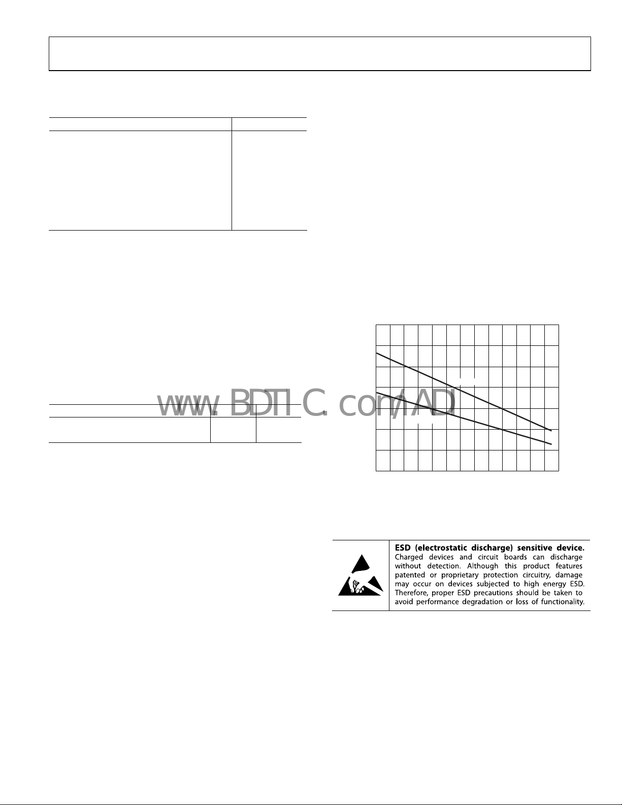
Figure 4 shows the maximum safe power dissipation in the
ackage vs. the ambient temperature for the single 16-lead
p
LFCSP (95°C/W) and the dual 24-lead LFCSP (67°C/W) on a
JEDEC standard 4-layer board.
3.5
3.0
2.5
2.0
1.5
1.0
MAXIMUM POWER DISSIPATION (W)
0.5
0
–40 90
Figure 4. Maximum Power Dissipation vs. Temperature for a 4-Layer Board
ADA4937-1
–30–20–100 1020304050607080
ADA4937-2
AMBIENT TEMPERATURE (°C)
ESD CAUTION
) is the sum of the
D
JA
. In
06591-004
Rev. A | Page 7 of 28
ADA4937-1/ADA4937-2
+
–
www.BDTIC.com/ADI
PIN CONFIGURATION AND FUNCTION DESCRIPTIONS
S
S
S
1–FB
2+IN
ADA4937-1
3–IN
(Not to Scale)
4+FB
–V
–V
15
16
PIN 1
INDICATO R
TOP VIEW
5
6
S
S
+V
+V
S
–V
–V
14
13
–IN1
12 PD
11 –OUT
10 +OUT
9V
OCM
8
7
S
S
+V
+V
06591-005
FB1
+V
+V
FB2
+IN2
S1
S1
1
2
3
ADA4937-2
4
5
6
+IN1
24
PIN 1
INDICATOR
TOP VIEW
(Not to Scale)
7
–IN2
–OUT1
–VS1–VS1–FB1
PD1
20
19
21
22
23
18
+OUT1
17
V
OCM1
–V
16
S2
–V
15
S2
14
PD2
13
–OUT2
9
8
11
12
10
S2
S2
CM2
+V
+V
O
+FB2
V
+OUT2
06591-006
Figure 5. ADA4937-1 Pin Configuration
Figure 6. ADA4937-2 Pin Configuration
Table 7. ADA4937-1 Pin Function Descriptions
Pin No. Mnemonic Description
1 −FB Negative Output for Feedback Component Connection.
2 +IN Positive Input Summing Node.
3 −IN Negative Input Summing Node.
4 +FB Positive Output for Feedback Component Connection.
5 to 8 +VS Positive Supply Voltage.
9 V
Output Common-Mode Voltage.
OCM
10 +OUT Positive Output for Load Connection.
11 −OUT Negative Output for Load Connection.
12
PD
Power-Down Pin.
13 to 16 −VS Negative Supply Voltage.
Table 8. ADA4937-2 Pin Function Descriptions
Pin No. Mnemonic Description
1 −IN1 Negative Input Summing Node 1.
2 +FB1 Positive Output Feedback Pin 1.
3, 4 +VS1 Positive Supply Voltage 1.
5 −FB2 Negative Output Feedback Pin 2.
6 +IN2 Positive Input Summing Node 2.
7 −IN2 Negative Input Summing Node 2.
8 +FB2 Positive Output Feedback Pin 2.
9, 10 +VS2 Positive Supply Voltage 2.
11 V
Output Common-Mode Voltage 2.
OCM2
12 +OUT2 Positive Output 2.
13 −OUT2 Negative Output 2.
14
PD2
Power-Down Pin 2.
15, 16 −VS2 Negative Supply Voltage 2.
17 V
Output Common-Mode Voltage 1.
OCM1
18 +OUT1 Positive Output 1.
19 −OUT1 Negative Output 1.
20
PD1
Power-Down Pin 1.
21, 22 −VS1 Negative Supply Voltage 1.
23 −FB1 Negative Output Feedback Pin 1.
24 +IN1 Positive Input Summing Node 1.
Rev. A | Page 8 of 28
ADA4937-1/ADA4937-2
www.BDTIC.com/ADI
TYPICAL PERFORMANCE CHARACTERISTICS
TA = 25°C, +VS = 5 V, −VS = 0 V, V
noted. Refer to Figure 46 for test setup.
6
OUT, dm
= 2 V p-p, V
= +VS /2, RT = 61.9 , RG = RF = 200 , G = 1, R
OCM
6
= 1 kΩ, unless otherwise
L, dm
3
0
–3
–6
–9
–12
NORMALIZ ED CLOSED-L OOP GAI N (dB)
G = +1, RF = 200Ω
G = +2, R
= 402Ω
F
G = +5, R
= 402Ω
–15
1 10 100 1000
F
FREQUENCY (MHz )
Figure 7. Small Signal Frequency Response for Various Gains,
V
= 100 mV p-p
OUT, dm
6
VS = 3.3V
VS = 5.0V
3
0
–3
–6
–9
CLOSED-LOOP GAIN (dB)
–12
3
0
–3
–6
–9
–12
NORMALIZ ED CLOSED- LOOP G AIN (dB)
6591-075
G = +1, RF = 200Ω
G = +2, R
= 402Ω
F
G = +5, R
= 402Ω
–15
1 10 100 1000
F
FREQUENCY (MHz)
06591-076
Figure 10. Large Signal Frequency Response for Various Gains
6
VS = 3.3V
VS = 5.0V
3
0
–3
–6
–9
CLOSED-LOOP GAIN (dB)
–12
–15
1 10 100 1000
FREQUENCY (MHz)
Figure 8. Small Signal Frequency Response for Various Supplies,
= 100 mV p-p
V
OUT, dm
6
+105°C
+25°C
–40°C
3
0
–3
–6
CLOSED-LOOP GAIN (dB)
–9
–12
1 10 100 1000
FREQUENCY (MHz)
Figure 9. Small Signal Frequency Response for Various Temperatures,
= 100 mV p-p
V
OUT, dm
06591-008
06591-009
Rev. A | Page 9 of 28
–15
1 10 100 1000
FREQUENCY (MHz)
Figure 11. Large Signal Frequency Response for Various Supplies
6
+105°C
+25°C
–40°C
3
0
–3
–6
CLOSED-LOOP GAIN (dB)
–9
–12
1 10 100 1000
FREQUENCY (MHz)
Figure 12. Large Signal Frequency Response for Various Temperatures
06591-011
06591-012

ADA4937-1/ADA4937-2
www.BDTIC.com/ADI
6
RL = 1kΩ
RL = 100Ω
RL = 200Ω
3
6
RL = 1kΩ
RL = 100Ω
RL = 200Ω
3
0
–3
CLOSED-LOOP GAIN (dB)
–6
–9
1 10 100 1000
FREQUENCY (MHz)
Figure 13. Small Signal Frequency Response for Various Loads,
= 100 mV p-p
V
OUT, dm
6
3
0
–3
–6
–9
–12
NORMALIZ ED CLOSED- LOOP G AIN (dB)
VS = 3.3V, G = +1, RF = 200Ω
= 3.3V, G = +2, RF = 402Ω
V
S
= 3.3V, G = +5, RF = 402Ω
V
–15
S
1 10 100 1000
FREQUENCY (M Hz)
Figure 14. Small Signal Frequency Response for Various Gains,
= 3.3 V and V
V
S
= 100 mV p-p
OUT, dm
0
–3
CLOSED-LOOP GAIN (dB)
–6
–9
1 10 100 1000
06591-013
FREQUENCY (MHz)
06591-016
Figure 16. Large Signal Frequency Response for Various Loads
6
3
0
–3
–6
–9
–12
NORMALIZ ED CLOSED- LOOP G AIN (dB)
06591-077
Figure 17. Large Signal Frequency Response for Various Gains, V
VS = 3.3V, G = +1, RF = 200Ω
V
= 3.3V, G = +2, RF = 402Ω
S
V
= 3.3V, G = +5, RF = 402Ω
S
–15
1 10 100 1000
FREQUENCY (MHz )
= 3.3 V
S
06591-079
6
3
0
–3
–6
–9
–12
NORMALIZ ED CLOSED- LOOP G AIN (dB)
G = +1, RF = 348Ω
G = +2, R
= 348Ω
F
G = +5, R
= 348Ω
–15
1 10 100 1000
F
FREQUENCY (M Hz)
06591-078
Figure 15. Small Signal Frequency Response for Various Gains,
= 100 mV p-p, RF = 348 Ω
V
OUT, dm
Rev. A | Page 10 of 28
6
3
0
–3
–6
–9
–12
NORMALIZ ED CLOSED- LOOP G AIN (dB)
G = +1, RF = 348Ω
G = +2, R
= 348Ω
F
G = +5, R
= 348Ω
–15
1 10 100 1000
F
FREQUENCY (MHz)
Figure 18. Large Signal Frequency Response for Various Gains, R
= 348 Ω
F
6591-080

ADA4937-1/ADA4937-2
–
–
–
–
www.BDTIC.com/ADI
3
V
= 1.0V
OCM
V
= 2.5V
OCM
V
= 3.9V
0
–3
OCM
–60
–70
–80
50
HD2, G = +1, RF = 200Ω
HD3, G = +1, RF = 200Ω
HD2, G = +2, RF = 402Ω
HD3, G = +2, RF = 402Ω
–6
CLOSED-LOOP GAIN (dB)
OCM
–9
V
–12
1 10 100 1000
FREQUENCY (M Hz)
Figure 19. Small Signal Frequency Response
arious V
for V
1.5
RL = 1kΩ, ADA4937-1
1.4
R
= 100Ω, ADA4937-1
1.3
1.2
1.1
1.0
0.9
0.8
0.7
0.6
0.5
0.4
GAIN (dB)
0.3
0.2
0.1
–0.1
–0.2
–0.3
–0.4
–0.5
L
R
= 1kΩ, ADA4937-2
L
R
= 100Ω, ADA4937-2
L
0
1 10 100 1000
FREQUENCY (MHz)
OCM
Figure 20. 0.1 dB Flatness Response for Various Loads
–90
DISTORTION (dBc)
–100
–110
–120
1 10 100
06591-019
FREQUENCY (MHz)
06591-022
Figure 22. Harmonic Distortion vs. Frequency and Gain
50
–60
–70
–80
–90
DISTORTION (dBc)
–100
–110
–120
06591-020
HD2, RL = 1kΩ
HD3, RL = 1kΩ
HD2, RL = 200Ω
HD3, RL = 200Ω
1 10 100
FREQUENCY (MHz)
06591-023
Figure 23. Harmonic Distortion vs. Frequency and Load
55
–60
–65
–70
–75
–80
–85
–90
–95
DISTORTION (dBc)
–100
–105
–110
–115
HD2, VS = 5.0V
HD3, VS = 5.0V
HD2, VS = 3.3V
HD3, VS = 3.3V
1 10 100
FREQUENCY (MHz)
06591-021
Figure 21. Harmonic Distortion vs. Frequency and Supply Voltage
Rev. A | Page 11 of 28
50
–60
–70
–80
–90
–100
DISTORTION (dBc)
–110
–120
–130
–1 76543210
HD2, VS = 3.3V
HD3, VS = 3.3V
HD2, VS = 5.0V
HD3, VS = 5.0V
Figure 24. Harmonic Distortion vs. V
V
(V)
OUT
and Supply Voltage
OUT
06591-024

ADA4937-1/ADA4937-2
–
–
–
–
–
www.BDTIC.com/ADI
30
–40
–50
–60
–70
–80
–90
DISTORTION (dBc)
–100
–110
–120
1.0 4.03.53.02.52.01.5
HD2, f = 10MHz
HD3, f = 10MHz
HD2, f = 75MHz
HD3, f = 75MHz
Figure 25. Harmonic Distortion vs. V
V
(V)
OCM
and Frequency
OCM
06591-025
0
–20
–40
–60
–80
DISTORTION (dBc)
–100
–120
69.4 69.6 70.670.470.270.069.8
Figure 28. 70 MHz Intermodulation Distortion
FREQUENCY (M Hz)
06591-028
40
–50
–60
–70
–80
DISTORTION (dBc)
–90
–100
1.1 2.01.91.81.71.61.51.41.31.2
Figure 26. Harmonic Distortion vs. V
DISTORTION (dBc)
50
–60
–70
–80
–90
–100
–110
–120
–130
HD2, 1V p-p
HD3, 1V p-p
HD2, 2V p-p
HD3, 2V p-p
1 10 100
HD2, f = 30MHz
HD3, f = 30MHz
HD2, f = 75MHz
HD3, f = 75MHz
V
(V)
OCM
and Frequency, VS = 3.3 V
OCM
FREQUENCY (MHz)
Figure 27. Harmonic Distortion vs. Frequency and V
, VS = 3.3 V
OUT
30
RL = 200Ω
–40
–50
CMRR (dB)
–60
–70
1 100010010
06591-026
FREQUENCY (MHz)
06591-029
Figure 29. CMRR vs. Frequ ency
10
RL = 200Ω
–20
–30
–40
OUTPUT BALANCE (dB)
–50
–60
1 10 100 1000
06591-027
FREQUENCY (MHz)
6591-068
Figure 30. Output Balance vs. Frequency
Rev. A | Page 12 of 28

ADA4937-1/ADA4937-2
–
–
www.BDTIC.com/ADI
30
V
PSRR, VS = 3.3V
OUT, dm
V
PSRR, VS = 5.0V
OUT, dm
1 10 100 1000
Figure 31. PSRR v s. Frequency, R
FREQUENCY (M Hz)
= 200 Ω
L
PSRR (dB)
–40
–50
–60
–70
–80
–90
–100
06591-031
28
G = +1
G = +2
26
G = +4
24
22
20
18
16
NOISE FI GURE (dB)
14
12
10
10 100
FREQUENCY (MHz)
Figure 34. Noise Figure vs. Frequ ency
06591-034
0
S11
–5
–10
–15
–20
–25
–30
–35
–40
–45
S-PARAMETERS (dB)
–50
–55
–60
–65
S22
1 10 100 1000
FREQUENCY (MHz)
Figure 32. Return Loss (S11, S22) vs. Frequency
55
–60
–65
–70
–75
–80
–85
–90
–95
DISTORTION (dBc)
–100
–105
–110
–115
SFDR, RL = 1kΩ
SFDR, RL = 200Ω
1 10 100
FREQUENCY (MHz)
Figure 33. Spurious-Free Dynamic Range vs. Frequency and Load
5
4
3
2
1
0
–1
VOLTAGE (V)
–2
–3
–4
–5
06591-032
VIN × 3.16
V
OUT, dm
TIME (4ns/DIV)
06591-069
Figure 35. Overdrive Recovery Time (Pulse Input)
5
4
3
2
1
0
–1
SIGNAL LEVEL (V)
–2
–3
–4
–5
0 100 200 300 400 500 600
06591-033
V
× 3
IN
V
OUT, dm
TIME (ns)
+VS = +2.5V
= –2.5V
–V
S
06591-070
Figure 36. Overdrive Amplitude Characteristics ( Triangle Wave Input)
Rev. A | Page 13 of 28

ADA4937-1/ADA4937-2
www.BDTIC.com/ADI
60
55
50
45
40
35
30
25
20
SUPPLY CURRENT (mA)
15
10
5
0
1.0 2.01.91.81.71.61. 51.3 1.41.21.1
Figure 37. Supply Current vs.
+25°C
0°C
–40°C
POWER-DOW N VOLTAGE (V)
PD
+55°C
for Various Temperatures
+105°C
06591-037
60
55
50
45
40
35
30
25
20
SUPPLY CURRENT (mA)
15
10
5
0
1.0 2.01.91.81.71.61. 51.3 1.41.21.1
–40°C
POWER-DOW N VOLTAGE (V)
Figure 40. Supply Current vs.
+25°C
+105°C
0°C
PD
for Various Temperatures, VS = 3.3 V
+55°C
06591-040
VOLTAGE (V)
0.20
0.15
0.10
0.05
–0.05
–0.10
–0.15
–0.20
2.60
2.58
2.56
2.54
2.52
2.50
2.48
2.46
OUTPUT VOLTAGE (V)
2.44
2.42
2.40
0
TIME (1ns/DIV)
Figure 38. Small Signal Pulse Response
TIME (2ns/DIV)
Figure 39. Small Signal V
Pulse Response
OCM
+VS = +2.5V
= –2.5V
–V
S
= 0V
V
OCM
VS = +5V
G = 1
R
= 1kΩ
L, dm
3.5
3.0
2.5
2.0
1.5
1.0
0.5
0
–0.5
VOLTAGE (V)
–1.0
–1.5
–2.0
–2.5
–3.0
6591-071
–3.5
V
= 4V p-p
OUT, dm
V
= 2V p-p
OUT, dm
TIME (1ns/DIV)
+VS = +2.5V
–V
= –2.5V
S
V
= 0V
OCM
06591-074
Figure 41. Large Signal Pulse Response
4.00
3.75
3.50
3.25
3.00
2.75
2.50
2.25
2.00
OUTPUT VOLTAGE (V)
1.75
1.50
1.25
06591-072
1.00
Figure 42. Large Signal V
TIME (2ns/DIV)
Pulse Response
OCM
VS = +5V
G = 1
R
L, dm
= 1kΩ
06591-073
Rev. A | Page 14 of 28

ADA4937-1/ADA4937-2
–
www.BDTIC.com/ADI
2.4
2.2
2.0
1.8
1.6
1.4
1.2
1.0
VOLTAGE (V)
0.8
0.6
0.4
0.2
0
Figure 43.
PD INPUT
SINGLE O UTPUT
TIME (150ns/DIV)
PD
Response vs. Time
06591-043
100
10
INPUT VOLTAGE NOISE (nV/ Hz)
1
10 10M1M100k10k1k100
FREQUENCY (Hz)
Figure 45. Voltage Spectral Noise Density, RTI
06591-045
CROSSTALK (d B)
–50
–60
–70
–80
–90
–100
–110
–120
–130
–140
40
INPUT2, OUTPUT1
INPUT1, OUTPUT2
10.3 10 100 10 00
FREQUENCY (MHz)
06591-044
Figure 44. Crosstalk vs. Frequency for ADA4937-2
Rev. A | Page 15 of 28

ADA4937-1/ADA4937-2
www.BDTIC.com/ADI
TEST CIRCUITS
200Ω
5V
200Ω50Ω
V
IN
61.9Ω
V
OCM
200Ω
27.5Ω
ADA4937
200Ω
1kΩ
06591-046
Figure 46. Equivalent Basic Test Circuit
200Ω
5V
200Ω50Ω
V
IN
61.9Ω
V
OCM
200Ω
27.5Ω
ADA4937
200Ω
50Ω
50Ω
06591-047
Figure 47. Test Circuit for Output Balance
200Ω
5V
FILTER
V
IN
61.9Ω
200Ω50Ω
V
OCM
200Ω
27.5Ω
ADA4937
200Ω
0.1µF
0.1µF
412Ω
412Ω
FILTER
06591-048
Figure 48. Test Circuit for Distortion Measurements
Rev. A | Page 16 of 28

ADA4937-1/ADA4937-2
–
V
www.BDTIC.com/ADI
OPERATIONAL DESCRIPTION
DEFINITION OF TERMS
FB
R
F
R
G
+D
OCM
–D
+FB
IN
IN
+IN
ADA4937
–IN
R
G
R
F
Figure 49. Circuit Definitions
Differential Voltage
Differential voltage refers to the difference between two node
voltages. For example, the output differential voltage (or
equivalently, output differential-mode voltage) is defined as
V
where V
OUT, dm
+OUT
= (V
and V
− V
+OUT
−OUT
refer to the voltages at the +OUT and
−OUT
−OUT terminals with respect to a common reference.
–OUT
V
R
OUT, dm
L, dm
+OUT
06591-049
)
Common-Mode Voltage
Common-mode voltage refers to the average of two node
voltages. The output common-mode voltage is defined as
V
OUT, cm
= (V
+OUT
+ V
−OUT
)/2
Balance
Output balance is a measure of how close the differential signals
are to being equal in amplitude and opposite in phase. Output
balance is most easily determined by placing a well-matched
resistor divider between the differential voltage nodes and
comparing the magnitude of the signal at the divider’s midpoint
with the magnitude of the differential signal (see
th
is definition, output balance is the magnitude of the output
Figure 47). By
common-mode voltage divided by the magnitude of the output
differential mode voltage.
V
cmOUT
,
=
ErrorBalanceOutput
V
dmOUT
,
Rev. A | Page 17 of 28

ADA4937-1/ADA4937-2
V
V
www.BDTIC.com/ADI
THEORY OF OPERATION
The ADA4937 differs from conventional op amps in that it has
two outputs whose voltages move in opposite directions. Like
an op amp, it relies on open-loop gain and negative feedback to
force these outputs to the desired voltages. The ADA4937
behaves much like a standard voltage feedback op amp, which
makes it easier to perform single-ended-to-differential
conversions, common-mode level shifting, and amplifications
of differential signals. Also like an op amp, the ADA4937 has
high input impedance and low output impedance.
Two feedback loops are employed to control the differential and
mmon-mode output voltages. The differential feedback, set
co
with external resistors, controls only the differential output
voltage. The common-mode feedback controls only the commonmode output voltage. This architecture makes it easy to set the
output common-mode level to any arbitrary value. It is forced,
by internal common-mode feedback, to be equal to the voltage
applied to the V
input, without affecting the differential
OCM
output voltage.
The ADA4937 architecture results in outputs that are highly
b
alanced over a wide frequency range without requiring tightly
matched external components. The common-mode feedback
loop forces the signal component of the output commonmode voltage to zero. This results in nearly perfectly balanced
differential outputs that are identical in amplitude and are
exactly 180° apart in phase.
ANALYZING AN APPLICATION CIRCUIT
The ADA4937 uses open-loop gain and negative feedback to
force its differential and common-mode output voltages in such
a way as to minimize the differential and common-mode error
voltages. The differential error voltage is defined as the voltage
between the differential inputs labeled +IN and −IN (see
Figure 49). For most purposes, this voltage can be assumed to
e zero. Similarly, the difference between the actual output
b
common-mode voltage and the voltage applied to V
be assumed to be zero. Starting from these two assumptions,
any application circuit can be analyzed.
can also
OCM
SETTING THE CLOSED-LOOP GAIN
The differential-mode gain of the circuit in Figure 49 can be
determined by
V
V
This assumes that the input resistors (R
(R
) on each side are equal.
F
R
dmOUT
,
dmIN
,
F
=
R
G
) and feedback resistors
G
ESTIMATING THE OUTPUT NOISE VOLTAGE
The differential output noise of the ADA4937 can be estimated
using the noise model in Figure 50. The input-referred noise
tage density, v
vol
noise currents, i
ground. The noise currents are assumed to be equal and produce
a voltage across the parallel combination of the gain and feedback
resistances. v
Each of the four resistors contributes (4kTR
rizes the input noise sources, the multiplication factors, and the
output-referred noise density terms.
, is modeled as a differential input, and the
nIN
and i
nIN−
is the noise voltage density at the V
nCM
nRG1
R
G1
i
nIN+
i
nIN–
R
G2
V
nRG2
Figure 50. ADA4937 Noise Model
, appear between each input and
nIN+
1/2
)
x
nRF1
R
F1
+
V
nIN
R
ADA4937
V
F2
V
OCM
nRF2
V
nOD
pin.
OCM
. Table 9 summa-
V
nCM
06591-050
Table 9. Output Noise Voltage Den
sity Calculations
Input Noise
V
Input Noise Contribution Input Noise Term
Differential Input v
Inverting Input i
Noninverting Input i
V
Input v
OCM
Gain Resistor RG1 v
Gain Resistor RG2 v
Feedback Resistor RF1 v
Feedback Resistor RF2 v
v
nIN
i
nIN−
i
nIN+
v
nCM
(4kTRG1)
nRG1
(4kTRG2)
nRG2
(4kTRF1)
nRF1
(4kTRF2)
nRF2
oltage Density
G
nIN
× (RG2||RF2) GN v
nIN−
× (RG1||RF1) GN v
nIN+
G
nCM
1/2
G
1/2
G
1/2
1 v
1/2
1 v
Rev. A | Page 18 of 28
Output
Multiplication Factor
v
N
− β2) v
N(β1
(1 − β2) v
N
(1 − β1) v
N
Output Noise
Voltage Density Term
= GN(v
nO1
= GN[i
nO2
= GN[i
nO3
= GN(β1 − β2)(v
nO4
= GN(1 − β2)(4kTRG1)
nO5
= GN(1 − β1)(4kTRG2)
nO6
= (4kTRF1)
nO7
= (4kTRF2)
nO8
)
nIN
× (RG2||RF2)]
nIN−
× (RG1||RF1)]
nIN+
1/2
1/2
nCM
)
1/2
1/2

ADA4937-1/ADA4937-2
www.BDTIC.com/ADI
Similar to the case of a conventional op amp, the output noise
voltage densities can be estimated by multiplying the inputreferred terms at +IN and −IN by the appropriate output factor,
where:
2
=
N
β+=
1
When R
(
F1
is the circuit noise gain.
)
ββG+
21
R
G1
and
RR
F1/RG1
G1
β+=
= RF2/RG2, then β1 = β2 = β, and the noise gain
R
G2
2
F2
are the feedback factors.
RR
G2
becomes
R
1
G +== 1
N
β
Note that the output noise from V
The total differential output noise density, v
F
R
G
goes to zero in this case.
OCM
, is the root-sum-
nOD
square of the individual output noise terms.
8
2
=
vv
∑
nOinOD
1i
=
IMPACT OF MISMATCHES IN THE FEEDBACK NETWORKS
As previously mentioned, even if the external feedback networks
) are mismatched, the internal common-mode feedback
(R
F/RG
loop still forces the outputs to remain balanced. The amplitudes
of the signals at each output remain equal and 180° out of phase.
The input-to-output differential mode gain varies proportionately
to the feedback mismatch, but the output balance is unaffected.
As well as causing a noise contribution from V
OCM
, ratio
matching errors in the external resistors result in a degradation
of the ability of the circuit to reject input common-mode signals,
much the same as for a four-resistor difference amplifier made
from a conventional op amp.
In addition, if the dc levels of the input and output common-
ode voltages are different, matching errors result in a small
m
differential-mode output offset voltage. When G = 1, with a
ground referenced input signal and the output common-mode
level set to 2.5 V, an output offset of as much as 25 mV (1% of
the difference in common-mode levels) can result if 1% tolerance
resistors are used. Resistors of 1% tolerance result in a worstcase input CMRR of about 40 dB, a worst-case differentialmode output offset of 25 mV due to 2.5 V level-shift, and no
significant degradation in output balance error.
CALCULATING THE INPUT IMPEDANCE FOR AN APPLICATION CIRCUIT
The effective input impedance of a circuit depends on whether
the amplifier is being driven by a single-ended or differential
signal source. For balanced differential input signals, as shown
in Figure 51, the input impedance (R
(+D
and −DIN) is simply R
IN
IN, dm
= 2 × RG.
) between the inputs
IN, dm
Rev. A | Page 19 of 28
R
F
ADA4937
+V
+IN
OCM
–IN
S
V
OUT, dm
R
F
06591-051
R
+D
–D
Figure 51. ADA4937 Configured for Balanced (Differential) Inputs
G
IN
IN
V
R
G
For an unbalanced, single-ended input signal (see Figure 52),
the input impedance is
F
+×
V
OCM
RR
F
⎞
⎟
⎟
⎟
⎟
⎟
⎠
R
F
+V
S
ADA4937
R
F
V
OUT, dm
06591-052
⎛
⎜
R
Figure 52. ADA4937 Configured for Unbalanced (Single-Ended) Input
⎜
=
cmIN
,
⎜
⎜
⎜
⎝
R
S
R
G
1
R
R
−
()
2
G
R
G
T
R
G
R
R
T
S
The input impedance of the circuit is effectively higher than it
would be for a conventional op amp connected as an inverter
because a fraction of the differential output voltage appears at
the inputs as a common-mode signal, partially bootstrapping
the voltage across the input resistor R
.
G
Terminating a Single-Ended Input
This section deals with how to properly terminate a singleended input to the ADA4937. Using a simple example with an
input source of 2 V and a source resistor of 50 Ω, four simple
steps must be followed.
1.
The input impedance must be calculated using the formula
F
+×
R
G
OCM
R
G
RR
)(2
F
⎞
⎛
⎟
⎜
⎟
⎜
=
⎟
⎜
1
⎟
⎜
⎟
⎝
⎠
R
F
200Ω
+V
ADA4937
–V
R
F
200Ω
⎞
+×
RLV
⎟
⎟
=
⎟
⎟
)200200(2
⎠
O
06591-081
200
−
S
S
200
⎛
⎜
⎜
R
=
IN
⎜
1
⎜
⎜
⎝
R
50Ω
V
S
2V
R
G
R
267Ω
R
G
IN
200Ω
V
200Ω
−
S
Figure 53. Single-Ended Input Impedance RIN
267

ADA4937-1/ADA4937-2
www.BDTIC.com/ADI
2. In order for the source termination to be 50 Ω, the termi-
nation resistor (R
which makes R
50Ω
R
S
50Ω
V
S
2V
Figure 54. Adding Termination Resistor R
) is calculated using RT||RIN = 50 Ω,
T
equal to 61.9 Ω.
T
R
F
200Ω
+V
S
R
G
200Ω
R
T
61.9Ω
V
OCM
R
200Ω
ADA4937
G
–V
S
R
F
200Ω
T
RLV
O
3. To compensate for the imbalance of the gain resistors,
a correction resistor (R
inverting input gain resistor R
Thevenin equivalent of the source resistance R
R
S
50Ω
V
S
2V
Figure 55. Calculating Thevenin Equivalent
) is added in series with the
TS
. RTS is equal to the
G
R
TH
R
T
61.9Ω
V
1.1V
27.4Ω
TH
||RT.
S
06591-083
RTS = RTH = RS||RT = 27.4 Ω. Note that VTH is not equal to
V
/2, which would be the case if the termination were not
S
affected by the amplifier circuit.
R
F
200Ω
+V
S
R
R
TH
G
27.4Ω
V
1.1V
TH
200Ω
V
R
27.4Ω
OCM
R
G
200Ω
TS
ADA4937
–V
S
R
F
200Ω
Figure 56. Balancing Gain Resistor R
V
O
R
0.97V
L
06591-084
G
4. The feedback resistor is calculated to adjust the output
voltage.
To make the output voltage V
a.
= 1 V, RF must be
OUT
calculated using the following formula:
⎛
OUT
⎜
R
=
F
⎜
⎝
G
V
TH
⎞
)(
RRV
+×
⎛
TS
⎟
=
⎜
⎟
⎝
⎠
)4.27200(1
+×
⎞
207
=
1.1
⎟
⎠
06591-082
To make V
b.
input termination, R
⎛
⎜
R
=
F
⎜
⎝
R
S
50Ω
V
S
2V
= VS = 2 V to recover the loss due to the
O
should be
F
⎞
)(
RRV
OUT
61.9Ω
R
27.4Ω
+×
G
V
TH
R
G
200Ω
R
T
V
OCM
R
G
200Ω
TS
⎛
TS
⎟
=
⎜
⎟
⎝
⎠
R
F
+V
ADA4937
–V
R
F
+×
1.1
S
S
)4.27200(2
⎞
⎟
⎠
RLV
414
=
O
06591-085
Figure 57. Complete Single-Ended-to-Differential System
INPUT COMMON-MODE VOLTAGE RANGE IN SINGLE-SUPPLY APPLICATIONS
The ADA4937 is optimized for level-shifting ground-referenced
input signals. As such, the center of the input common-mode
range is shifted approximately 1 V down from midsupply. For
5 V single-supply operation, the input common-mode range at
the summing nodes of the amplifier is 0.3 V to 3.0 V, and 0.3 V
to 1.9 V with a 3.3 V supply. To avoid clipping at the outputs,
the voltage swing at the +IN and −IN terminals must be confined
to these ranges.
SETTING THE OUTPUT COMMON-MODE VOLTAGE
The V
approximately equal to the midsupply point, [(+V
Relying on this internal bias results in an output common-mode
voltage that is within about 100 mV of the expected value.
In cases where more accurate control of the output commonm
source, or resistor divider (10 kΩ or greater resistors), be used.
The output common-mode offset listed in the Specifications
secti
voltage source.
It is also possible to connect the V
level (CML) output of an ADC. However, care must be taken to
ensure that the output has sufficient drive capability. The input
impedance of the V
ADA4937 devices share one reference output, it is recommended
that a buffer be used.
Table 10 and Table 11 list several common gain settings,
as
density for both balanced and unbalanced input configurations.
pin of the ADA4937 is internally biased at a voltage
OCM
) + (−VS)]/2.
S
ode level is required, it is recommended that an external
on assumes that the V
OCM
input is driven by a low impedance
OCM
input to a common-mode
OCM
pin is approximately 10 kΩ. If multiple
sociated resistor values, input impedance and output noise
Rev. A | Page 20 of 28

ADA4937-1/ADA4937-2
www.BDTIC.com/ADI
Table 10. Differential Ground-Referenced Input, DC-Coupled, 1 kΩ Load; See Figure 51
Nominal Gain (dB) RF (Ω) RG (Ω) R
0 200 200 400 5.8
6 402 200 400 9.6
10 402 127 254 12.1
14 402 80.6 161 16.2
Table 11. Single-Ended Ground-Referenced Input, DC-Coupled, RS = 50 Ω, RL = 1 kΩ; See Figure 52
Nominal Gain (dB) RF (Ω) RG1 (Ω) RT (Ω) R
0 200 200 61.9 267 226 5.5
6 402 200 60.4 301 228 8.6
10 402 127 66.5 205 155 10.1
14 402 80.6 76.8 138 111 12.2
1
RG2 = RG1 + (RS||RT)
(Ω) Differential Output Noise Density (nV/√Hz)
IN, dm
IN, cm
(Ω) R
(Ω)1Differential Output Noise Density (nV/√Hz)
G2
Rev. A | Page 21 of 28

ADA4937-1/ADA4937-2
www.BDTIC.com/ADI
LAYOUT, GROUNDING, AND BYPASSING
As a high speed device, the ADA4937 is sensitive to the
PCB environment in which it operates. Realizing its superior
performance requires attention to the details of high speed
PCB design. This section shows a detailed example of how the
ADA4937-1 was addressed.
The first requirement is a solid ground plane that covers as
uch of the board area around the ADA4937-1 as possible.
m
However, the area near the feedback resistors (R
(R
), and the input summing nodes (Pin 2 and Pin 3) should be
G
), gain resistors
F
cleared of all ground and power planes (see Figure 58). Clearing
t
he ground and power planes minimizes any stray capacitance at
these nodes and prevents peaking of the response of the
amplifier at high frequencies.
The thermal resistance, θ
, is specified for the device, including
JA
the exposed pad, soldered to a high thermal conductivity
4-layer circuit board, as described in EIA/JESD 51-7.
The power supply pins should be bypassed as close to the device
as possible and directly to a nearby ground plane. High frequency
ceramic chip capacitors should be used. It is recommended that
two parallel bypass capacitors (1000 pF and 0.1 µF) be used for
each supply. The 1000 pF capacitor should be placed closer to
the device. Further away, low frequency bypassing should be
provided, using 10 µF tantalum capacitors from each supply
to ground.
Signal routing should be short and direct to avoid parasitic
ef
fects. Wherever complementary signals exist, a symmetrical
layout should be provided to maximize balanced performance.
When routing differential signals over a long distance, PCB
traces should be close together, and any differential wiring
should be twisted such that loop area is minimized. Doing this
reduces radiated energy and makes the circuit less susceptible
to interference.
1.30
0.80
Figure 58. Ground and Power Plane Voiding in Vicinity of R
TOP METAL
GROUND PLANE
POWER PLANE
and RG
F
0.80
1.30
06591-086
06591-087
1.30
0.30
PLATED
VIA HOLE
Figure 59. Recommended PCB Thermal Attach Pad Dimensions (Millimeters)
BOTTOM M ETAL
Figure 60. Cross-Section of 4-Layer PCB Showing Thermal Via Conne
Rev. A | Page 22 of 28
ction to Buried Ground Plane (Dimensions in Millimeters)
06591-088

ADA4937-1/ADA4937-2
www.BDTIC.com/ADI
HIGH PERFORMANCE ADC DRIVING
The ADA4937 is ideally suited for broadband IF applications.
The circuit in Figure 61 shows a front-end connection for an
AD
A4937 driving an AD9445, 14-bit, 105 MSPS ADC. The
AD9445 achieves its optimum performance when driven
dif
ferentially. The ADA4937 eliminates the need for a
transformer to drive the ADC and performs a single-endedto-differential conversion and buffering of the driving signal.
The ADA4937 is configured with a single 5 V supply and unity
in for a single-ended input to differential output. The 61.9 Ω
ga
termination resistor, in parallel with the single-ended input
impedance of 267 Ω, provides a 50 Ω termination for the
source. The additional 26 Ω (226 Ω total) at the inverting input
balances the parallel impedance of the 50 Ω source and the
termination resistor driving the noninverting input.
200Ω
5V
61.9Ω
200Ω
226Ω
V
OCM
+
ADA4937
200Ω
50Ω
SIGNAL
GENERATOR
0.1µF
0.1µF
The signal generator has a symmetric, ground-referenced
bip
olar output. The V
pin of the ADA4937 is left floating,
OCM
allowing the internal divider to set the output common-mode
voltage at midsupply. One half of the common-mode voltage is
fed back to the summing nodes, biasing −IN and +IN at 1.25 V. For
a common-mode voltage of 2.5 V, each ADA4937 output swings
between 2.0 V and 3.0 V, providing a 2 V p-p differential output.
The output of the amplifier is ac-coupled to the ADC through a
s
econd-order, low-pass filter with a cutoff frequency of 100 MHz.
This reduces the noise bandwidth of the amplifier and isolates
the driver outputs from the ADC inputs.
The AD9445 is configured for a 2 V p-p full-scale input by
co
nnecting the SENSE pin to AGND, as shown in Figure 61.
3.3V (A)
24.3Ω
24.3Ω
30nH
30nH
VIN–
47pF
VIN+
5V (A)
AVDD2
BUFFER T/H
CLOCK/
TIMING
AVDD1
3.3V (D)
DRVDD
ADC
REF
AD9445
14
SENSEAGND
Figure 61. ADA4937 Driving an AD9445, a 14-Bit, 105 MSPS ADC
06591-054
Rev. A | Page 23 of 28

ADA4937-1/ADA4937-2
–
Ω
www.BDTIC.com/ADI
The circuit in Figure 63 shows a simplified front-end connection
for an ADA4937 driving an AD9246, 14-bit, 125 MSPS ADC.
The AD9246 achieves its optimum performance when driven
dif
ferentially. The ADA4937 performs the single-ended-todifferential conversion, eliminating the need for a transformer
to drive the ADC.
The ADA4937 is configured with a single 5 V supply and a gain
o
f ~2 V/V for a single-ended input to differential output. The
76.8 Ω termination resistor, in parallel with the single-ended
input impedance of 137 Ω, provides a 50 Ω ac termination for the
source. The additional 30 Ω (120 Ω total) at the inverting input
balances the parallel ac impedance of the 50 Ω source and the
termination resistor driving the noninverting input.
The signal generator has a symmetric, ground-referenced
bip
olar output. The V
pin of the ADA4937 is left
OCM
unconnected; therefore, the internal pull-ups set the output
common-mode voltage to midsupply. A portion of this is fed
back to the summing nodes, biasing −IN and +IN at 0.55 V. For
a common-mode voltage of 2.5 V, each ADA4937 output swings
between 2.0 V and 3.0 V, providing a 2 V p-p differential output.
The output is ac-coupled to a single-pole, low-pass filter. This
educes the noise bandwidth of the amplifier and provides some
r
level of isolation from the switched capacitor inputs of the ADC.
The AD9246 is set for a 2 V p-p full-scale input by connecting
200
76.8Ω
10µF
50Ω
V
IN
10µF
50Ω 76.8Ω
90Ω
90Ω
5V
10µF
+
ADA4937
10µF
200Ω
200Ω
t
he SENSE pin to AGND. The inputs of the
a
t 1 V by connecting the CML output, as shown in Figure 63.
The circuit was tested with a −1 dBFS signal at various
equencies. Figure 62 shows a plot of the second
fr
harmonic distortion (HD2/HD3) vs. frequency.
75
G = +2
–80
–85
–90
HARMONIC DIST ORTION (dBc)
–95
–100
0 1208040 1006020
Figure 62. HD2/HD3 for Combination of ADA4937 and AD9246 ADC
FREQUENCY (MHz)
1.8V
33Ω
33Ω
10pF
VIN–
VIN+
DRVDDAVDD
AD9246
AGND CMLSENSE
D11 TO
D0
AD9246 are biased
HD3
HD2
and third
06591-055
200Ω
Figure 63. ADA4937 Driving an AD9246, a 14-Bit, 125 MSPS ADC
06591-056
Rev. A | Page 24 of 28

ADA4937-1/ADA4937-2
www.BDTIC.com/ADI
3.3 V OPERATION
The ADA4937 provides excellent performance in 3.3 V singlesupply applications. Significant power savings can be realized
when the ADA4937 is used in combination with a low
voltage ADC.
The circuit in Figure 64 is an example of the ADA4937 driving
AD9230, 12-bit, 250 MSPS ADC that is specified to operate
an
wi
th a single 1.8 V supply. The performance of the ADC is
optimized when it is driven differentially, making the best use of
the signal swing available within the 1.8 V supply. The ADA4937
performs the single-ended-to-differential conversion, commonmode level-shifting, and buffering of the driving signal.
The ADA4937 is configured with a single 3.3 V supply and a
ga
in of 2 V/V for a single-ended input to differential output. The
453Ω
3.3V
50Ω
V
59Ω
IN
200Ω
226Ω
V
OCM
+
ADA4937
33Ω
33Ω
59 Ω termination resistor, in parallel with the single-ended input
impedance of 306 Ω, provides a 50 Ω termination for the source.
The additional 26 Ω (226 Ω total) at the inverting input balances
the parallel impedance of the 50 Ω source and termination
resistor driving the noninverting input. The signal generator has
a symmetric, ground-referenced bipolar output. The V
OCM
pin is
connected to the CML output of the AD9230, and sets the output
co
mmon mode of the ADA4937 at 1.4 V. One third of the output
common-mode voltage of the amplifier is fed back to the
summing nodes, biasing −IN and +IN at ~0.5 V. For a commonmode voltage of 1.4 V, each ADA4937 output swings between
1.09 V and 1.71 V, providing a 1.25 V p-p differential output.
A third-order, 125 MHz, low-pass filter between the ADA4937
d the AD9230 reduces the noise bandwidth of the amplifier
an
a
nd isolates the driver outputs from the ADC inputs.
1.8V
56nH
30pF10pF
56nH
VIN–
VIN+
DRVDDAVDD
AD9230
AGND CML
D11 TO
D0
453Ω
Figure 64. ADA4937 Driving an AD9230, a 12-Bit, 250 MSPS ADC
06591-057
Rev. A | Page 25 of 28

ADA4937-1/ADA4937-2
R
www.BDTIC.com/ADI
OUTLINE DIMENSIONS
0.50
0.40
PIN 1
INDICATO
1.00
0.85
0.80
SEATING
PLANE
12° MAX
3.00
BSC SQ
TOP
VIEW
0.30
0.23
0.18
*
COMPLIANT
EXCEPT FOR EXPOSED PAD DIMENSION.
2.75
BSC SQ
0.80 MAX
0.65 TYP
0.05 MAX
0.02 NOM
0.20 REF
TO
JEDEC STANDARDS MO-220-VEED-2
0.45
0.50
BSC
1.50 REF
0.60 MAX
12
9
13
(BOTTOM VIEW)
8
Figure 65. 16-Lead Lead Frame Chip Scale Package [LFCSP_VQ]
3
mm × 3 mm Body, Very Thin Quad
(CP-16-2)
Dimensions shown in millimeters
EXPOSED
PAD
0.30
16
1
4
5
PIN 1
INDICATOR
*
1.45
1.30 SQ
1.15
0.25 MIN
0.60 MAX
19
18
EXPOSED
(BOTTOM VIEW)
13
12
PAD
24
6
7
1
2.50 REF
PIN 1
INDICATOR
2.25
2.10 SQ
1.95
0.25 MIN
PIN 1
INDICATOR
1.00
0.85
0.80
12° MAX
SEATING
PLANE
4.00
BSC SQ
TOP
VIEW
0.80 MAX
0.65 TYP
COMPLIANT TOJEDEC STANDARDS MO-220-VGGD-2
0.30
0.23
0.18
3.75
BSC SQ
0.20 REF
0.05 MAX
0.02 NOM
0.60 MAX
0.50
BSC
0.50
0.40
0.30
COPLANARITY
0.08
Figure 66. 24-Lead Lead Frame Chip Scale Package [LFCSP_VQ]
4 mm × 4 mm Body, Very Thin Quad
(CP-24-1)
Dimensions shown in millimeters
ORDERING GUIDE
Model Temperature Range Package Description Package Option Ordering Quantity Branding
ADA4937-1YCPZ-R2
ADA4937-1YCPZ-RL
ADA4937-1YCPZ-R7
ADA4937-2YCPZ-R2
ADA4937-2YCPZ-RL
ADA4937-2YCPZ-R7
1
Z = RoHS Compliant Part.
1
1
1
1
1
1
−40°C to +105°C 16-Lead LFCSP_VQ CP-16-2 5,000 H1S
−40°C to +105°C 16-Lead LFCSP_VQ CP-16-2 1,500 H1S
−40°C to +105°C 16-Lead LFCSP_VQ CP-16-2 250 H1S
−40°C to +85°C 24-Lead LFCSP_VQ CP-24-1 5,000
−40°C to +85°C 24-Lead LFCSP_VQ CP-24-1 1,500
−40°C to +85°C 24-Lead LFCSP_VQ CP-24-1 250
Rev. A | Page 26 of 28

ADA4937-1/ADA4937-2
www.BDTIC.com/ADI
NOTES
Rev. A | Page 27 of 28

ADA4937-1/ADA4937-2
www.BDTIC.com/ADI
NOTES
©2007 Analog Devices, Inc. All rights reserved. Trademarks and
registered trademarks are the property of their respective owners.
D06591-0-11/07(A)
Rev. A | Page 28 of 28
 Loading...