

查询ADA4937-1YCPZ-R2供应商
Ultra-Low Distortion
Preliminary Technical Data
FEATURES
Extremely low harmonic distortion
−100 dBc SFDR @ 10 MHz
−81 dBc SFDR @ 70 MHz
−72 dBc SFDR @ 100 MHz
Low input voltage noise: 2.2 nV/√Hz
High speed
−3 dB bandwidth of 1.6 GHz, G = 1
Slew rate: 5000 V/μs
0.1 dB gain flatness to 125 MHz
Fast settling to 0.01% in 8 ns
Fast overdrive recovery of 4 ns
1 mV typical offset voltage
Externally adjustable gain
Differential to differential or single-ended to differential
operation
Adjustable output common-mode voltage
Single supply operation: +3.3 V to +5 V
Pb-free 3 mm x 3 mm LFCSP package
APPLICATIONS
ADC drivers
Single-ended-to-differential converters
IF and baseband gain blocks
Differential buffers
Line drivers
Differential ADC Driver
ADA4937-1
FUNCTIONAL BLOCK DIAGRAM
+
–
Figure 1.
GENERAL DESCRIPTION
The ADA4937-1 is a low noise, ultra-low distortion, high speed
differential amplifier. It is an ideal choice for driving high
performance ADCs with resolutions up to 16 bits from dc to
100 MHz. The adjustable level of the output common mode
allows the ADA4937-1 to match the input of the ADC. The
internal common mode feedback loop also provides exceptional
output balance as well as suppression of even-order harmonic
distortion products.
Full differential and single-ended to differential gain
configurations are easily realized with the ADA4937-1. A
Rev. PrA
Information furnished by Analog Devices is believed to be accurate and reliable. However, no
responsibility is assumed by Anal og Devices for its use, nor for any infringements of patents or ot her
rights of third parties that may result from its use. Specifications subject to change without notice. No
license is granted by implication or otherwise under any patent or patent rights of Analog Devices.
Trademarks and registered trademarks are the property of their respective owners.
simple external feedback network of four resistors determines
the amplifier’s closed-loop gain.
The ADA4937-1 is fabricated using ADI’s proprietary third
generation XFCB process, enabling it to achieve very low levels
of distortion with input voltage noise of only 2.2 nV/√Hz. The
low dc offset and excellent dynamic performance of the
ADA4937-1 make it well suited for a wide variety of data
acquisition and signal processing and applications.
The ADA4937-1 is available in a Pb-free, 3 mm x 3mm lead
frame chip scale package (LFCSP). It is specified to operate
over the temperature range of −40°C to +105°C.
One Technology Way, P.O. Box 9106, Norwood, MA 02062-9106, U.S.A.
Tel: 781.329.4700 www.analog.com
Fax: 781.461.3113 ©2006 Analog Devices, Inc. All rights reserved.

ADA4937-1 Preliminary Technical Data
TABLE OF CONTENTS
Features .............................................................................................. 1
Applications....................................................................................... 1
Functional Block Diagram .............................................................. 1
General Description......................................................................... 1
Revision History ............................................................................... 2
Specifications..................................................................................... 3
5 V Operation ............................................................................... 3
REVISION HISTORY
12/06—Revision PrA: Initial Version
3.3 V Operation.............................................................................5
Absolute Maximum Ratings ............................................................7
Thermal Resistance.......................................................................7
ESD Caution...................................................................................7
Pin Configuration and Function Descriptions..............................8
Outline Dimensions ..........................................................................9
Ordering Guide .............................................................................9
Rev. PrA | Page 2 of 9

Preliminary Technical Data ADA4937-1
SPECIFICATIONS
5 V OPERATION
At 25°C, +VS = 5 V, -VS = 0 V, V
single-ended input and differential outputs, unless otherwise noted.
Table 1.
Parameter Conditions Min Typ Max Unit
±DIN TO ±OUT PERFORMANCE
DYNAMIC PERFORMANCE
−3 dB Small Signal Bandwidth V
Bandwidth for 0.1 dB Flatness V
Large Signal Bandwidth V
V
Slew Rate V
Settling Time 0.01%, V
Overdrive Recovery Time VIN = 2.5 V to 0 V step, G = +2 4 ns
NOISE/HARMONIC PERFORMANCE
Second Harmonic V
V
V
Third Harmonic V
V
V
IMD 70 MHz dBc
IP3 70 MHz dBm
Voltage Noise (RTI) 2.2 nV/√Hz
Noise Figure G = +2 12 dB
Input Current Noise 3 pA/√Hz
INPUT CHARACTERISTICS
Offset Voltage V
T
Input Bias Current −50 −17 μA
T
Input Resistance Differential 6 MΩ
Common mode 3 MΩ
Input Capacitance 1 pF
Input Common-Mode Voltage 0.3 to 3.0 V
CMRR ∆V
OUTPUT CHARACTERISTICS
Output Voltage Swing Maximum ∆V
Output Current 95 mA
Output Balance Error ∆V
V
to ±OUT PERFORMANCE
OCM
V
DYNAMIC PERFORMANCE
OCM
−3 dB Bandwidth 250 MHz
Slew Rate 1300 V/μs
INPUT VOLTAGE NOISE (RTI) 7.5 nV/√Hz
V
INPUT CHARACTERISTICS
OCM
Input Voltage Range 1.2 3.8 V
Input Resistance 10 kΩ
Input Offset Voltage V
Input Bias Current 0.5 μA
V
CMRR ∆V
OCM
= 2.5 V, RG = RF = 200 , G = +1, R
OCM
= 0.5 V p-p, Differential Input 1600 MHz
OUT
= 2 V p-p, Differential Input 125 MHz
OUT
= 2 V p-p, Differential Input 1400 MHz
OUT
= 4 V p-p, Differential Input 500 MHz
OUT
= 2 V p-p 5000 V/μs
OUT
= 2 Vp-p 8 ns
OUT
1
= 2 V p-p, 10 MHz −121 dBc
OUT
= 2 V p-p, 70 MHz −81 dBc
OUT
= 2 V p-p, 100 MHz −72 dBc
OUT
= 2 V p-p, 10 MHz −100 dBc
OUT
= 2 V p-p, 70 MHz −86 dBc
OUT
= 2 V p-p, 100 MHz −81 dBc
OUT
OS, dm
MIN
MIN
OUT, dm
OUT, cm
OS, cm
OUT, dm
= V
to T
to T
= V
/2; V
OUT, dm
variation ±4 μV/°C
MAX
variation −0.01 μA/°C
MAX
/∆V
; ∆V
IN, cm
; single-ended output 1 4 V
OUT
/∆V
/∆V
; ∆V
OUT, dm
; V
OUT, cm
DIN+
; ∆V
OCM
Rev. PrA | Page 3 of 9
OCM
= 1 kΩ, unless otherwise noted. All specifications refer to
L, dm
= V
DIN+
IN, cm
OUT, dm
= V
= 2.5 V 1 mV
DIN−
= ±1 V −72 dB
= 1 V; 10 MHz −56 dB
= 2.5 V 1 3.5 mV
DIN–
= ±1 V −75 dB

ADA4937-1 Preliminary Technical Data
Parameter Conditions Min Typ Max Unit
Gain ∆V
POWER SUPPLY
Operating Range 3 5.5 V
Quiescent Current 36 mA
T
Powered down < 0.2 mA
Power Supply Rejection Ratio ∆V
POWER DOWN (PD)
PD
Input Voltage
Enabled ≥ 2 V
Turn-Off Time 1 μs
Turn-On Time 200 ns
PD
Bias Current
Enabled
Disabled
OPERATING TEMPERATURE RANGE −40 +105 °C
/∆V
; ∆V
OUT, cm
MIN
OUT, dm
OCM
to T
variation 25 μA/°C
MAX
/∆VS; ∆VS = ±1 V −90 dB
= ±1 V 1 V/V
OCM
Powered down ≤ 1 V
PD
PD
= 5 V
= 0 V
40 μA
200 μA
Rev. PrA | Page 4 of 9

Preliminary Technical Data ADA4937-1
3.3 V OPERATION
At 25°C, +VS = 3.3 V, -VS = 0 V, V
single-ended input and differential outputs, unless otherwise noted.
Table 2.
Parameter Conditions Min Typ Max Unit
DYNAMIC PERFORMANCE
−3 dB Small Signal Bandwidth V
Bandwidth for 0.1 dB Flatness V
Large Signal Bandwidth V
Slew Rate V
Settling Time 0.01%, V
Overdrive Recovery Time VIN = 1.65 V to 0 V step, G = +2 4 ns
NOISE/HARMONIC PERFORMANCE
Second Harmonic V
V
V
Third Harmonic V
V
V
IMD 70 MHz dBc
IP3 70 MHz dBm
Voltage Noise (RTI) 2.2 nV/√Hz
Noise Figure G = +2 12 dB
Input Current Noise 3 pA/√Hz
INPUT CHARACTERISTICS
Offset Voltage V
T
Input Bias Current −50 −17 μA
T
Input Resistance Differential 6 MΩ
Common mode 3 MΩ
Input Capacitance 1 pF
Input Common-Mode Voltage 0.3 to 1.2 V
CMRR ∆V
OUTPUT CHARACTERISTICS
Output Voltage Swing Maximum ∆V
Output Current 95 mA
Output Balance Error ∆V
V
to ±OUT PERFORMANCE
OCM
V
DYNAMIC PERFORMANCE
OCM
−3 dB Bandwidth 250 MHz
Slew Rate V = 0.5 V 1300 V/μs
INPUT VOLTAGE NOISE (RTI) 7.5 nV/√Hz
V
INPUT CHARACTERISTICS
OCM
Input Voltage Range 1.2 2.1 V
Input Resistance 10 kΩ
Input Offset Voltage V
Input Bias Current 0.5 μA
V
CMRR ∆V
OCM
Gain ∆V
POWER SUPPLY
Operating Range 3 5.5 V
Quiescent Current 33 mA
= 1.5 V, RG = RF = 200 , G = +1, R
OCM
= 0.5 V p-p, Differential Input 1600 MHz
OUT
= 1 V p-p, Differential Input 125 MHz
OUT
= 1 V p-p, Differential Input 1000 MHz
OUT
= 1 V p-p 3300 V/μs
OUT
= 1 Vp-p 8 ns
OUT
1
= 1 V p-p, 10 MHz −106 dBc
OUT
= 1 V p-p, 70 MHz −88 dBc
OUT
= 1 V p-p, 100 MHz −81 dBc
OUT
= 1 V p-p, 10 MHz −93 dBc
OUT
= 1 V p-p, 70 MHz −80 dBc
OUT
= 1 V p-p, 100 MHz −71 dBc
OUT
OS, dm
MIN
MIN
OUT, dm
OUT, cm
OS, cm
OUT, dm
OUT, cm
= V
to T
to T
= V
/2; V
OUT, dm
variation ±4 μV/°C
MAX
variation −0.01 μA/°C
MAX
/∆V
/∆V
OUT, cm
/∆V
/∆V
DIN+
; ∆V
IN, cm
IN, cm
; single-ended output 1.1 1.9 V
OUT
; ∆V
OUT, dm
; V
= V
DIN+
; ∆V
OCM
OCM
; ∆V
OCM
OCM
Rev. PrA | Page 5 of 9
= 1 kΩ, unless otherwise noted. All specifications refer to
L, dm
= V
= 1.5 V 1 mV
DIN−
= ±1 V −72 dB
= 1 V −56 dB
OUT, dm
= 1.5 V 1 3.5 mV
DIN–
= ±1 V −75 dB
= ±1 V 1 V/V

ADA4937-1 Preliminary Technical Data
Parameter Conditions Min Typ Max Unit
T
Powered down < 0.2 mA
Power Supply Rejection Ratio ∆V
POWER DOWN (PD)
PD
Input Voltage
Enabled ≥ 2 V
Turn-Off Time 1 μs
Turn-On Time 200 ns
PD
Bias Current
Enabled
Disabled
OPERATING TEMPERATURE RANGE −40 +105 °C
to T
MIN
OUT, dm
variation 25 μA/°C
MAX
/∆VS; ∆VS = ±1 V −90 dB
Powered down ≤ 1 V
PD
= 3.3 V
PD
= 0 V
20 μA
−120 μA
Rev. PrA | Page 6 of 9

Preliminary Technical Data ADA4937-1
ABSOLUTE MAXIMUM RATINGS
Table 3.
Parameter Rating
Supply Voltage TBD
Power Dissipation See Figure 2
Storage Temperature Range −65°C to +125°C
Operating Temperature Range −40°C to +105°C
Lead Temperature (Soldering, 10 sec) 300°C
Junction Temperature 150°C
Stresses above those listed under Absolute Maximum
Rating may cause permanent damage to the device. This is
a stress rating only; functional operation of the device at
these or any other conditions above those indicated in the
operational section of this specification is not implied.
Exposure to absolute maximum rating conditions for
extended periods may affect device reliability.
THERMAL RESISTANCE
θ is specified for the worst-case conditions; that is, θ
JA JA
specified for a device (including exposed pad) soldered to
the circuit board.
is
The power dissipated in the package (P
quiescent power dissipation and the power dissipated in the
package due to the load drive. The quiescent power is the
voltage between the supply pins (V
current (I
). The power dissipated due to the load drive depends
S
upon the particular application. The power due to load drive is
calculated by multiplying the load current by the associated
voltage drop across the device. RMS voltages and currents must
be used in these calculations.
Airflow increases heat dissipation, effectively reducing θ
addition, more metal directly in contact with the package
leads/exposed pad from metal traces, through-holes, ground,
and power planes reduces the θ
JA
Figure 2 shows the maximum safe power dissipation in the
package vs. the ambient temperature for the 16-lead LFCSP
(TBD °C/W) on a JEDEC standard 4-layer board.
) is the sum of the
D
) times the quiescent
S
.
JA
. In
Table 4. Thermal Resistance
Package Type θ Unit
16-Lead LFCSP (Exposed Pad) TBD °C/W
JA
Maximum Power Dissipation
The maximum safe power dissipation in the ADA4937-1
package is limited by the associated rise in junction
temperature (T
) on the die. At approximately 150°C, which
J
is the glass transition temperature, the plastic changes its
properties. Even temporarily exceeding this temperature
limit can change the stresses that the package exerts on the
die, permanently shifting the parametric performance of
the ADA4937-1. Exceeding a junction temperature of 150°C
for an extended period can result in changes in the silicon
devices, potentially causing failure.
Figure 2. Maximum Power Dissipation vs. Temperature for a 4-Layer Board
ESD CAUTION
Rev. PrA | Page 7 of 9

ADA4937-1 Preliminary Technical Data
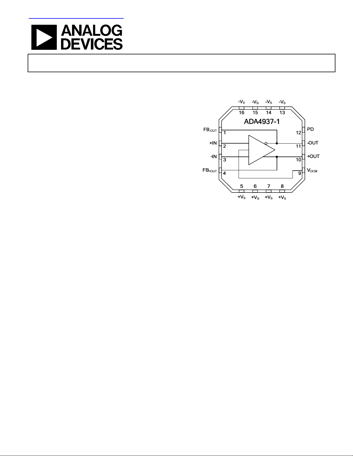
PIN CONFIGURATION AND FUNCTION DESCRIPTIONS
PIN 1
-OUT
+OUT
1FB
2+IN
3-IN
4FB
INDICATOR
TOP VIEW
12 PD
11 -OUT
10 +OUT
9V
OCM
Figure 3. Pin Configuration
Table 5. Pin Function Descriptions
Pin No. Mnemonic Description
1 FB Negative output feedback pin B
-OUT
2 +IN Positive input summing node
3 −IN Negative input summing node
4 FBB
5 to 8 +V
9 V
+OUT
S
OCM
Positive output feedback pin
Positive supply voltage
Output common mode voltage
10 +OUT Positive output
11 −OUT Negative output
12
13 to 16 −V Negative supply voltage
PD
S
Power-down pin
Rev. PrA | Page 8 of 9

Preliminary Technical Data ADA4937-1
OUTLINE DIMENSIONS
0.50
0.40
PAD
0.30
16
1
4
5
N
I
P
D
I
N
I
*
1.65
1.50 SQ
1.35
0.25 MIN
1
R
O
A
T
C
PIN 1
INDICATO
0.90
0.85
0.80
SEATING
PLANE
R
12° MAX
3.00
BSC SQ
TOP
VIEW
0.30
0.23
0.18
*
COMPLIANT
EXCEPT FOR EXPOSED PAD DIMENSION.
2.75
BSC SQ
0.80 MAX
0.65 TYP
0.05 MAX
0.02 NOM
0.20 REF
TO
JEDEC STANDARDS MO-220-VEED-2
0.45
0.50
BSC
1.50 REF
0.60 MAX
12
9
13
EXPOSED
(BOT TOM VIEW)
8
Figure 4. 16-Lead Lead Frame Chip Scale Package [LFCSP_VQ]
3 mm × 3 mm Body
(CP-16-3)
Dimensions shown in millimeters
ORDERING GUIDE
Model Ordering Quantity Temperature Range Package Description Package Option Branding
ADA4937-1YCPZ-R2 5,000 −40°C to +105°C 16-Lead 3 mm × 3 mm LFCSP CP-16 -3 H1S
ADA4937-1YCPZ-RL 1,500 −40°C to +105°C 16-Lead 3 mm × 3 mm LFCSP CP-16 -3 H1S
ADA4937-1YCPZ-R7 250 −40°C to +105°C 16-Lead 3 mm × 3 mm LFCSP CP-16 -3 H1S
©2006 Analog Devices, Inc. All rights reserved. Trademarks and
registered trademarks are the property of their respective owners.
PR06591-0-12/06(PrA)
T TTT
Rev. PrA | Page 9 of 9
 Loading...