

Ultralow Noise
Drivers for Low Voltage ADCs
ADA4930-1/ADA4930-2
FEATURES
Low input voltage noise: 1.2 nV/√Hz
Low common-mode output: 0.9 V on single supply
Extremely low harmonic distortion
−104 dBc HD2 at 10 MHz
−79 dBc HD2 at 70 MHz
−73 dBc HD2 at 100 MHz
−101 dBc HD3 at 10 MHz
−82 dBc HD3 at 70 MHz
−75 dBc HD3 at 100 MHz
High speed
−3 dB bandwidth of 1.35 GHz, G = 1
Slew rate: 3400 V/μs, 25% to 75%
0.1 dB gain flatness to 380 MHz
Fast overdrive recovery of 1.5 ns
0.5 mV typical offset voltage
Externally adjustable gain
Differential-to-differential or single-ended-to-differential
operation
Adjustable output common-mode voltage
Single-supply operation: 3.3 V or 5 V
APPLICATIONS
ADC drivers
Single-ended-to-differential converters
IF and baseband gain blocks
Differential buffers
Line drivers
GENERAL DESCRIPTION
The ADA4930-1/ADA4930-2 are very low noise, low distortion,
high speed differential amplifiers. They are an ideal choice for
driving 1.8 V high performance ADCs with resolutions up to
14 bits from dc to 70 MHz. The adjustable output common
mode allows the ADA4930-1/ADA4930-2 to match the input of
the ADC. The internal common-mode feedback loop provides
exceptional output balance, suppression of even-order harmonic
distortion products, and dc level translation.
With the ADA4930-1/ADA4930-2, differential gain configurations
are easily realized with a simple external feedback network of
four resistors determining the closed-loop gain of the amplifier.
The ADA4930-1/ADA4930-2 are fabricated using Analog Devices,
Inc., proprietary silicon-germanium (SiGe), complementary
bipolar process, enabling them to achieve very low levels of
distortion with an input voltage noise of only 1.2 nV/√Hz.
Rev. A
Information furnished by Analog Devices is believed to be accurate and reliable. However, no
responsibility is assumed by Analog Devices for its use, nor for any infringements of patents or other
rights of third parties that may result from its use. Specifications subject to change without notice. No
license is granted by implication or otherwise under any patent or patent rights of Analog Devices.
Trademarks and registered trademarks are the property of their respective owners.
The low dc offset and excellent dynamic performance of the
ADA4930-1/ADA4930-2 make them well suited for a wide
variety of data acquisition and signal processing applications.
The ADA4930-1 is available in a Pb-free, 3 mm × 3 mm 16-lead
LFCSP, and the ADA4930-2 is available in a Pb-free, 4 mm × 4 mm
24-lead LFCSP. The pinout has been optimized to facilitate printed
circuit board (PCB) layout and minimize distortion. The ADA4930-1
is specified to operate over the −40°C to +105°C temperature range,
and the ADA4930-2 is specified to operate over the −40°C to +105°C
temperature range for 3.3 V or 5 V supply voltages.
One Technology Way, P.O. Box 9106, Norwood, MA 02062-9106, U.S.A.
Tel: 781.329.4700 www.analog.com
Fax: 781.461.3113 ©2010 Analog Devices, Inc. All rights reserved.
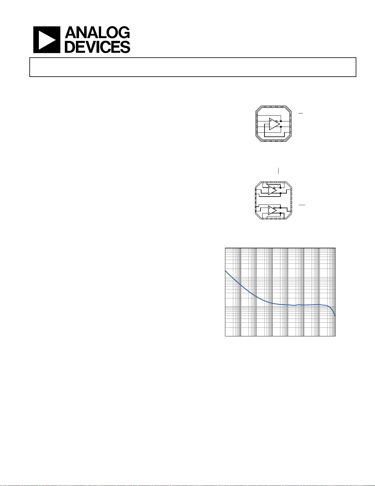
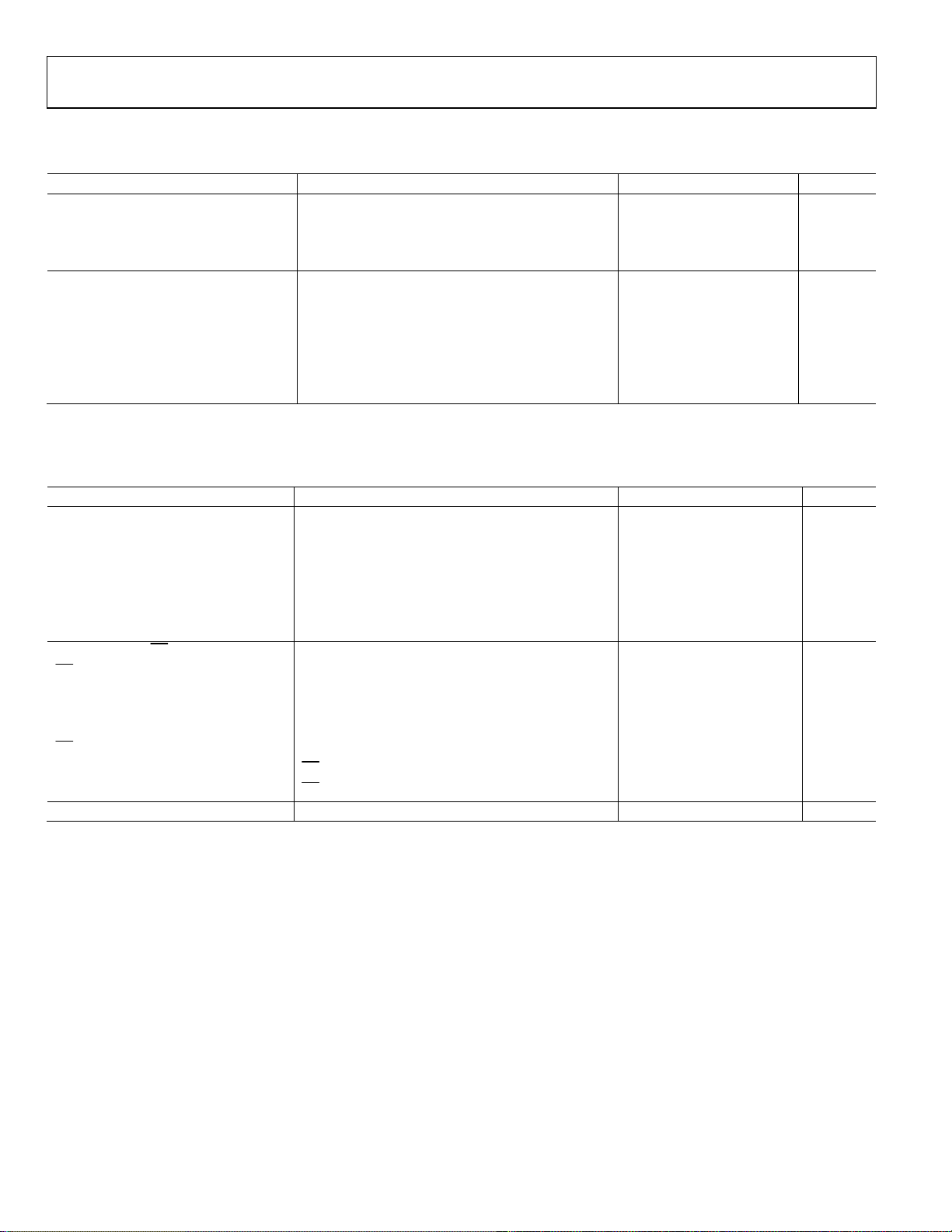
FUNCTIONAL BLOCK DIAGRAMS
1–FB
2+IN
3–IN
4+FB
S
S
S
–V
–V
–V
14
15
16
ADA4930-1
7
5
6
S
S
S
+V
+V
+V
–V
13
8
+V
S
S
12 PD
11 –OUT
10 +OUT
9V
OCM
09209-001
Figure 1.
S1
S1
–OUT1
–V
–V
–FB1
PD1
+IN1
19
20
21
22
23
24
S1
S1
1–IN1
2+FB1
3+V
ADA4930-2
4+V
5–FB2
6+IN2
9
7
8
S2
–IN2
+V
+FB2
18 +O UT1
17 V
OCM1
16 –V
S2
–V
15
S2
14
PD2
13 –OUT2
11
12
10
2
S2
+V
OCM
V
+OUT2
09209-002
Figure 2.
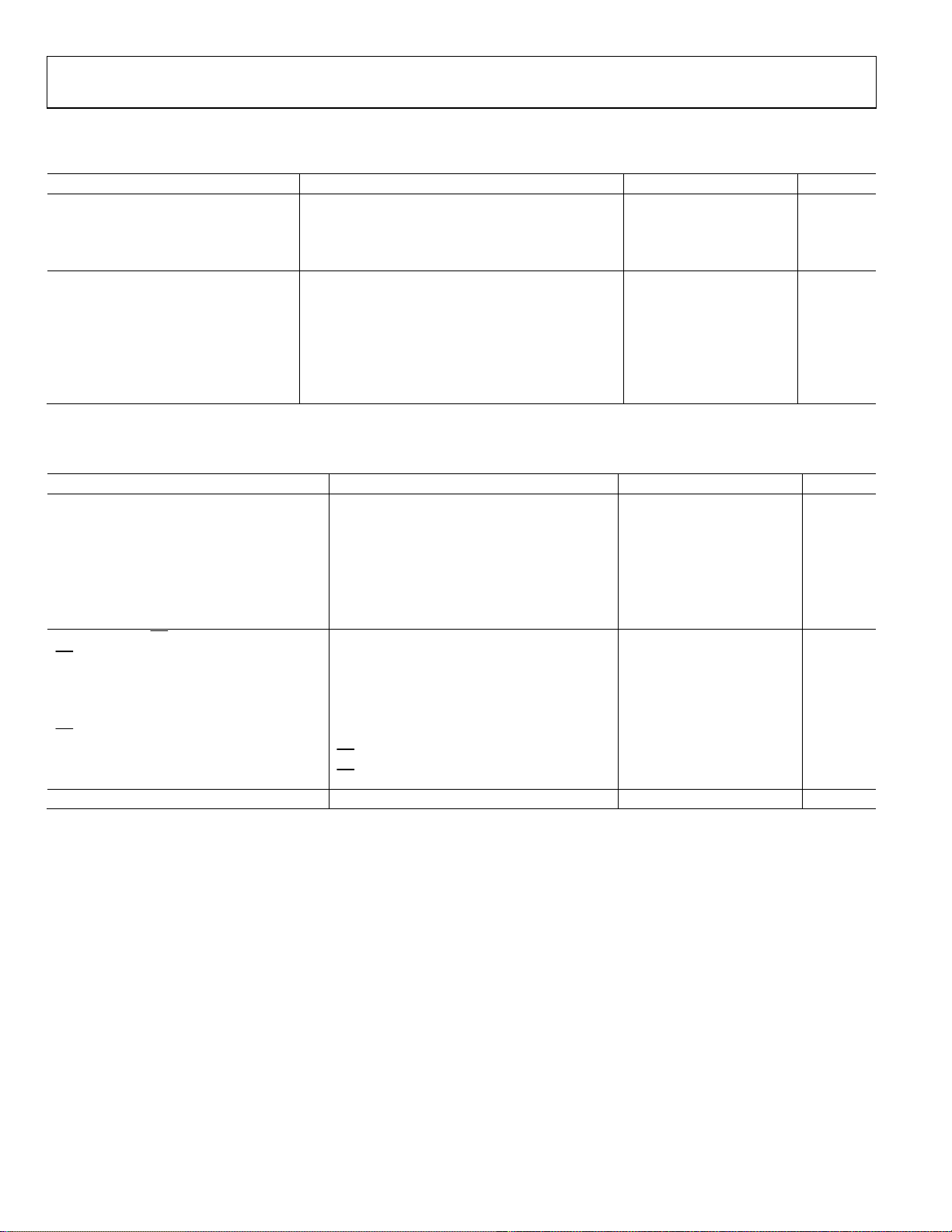
100
10
hz)
(nV/
N
V
1
0
10 100 1k 10k 100k 1M 10M 100M
FREQUENCY (Hz)
Figure 3. Voltage Noise Spectral Density
09209-003

ADA4930-1/ADA4930-2
TABLE OF CONTENTS
Features .............................................................................................. 1
Applications ....................................................................................... 1
General Description ......................................................................... 1
Functional Block Diagrams ............................................................. 1
Revision History ............................................................................... 2
Specifications ..................................................................................... 3
3.3 V Operation ............................................................................ 3
3.3 V V
OCM
to V
Performance ............................................... 4
O, cm
3.3 V General Performance ......................................................... 4
5 V Operation ............................................................................... 5
5 V V
OCM
to V
Performance .................................................. 6
O, cm
5 V General Performance ............................................................ 6
Absolute Maximum Ratings ............................................................ 7
Thermal Resistance ...................................................................... 7
Maximum Power Dissipation ..................................................... 7
ESD Caution .................................................................................. 7
Pin Configurations and Function Descriptions ........................... 8
Typical Performance Characteristics ............................................. 9
Test Circuits ..................................................................................... 15
Operational Description ................................................................ 16
Definition of Terms .................................................................... 16
Theory of Operation ...................................................................... 17
Analyzing an Application Circuit ............................................ 17
Setting the Closed-Loop Gain .................................................. 17
Estimating the Output Noise Voltage ...................................... 17
Impact of Mismatches in the Feedback Networks ................. 18
Input Common-Mode Voltage Range ..................................... 18
Minimum RG Value .................................................................... 19
Setting the Output Common-Mode Voltage .......................... 19
Calculating the Input Impedance for an Application Circuit
....................................................................................................... 19
Layout, Grounding, and Bypassing .............................................. 23
High Performance ADC Driving ................................................. 24
Outline Dimensions ....................................................................... 25
Ordering Guide .......................................................................... 25
REVISION HISTORY
10/10—Rev. 0 to Rev. A
Changes to General Description .................................................... 1
10/10—Revision 0: Initial Version
Rev. A | Page 2 of 28

ADA4930-1/ADA4930-2
SPECIFICATIONS
3.3 V OPERATION
VS = 3.3 V, V
T
= −40°C to +105°C, unless otherwise noted.
MAX
Table 1.
Parameter Test Conditions/Comments Min Typ Max Unit
DYNAMIC PERFORMANCE
−3 dB Small Signal Bandwidth V
−3 dB Large Signal Bandwidth V
Bandwidth for 0.1 dB Flatness V
ADA4930-1 380 MHz
ADA4930-2 89 MHz
Slew Rate V
Settling Time to 0.1% V
Overdrive Recovery Time G = 3, V
NOISE/HARMONIC PERFORMANCE
HD2/HD3 V
V
V
V
Third-Order IMD V
V
Input Voltage Noise f = 100 kHz 1.15 nV/√Hz
Input Current Noise f = 100 kHz 3 pA/√Hz
Crosstalk f = 100 MHz, ADA4930-2, RL = 200 Ω −90 dB
DC PERFORMANCE
Input Offset Voltage VIP = VIN = V
Input Offset Voltage Drift T
Input Bias Current −36 −24 −16 μA
Input Bias Current Drift T
Input Offset Current −1.8 +0.1 +1.8 μA
Open-Loop Gain RF = RG = 10 kΩ, ΔVO = 0.5 V, RL = open circuit 64 dB
INPUT CHARACTERISTICS
Input Common-Mode Voltage Range 0.3 1.2 V
Input Resistance Differential 150 kΩ
Common mode 3 MΩ
Input Capacitance Common mode 1 pF
CMRR ΔV
OUTPUT CHARACTERISTICS
Output Voltage Each single-ended output; RF = RG = 10 kΩ 0.11 1.74 V
Linear Output Current Each single-ended output; f = 1 MHz, TDH ≤ 60 dBc 30 mA
Output Balance Error f = 1 MHz 55 dB
= 0.9 V, V
ICM
= 0.9 V, RF = 301 Ω, RG = 301 Ω, R
OCM
= 0.1 V p-p 1430 MHz
O, dm
= 2 V p-p 887 MHz
O, dm
= 0.1 V p-p
O, dm
= 2 V step, 25% to 75% 2877 V/μs
O, dm
= 2 V step, RL = 200 Ω 6.3 ns
O, dm
= 0.7 V p-p pulse 1.5 ns
IN, dm
= 2 V p-p, fC = 10 MHz −98/−97 dB
O, dm
= 2 V p-p, fC = 30 MHz −91/−88 dB
O, dm
= 2 V p-p, fC = 70 MHz −79/−79 dB
O, dm
= 2 V p-p, fC = 100 MHz −73/−73 dB
O, dm
= 1 V p-p/tone, fC = 70.05 MHz ± 0.05 MHz 91 dBc
O, dm
= 1 V p-p/tone, fC = 140.05 MHz ± 0.05 MHz 86 dBc
O, dm
OCM
to T
MIN
MIN
2.75 μV/°C
MAX
to T
−0.05
MAX
= 0.5 V dc; RF = RG = 10 kΩ, RL = open circuit −82 −77 dB
ICM
= 1 kΩ, single-ended input, differential output, TA = 25°C, T
L, dm
= 0 V, RL = open circuit
to
MIN
−3.1 −0.5 +3.1 mV
μA/°C
Rev. A | Page 3 of 28
ADA4930-1/ADA4930-2
3.3 V V
Table 2.
Parameter Test Conditions/Comments Min Typ Max Unit
V
DYNAMIC PERFORMANCE
OCM
−3 dB Bandwidth V
Slew Rate V
V
INPUT CHARACTERISTICS
OCM
Input Voltage Range 0.8 1.1 V
Input Resistance 7.0 8.3 10.3 kΩ
Input Offset Voltage V
Input Voltage Noise f = 100 kHz 23.5 nV/√Hz
Gain 0.99 1 1.02 V/V
CMRR ΔV
3.3 V GENERAL PERFORMANCE
Table 3.
Parameter Test Conditions/Comments Min Typ Max Unit
POWER SUPPLY
Operating Range 3.3 V
Quiescent Current per Amplifier Enabled 32 35 40 mA
Enabled, T
Disabled 0.44 1.8 2.35 mA
+PSRR ΔV
−PSRR ΔV
POWER-DOWN (PD)
PD Input Voltage
Enabled >1.3 V
Turn-Off Time 1 μs
Turn-On Time 12 ns
PD Pin Bias Current
Enabled
Disabled
OPERATING TEMPERATURE RANGE −40 +105 °C
OCM
TO V
PERFORMANCE
O, CM
= 0.1 V p-p 745 MHz
O, cm
= 2 V p-p, 25% to 75% 828 V/μs
O, cm
= V
− V
OS, cm
O, cm
= 0.5 V dc; RF = RG = 10 kΩ, RL = open circuit −83 −77 dB
OCM
MIN
= 0.5 V; RF = RG = 10 kΩ, RL = open circuit −74 −70 dB
ICM
= 0.5 V; RF = RG = 10 kΩ, RL = open circuit −87 −76 dB
ICM
; VIP = VIN = V
OCM
to T
variation 81
MAX
= 0 V −25 +15.4 +31 mV
OCM
μA/°C
Disabled <0.8 V
PD
PD
= 3.3 V
= 0 V
0.09 μA
97 μA
Rev. A | Page 4 of 28

ADA4930-1/ADA4930-2
5 V OPERATION
VS = 5 V, V
T
to T
MIN
Table 4.
Parameter Test Conditions/Comments Min Typ Max Unit
DYNAMIC PERFORMANCE
−3 dB Small Signal Bandwidth V
−3 dB Large Signal Bandwidth V
Bandwidth for 0.1 dB Flatness V
ADA4930-1 369 MHz
ADA4930-2 90 MHz
Slew Rate V
Settling Time to 0.1% V
Overdrive Recovery Time G = 3, V
NOISE/HARMONIC PERFORMANCE
HD2/HD3 V
V
V
V
Third-Order IMD V
V
Input Voltage Noise f = 100 kHz 1.2 nV/√Hz
Input Current Noise f = 100 kHz 2.8 pA/√Hz
Crosstalk f = 100 MHz, ADA4930-2, RL = 200 Ω −90 dB
DC PERFORMANCE
Input Offset Voltage VIP = VIN = V
Input Offset Voltage Drift T
Input Bias Current −34 −23 −15 μA
Input Bias Current Drift T
Input Offset Current −0.82 +0.1 +0.82 μA
Open-Loop Gain RF = RG = 10 kΩ, ΔVO = 1 V, RL = open circuit 64 dB
INPUT CHARACTERISTICS
Input Common-Mode Voltage Range 0.3 2.8 V
Input Resistance Differential 150 kΩ
Common mode 3 MΩ
Input Capacitance Common mode 1 pF
CMRR ΔV
OUTPUT CHARACTERISTICS
Output Voltage Each single-ended output; RF = RG = 10 kΩ 0.18 3.38 V
Linear Output Current Each single-ended output; f = 1 MHz, TDH ≤ 60 dBc 30 mA
Output Balance Error f = 1 MHz 55 dB
= 0.9 V, V
ICM
= −40°C to +105°C, unless otherwise noted.
MAX
= 0.9 V, RF = 301 Ω, RG = 301 Ω, R
OCM
= 0.1 V p-p 1350 MHz
O, dm
= 2 V p-p 937 MHz
O, dm
= 0.1 V p-p
O, dm
= 2 V step, 25% to 75% 3400 V/μs
O, dm
= 2 V step, RL = 200 Ω 6 ns
O, dm
IN, dm
= 2 V p-p, fC = 10 MHz −104/−101 dB
O, dm
= 2 V p-p, fC = 30 MHz −91/−93 dB
O, dm
= 2 V p-p, fC = 70 MHz −79/−82 dB
O, dm
= 2 V p-p, fC = 100 MHz −73/−75 dB
O, dm
= 1 V p-p/tone, fC = 70.05 MHz ± 0.05 MHz 94 dBc
O, dm
= 1 V p-p/tone, fC = 140.05 MHz ± 0.05 MHz 90 dBc
O, dm
to T
MIN
MAX
to T
MIN
MAX
= 1 V dc; RF = RG = 10 kΩ, RL = open circuit −82 −77 dB
ICM
= 1 kΩ, single-ended input, differential output, TA= 25°C,
L, dm
= 0.7 V p-p pulse 1.5 ns
= 0 V, RL = open circuit
OCM
−3.1 −0.15 +3.1 mV
1.8 μV/°C
−0.05
μA/°C
Rev. A | Page 5 of 28
ADA4930-1/ADA4930-2
5 V V
Table 5.
Parameter Test Conditions/Comments Min Typ Max Unit
V
OCM
V
OCM
5 V GENERAL PERFORMANCE
Table 6.
Parameter Test Conditions/Comments Min Typ Max Unit
POWER SUPPLY
POWER-DOWN (PD)
PD Input Voltage
Turn-Off Time 1 μs
Turn-On Time 12 ns
PD Pin Bias Current
OPERATING TEMPERATURE RANGE −40 +105 °C
OCM
TO V
PERFORMANCE
O, CM
DYNAMIC PERFORMANCE
−3 dB Bandwidth V
Slew Rate V
= 0.1 V p-p 740 MHz
O, cm
= 2 V p-p, 25% to 75% 1224 V/μs
O, cm
INPUT CHARACTERISTICS
Input Voltage Range 0.5 2.3 V
Input Resistance 7.0 8.3 10.2 kΩ
Input Offset Voltage V
OS, cm
= V
O, cm
− V
; VIP = VIN = V
OCM
= 0 V −25 +0.35 +15 mV
OCM
Input Voltage Noise f = 100 kHz 23.5 nV/√Hz
Gain 0.99 1 1.02 V/V
CMRR ΔV
= 1.5 V; RF = RG = 10 kΩ, RL = open circuit −80 −77 dB
OCM
Operating Range 5 V
Quiescent Current per Amplifier Enabled 31.1 34 38.4 mA
Enabled, T
MIN
to T
variation 74.5
MAX
μA/°C
Disabled 0.45 1.8 2.6 mA
+PSRR ΔV
−PSRR ΔV
= 1 V; RF = RG = 10 kΩ, RL = open circuit −74 −71 dB
ICM
= 1 V; RF = RG = 10 kΩ, RL = open circuit −91 −75 dB
ICM
Disabled <2.5 V
Enabled >3 V
Enabled
Disabled
PD
PD
= 5 V
= 0 V
0.09 μA
97 μA
Rev. A | Page 6 of 28
ADA4930-1/ADA4930-2
ABSOLUTE MAXIMUM RATINGS
Table 7.
Parameter Rating
Supply Voltage 5.5 V
Power Dissipation See Figure 4
Storage Temperature Range −65°C to +125°C
Operating Temperature Range −40°C to +105°C
Lead Temperature (Soldering, 10 sec) 300°C
Junction Temperature 150°C
Stresses above those listed under Absolute Maximum Ratings
may cause permanent damage to the device. This is a stress rating
only; functional operation of the device at these or any other
conditions above those indicated in the operational section of
this specification is not implied. Exposure to absolute maximum
rating conditions for extended periods may affect device reliability.
THERMAL RESISTANCE
θJA is specified for the device (including exposed pad) soldered
to a high thermal conductivity 2s2p circuit board, as described
in EIA/JESD51-7.
Table 8. Thermal Resistance
Package Type θJA Unit
16-Lead LFCSP (Exposed Pad) 98 °C/W
24-Lead LFCSP (Exposed Pad) 67 °C/W
MAXIMUM POWER DISSIPATION
The maximum safe power dissipation in the ADA4930-1/ADA4930-2
packages is limited by the associated rise in junction temperature (T
on the die. At approximately 150°C, which is the glass transition
temperature, the plastic changes its properties. Even temporarily
exceeding this temperature limit can change the stresses that the
package exerts on the die, permanently shifting the parametric
performance of the ADA4930-1/ADA4930-2. Exceeding a
junction temperature of 150°C for an extended period can result
in changes in the silicon devices, potentially causing failure.
)
J
The power dissipated in the package (P
quiescent power dissipation and the power dissipated in the
package due to the load drive. The quiescent power is the voltage
between the supply pins (V
) times the quiescent current (IS).
S
The power dissipated due to the load drive depends upon the
particular application. The power due to load drive is calculated
by multiplying the load current by the associated voltage drop
across the device. RMS voltages and currents must be used in
these calculations.
Airflow increases heat dissipation, effectively reducing θ
addition, more metal directly in contact with the package leads/
exposed pad from metal traces, through holes, ground, and
power planes reduces θ
.
JA
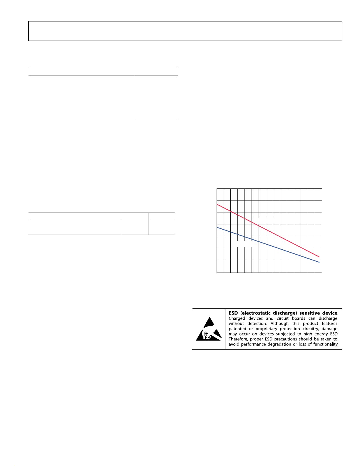
Figure 4 shows the maximum safe power dissipation vs. the
ambient temperature for the ADA4930-1 single 16-lead LFCSP
(98°C/W) and the ADA4930-2 dual 24-lead LFCSP (67°C/W)
on a JEDEC standard 4-layer board.
3.5
3.0
2.5
2.0
1.5
1.0
MAXIMUM POWER DISSIPATION (W)
0.5
0
–40 11090 100
Figure 4. Maximum Power Dissipation vs. Ambient Temperature,
ADA4930-1
–30–20–100 1020304050607080
ADA4930-2
TEMPERATURE (° C)
4-Layer Board
ESD CAUTION
) is the sum of the
D
JA
. In
09209-004
Rev. A | Page 7 of 28
ADA4930-1/ADA4930-2
PIN CONFIGURATIONS AND FUNCTION DESCRIPTIONS
S
S
S
S
–V
–V
–V
–V
14
13
15
16
PIN 1
INDICATO R
1–FB
2+IN
ADA4930-1
TOP VIEW
3–IN
(Not to Scale)
4+FB
8
7
5
6
S
S
S
S
+V
+V
+V
+V
NOTES
1. EXPOSED PADDLE. THE EXPOSED PAD IS NO T
ELECTRICALLY CONNECTED T O THE DEVI CE. IT I S
TYPICALLY SOLDERED T O GROUND OR A POWER
PLANE ON THE PCB THAT IS T HERMALLY CONDUCTIVE.
Figure 5. ADA4930-1 Pin Configuration
12 PD
11 –OUT
10 +OUT
9V
OCM
1
–IN1
2
+FB1
3
+V
S1
4
+V
S1
5
–FB2
6
+IN2
NOTES
1. EXPO SED PADDLE. T HE EXPOSED PAD IS NOT
ELECTRICALLY CONNECTED T O THE DEVI CE. IT I S
09209-005
TYPICALLY SOLDERED TO GROUND OR A POWER
PLANE ON THE PCB THAT IS THERMALLY CONDUCTIVE.
Figure 6. ADA4930-2 Pin Configuration
–VS1–VS1–FB1
+IN1
20
21
22
23
24
PIN 1
INDICATOR
ADA4930-2
TOP VIEW
(Not to Scale)
9
7
8
11
10
S2
S2
–IN2
+V
+V
+FB2
V
PD1
–OUT1
19
18
+OUT1
17
V
OCM1
16
–V
S2
–V
15
S2
14
PD2
13
–OUT2
12
OCM2
+OUT2
9209-006
Table 9. ADA4930-1 Pin Function Descriptions
Pin No. Mnemonic Description
1 −FB
Negative Output for Feedback
Component Connection.
2 +IN Positive Input Summing Node.
3 −IN Negative Input Summing Node.
4 +FB
Positive Output for Feedback
Component Connection.
5 to 8 +VS Positive Supply Voltage.
9 V
Output Common-Mode Voltage.
OCM
10 +OUT Positive Output for Load Connection.
11 −OUT Negative Output for Load Connection.
12
PD
Power-Down Pin.
13 to 16 −VS Negative Supply Voltage.
EPAD
Exposed Paddle. The exposed pad is not
electrically connected to the device. It is
typically soldered to ground or a power
plane on the PCB that is thermally
conductive.
Table 10. ADA4930-2 Pin Function Descriptions
Pin No. Mnemonic Description
1 −IN1 Negative Input Summing Node 1.
2 +FB1 Positive Output Feedback Pin 1.
3, 4 +V
5 −FB2
6 +IN2
7 −IN2
8 +FB2
9, 10 +V
11 V
12 +OUT2
13 −OUT2
14
Positive Supply Voltage 1.
S1
Negative Output Feedback Pin 2.
Positive Input Summing Node 2.
Negative Input Summing Node 2.
Positive Output Feedback Pin 2.
Positive Supply Voltage 2.
S2
Output Common-Mode Voltage 2.
OCM2
Positive Output 2.
Negative Output 2.
PD2
Power-Down Pin 2.
15, 16 −VS2 Negative Supply Voltage 2.
17 V
18 +OUT1
19 −OUT1
20
21, 22 −V
23 −FB1
24 +IN1
EPAD
Output Common-Mode Voltage 1.
OCM1
Positive Output 1.
Negative Output 1.
PD1
Negative Supply Voltage 1.
S1
Power-Down Pin 1.
Negative Output Feedback Pin 1.
Positive Input Summing Node 1.
Exposed Paddle. The exposed pad is
not electrically connected to the
device. It is typically soldered to
ground or a power plane on the PCB
that is thermally conductive.
Rev. A | Page 8 of 28
ADA4930-1/ADA4930-2
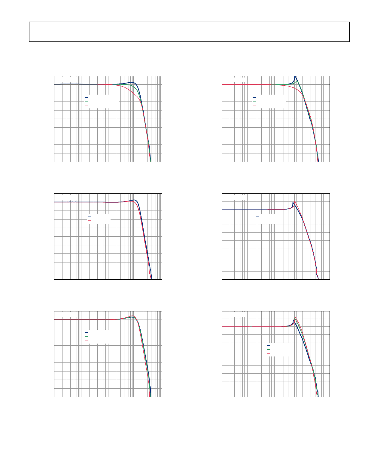
TYPICAL PERFORMANCE CHARACTERISTICS
TA = 25°C, VS = 5 V, V
3
VIN = 100mV
0
–3
–6
–9
–12
–15
–18
–21
NORMALIZE D CLOSED LO OP GAIN (dB)
–24
–27
1M 10M 100M 1G 10G
Figure 7. Small Signal Frequency Response
at Gain = 1, Gain = 2, and Gain = 5
3
VIN = 100mV
0
–3
–6
–9
–12
–15
–18
CLOSED LOOP GAIN (dB)
–21
–24
–27
1M 10M 100M 1G 10G
Figure 8. Small Signal Frequency Response
3
VIN = 100mV
0
–3
–6
–9
–12
–15
–18
CLOSED LOOP GAIN (dB)
–21
–24
–27
1M 10M 100M 1G 10G
Figure 9. Small Signal Frequency Response
at T
= −40°C, TA = 25°C, and TA = 105°C
A
= 0.9 V, V
ICM
G = 1, RG = 300
G = 2, RG = 150
G = 5, RG = 60
FREQUENCY (Hz)
VS = 3.3V
VS = 5.0V
FREQUENCY (Hz)
= 3.3 V and VS = 5 V
at V
S
TA = –40°C
TA = +25°C
T
= +105°C
A
FREQUENCY (Hz)
= 0.9 V, R
OCM
= 1 kΩ, unless otherwise noted.
L, dm
9209-007
9209-008
9209-009
3
VIN = 2V p-p
0
–3
–6
–9
–12
–15
–18
–21
NORMALIZED CLOSED LOOP GAIN (dB)
–24
–27
1M 10M 100M 1G 10G
G = 1, RG = 300
G = 2, R
= 150
G
G = 5, RG = 60
FREQUENCY (Hz)
Figure 10. Large Signal Frequency Response
at Gain = 1, Gain = 2, and Gain = 5
6
VIN = 2V p-p
3
0
–3
–6
–9
–12
–15
–18
CLOSED LOOP GAIN (dB)
–21
–24
–27
1M 10M 100M 1G 10G
VS = 3.3V
VS = 5.0V
FREQUENCY (Hz)
Figure 11. Large Signal Frequency Response
= 3.3 V and VS = 5 V
at V
S
6
VIN = 2V p-p
3
0
–3
–6
–9
–12
–15
–18
CLOSED LOOP GAIN (dB)
–21
–24
–27
1M 10M 100M 1G 10G
TA = –40°C
TA = +25°C
T
= +105°C
A
FREQUENCY (Hz)
Figure 12. Large Signal Frequency Response
at T
= −40°C, TA = 25°C, and TA = 105°C
A
9209-010
9209-011
9209-012
Rev. A | Page 9 of 28
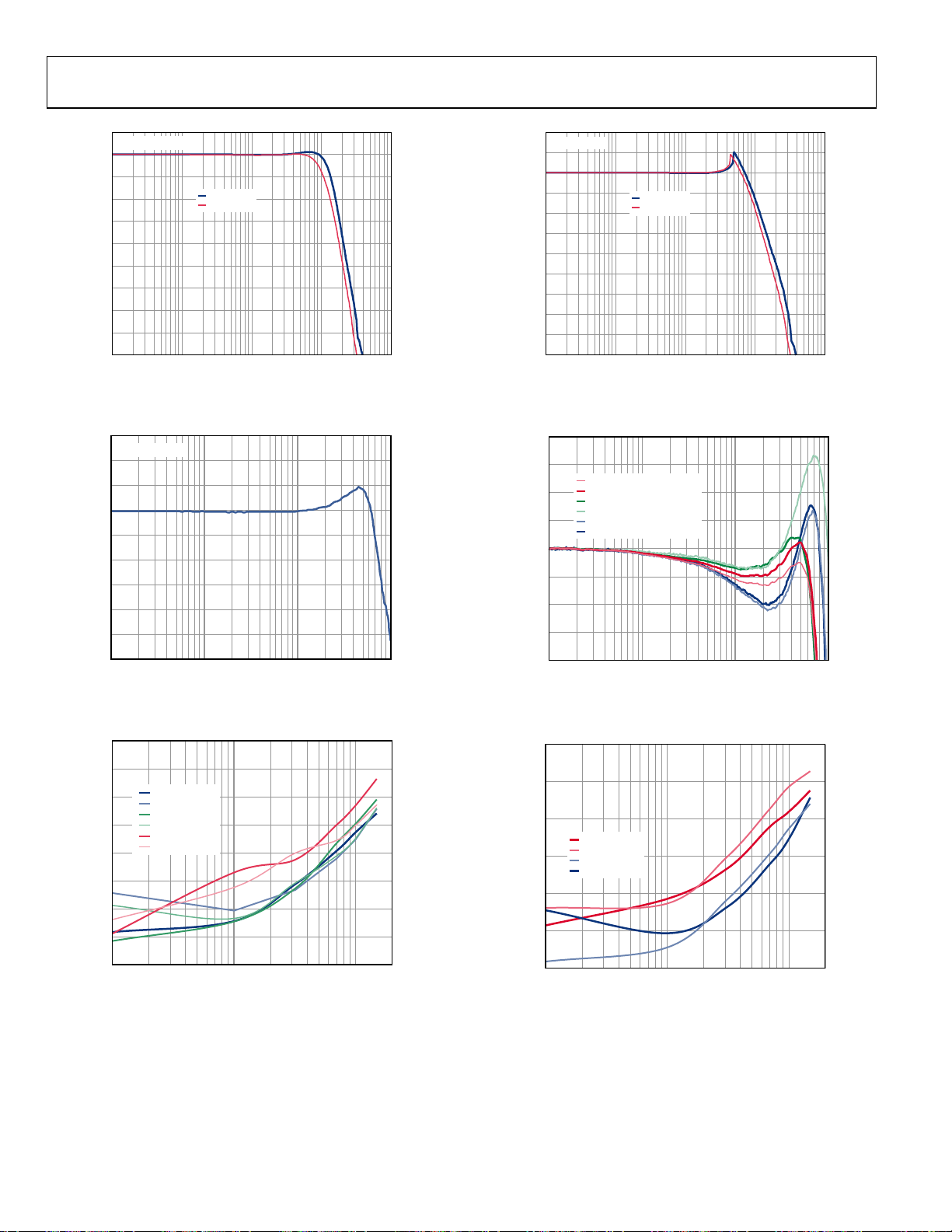
ADA4930-1/ADA4930-2
–
–
3
VIN = 100mV p-p
0
–3
–6
–9
–12
–15
–18
–21
NORMALIZE D CLOSED LO OP GAIN (dB)
–24
–27
1M 10M 100M 1G 10G
RL = 1k
RL = 200
FREQUENCY (Hz)
Figure 13. Small Signal Frequency Response for RL = 200 Ω and RL = 1 kΩ
3
VIN = 100mV
2
1
0
–1
GAIN (dB)
–2
–3
–4
–5
–6
1M 10M 100M
Figure 14. V
FREQUENCY (Hz)
Small Signal Frequency Response
OCM
1G
09209-014
40
–50
HD2, GAIN = 1
HD3, GAIN = 1
HD2, GAIN = 2
HD3, GAIN = 2
HD2, GAIN = 5
HD3, GAIN = 5
DISTORTION (dBc)
–60
–70
–80
–90
–100
–110
9209-013
6
VIN = 2V p-p
3
0
–3
–6
–9
–12
–15
–18
CLOSED-LOOP GAIN (dB)
–21
–24
–27
1M 10M 100M 1G 10G
RL = 1k
RL = 200
FREQUENCY (Hz)
Figure 16. Large Signal Frequency Response
= 200 Ω and RL = 1 kΩ
for R
L
0.4
0.3
ADA4930-2, 200, OUT 1
0.2
0.1
0
GAIN (dB)
–0.1
–0.2
–0.3
–0.4
ADA4930-2, 200, OUT 2
ADA4930-1, 200
ADA4930-1, 1k
ADA4930-2, 1k, OUT 1
ADA4930-2, 1k, OUT 2
1M 10M 100M 1G
FREQUENCY (Hz)
Figure 17. Small Signal 0.1 dB Flatness vs. Frequency for
R
= 200 Ω and RL = 1 kΩ
L
50
–60
–70
HD2, RL = 200
HD3, RL = 200
HD2, R
= 1k
L
HD3, RL = 1k
DISTORTION (dBc)
–80
–90
–100
9209-016
09209-017
–120
1M 10M 100M 200M
FREQUENCY ( Hz)
Figure 15. Harmonic Distortion vs. Frequency
for Gain = 1, Gain = 2, and Gain = 5
09209-015
–110
1M 10M 100M 200M
FREQUENCY (Hz)
Figure 18. Harmonic Distortion vs. Frequency
= 200 Ω and RL = 1 kΩ
for R
L
09209-018
Rev. A | Page 10 of 28

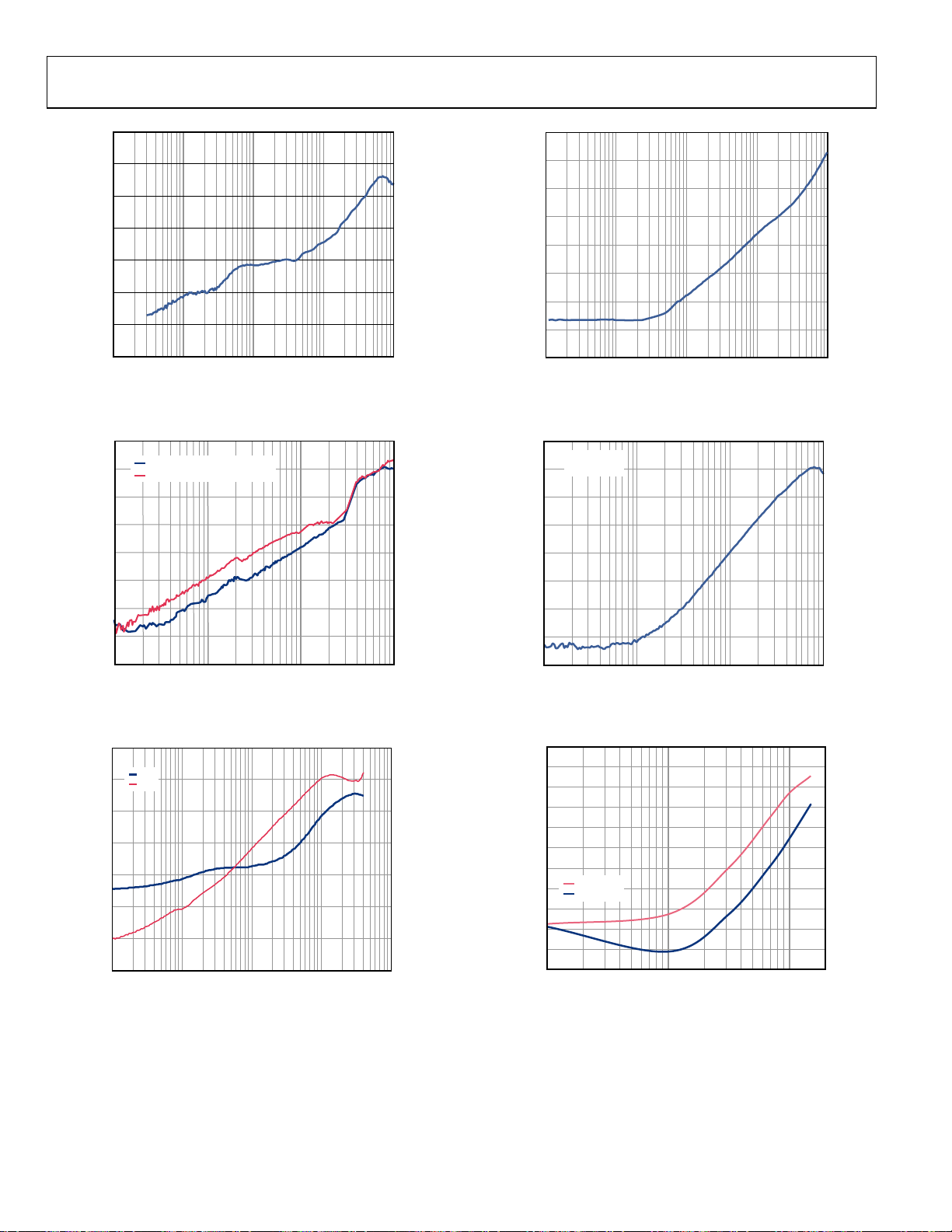
ADA4930-1/ADA4930-2
–
–
–
–
60
–65
–70
–75
–80
–85
–90
DISTORTION (dBc)
–95
–100
–105
–110
HD2, VS = 3.3V
HD3, VS = 3.3V
HD2, VS = 5.0V
HD3, VS = 5.0V
1M 10M 100M 200M
FREQUENCY ( Hz)
Figure 19. ADA4930-1 Harmonic Distortion vs. Frequency
= 3.3 V and VS = 5 V
at V
S
DISTORTION (dBc)
40
–50
–60
–70
–80
–90
–100
–110
10MHz, HD2
10MHz, HD3
70MHz, HD2
70MHz, HD3
09209-019
20
–40
–60
HD2, 3.3V
HD3, 3.3V
HD2, 5.0V
HD3, 5.0V
1.0 1.5 2.0 2.5 3.0 3. 5
V
(V p-p)
OUT
DISTORTON (d Bc)
–80
–100
–120
–140
Figure 22. Harmonic Distortion vs. Output @ 10 MHz
40
–50
10MHz, HD2
10MHz, HD3
70MHz, HD2
70MHz, HD3
DISTORTION (dBc)
–100
–60
–70
–80
–90
09209-022
–120
0.40.50.60.70.80.91.01.11.2
Figure 20. Harmonic Distortion vs. V
V
ABOVE – VS(V)
OCM
at VS = 3.3 V
OCM
at 10 MHz and 70 MHz
0
–20
–40
–60
–80
DISTOTION (dBc)
–100
–120
–140
1M 10M 100M 200M
FREQUENCY (Hz)
Figure 21. Distortion vs. V
HD2, V
HD3, V
HD2, V
HD3, V
at VS = 3.3 V
OUT
OUT
OUT
OUT
OUT
= 1V p-p
= 1V p-p
= 2V p-p
= 2V p-p
–110
0.5 1.0 1. 5 2.0 2. 5 3.0
09209-020
Figure 23. Harmonic Distortion vs. V
V
ABOVE – VS(V)
OCM
09209-023
OCM
at 10 MHz and 70 MHz
20
0
–20
–40
–60
–80
–100
NORMALIZED SPECTRUM (d Bc)
–120
–140
69.8 69.9 70.0 70.1 70.2 70.3
09209-021
FREQUENCY (MHz)
9209-024
Figure 24. 70 MHz Intermodulation Distortion
Rev. A | Page 11 of 28
ADA4930-1/ADA4930-2
–
–
–
–
–
40
20
–45
–50
–55
–60
CMRR (dB)
–65
–70
–75
100k 1M 10M 100M 1G
FREQUENCY ( Hz)
Figure 25. CMRR vs. Frequency, RL = 200 Ω
60
–70
–80
–90
–100
–110
CROSSTALK (dB)
–120
CHANNEL 1 TO CHANNE L 2
CHANNEL 2 TO CHANNE L 1
–30
–40
–50
–60
PSRR (dB)
–70
–80
–90
–100
100k 1M 10M 100M 1G
09209-025
FREQUENCY (Hz)
09209-028
Figure 28. PSRR vs. Frequency, RL = 200 Ω
20
VIN = 1V p-p
GAIN = 2
–25
–30
–35
–40
–45
CROSSTALK (d B)
–50
–130
–140
1M 10M 100M
FREQUENCY (Hz)
Figure 26. Crosstalk vs. Frequency, RL = 200 Ω
0
–10
–20
–30
–40
S PARAMETERS (d B)
–50
–60
–70
S11
S22
1M 10M 100M 1G 10G
FREQUENCY (Hz)
Figure 27. S11, S22, RL = 200 Ω
–55
1G
9209-026
–60
1M 10M 100M 1G
FREQUENCY (Hz)
9209-029
Figure 29. Output Balance vs. Frequency, RL = 200 Ω
50
–55
–60
–65
–70
–75
–80
–85
DISTORTIO N (dBc)
–90
–95
–100
–105
9209-027
RL = 200
R
= 1k
L
1M 10M 100M 200M
FREQUENCY ( Hz)
09209-030
Figure 30. SFDR
Rev. A | Page 12 of 28
ADA4930-1/ADA4930-2
80
70
60
50
40
30
20
10
GAIN (dB)
0
–10
–20
–30
–40
10k 100k 1M 10M 100M 1G 10G
FREQUENCY (MHz)
GAIN
PHASE
Figure 31. Open Loop Gain and Phase
0.10
0.05
(V)
0
OUT
V
–0.05
–0.10
0246 1
TIME (ns)
Figure 32. Small Signal Pulse Response
2.0
1.5
1.0
0.5
(V)
0
OUT
V
–0.5
–1.0
–1.5
VO = 2V p-p
V
= 1V p-p
O
60
30
0
30
–60
–90
–120
–150
–180
–210
–240
–270
–300
PHASE (°)
09209-031
100
10
hz)
(nV/
N
V
1
0
10 100 1k 10k 100k 1M 10M 100M
FREQUENCY (Hz)
09209-034
Figure 34. Voltage Noise Spectral Density
1.00
0.98
0.96
0.94
0.92
(V)
0.90
OUT
V
0.88
0.86
0.84
0.82
8
0
09209-032
0.80
02468101214161820
Figure 35. Small Signal V
TIME (ns)
OCM
Pulse Response
09209-035
3.0
2.5
2.0
(V)
1.5
OUT
V
1.0
0.5
–2.0
0
246 1
TIME (ns)
Figure 33. Large Signal Pulse Response
8
0
09209-033
0
02468101214161820
Figure 36. Large Signal V
TIME (ns)
OCM
Pulse Response
09209-036
Rev. A | Page 13 of 28

ADA4930-1/ADA4930-2
T
2.25
2.00
1.75
1.50
1.25
1.00
AGE (V)
0.75
VOL
0.50
0.25
0
–0.25
0 100 200 300 40 0 500 600 700 800 900 1000
Figure 37.
TIME (ns)
PD
Response vs. Time
PD
+OUT
–OUT
9209-037
2.5
2.0
1.5
1.0
0.5
0
–0.5
VOLTAGE (V)
–1.0
–1.5
–2.0
–2.5
0 5 10 15 20 25 30 35 40 45 50
Figure 38. V
VIN × 3
V
O, dm
TIME (ns)
Overdrive Recovery
o, dm
09209-038
Rev. A | Page 14 of 28

ADA4930-1/ADA4930-2
TEST CIRCUITS
301
+V
S
30150
V
IN
0.9V
57.6
0.9V
0.9V
V
OCM
301
26.7
ADA4930
301
1k
09209-046
Figure 39. Equivalent Basic Test Circuit
301
+V
S
30150
V
IN
0.9V
57.6
0.9V
0.9V
V
OCM
301
26.7
ADA4930
301
50
50
09209-047
Figure 40. Test Circuit for Output Balance
301
+V
S
0.1µF
0.1µF
412
261
412
0.9V
FILTER
09209-048
0.9V
0.9V
30150
V
301
26.7
OCM
ADA4930
301
FILTER
V
IN
0.9V
57.6
Figure 41. Test Circuit for Distortion Measurements
Rev. A | Page 15 of 28

ADA4930-1/ADA4930-2
–
V
OPERATIONAL DESCRIPTION
DEFINITION OF TERMS
FB
R
F
R
G
+D
OCM
–D
+FB
IN
IN
+IN
ADA4930
–IN
R
G
R
F
Figure 42. Circuit Definitions
Differential Voltage
Differential voltage refers to the difference between two
node voltages. For example, the output differential voltage (or,
equivalently, output differential-mode voltage) is defined as
V
where V
OUT, dm
+OUT
= (V
and V
− V
+OUT
−OUT
refer to the voltages at the +OUT and
−OUT
−OUT terminals with respect to a common reference.
–OUT
V
R
OUT, dm
L, dm
+OUT
09209-049
)
Common-Mode Voltage
Common-mode voltage refers to the average of two node voltages.
The output common-mode voltage is defined as
V
OUT, cm
= (V
+OUT
+ V
−OUT
)/2
Balance
Output balance is a measure of how close the differential signals are
to being equal in amplitude and opposite in phase. Output balance
is most easily determined by placing a well-matched resistor divider
between the differential voltage nodes and comparing the magnitude
of the signal at the divider midpoint with the magnitude of the
differential signal (see Figure 39). By this definition, output balance
is the magnitude of the output common-mode voltage divided by
the magnitude of the output differential mode voltage.
V
cmOUT
ErrorBalanceOutput
,
=
V
dmOUT
,
Rev. A | Page 16 of 28

ADA4930-1/ADA4930-2
V
V
THEORY OF OPERATION
The ADA4930-1/ADA4930-2 differ from conventional op amps
in that they have two outputs whose voltages move in opposite
directions and an additional input, V
. Like an op amp, they rely
OCM
on high open-loop gain and negative feedback to force these
outputs to the desired voltages. The ADA4930-1/ADA4930-2
behave much like standard voltage feedback op amps and facilitate
single-ended-to-differential conversions, common-mode level
shifting, and amplifications of differential signals. Like op amps,
the ADA4930-1/ADA4930-2 have high input impedance and low
output impedance.
Two feedback loops control the differential and common-mode
output voltages. The differential feedback, set with external
resistors, controls the differential output voltage. The commonmode feedback controls the common-mode output voltage. This
architecture makes it easy to set the output common-mode level
to any arbitrary value within the specified limits. The output
common-mode voltage is forced to be equal to the voltage applied
to the V
input by the internal common-mode feedback loop.
OCM
The internal common-mode feedback loop produces outputs
that are highly balanced over a wide frequency range without
requiring tightly matched external components. This results
in differential outputs that are very close to the ideal of being
identical in amplitude and are exactly 180°apart in phase.
ANALYZING AN APPLICATION CIRCUIT
The ADA4930-1/ADA4930-2 use high open-loop gain and
negative feedback to force their differential and common-mode
output voltages to minimize the differential and common-mode
error voltages. The differential error voltage is defined as the
voltage between the differential inputs labeled +IN and −IN
(see Figure 42). For most purposes, this voltage can be assumed
to be zero. Similarly, the difference between the actual output
common-mode voltage and the voltage applied to V
can also
OCM
be assumed to be zero. Starting from these two assumptions,
any application circuit can be analyzed.
SETTING THE CLOSED-LOOP GAIN
The differential-mode gain of the circuit in Figure 42 is
determined by
V
V
where the gain and feedback resistors,
are equal.
R
,
dmOUT
F
=
R
,
dmIN
G
R
and RF, on each side
G
ESTIMATING THE OUTPUT NOISE VOLTAGE
The differential output noise of the ADA4930-1/ADA4930-2 can
be estimated using the noise model in Figure 43. The input-referred
noise voltage density, v
currents, i
nIN−
and i
nRG1
V
nRG2
Similar to the case of conventional op amps, the output noise
voltage densities can be estimated by multiplying the inputreferred terms at +IN and −IN by an appropriate output factor.
The output voltage due to v
the noise gain, G
N
The circuit noise gain is
2
=
N
()
ββG+
where the feedback factors are
When the feedback factors are matched, R
β1 = β2 = β, and the noise gain becomes
The noise currents are uncorrelated with the same mean-square
value, and each produces an output voltage that is equal to the
noise current multiplied by the associated feedback resistance.
The noise voltage density at the V
feedback networks have the same feedback factor, as in most
cases, the output noise due to v
output noise from V
Each of the four resistors contributes (4kTR
from the feedback resistors appears directly at the output, and
the noise from the gain resistors appears at the output multiplied
by R
F/RG
.
The total differential output noise density, v
square of the individual output noise terms.
8
=
vv
∑
=
1i
, is modeled as differential. The noise
nIN
, appear between each input and ground.
nIN+
nRF1
R
G1
i
nIN+
i
nIN–
R
G2
R
F1
+
V
nIN
ADA4930
V
OCM
R
F2
V
Figure 43. Noise Model
nIN
nRF2
is obtained by multiplying v
V
nOD
V
nCM
.
21
R
G1
RR
G1
F1/RG1
G +== 1
pin is v
and
β+=
2
= RF2/RG2,
1
N
β
. When the
nCM
1/2
)
. The noise
xx
, is the root-sum-
nOD
nODinOD
OCM
2
)(
β+=
1
is zero.
F1
OCM
is common-mode and the
nCM
09209-050
by
nIN
R
G2
RR
F2
G2
R
F
.
R
G
.
Rev. A | Page 17 of 28

ADA4930-1/ADA4930-2
Table 11. Output Noise Voltage Density Calculations for Matched Feedback Networks
Input Noise
Input Noise Contribution Input Noise Term
Differential Input v
Inverting Input i
Noninverting Input i
V
Input v
OCM
Gain Resistor RG1 v
Gain Resistor RG2 v
Feedback Resistor RF1 v
Feedback Resistor RF2 v
v
nIN
i
nIN+
i
nIN−
v
nCM
(4kTRG1)
nRG1
(4kTRG2)
nRG2
(4kTRF1)
nRF1
(4kTRF2)
nRF2
Voltage Density
G
nIN
× (RF2) 1 v
nIN+
× (RF1) 1 v
nIN−
0 v
nCM
1/2
R
1/2
R
1/2
1 v
1/2
1 v
Table 12. Differential Input, DC-Coupled, VS = 5 V
Nominal Gain (dB) RF1, RF2 (Ω) RG1, RG2 (Ω) R
(Ω) Differential Output Noise Density (nV/√Hz)
IN, dm
0 301 301 602 4.9
6 301 150 300 6.2
10 301 95.3 190.6 7.8
14 301 60.4 120.4 10.1
Table 13. Single-Ended Ground-Referenced Input, DC-Coupled, RS = 50 Ω, VS = 5 V
Nominal Gain (dB) RF1, RF2 (Ω) RG1 (Ω) RT (Ω) R
IN, cm
(Ω) R
0 301 142 64.2 190.67 170 5.9
6 301 63.4 84.5 95.06 95 7.8
10 301 33.2 1 k 53.54 69.3 9.3
14 301 10.2 1.15 k 17.5 57.7 10.4
1
RG2 = RG1 + (RS||RT).
Table 11 summarizes the input noise sources, the multiplication
factors, and the output-referred noise density terms.
Table 12 and Tabl e 13 list several common gain settings, associated
resistor values, input impedance, and output noise density for
both balanced and unbalanced input configurations.
IMPACT OF MISMATCHES IN THE FEEDBACK NETWORKS
As previously mentioned, even if the external feedback networks
(R
) are mismatched, the internal common-mode feedback
F/RG
loop still forces the outputs to remain balanced. The amplitudes
of the signals at each output remain equal and 180° out of phase.
The input-to-output differential mode gain varies proportionately
to the feedback mismatch, but the output balance is unaffected.
The gain from the V
2(β1 − β2)/(β1 + β2)
When β1 = β2, this term goes to zero and there is no differential
output voltage due to the voltage on the V
noise). The extreme case occurs when one loop is open and the
other has 100% feedback; in this case, the gain from V
to V
is either +2 or −2, depending on which loop is closed. The
O, dm
feedback loops are nominally matched to within 1% in most
applications, and the output noise and offsets due to the V
input are negligible. If the loops are intentionally mismatched by a
pin to V
OCM
is equal to
O, dm
input (including
OCM
input
OCM
OCM
Rev. A | Page 18 of 28
Output
Multiplication Factor
v
N
v
F1/RG1
v
F2/RG2
(Ω)1 Differential Output Noise Density (nV/√Hz)
G2
large amount, it is necessary to include the gain term from V
to V
and account for the extra noise. For example, if β1 = 0.5
O, dm
and β2 = 0.25, the gain from V
Differential Output Noise
Voltage Density Terms
= GN(v
OCM
to V
nOD1
nOD2
nOD3
nOD4
nOD5
nOD6
nOD7
nOD8
O, dm
nIN
= (i
)(RF2)
nIN+
= (i
)(RF1)
nIN−
= 0
= (RF1/RG1)(4kTRG1)
= (RF2/RG2)(4kTRG2)
= (4kTRF1)
= (4kTRF2)
is 0.67. If the V
)
1/2
1/2
OCM
OCM
pin
1/2
1/2
is set to 0.9 V, a differential offset voltage is present at the output of
(0.9 V)(0.67) = 0.6 V. The differential output noise contribution is
(5 nV/√Hz)(0.67) = 3.35 nV/√Hz. Both of these results are
undesirable in most applications; therefore, it is best to use
nominally matched feedback factors.
Mismatched feedback networks also result in a degradation of
the ability of the circuit to reject input common-mode signals,
much the same as for a four-resistor difference amplifier made
from a conventional op amp.
As a practical summarization of the previous issues, resistors of
1% tolerance produce a worst-case input CMRR of approximately
40 dB, a worst-case differential-mode output offset of 9 mV due
to a 0.9 V V
input, negligible V
OCM
noise contribution, and
OCM
no significant degradation in output balance error.
INPUT COMMON-MODE VOLTAGE RANGE
The input common-mode range at the summing nodes of the
ADA4930-1/ADA4930-2 is specified as 0.3 V to 1.5 V at V
To avoid nonlinearities, the voltage swing at the +IN and −IN
terminals must be confined to these ranges.
= 3.3 V.
S

ADA4930-1/ADA4930-2
MINIMUM RG VALUE
Due to the wide bandwidth of the ADA4930-1/ADA4930-2, the
value of R
must be greater than or equal to 301 Ω at unity gain
G
to provide sufficient damping in the amplifier front end. In the
terminated case, R
includes the Thevenin resistance of the
G
source and load terminations.
SETTING THE OUTPUT COMMON-MODE VOLTAGE
The V
the total supply voltage above −V
The input impedance of the V
on the internal bias, the output common-mode voltage is within
about 100 mV of the expected value.
In cases where accurate control of the output common-mode
level is required, it is recommended that an external source or
resistor divider be used with source resistance less than 100 Ω.
The output common-mode offset listed in the Specifications
section assumes that the V
voltage source.
It is also possible to connect the V
voltage (V
to ensure that the output has sufficient drive capability. The
input impedance of the V
multiple ADA4930-1/ADA4930-2 devices share one reference
output, it is recommended that a buffer be used.
pin of the ADA4930-1/ADA4930-2 is biased at 3/10 of
OCM
with an internal voltage divider.
S
pin is 8.4 kΩ. When relying
OCM
input is driven by a low impedance
OCM
input to a common-mode
OCM
) output of an ADC. However, care must be taken
CM
pin is approximately 10 kΩ. If
OCM
CALCULATING THE INPUT IMPEDANCE FOR AN APPLICATION CIRCUIT
The effective input impedance depends on whether the signal
source is single-ended or differential. For a balanced differential
input signal, as shown in Figure 44, the input impedance (R
between the inputs (+D
+D
IN
–D
IN
Figure 44. ADA4930-1/ADA4930-2 Configured for Balanced (Differential) Inputs
and −DIN) is R
IN
R
G
+IN
V
OCM
–IN
R
G
R
F
ADA4930
+V
S
R
F
IN, dm
V
= 2 × RG.
OUT, dm
09209-051
)
IN, dm
For an unbalanced single-ended input signal, as shown in
Figure 45, the input impedance is
R
= RG1
IN,SE
β2β1
)1( ++β2β1
where:
β1 =
β2 =
Figure 45. ADA4930-1/ADA4930-2 with Unbalanced (Single-Ended) Input
G1
RRR+
F1
G1
G
RRR+
22F
G2
R
F1
R
IN, SE
R
G1
V
OCM
R
G2
+V
S
ADA4930
–V
S
R
F2
RLV
OUT, dm
9209-052
For a balanced system where RG1 = RG2 = RG and RF1 = RF2 = RF,
the equations simplify to
⎛
R
β2β1
G
==
+
G
Rand
RR
F
IN,SE
⎜
R
⎜
=
⎜
−
1
⎜
⎝
G
⎞
⎟
G
⎟
⎟
R
F
⎟
RR
+
)2(
F
⎠
The input impedance of the circuit is effectively higher than it
would be for a conventional op amp connected as an inverter
because a fraction of the differential output voltage appears at
the inputs as a common-mode signal, partially bootstrapping
the voltage across the input resistor R
. The common-mode
G1
voltage at the amplifier input terminals can be easily determined
by noting that the voltage at the inverting input is equal to the
noninverting output voltage divided down by the voltage divider
formed by R
and RG2. This voltage is present at both input
F2
terminals due to negative voltage feedback and is in phase
with the input signal, thus reducing the effective voltage across
, partially bootstrapping it.
R
G1
Rev. A | Page 19 of 28

ADA4930-1/ADA4930-2
2
p
4.
Terminating a Single-Ended Input
Set R
This section describes the five steps that properly terminate a
single-ended input to the ADA4930-1/ADA4930-2. Assume a
system gain of 1, R
= RF2 = 301 Ω, an input source with an open-
F1
circuit output voltage of 2 V p-p, and a source resistance of 50 Ω.
Figure 46 shows this circuit.
1.
Calculate the input impedance.
β1 = β2 = 301/602 = 0.5 and R
R
IN
401.333
2V p-p
R
S
50
V
S
R
G1
301
V
OCM
R
G2
301
Figure 46. Single-Ended Input Impedance R
2. Add a termination resistor, RT. To match the 50 Ω source
resistance, R
R
= 57.116 .
T
V
S
2V p-p
50
is added. Because RT||401.33 Ω = 50 Ω,
T
R
IN
50
R
S
57.116
R
G1
301
R
T
V
OCM
R
G2
301
Figure 47. Adding Termination Resistor R
= 401.333 Ω
IN
R
F1
301
+V
S
ADA4930
–V
S
R
F2
301
R
F1
301
+V
S
ADA4930
–V
S
R
F2
301
RLV
IN
T
RLV
OUT, dm
OUT, dm
09209-053
1.066V p-p
5. The modified gain resistor, R
9209-054
3. Replace the source-termination resistor combination with
its Thevenin equivalent. The Thevenin equivalent of the
source resistance R
R
= RS||RT = 26.66 . TheThevenin equivalent of the
TH
and the termination resistance RT is
S
source voltage is
= V
V
TH
T
RRR+
S
T
R
S
50
= 1.066 V p-p
R
T
57.116
1.066V p-p
V p-
S
V
S
Figure 48. Thevenin Equivalent Circuit
2V p-p
R
TH
26.661
V
TH
9209-055
Figure 50. Terminated Single-Ended-to-Differential System with G = 1
Rev. A | Page 20 of 28
= RF2 = RF to maintain a balanced system.
F1
Compensate the imbalance caused by R
. There are two
TH
methods available to compensate, which follow:
Add R
•
and increase R
to RG2 to maintain balanced gain resistances
TH
V
S
and RF2 to RF =
F1
Gain(R
V
TH
+ RTH) to
G
maintain the system gain.
×
VR
F
•
Decrease R
gain and decrease R
to RG2 =
G2
to (RG2 − RTH) to maintain
G1
TH
to maintain system
GainV
×
S
balanced gain resistances.
The first compensation method is used in the Diff Amp
Calculator™ tool. Using the second compensation method,
R
= 160.498 Ω and RG1 = 160.498 − 26.66 = 133.837 .
G2
The modified circuit is shown in Figure 49.
R
F1
301
+V
S
R
26.661
V
TH
TH
R
G1
133.837
V
OCM
R
G2
160.498
ADA4930
–V
S
R
F2
301
V
R
OUT, dm
L
09209-056
Figure 49. Thevenin Equivalent with Matched Gain Resistors
Figure 49 presents an easily manageable circuit with matched
feedback loops that can be easily evaluated.
, changes the input impedance.
G1
Repeat Step 1 through Step 4 several times using the modified
value of R
does not change from the previous iteration. After three
R
T
additional iterations, the change in R
from the previous iteration until the value of
G1
is less than 0.1%.
G1
The final circuit is shown in Figure 50 with the closest
0.5% resistor values.
R
F1
301
+V
P
ADA4930
N
R
301
S
V
OUT, dm
R
L
1.990V p-p
–V
S
F2
09209-057
0.998V p-p
R
S
50
V
S
64.2
R
V
G
142
R
T
V
OCM
R
V
G2
169

ADA4930-1/ADA4930-2
3.
Terminating a Single-Ended Input in a Single-Supply Applications
When the application circuit of Figure 50 is powered by a single
supply, the common-mode voltage at the amplifier inputs, V
and V
, may have to be raised to comply with the specified input
N
P
common-mode range. Two methods are available: a dc bias on
the source, as shown in Figure 51, or by connecting resistors R
CM
between each input and the supply, as shown on Figure 54.
Input Common-Mode Adjustment with DC Biased Source
To drive a 1.8 V ADC with VCM = 1 V, a 3.3 V single supply
minimizes the power dissipation of the ADA4930-1/ADA4930-2.
The application circuit of Figure 50 on a 3.3 V single supply with a
dc bias added to the source is shown in Figure 51.
R
F1
301
3.3V
2V p-p
R
S
50
V
S
50
V
DC
64.2
64.2
R
V
G1
P
142
R
T
V
OCM
R
G2
142
V
N
ADA4930
R
F2
301
RLV
OUT, dm
1.990V p-p
09209-151
Figure 51. Single-Supply, Terminated Single-Ended-to-Differential System with G = 1
To determine the minimum required dc bias, the following steps
must be taken:
Convert the terminated inputs to their Thevenin equivalents,
1.
as shown in the Figure 52 circuit.
R
F1
301
3.3V
V
1.124V p-p
TH
V
DC-TH
R
TH
28.11
R
TH
28.11
R
142
V
OCM
R
142
V
G1
P
ADA4930
V
G2
N
R
301
VON
RLV
OUT, dm
1.99V p-p
VOP
F2
Figure 52. Thevenin Equivalent of Single-Supply Application Circuit
2. Write a nodal equ ation for VP or VN.
P
++=
THDCTH
301
()
++
28.11142301
ON
VVVVVV
−−
−−
N
+=
THDC
−
301
28.11142301
++
VVV
OP
Recognize that while the ADA4930-1/ADA4930-2 is in its
linear operating region, V
and VN are equal. Therefore,
P
both equations in Step 2 give equal results.
Rev. A | Page 21 of 28
9209-159
THDCTH
To comply with the minimum specified input common-mode
voltage of 0.3 V at V
to 0.3 V.
and V
N
Recognize that V
4.
V
and VS are at their minimum (and therefore VON is at its
OP
= 3.3 V, set the minimum value of VP
S
and VN are at their minimum values when
P
maximum).
Let
V
V
P min
ON max
= V
= V
= 0.3 V, V
N min
+ V
OCM
OUT, dm
= VCM = 1 V, V
OCM
/4 and V
OP min
= V
OCM
TH min
− V
= −VTH/2
/4
OUT, dm
Substitute conditions into the nodal equation for V
DC-TH
.
+ 0.361 × (1 + 1.99/4 = 1.124/2 – V
DC-TH
for V
0.3 = −1.124/2 + V
0.3 + 0.562 − 0.361 − 0.18 − 0.203 = 0.639 V
V
= 0.186 V
DC-TH
DC-TH
and solve
P
Or
Substitute conditions into the nodal equation for V
solve for V
0.3 = V
0.3 – 0.361 + 0.18 = 0.639 × V
V
= 0.186 V
DC-TH
Converting V
5.
V
=
DC
.
DC-TH
+ 0.361 × (1 − 1.99/4 − V
DC-TH
from its Thevenin equivalent results in
DC-TH
RR
+
S
TH
R
TH
DC-TH
V 0.330.186 =×
DC-TH
)
and
N
The final application circuit is shown in Figure 53. The
additional dc bias of 0.33 V at the inputs ensures that the
minimum input common-mode requirements are met when
the source signal is bipolar with a 2 V p-p amplitude and
is at 1 V.
V
OCM
R
F1
301
3.3V
2V p-p
V
S
0.33V
R
S
50
64.2
64.2
50
V
DC
R
V
G1
P
142
R
T
V
OCM
R
G2
142
V
N
ADA4930
R
F2
301
RLV
OUT, dm
1.990V p-p
Figure 53. Single-Supply Application Circuit with DC Source Bias
DC-TH
09209-160
)
ADA4930-1/ADA4930-2
V
V
Input Common-Mode Adjustment with Resistors
The circuit shown in Figure 54 shows an alternate method to
bias the amplifier inputs, eliminating the dc source.
3.3
R
F1
301
+V
S
G1
ADA4930
–V
S
R
F2
301
RLV
OUT, dm
09209-152
V
SOURCE
2V p-p
R
50
R
CM
V
S
V
R
S
IN
301
R
T
V
OCM
R
G2
301
R
CM
V
S
3.3V
Figure 54. Single-Supply Biasing Scheme with Resistors
Define β1 = R
= RG2||RCM||RF2.
and R
N
= RF2 = RF to maintain a balanced system, as shown.
Set R
F1
Write a nodal equation at V
V
=
P
Determine V
and β2 = RN/RF2, where RP = RG1||RCM||RF1
P/RF1
and solve for VP.
P
⎛
β1β2
R
F
⎜
⎜
R
β2β1
+
P min
G
⎝
. This is the minimum input common-mode
2
IN
1
++
⎞
2
R
F
⎟
VVV
SOCM
⎟
R
CM
⎠
voltage from the Specifications section. For a 3.3 V supply,
= 0.3 V.
V
P min
Determine the minimum input voltage, V
at the output of
IN min
the source. Recognize that once properly terminated, the source
−−
IN min
2
VV
OCM
= −0.5 V.
⎞
⎟
⎟
⎠
voltage is ½ of its open circuit value. Therefore, V
Rearrange the V
P
11
=
RVR
2
SCM
equation for R
⎛
β2β1
+
⎜
⎜
F
⎝
β1β2
V
P
min
CM
R
F
minIN
R
G
1
Calculate the following:
1.
β1 and β2. For the circuit shown in Figure 54, β1 = 0.5 and
β2 = 0.5.
R
2.
3.
4.
5.
6.
7.
8.
9.
for V
CM
The new values for β1 and β2. β1 = 0.4925 and β2 = 0.4925.
The input impedance using the following:
−
R
IN-SE
R
, RTH, and VTH. RT = 57.16 , RTH = 26.67 , and
T
= 1.067 V.
V
TH
The new values for R
= 133.88 .
R
G1
The new values for β1 and β2. β1 = 0.284 and β2 = 0.317.
The new value of R
Repeat Step 3 through Step 8 until the values of R
= 0.3 V and V
P min
⎛
⎜
⎜
=
RR
G1SEIN
⎜
−
1
⎜
⎝
= 399.35 .
= −0.5 V. RCM = 9933 Ω.
IN min
⎛
⎞
⎜
⎟
1
V
P
V
INP
G1
CM
⎜
⎟
=
R
G1
⎜
⎟
⎟
⎜
⎠
⎝
and RG2. RG2 = 160.55 and
. RCM = 4759.63 .
+
−+
β2β1
⎞
β1β2
⎟
⎟
⎟
⎟
⎠
and RG2
G1
β2β1
R
F1
R
G1
remain constant between iterations. After four iterations,
the final circuit is shown in Figure 55.
+
S
R
F1
301
+V
S
ADA4930
–V
S
R
F2
301
RLV
OUT, dm
2V p-p
R
CM
1.87k
R
S
50
V
S
65.1
R
G1
142
R
T
V
OCM
R
G2
170
R
CM
1.87k
+V
S
Figure 55. Single-Supply, Single-Ended Input System with Bias Resistors
09209-153
Rev. A | Page 22 of 28

ADA4930-1/ADA4930-2
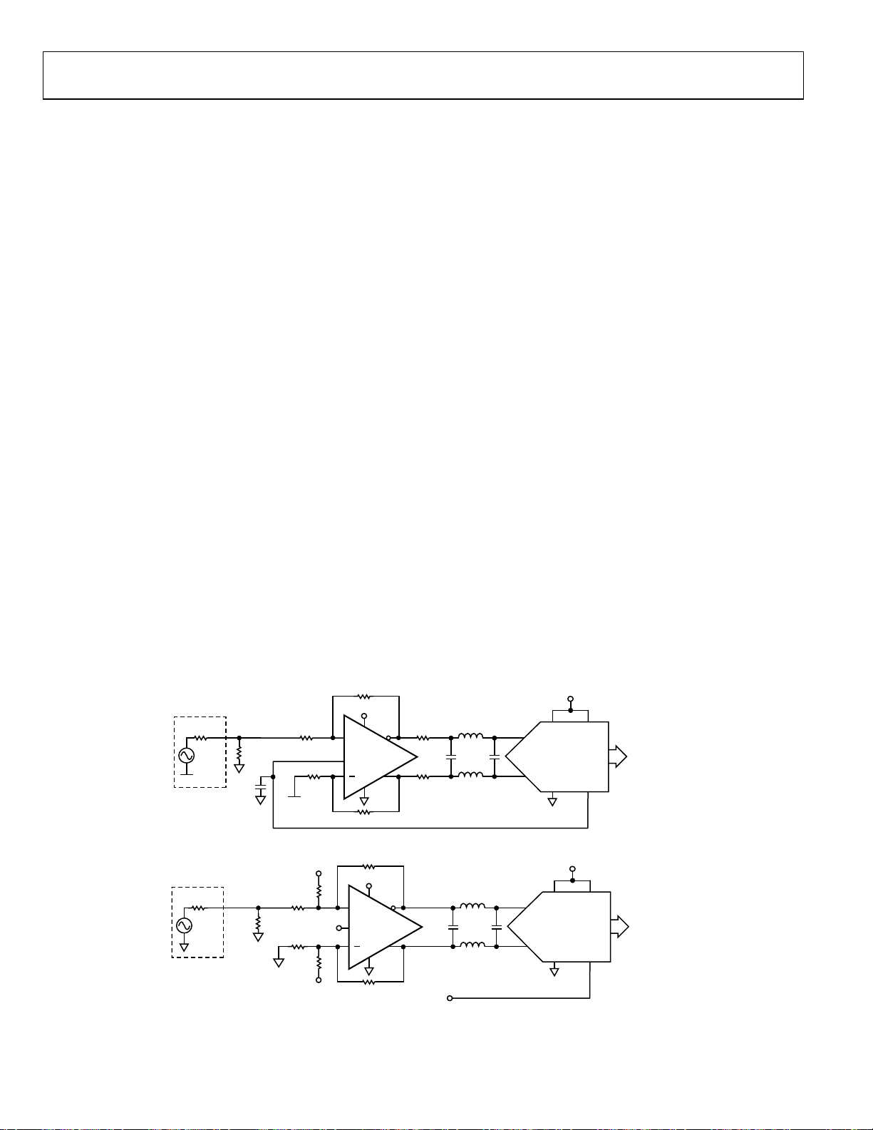
LAYOUT, GROUNDING, AND BYPASSING
The ADA4930-1/ADA4930-2 are high speed devices. Realizing
their superior performance requires attention to the details of
high speed PCB design.
The first requirement is to use a multilayer PCB with solid ground
and power planes that cover as much of the board area as possible.
Bypass each power supply pin directly to a nearby ground plane, as
close to the device as possible. Use 0.1 µF high frequency ceramic
chip capacitors.
Provide low frequency bulk bypassing, using 10 µF tantalum
capacitors from each supply to ground.
Stray transmission line capacitance in combination with package
parasitics can potentially form a resonant circuit at high frequencies,
resulting in excessive gain peaking or possible oscillation.
Signal routing should be short and direct to avoid such parasitic
effects. Provide symmetrical layout for complementary signals
to maximize balanced performance.
Use radio frequency transmission lines to connect the driver
and receiver to the amplifier.
Minimize stray capacitance at the input/output pins by clearing
the underlying ground and low impedance planes near these pins
(see Figure 56).
If the driver/receiver is more than one-eighth of the wavelength
from the amplifier, the signal trace widths should be minimal.
This nontransmission line configuration requires the underlying
and adjacent ground and low impedance planes to be cleared
near the signal lines.
The exposed thermal paddle is internally connected to the ground
pin of the amplifier. Solder the paddle to the low impedance
ground plane on the PCB to ensure the specified electrical
performance and to provide thermal relief. To reduce thermal
impedance further, it is recommended that the ground planes
on all layers under the paddle be connected together with vias.
1.30
0.80
1.30
0.80
9209-058
Figure 56. ADA4930-1 Ground and Power Plane Voiding
in the Vicinity of R
and RG
F
Figure 57. Recommended PCB Thermal Attach Pad Dimensions (Millimeters)
09209-059
1.3 mm
0.8 mm
TOP METAL
GROUND PLANE
POWER PLANE
BOTTOM M ETAL
Figure 58. Cross-Section of 4-Layer PCB Showing Thermal Via Connection to Buried Ground Plane (Dimensions in Millimeters)
09209-060
Rev. A | Page 23 of 28
ADA4930-1/ADA4930-2
HIGH PERFORMANCE ADC DRIVING
The ADA4930-1/ADA4930-2 provide excellent performance in
3.3 V single-supply applications.
The circuit shown in Figure 59 is an example of the ADA4930-1
driving an AD9255, 14-bit, 80 MSPS ADC that is specified to
operate with a single 1.8 V supply. The performance of the ADC
is optimized when it is driven differentially, making the best use of
the signal swing available within the 1.8 V supply. The ADA4930-1
performs the single-ended-to-differential conversion, commonmode level shifting, and buffering of the driving signal.
The ADA4930-1 is configured for a single-ended input to differential
output with a gain of 2 V/V. The 84.5 Ω termination resistor, in
parallel with the single-ended input impedance of 95.1 Ω, provides
a 50 Ω termination for the source. The additional 31.6 Ω (95 Ω
total) at the inverting input balances the parallel impedance of
the 50 Ω source and the termination resistor that drives the
noninverting input.
The V
pin is connected to the VCM output of the AD9255
OCM
and sets the output common mode of the ADA4930-1 at 1 V.
Note that a dc bias must be added to the signal source and its
Thevenin equivalent to the gain resistor on the inverting side
to ensure that the inputs of the ADA4930-1 are kept at or above
the specified minimum input common-mode voltage at all times.
The 0.5 V dc bias at the signal source and the 0.314 V dc bias on the
gain resistor at the inverting input set the inputs of the ADA4930-1
to ~0.48 V dc. With 1 V p-p maximum signal swing at the input,
the ADA4930-1 inputs swing between 0.36 V and 0.6 V.
For a common-mode voltage of 1 V, each ADA4930-1 output
swings between 0.501 V and 1.498 V, providing a 1.994 V p-p
differential output.
301
3.3V
63.4
0.314V
95
V
OCM
+
ADA4930-1
301
Figure 59. Driving an AD9255, 14-Bit, 80 MSPS ADC
OCM
301
3.3V
+
ADA4930-2
739
64.2
96.2
739
3.3V
V
0.5V
50
V
1V p-p
50
V
IN
1V p-p
84.5
IN
88.5
A third-order, 40 MHz, low-pass filter between the ADA4930-1
and the AD9255 reduces the noise bandwidth of the amplifier
and isolates the driver outputs from the ADC inputs.
The circuit shown in Figure 60 is an example of ½ of an
ADA4930-2 driving ½ of an AD9640, a 14-bit, 80 MSPS
ADC that is specified to operate with a single 1.8 V supply.
The performance of the ADC is optimized when it is driven
differentially, making the best use of the signal swing available
within the 1.8 V supply. The ADA4930-2 performs the singleended-to-differential conversion, common-mode level shifting,
and buffering of the driving signal.
The ADA4930-2 is configured for a single-ended input to differential
output with a gain of 2 V/V. The 88.5 Ω termination resistor, in
parallel with the single-ended input impedance of 114.75 Ω,
provides a 50 Ω termination for the source. The increased gain
resistance at the inverting input balances the 50 Ω source resistance
and the termination resistor that drives the noninverting input.
The V
pin is connected to the CML output of the AD9640 and
OCM
sets the output common mode of the ADA4930-2 at 1 V.
The 739 Ω resistors between each input and the 3.3 V supply
provide the necessary dc bias to guarantee compliance with the
input common-mode range of the ADA4930-2.
For a common-mode voltage of 1 V, each ADA4930-2 output
swings between 0.501 V and 1.498 V, providing a 1.994 V p-p
differential output.
A third-order, 40 MHz, low-pass filter between the ADA4930-2
and the AD9640 reduces the noise bandwidth of the amplifier
and isolates the driver outputs from the ADC inputs.
1.8V
33
33
168nH
90pF30pF
168nH
168nH
90pF30pF
168nH
VIN–
VIN+
AGND VCM
VIN–
VIN+
AGND CML
DRVDDAVDD
AD9255
1.8V
DRVDDAVDD
AD9640
D11 TO
D0
D11 TO
D0
09209-157
3.3V
301
V
OCM
09209-158
Figure 60. Driving an AD9640, 14-Bit, 80 MSPS ADC
Rev. A | Page 24 of 28

ADA4930-1/ADA4930-2
OUTLINE DIMENSIONS
0.50
0.40
0.30
16
1
(BOTTOM VIEW)
EXPOSED
PAD
4
5
EXPOSED
PAD
(BOTTOM VIEW)
2.50 BCS
FOR PROPER CONNECTION OF
THE EXPOSED PAD, REFER TO
THE PIN CONFIGURATION AND
FUNCTION DESCRIPTIONS
SECTION OF THIS DATA SHEET.
PIN 1
INDICATOR
*
1.45
1.30 SQ
1.15
0.25 MIN
P
N
I
N
I
D
1
24
2.44
2.34 SQ
2.24
6
7
0.20 MIN
072208-A
1
A
R
O
T
C
I
PIN 1
INDICATOR
1.00
0.85
0.80
SEATING
PLANE
PIN 1
INDICATOR
0.90
0.85
0.80
SEATING
PLANE
12° MAX
3.00
BSC SQ
TOP
VIEW
0.30
0.23
0.18
*
COMPLIANT
EXCEPT FOR EXPOSED PAD DIMENSION.
2.75
BSC SQ
0.80 MAX
0.65 TYP
0.05 MAX
0.02 NOM
0.20 REF
TO
JEDEC STANDARDS MO-220-VEED-2
0.45
0.50
BSC
1.50 REF
0.60 MAX
13
12
9
8
FOR PROPER CONNECTION O F
THE EXPOSED PAD, REFER TO
THE PIN CONF IGURATIO N AND
FUNCTION DESCRIPTIONS
SECTION OF THIS DATA SHEET.
Figure 61. 16-Lead Lead Frame Chip Scale Package [LFCSP_VQ]
3 mm × 3 mm Body, Very Thin Quad
(CP-16-2)
Dimensions shown in millimeters
12° MAX
4.10
4.00 SQ
3.90
TOP VIEW
0.70 MAX
0.65 TYP
0.30
0.23
0.18
3.75 BSC
SQ
0.20 REF
0.60 MAX
0.05 MAX
0.02 NOM
COPLANARITY
0.05
0.50
BSC
0.50
0.40
0.30
0.60 MAX
18
13
12
19
COMPLIANTTOJEDEC STANDARDS MO-220-VGGD-8
08-18-2010-A
Figure 62. 24-Lead Lead Frame Chip Scale Package [LFCSP_VQ]
4 mm × 4 mm Body, Very Thin Quad
(CP-24-13)
Dimensions shown in millimeters
ORDERING GUIDE
Model1 Temperature Range Package Description Package Option Ordering Quantity Branding
ADA4930-1YCPZ-R2 −40°C to +105°C 16-Lead LFCSP_VQ CP-16-2 250 H1G
ADA4930-1YCPZ-RL −40°C to +105°C 16-Lead LFCSP_VQ CP-16-2 5,000 H1G
ADA4930-1YCPZ-R7 −40°C to +105°C 16-Lead LFCSP_VQ CP-16-2 1,500 H1G
ADA4930-1YCP-EBZ Evaluation Board
ADA4930-2YCPZ-R2 −40°C to +105°C 24-Lead LFCSP_VQ CP-24-13 250
ADA4930-2YCPZ-RL −40°C to +105°C 24-Lead LFCSP_VQ CP-24-13 5,000
ADA4930-2YCPZ-R7 −40°C to +105°C 24-Lead LFCSP_VQ CP-24-13 1,500
ADA4930-2YCP-EBZ Evaluation Board
1
Z = RoHS Compliant Part.
Rev. A | Page 25 of 28

ADA4930-1/ADA4930-2
NOTES
Rev. A | Page 26 of 28

ADA4930-1/ADA4930-2
NOTES
Rev. A | Page 27 of 28

ADA4930-1/ADA4930-2
NOTES
©2010 Analog Devices, Inc. All rights reserved. Trademarks and
registered trademarks are the property of their respective owners.
D09209-0-10/10(A)
Rev. A | Page 28 of 28
 Loading...