

Page 1
Ultralow Distortion
–
Current Feedback Differential ADC Driver
FEATURES
Extremely low harmonic distortion
−105 dBc HD2 @ 10 MHz
−91 dBc HD2 @ 70 MHz
−87 dBc HD2 @ 100 MHz
−103 dBc HD3 @ 10 MHz
−98 dBc HD3 @ 70 MHz
−89 dBc HD3 @ 100 MHz
Better distortion at higher gains than VF amplifiers
Low input voltage noise: 1.4 nV/√Hz
High speed
−3 dB bandwidth of 2.3 GHz
0.1 dB gain flatness: 150 MHz
Slew rate: 5000 V/μs, 25% to 75%
Fast 0.1% settling time: 10 ns
Low input offset voltage: 0.3 mV typical
Externally adjustable gain
Stability and bandwidth controlled by feedback resistor
Differential-to-differential or single-ended-to-differential
operation
Adjustable output common-mode voltage
Wide supply operation: +5 V to ±5 V
APPLICATIONS
ADC drivers
Single-ended-to-differential converters
IF and baseband gain blocks
Differential buffers
Differential line drivers
GENERAL DESCRIPTION
The ADA4927 is a low noise, ultralow distortion, high speed,
current feedback differential amplifier that is an ideal choice for
driving high performance ADCs with resolutions up to 16 bits
from dc to 100 MHz. The output common-mode level can easily be
matched to the required ADC input common-mode levels. The
internal common-mode feedback loop provides exceptional output
balance and suppression of even-order distortion products.
Differential gain configurations are easily realized using an
external feedback network comprising four resistors. The
current feedback architecture provides loop gain that is nearly
independent of closed-loop gain, achieving wide bandwidth,
low distortion, and low noise at higher gains and lower power
consumption than comparable voltage feedback amplifiers.
The ADA4927 is fabricated using the Analog Devices, Inc., silicongermanium complementary bipolar process, enabling very low
levels of distortion with an input voltage noise of only 1.3 nV/√Hz.
Rev. A
Information furnished by Analog Devices is believed to be accurate and reliable. However, no
responsibility is assumed by Analog Devices for its use, nor for any infringements of patents or other
rights of third parties that may result from its use. Specifications subject to change without notice. No
license is granted by implication or otherwise under any patent or patent rights of Analog Devices.
Trademarks and registered trademarks are the property of their respective owners.
ADA4927-1/ADA4927-2
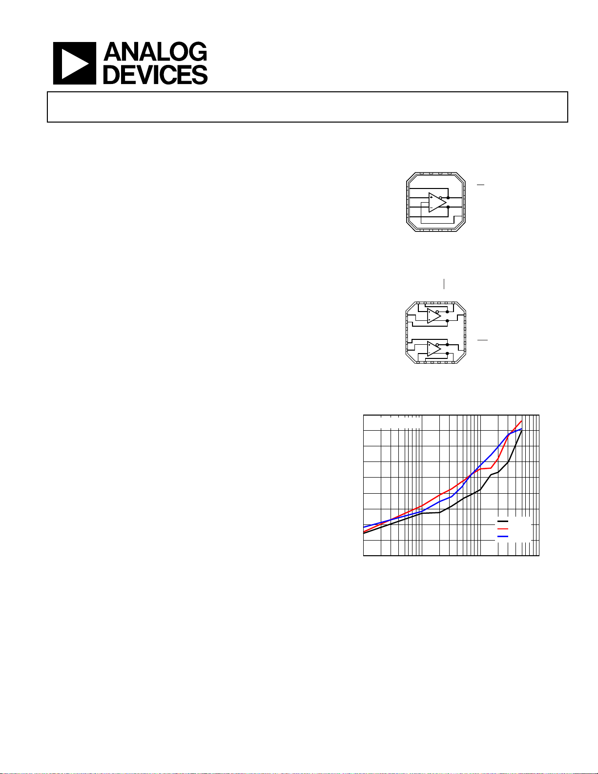
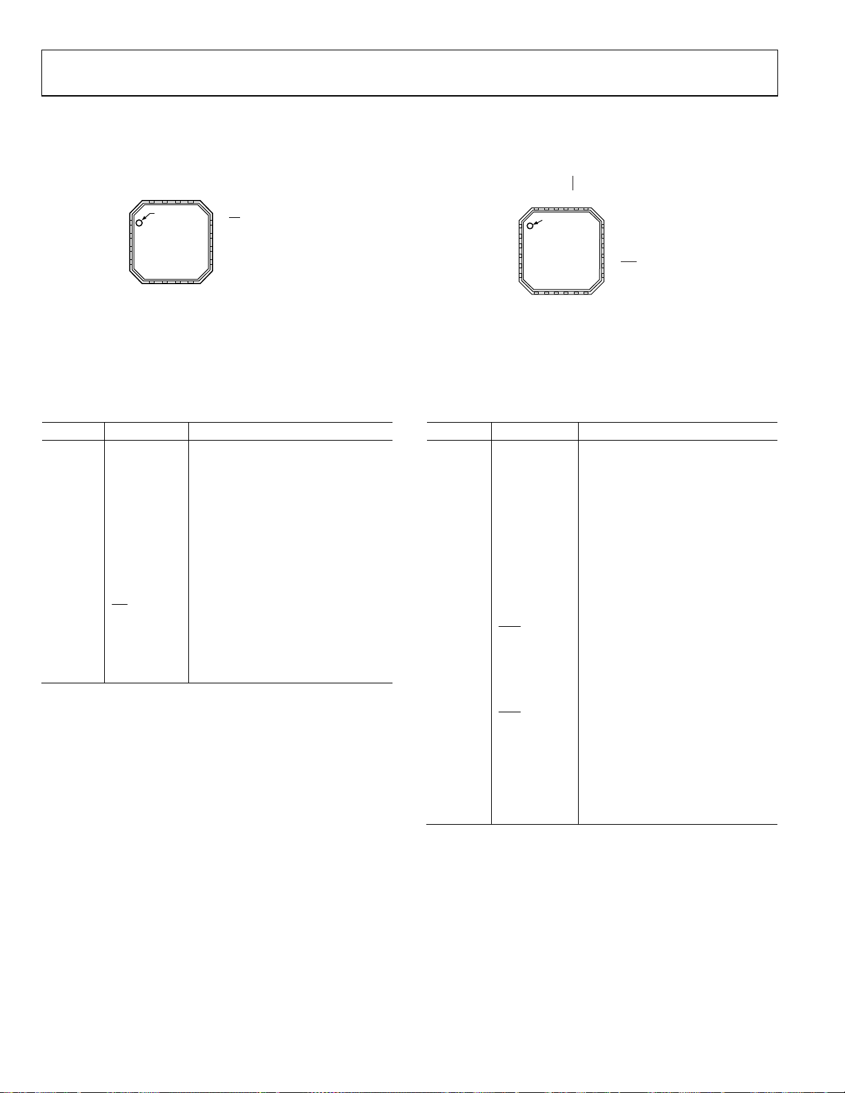
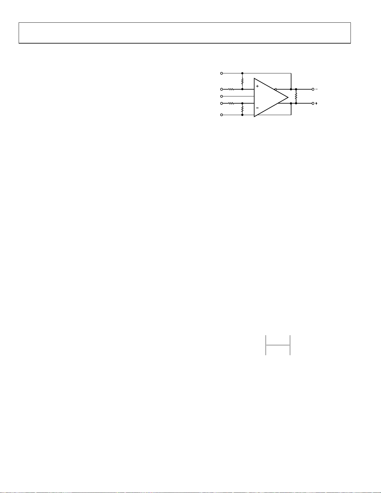
FUNCTIONAL BLOCK DIAGRAMS
1–FB
2+IN
3–IN
4+FB
1–IN1
2+FB1
3+V
S1
4+V
S1
5–FB2
6+IN2
40
V
= 2V p-p
OUT, dm
–50
–60
–70
–80
–90
–100
–110
–120
SPURIOUS-FREE DYNAMIC RANGE (dBc)
–130
1 10 100 1k
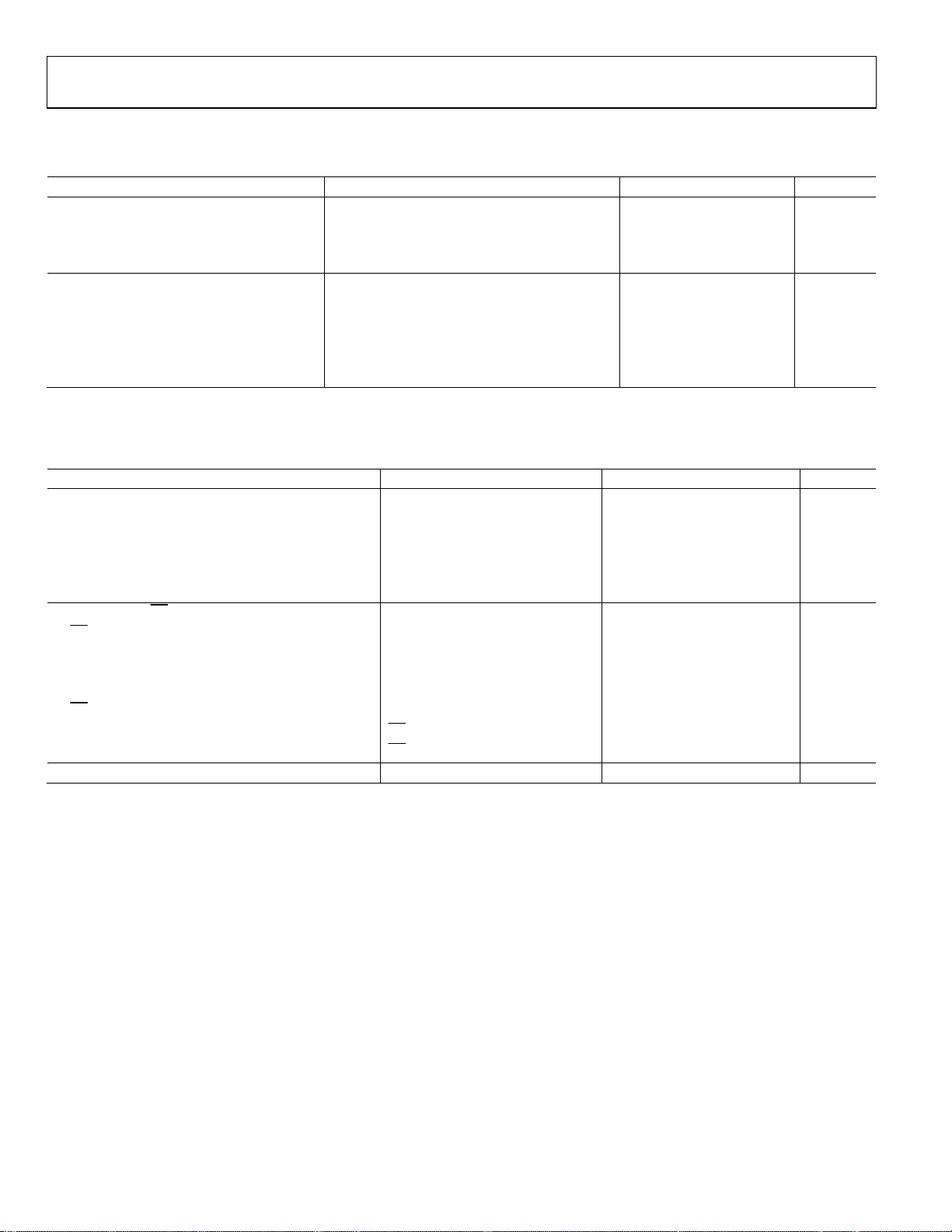
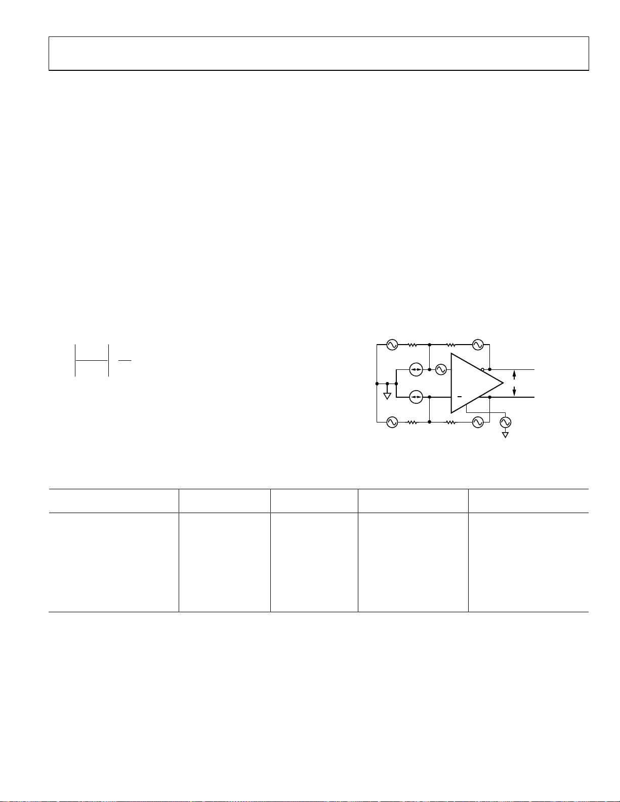
Figure 3. Spurious-Free Dynamic Range vs. Frequency at Various Gains
The low dc offset and excellent dynamic performance of the
ADA4927 make it well suited for a wide variety of data acquisition
and signal processing applications.
The ADA4927-1 is available in a Pb-free, 3 mm × 3 mm 16-lead
LFCSP, and the ADA4927-2 is available in a Pb-free, 4 mm × 4 mm
24-lead LFCSP. The pinouts are optimized to facilitate printed
circuit board (PCB) layout and to minimize distortion. They are
specified to operate over the −40°C to +105°C temperature range.
One Technology 62-9106, U.S.A.
Tel: 781.329.4700 www.analog.com
Fax: 781.461.3113 l rights reserved.
Way, P.O. Box 9106, Norwood, MA 020
©2008-2009 Analog Devices, Inc. Al
S
S
S
–V
–V
–V
–V
14
13
15
16
ADA4927-1
8
7
5
6
S
S
S
+V
+V
+V
+V
Figure 1.
S1
S1
–V
–V
–FB1
+IN1
24
PD1
20
21
22
23
ADA4927-2
9
7
8
11
10
S2
S2
–IN2
+V
+V
OCM2
+FB2
V
Figure 2.
FREQUENCY (MHz)
S
S
–OUT1
19
12
+OUT2
12 PD
11 –OUT
10 +OUT
9V
OCM
18 + OUT1
17 V
OCM1
16 – V
S2
–V
15
S2
14
PD2
13 –O UT2
07574-001
07574-002
G = 1
G = 10
G = 20
07574-026
Page 2

ADA4927-1/ADA4927-2
TABLE OF CONTENTS
Features .............................................................................................. 1
Applications ....................................................................................... 1
General Description ......................................................................... 1
Functional Block Diagrams ............................................................. 1
Revision History ............................................................................... 2
Specifications ..................................................................................... 3
±5 V Operation ............................................................................. 3
+5 V Operation ............................................................................. 5
Absolute Maximum Ratings ............................................................ 7
Thermal Resistance ...................................................................... 7
Maximum Power Dissipation ..................................................... 7
ESD Caution .................................................................................. 7
Pin Configurations and Function Descriptions ........................... 8
Typical Performance Characteristics ............................................. 9
Test Circuits ..................................................................................... 15
Theory of Operation ...................................................................... 16
Definition of Terms .................................................................... 16
Applications Information .............................................................. 17
Analyzing an Application Circuit ............................................ 17
Setting the Closed-Loop Gain .................................................. 17
Estimating the Output Noise Voltage ...................................... 17
Impact of Mismatches in the Feedback Networks ................. 18
Calculating the Input Impedance for an Application Circuit
....................................................................................................... 18
Input Common-Mode Voltage Range ..................................... 20
Input and Output Capacitive AC Coupling ............................ 20
Setting the Output Common-Mode Voltage .......................... 20
Power-Down ............................................................................... 21
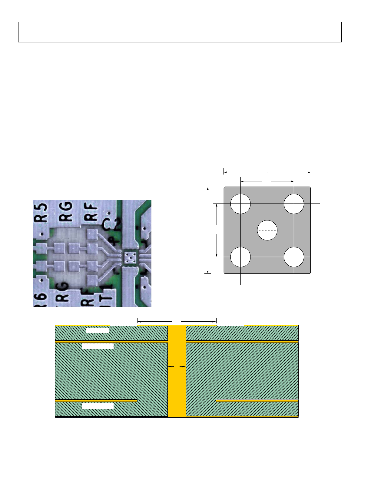
Layout, Grounding, and Bypassing .............................................. 22
High Performance ADC Driving ................................................. 23
Outline Dimensions ....................................................................... 24
Ordering Guide .......................................................................... 24
REVISION HISTORY
8/09—Rev. 0 to Rev. A
Changes to Ordering Guide .......................................................... 24
10/08—Revision 0: Initial Version
Rev. A | Page 2 of 24
Page 3

ADA4927-1/ADA4927-2
SPECIFICATIONS
±5 V OPERATION
TA = 25°C, +VS = 5 V, −VS = − 5 V, V
All specifications refer to single-ended input and differential outputs, unless otherwise noted. Refer to Figure 46 for signal definitions.
±DIN to V
Performance
OUT, dm
Table 1.
Parameter Conditions Min Typ Max Unit
DYNAMIC PERFORMANCE
−3 dB Small Signal Bandwidth V
−3 dB Large Signal Bandwidth V
Bandwidth for 0.1 dB Flatness V
V
Slew Rate V
Settling Time to 0.1% V
Overdrive Recovery Time VIN = 0 V to 0.9 V step, G = 10 10 ns
NOISE/HARMONIC PERFORMANCE See Figure 45 for distortion test circuit
Second Harmonic V
V
V
Third Harmonic V
V
V
IMD f1 = 70 MHz, f2 = 70.1 MHz, V
f
Voltage Noise (RTI) f = 100 kHz, G = 28 1.4 nV/√Hz
Input Current Noise f = 100 kHz, G = 28 14 pA/√Hz
Crosstalk f = 100 MHz, ADA4927-2 −75 dB
INPUT CHARACTERISTICS
Offset Voltage VIP = VIN = V
t
Input Bias Current −15 +0.5 +15 µA
t
Input Offset Current −10.5 −0.6 +10.5 µA
Input Resistance Differential 14 Ω
Common mode 120 kΩ
Input Capacitance Differential 0.5 pF
Input Common-Mode Voltage Range −3.5 +3.5 V
CMRR V
Open-Loop Transresistance DC 120 185 kΩ
OUTPUT CHARACTERISTICS
Output Voltage Swing Each single-ended output, RF = RG = 10 kΩ −3.8 +3.8 V
Linear Output Current 65 mA p-p
Output Balance Error
= 0 V, RF = 301 , RG = 301 , RT = 56.2 (when used), R
OCM
= 0.1 V p-p 2300 MHz
OUT, dm
= 2.0 V p-p 1500 MHz
OUT, dm
= 0.1 V p-p, ADA4927-1 150 MHz
OUT, dm
= 0.1 V p-p, ADA4927-2 120 MHz
OUT, dm
= 2 V step, 25% to 75% 5000 V/µs
OUT, dm
= 2 V step 10 ns
OUT, dm
= 2 V p-p, 10 MHz −105 dBc
OUT, dm
= 2 V p-p, 70 MHz −91 dBc
OUT, dm
= 2 V p-p, 100 MHz −87 dBc
OUT, dm
= 2 V p-p, 10 MHz −103 dBc
OUT, dm
= 2 V p-p, 70 MHz −98 dBc
OUT, dm
= 2 V p-p, 100 MHz −89 dBc
OUT, dm
= 2 V p-p −94 dBc
OUT, dm
= 140 MHz, f2 = 140.1 MHz, V
1
= 0 V −1.3 +0.3 +1.3 mV
OCM
to t
MIN
MIN
V
variation ±1.5 µV/°C
MAX
to t
variation ±0.1 µA/°C
MAX
/V
, V
OUT, dm
OUT, cm
/V
IN, cm
OUT, dm
= ±1 V −70 −93 dB
IN, cm
, V
OUT, dm
= 1 V, 10 MHz,
= 2 V p-p −85 dBc
OUT, dm
see Figure 44 for test circuit
= 1 kΩ, unless otherwise noted.
L, dm
−65 dB
Rev. A | Page 3 of 24
Page 4
ADA4927-1/ADA4927-2
V
to V
OCM
Table 2.
Parameter Conditions Min Typ Max Unit
V
DYNAMIC PERFORMANCE
OCM
Small Signal −3 dB Bandwidth V
Slew Rate VIN = −1.0 V to +1.0 V, 25% to 75% 1000 V/µs
Input Voltage Noise (RTI) f = 100 kHz 15 nV/√Hz
V
INPUT CHARACTERISTICS
OCM
Input Voltage Range ±3.5 V
Input Resistance 3.8 5.0 7.5 kΩ
Input Offset Voltage V
V
CMRR ∆V
OCM
Gain ∆V
General Performance
Table 3.
Parameter Conditions Min Typ Max Unit
POWER SUPPLY
Operating Range 4.5 11.0 V
Quiescent Current per Amplifier 20.0 22.1 mA
t
Powered down 2.4 mA
Power Supply Rejection Ratio ∆V
POWER-DOWN (PD)
PD Input Voltage
Enabled >3.2 V
Turn-Off Time To 0.1% 15 µs
Turn-On Time To 0.1% 400 ns
PD Pin Bias Current per Amplifier
Enabled
Disabled
OPERATING TEMPERATURE RANGE −40 +105 °C
Performance
OUT, cm
= 100 mV p-p 1300 MHz
OUT, cm
OS, cm
OUT, dm
OUT, cm
= V
OUT, cm
/∆V
/∆V
, V
= V
DIN+
, ∆V
OCM
OCM
, ∆V
OCM
OCM
to t
MIN
MAX
/∆VS, ∆VS = 1 V −70 −89 dB
OUT, dm
= +VS/2 −10 −2 +5.2 mV
DIN−
= ±1 V −70 −97 dB
= ±1 V 0.90 0.97 1.00 V/V
variation ±9.0 µA/°C
Powered down <1.8 V
PD
PD
= 5 V
= 0 V
−2 +2 µA
−110 −90 µA
Rev. A | Page 4 of 24
Page 5

ADA4927-1/ADA4927-2
+5 V OPERATION
TA = 25°C, +VS = 5 V, −VS = 0 V, V
All specifications refer to single-ended input and differential outputs, unless otherwise noted. Refer to Figure 46 for signal definitions.
±DIN to V
Performance
OUT, dm
Table 4.
Parameter Conditions Min Typ Max Unit
DYNAMIC PERFORMANCE
−3 dB Small Signal Bandwidth V
−3 dB Large Signal Bandwidth V
Bandwidth for 0.1 dB Flatness V
V
Slew Rate V
Settling Time to 0.1% V
Overdrive Recovery Time VIN = 0 V to 0.15 V step, G = 10 10 ns
NOISE/HARMONIC PERFORMANCE See Figure 45 for distortion test circuit
Second Harmonic V
V
V
Third Harmonic V
V
V
IMD f1 = 70 MHz, f2 = 70.1 MHz, V
f
Voltage Noise (RTI) f = 100 kHz, G = 28 1.4 nV/√Hz
Input Current Noise f = 100 kHz, G = 28 19 pA/√Hz
Crosstalk f = 100 MHz, ADA4927-2 −75 dB
INPUT CHARACTERISTICS
Offset Voltage VIP = VIN = V
t
Input Bias Current −30 −12 +4.0 µA
t
Input Offset Current −10.5 −0.8 +10.5 µA
Input Resistance Differential 14 Ω
Common mode 120 kΩ
Input Capacitance Differential 0.5 pF
Input Common-Mode Voltage Range 1.3 3.7 V
CMRR V
Open-Loop Transresistance DC 120 185 kΩ
OUTPUT CHARACTERISTICS
Output Voltage Swing Each single-ended output +1.0 +4.0 V
Linear Output Current 50 mA p-p
Output Balance Error
= 2.5 V, RF = 301 , RG = 301 , RT = 56.2 (when used), R
OCM
= 0.1 V p-p 2000 MHz
OUT, dm
= 2.0 V p-p 1300 MHz
OUT, dm
= 0.1 V p-p, ADA4927-1 150 MHz
OUT, dm
= 0.1 V p-p, ADA4927-2 110 MHz
OUT, dm
= 2 V step, 25% to 75% 4200 V/µs
OUT, dm
= 2 V step 10 ns
OUT, dm
= 2 V p-p, 10 MHz −104 dBc
OUT, dm
= 2 V p-p, 70 MHz −91 dBc
OUT, dm
= 2 V p-p, 100 MHz −86 dBc
OUT, dm
= 2 V p-p, 10 MHz −95 dBc
OUT, dm
= 2 V p-p, 70 MHz −80 dBc
OUT, dm
= 2 V p-p, 100 MHz −76 dBc
OUT, dm
= 2 V p-p −93 dBc
OUT, dm
= 140 MHz, f2 = 140.1 MHz, V
1
= 0 V −1.3 +0.3 +1.3 mV
OCM
to t
MIN
MIN
V
variation ±1.5 µV/°C
MAX
to t
variation ±0.12 µA/°C
MAX
/V
, V
OUT, dm
OUT, cm
/V
IN, cm
OUT, dm
= ±1 V −70 −96 dB
IN, cm
, V
OUT, dm
= 1 V, 10 MHz,
= 2 V p-p −84 dBc
OUT, dm
see Figure 44 for test circuit
= 1 kΩ, unless otherwise noted.
L, dm
−65 dB
Rev. A | Page 5 of 24
Page 6
ADA4927-1/ADA4927-2
V
to V
OCM
Table 5.
Parameter Conditions Min Typ Max Unit
V
DYNAMIC PERFORMANCE
OCM
Small signal −3 dB Bandwidth V
Slew Rate VIN = 1.5 V to 3.5 V, 25% to 75% 1000 V/µs
Input Voltage Noise (RTI) f = 100 kHz 15 nV/√Hz
V
INPUT CHARACTERISTICS
OCM
Input Voltage Range 1.5 to 3.5 V
Input Resistance 3.8 5.0 7.5 kΩ
Input Offset Voltage V
V
CMRR ∆V
OCM
Gain ∆V
General Performance
Table 6.
Parameter Conditions Min Typ Max Unit
POWER SUPPLY
Operating Range 4.5 11.0 V
Quiescent Current per Amplifier 20 21.6 mA
t
Powered down 0.6 mA
Power Supply Rejection Ratio ∆V
POWER-DOWN (PD)
PD Input Voltage
Enabled >3.0 V
Turn-Off Time 20 s
Turn-On Time 500 ns
PD Pin Bias Current per Amplifier
Enabled
Disabled
OPERATING TEMPERATURE RANGE −40 +105 °C
Performance
OUT, cm
= 100 mV p-p 1300 MHz
OUT, cm
OS, cm
OUT, dm
OUT, cm
= V
OUT, cm
/∆V
/∆V
, V
= V
= +VS/2 −5.0 +2.0 +10 mV
DIN−
= ±1 V −70 −100 dB
= ±1 V 0.90 0.97 1.00 V/V
variation ±7.0 µA/°C
/∆VS, ∆VS = 1 V −70 −89 dB
OCM
OCM
MIN
DIN+
, ∆V
, ∆V
to t
OUT, dm
OCM
OCM
MAX
Powered down <1.7 V
PD
PD
= 5 V
= 0 V
−2 +2 µA
−105 −95 µA
Rev. A | Page 6 of 24
Page 7
ADA4927-1/ADA4927-2
ABSOLUTE MAXIMUM RATINGS
Table 7.
Parameter Rating
Supply Voltage 11 V
Power Dissipation See Figure 4
Input Currents +IN, −IN,
PD
±5 mA
Storage Temperature Range −65°C to +125°C
Operating Temperature Range −40°C to +105°C
Lead Temperature (Soldering, 10 sec) 300°C
Junction Temperature 150°C
Stresses above those listed under Absolute Maximum Ratings
may cause permanent damage to the device. This is a stress
rating only; functional operation of the device at these or any
other conditions above those indicated in the operational
section of this specification is not implied. Exposure to absolute
maximum rating conditions for extended periods may affect
device reliability.
THERMAL RESISTANCE
θJA is specified for the device (including exposed pad) soldered
to a high thermal conductivity 2s2p circuit board, as described
in EIA/JESD 51-7.
Table 8.
Package Type θJA Unit
16-Lead LFCSP (Exposed Pad) 87 °C/W
24-Lead LFCSP (Exposed Pad) 47 °C/W
MAXIMUM POWER DISSIPATION
The maximum safe power dissipation in the ADA4927 package
is limited by the associated rise in junction temperature (T
the die. At approximately 150°C, which is the glass transition
temperature, the plastic changes its properties. Even temporarily
exceeding this temperature limit can change the stresses that the
package exerts on the die, permanently shifting the parametric
performance of the ADA4927. Exceeding a junction temperature
of 150°C for an extended period can result in changes in the
silicon devices, potentially causing failure.
) on
J
The power dissipated in the package (P
quiescent power dissipation and the power dissipated in the
package due to the load drive. The quiescent power is the voltage
between the supply pins (V
) times the quiescent current (IS).
S
The power dissipated due to the load drive depends upon the
particular application. The power due to load drive is calculated
by multiplying the load current by the associated voltage drop
across the device. RMS voltages and currents must be used in
these calculations.
Airflow increases heat dissipation, effectively reducing θ
addition, more metal directly in contact with the package leads/
exposed pad from metal traces, throughholes, ground, and power
planes reduces θ
.
JA
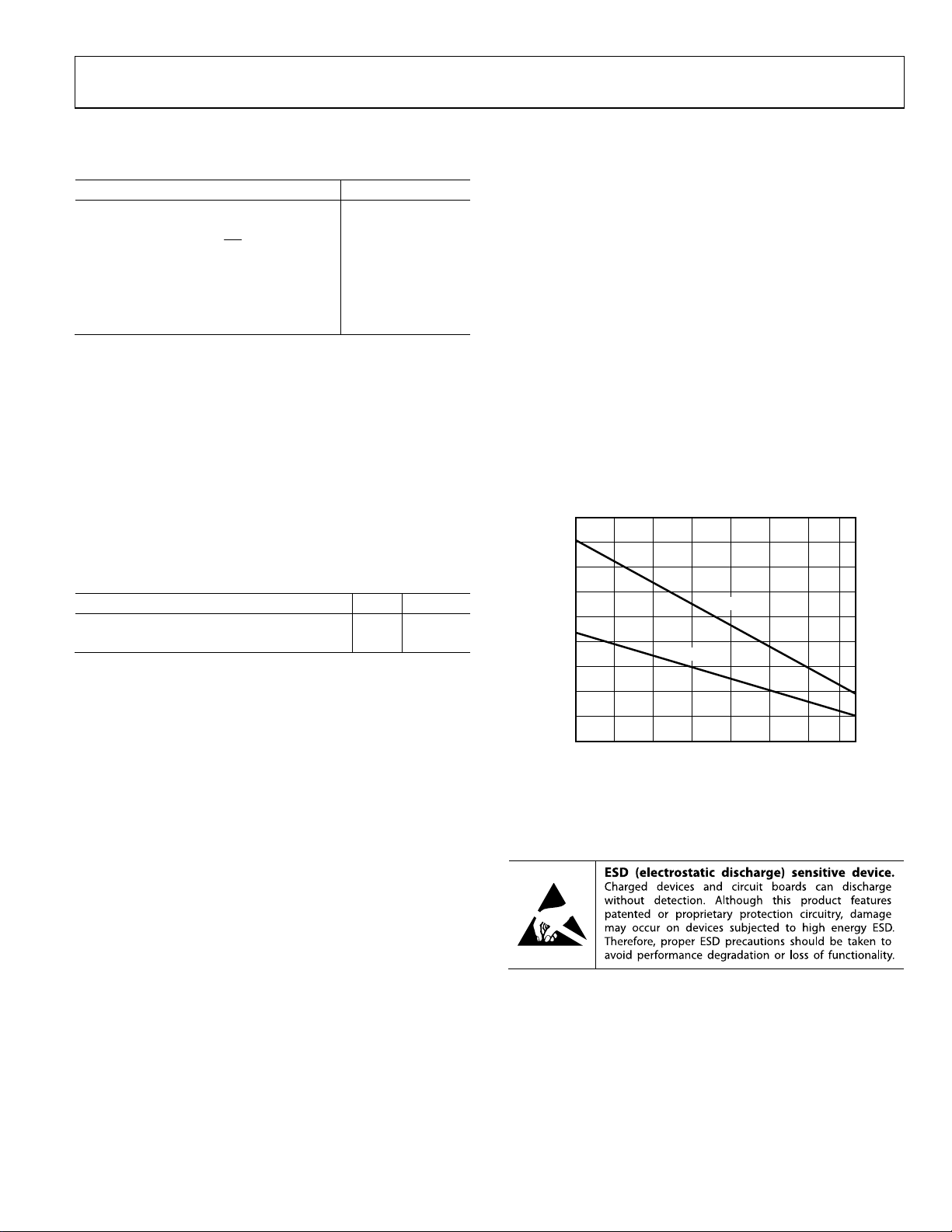
Figure 4 shows the maximum safe power dissipation in the package
vs. the ambient temperature for the single 16-lead LFCSP (87°C/W)
and the dual 24-lead LFCSP (47°C/W) on a JEDEC standard
4-layer board with the exposed pad soldered to a PCB pad that
is connected to a solid plane.
4.5
4.0
3.5
3.0
2.5
2.0
1.5
1.0
MAXIMUM POWER DISSIPATION (W)
0.5
0
–40 –20 0 20 40
AMBIENT TEMPERATURE (°C)
Figure 4. Maximum Power Dissipation vs.
Ambient Temperature for a 4-Layer Board
ADA4927-2
ADA4927-1
ESD CAUTION
) is the sum of the
D
60 80 100
JA
. In
07574-003
Rev. A | Page 7 of 24
Page 8
ADA4927-1/ADA4927-2
+
–
PIN CONFIGURATIONS AND FUNCTION DESCRIPTIONS
S
S
S
S
–V
–V
–V
–V
14
13
15
16
PIN 1
INDICATO R
1–FB
2+IN
ADA4927-1
TOP VIEW
3–IN
(Not to Scale)
4+FB
5
6
S
S
+V
+V
NOTES
1. CONNECT THE EXPOSED PADDLE TO ANY PLANE
BETWEEN AND INCL UDING +V
Figure 5. ADA4927-1 Pin Configuration
12 PD
11 –OUT
10 +OUT
9V
OCM
8
7
S
S
+V
+V
AND –VS.
S
07574-005
1
–IN1
FB1
2
+V
3
S1
+V
4
S1
FB2
5
+IN2
6
NOTES
1. CONNECT THE EX POSED PADDLE T O ANY PLANE
BETWEEN AND INCL UDING +V
Figure 6. ADA4927-2 Pin Configuration
–VS1–VS1–FB1
+IN1
20
21
22
23
24
PIN 1
INDICATOR
ADA4927-2
TOP VIEW
(Not to Scale)
9
7
8
11
10
S2
S2
B2
–IN2
+V
+V
+F
V
PD1
–OUT1
19
+OUT1
18
V
17
OCM1
–V
16
S2
–V
15
S2
14
PD2
–OUT2
13
12
OCM2
+OUT2
AND –VS.
S
7574-006
Table 9. ADA4927-1 Pin Function Descriptions
Pin No. Mnemonic Description
1 −FB
Negative Output for Feedback
Component Connection
2 +IN Positive Input Summing Node
3 −IN Negative Input Summing Node
4 +FB
Positive Output for Feedback
Component Connection
5 to 8 +VS Positive Supply Voltage
9 V
Output Common-Mode Voltage
OCM
10 +OUT Positive Output for Load Connection
11 −OUT Negative Output for Load Connection
12
PD
Power-Down Pin
13 to 16 −VS Negative Supply Voltage
17 (EPAD)
Exposed
Pad (EPAD)
Connect the exposed pad to any
plane between and including
and −VS.
+V
S
Table 10. ADA4927-2 Pin Function Descriptions
Pin No. Mnemonic Description
1 −IN1 Negative Input Summing Node 1
2 +FB1 Positive Output Feedback 1
3, 4 +V
5 −FB2
6 +IN2
7 −IN2
8 +FB2
9, 10 +V
11 V
12 +OUT2
13 −OUT2
14
15, 16 −V
17 V
Positive Supply Voltage 1
S1
Negative Output Feedback 2
Positive Input Summing Node 2
Negative Input Summing Node 2
Positive Output Feedback 2
Positive Supply Voltage 2
S2
Output Common-Mode Voltage 2
OCM2
Positive Output 2
Negative Output 2
PD2
Negative Supply Voltage 2
S2
Output Common-Mode Voltage 1
OCM1
Power-Down Pin 2
18 +OUT1 Positive Output 1
19 −OUT1
20
21, 22 −V
PD1
Negative Supply Voltage 1
S1
23 −FB1
24 +IN1
25 (EPAD)
Exposed
Pad (EPAD)
Negative Output 1
Power-Down Pin 1
Negative Output Feedback 1
Positive Input Summing Node 1
Connect the exposed pad to any
plane between and including
+VS and −VS.
Rev. A | Page 8 of 24
Page 9
ADA4927-1/ADA4927-2
TYPICAL PERFORMANCE CHARACTERISTICS
TA = 25°C, +VS = 5 V, −VS = −5 V, V
Refer to Figure 43 for basic test setup. Refer to Figure 46 for signal definitions.
3
V
= 100mV p-p
OUT,dm
= 0 V, RG = 301 , RF = 301 , RT = 56.2 Ω (when used), R
OCM
3
V
OUT,dm
= 2V p-p
= 1 kΩ, unless otherwise noted.
L, dm
0
–3
–6
–9
G = 1, RF = 301Ω
NORMALIZE D CLOSED-LO OP GAIN (d B)
–12
G = 10, RF = 442Ω
G = 20, RF = 604Ω
1 10 100 1k 10k
FREQUENCY (MHz )
Figure 7. Small Signal Frequency Response for Various Gains
3
V
= 100mV p-p
OUT,dm
0
–3
CLOSED-LOOP GAIN (dB)
–6
VS = ±5V
= ±2.5V
V
S
–9
1 10 100 1k 10k
FREQUENCY (MHz)
Figure 8. Small Signal Frequency Response for Various Supplies
3
V
= 100mV p-p
OUT,dm
0
–3
–6
–9
NORMALIZE D CLOSED-LO OP GAIN (d B)
–12
07574-007
G = 1, RF = 301Ω
G = 10, RF = 442Ω
G = 20, RF = 604Ω
1 10 100 1k 10k
FREQUENCY (MHz )
07574-010
Figure 10. Large Signal Frequency Response for Various Gains
3
V
= 2V p-p
OUT,dm
0
–3
CLOSED-LOOP GAIN (dB)
–6
–9
07574-008
VS = ±5V
= ±2.5V
V
S
10 100 1k 10k
FREQUENCY (MHz)
07574-011
Figure 11. Large Signal Frequency Response for Various Supplies
3
V
= 2V p-p
OUT,dm
0
–3
–6
CLOSED-LOOP GAIN (dB)
–9
–12
TA +25°C
T
+105°C
A
T
–40°C
A
1 10 100 1k 10k
FREQUENCY (MHz )
Figure 9. Small Signal Frequency Response for Various Temperatures
07574-009
Rev. A | Page 9 of 24
0
–3
–6
CLOSED-LOOP GAIN (dB)
–12
TA +25°C
–9
T
+105°C
A
T
–40°C
A
1 10 100 1k 10k
FREQUENCY (MHz )
Figure 12. Large Signal Frequency Response for Various Temperatures
07574-012
Page 10

ADA4927-1/ADA4927-2
3
V
= 100mV p-p V
OUT,dm
3
OUT,dm
= 2V p-p
0
–3
–6
CLOSED-LOOP GAIN (dB)
–9
–12
RL = 200Ω
R
= 1kΩ
L
1 10 100 1k 10k
FREQUENCY (MHz )
Figure 13. Small Signal Frequency Response for Various Loads
3
V
= 100mV p-p
OUT,dm
0
–3
–6
V
= –4V
OCM
V
= –3.5V
CLOSED-LOOP GAIN (dB)
–9
–12
1 10 100 1k 10k
OCM
V
= 0V
OCM
V
= +3.5V
OCM
V
= +4V
OCM
FREQUENCY (MHz )
0
–3
–6
CLOSED-LOOP GAIN (dB)
–9
4-013
0757
–12
RL = 1kΩ
R
= 200Ω
L
1 10 100 1k 10k
FREQUENCY (MHz )
07574-016
Figure 16. Large Signal Frequency Response for Various Loads
3
V
= 2V p-p
OUT,dm
0
–3
–6
V
= –3.5V
CLOSED-LOOP GAIN (dB)
–9
–12
4-014
0757
1 10 100 1k 10k
V
V
OCM
OCM
OCM
= 0V
= +3.5V
FREQUENCY (MHz )
07574-017
Figure 14. Small Signal Frequency Response at Various V
OCM
Levels
0.5
V
= 100mV p-p
OUT,dm
0.4
0.3
0.2
0.1
0
–0.1
RMALIZED CL OSED-LOO P GAIN (dB)
NO
–0.2
–0.3
–0.4
–0.5
VS = ±5V, RL = 1kΩ
V
= ±2.5V, RL = 1kΩ
S
V
= ±5V, RL = 200Ω
S
V
= ±2.5V, RL = 200Ω
S
1 10 100 1k
FREQUENCY (MHz)
Figure 15. 0.1 dB Flatness Small Signal Frequency Response for Various
Loads and Supplies
07574-015
Rev. A | Page 10 of 24
Figure 17. Large Signal Frequency Response at Various V
3
V
= 100mV p-p
OUT, cm
0
–3
–6
V
= 0V dc
OCM
V
= +2.5V dc
OCM
V
= +4.1V dc
–9
NORMALIZE D CLOSED-LO OP GAIN (d B)
–12
Figure 18. V
OCM
V
= –2.5V dc
OCM
V
= –4.1V dc
OCM
1 10 100 1k 5k
Small Signal Frequency Response at Various DC Levels
OCM
FREQUENCY (MHz)
OCM
Levels
574-018
07
Page 11
ADA4927-1/ADA4927-2
–
–
–
–
–
40
V
= 2V p-p
OUT,dm
–50
–60
–70
–80
–90
–100
–110
HARMONIC DIST ORTION ( dBc)
–120
–130
1 10 100 1k
FREQUENCY (MHz)
HD2, RL = 1kΩ
HD3, R
HD2, R
HD3, R
= 1kΩ
L
= 200Ω
L
= 200Ω
L
574-019
07
40
V
= 2V p-p
OUT, dm
–50
–60
–70
–80
–90
–100
–110
HARMONIC DIST ORTION ( dBc)
–120
–130
1 10 100 1k
FREQUENCY (MHz)
HD2, G = 1
HD3, G = 1
HD2, G = 10
HD3, G = 10
HD2, G = 20
HD3, G = 20
07574-022
Figure 19. Harmonic Distortion vs. Frequency at Various Loads
40
V
= 2V p-p
OUT,dm
–50
–60
–70
–80
–90
–100
–110
HARMONIC DIST ORTION (dBc)
–120
–130
1 10 100 1k
FREQUENCY (MHz)
HD2, VS = ±5V
HD3, V
= ±5V
S
HD2, V
= ±2.5V
S
HD3, V
= ±2.5V
S
Figure 20. Harmonic Distortion vs. Frequency at Various Supplies
20
V
= 2V p-p
OUT, dm
–30
–40
–50
–60
–70
–80
–90
HARMONIC DIST ORTION (dBc)
–100
–110
–120
–1.2 –1.0 –0.8 –0. 6 –0.4 –0.2 0 0.2 0.4 0.6 0.8 1.0 1.2
(V)
V
OCM
HD2, 10MHz
HD3, 10MHz
Figure 22. Harmonic Distortion vs. Frequency at Various Gains
30
V
= 2V p-p
OUT, dm
–40
–50
–60
–70
–80
–90
–100
HARMONIC DIST ORTION (dBc)
–110
–120
–130
574-020
07
Figure 23. Harmonic Distortion vs. V
0123456789
(V p-p)
V
OUT,dm
and Supply Voltage, f = 10 MHz
OUT, dm
HD2, VS = ±5V
= ±5V
HD3, V
S
= ±2.5V
HD2, V
S
= ±2.5V
HD3, V
S
07574-023
40
V
= 2V p-p
OUT, dm
–50
–60
V
OCM
HD2, 10MHz
HD3, 10MHz
(V)
574-024
07
–70
–80
–90
–100
HARMONIC DISTORTION (d Bc)
–110
–120
–4 –3 –2 –1 0 1 2 3 4
07574-021
Figure 21. Harmonic Distortion vs. V
at 10 MHz, ±2.5 V Supplies
OCM
Figure 24. Harmonic Distortion vs. V
at 10 MHz, ±5 V Supplies
OCM
Rev. A | Page 11 of –24
Page 12

ADA4927-1/ADA4927-2
–
–
–
–
–
40
VS = ±2.5V
–50
–60
–70
–80
–90
–100
–110
HARMONIC DIST ORTION (dBc)
–120
–130
1 10 100 1k
FREQUENCY (MHz)
HD2, V
HD3, V
HD2, V
HD3, V
OUT, dm
OUT, dm
OUT, dm
OUT, dm
= 2V p-p
= 2V p-p
= 1V p-p
= 1V p-p
4-025
0757
20
V
= 2V p-p
OUT, dm
0
–20
–40
–60
–80
NORMALIZED SPECTRUM (dBc)
–100
–120
69.6 69. 7 69.8 69.9 70.0 70.1 70.2 70.3 70.4 70.5
FREQUENCY (MHz)
07574-028
Figure 25. Harmonic Distortion vs. Frequency at Various V
OUT, dm
40
V
= 2V p-p
OUT, dm
–50
–60
–70
–80
–90
–100
–110
URIOUS-FREE DYNAMIC RANGE (dBc)
–120
SP
–130
1 10 100 1k
FREQUENCY (MHz)
G = 1
G = 10
G = 20
026
07574-
Figure 26. Spurious-Free Dynamic Range vs. Frequency at Various Gains
40
RL,
= 200Ω
dm
–45
–50
–55
–60
–65
CMRR (dB)
–70
–75
–80
–85
–90
1 10 100 1k
FREQUENCY (MHz)
07574-027
Figure 27. CMRR vs. Frequency
Figure 28. 70 MHz Intermodulation Distortion
40
–50
–60
–70
–80
–90
–100
CROSSTALK (dB)
–110
–120
–130
–140
INPUT AMP2 TO OUTPUT AMP1
INPUT AMP1 TO OUTPUT AMP2
0.1 1 10 100 1k
FREQUENCY (MHz)
07574-029
Figure 29. Crosstalk vs. Frequency for ADA4927-2
20
RL,
= 200Ω
dm
–30
–40
–50
–60
PSRR (dB)
–70
–80
–90
1101001k
FREQUENCY (MHz)
VS = ±5V, –PSRR
= ±5V, +PSRR
V
S
4-030
0757
Figure 30. PSRR vs. Frequency
Rev. A | Page 12 of 24
Page 13

ADA4927-1/ADA4927-2
–
30
RL,
= 200Ω
dm
–40
–50
–60
OUTPUT BALANCE (dB)
–70
–80
1 10 100 1k
FREQUENCY (MHz)
Figure 31. Output Balance vs. Frequency
0
RL,
= 200Ω
dm
INPUT SING LE-ENDED, 50Ω LO AD TERMINATION
OUTPUT DIFFERENTI AL, 100Ω SOURCE TERMINATION
–10
S
: COMMON-MO DE-TO-COMMON-MODE
11
S
: DIFFERENTIAL-TO-DIFFERENTIAL
22
–20
–30
–40
RETURN LOSS (dB)
–50
–60
–70
1 10 100 1k
Figure 32. Return Loss (S
FREQUENCY (MHz)
, S12) vs. Frequency
11
100
1k
100
10
PHASE
1
IMPEDANCE MAGNI TUDE (kΩ)
0.1
4-031
0757
10 100 1k 10k 100k 1M 10M 100M 1G 10G
FREQUENCY (Hz)
MAGNITUDE
Figure 34. Open-Loop Transimpedance Magnitude and Phase vs. Frequency
35
VOP,VS = ±5V
30
V
, VS = ±5V
ON
V
, VS = ±2.5V
25
20
15
10
S
11
S
22
–5
CLOSED-LOOP OUTPUT IMPEDANCE (Ω)
032
07574-
–10
OP
V
, VS = ±2.5V
ON
5
0
0.1 1 10 100 1k
FREQUENCY (MHz)
Figure 35. Closed-Loop Output Impedance Magnitude vs. Frequency at
Various Supplies, G = 1
10
VIN × 10
50
0
–50
–100
–150
–200
IMPEDANCE PHASE (Degrees)
07574-034
07574-035
Hz)
10
INPUT VOLTAGE NO ISE (nV/
1
10 100 1k 10k 100k 1M 10M 100M
FREQUENCY (Hz)
07574-033
Figure 33. Voltage Noise Spectral Density, Referred to Input
Rev. A | Page 13 of
5
V
OUT, dm
0
VOLTAGE (V)
–5
–10
0 102030405060708090100
TIME (ns)
Figure 36. Overdrive Recovery, G = 10
24
07574-036
Page 14

ADA4927-1/ADA4927-2
60
50
40
30
20
10
0
–10
–20
–30
–40
DIFFERENTIAL OUTPUT VOLTAGE (mV)
–50
–60
01 2 3 4 5 678910
TIME (ns)
Figure 37. Small Signal Pulse Response
60
50
40
30
20
10
0
–10
–20
–30
–40
DIFFERENTIAL OUTPUT VOLTAGE (mV)
–50
–60
01 2 3 4 5 678910
TIME (ns)
Figure 38. V
Small Signal Pulse Response
OCM
1.2
1.0
0.8
0.6
0.4
0.2
0
–0.2
–0.4
INPUT SIGNAL (mV)
–0.6
–0.8
–1.0
–1.2
–10 0 10 20 30 40
INPUT
TIME (ns)
ERROR
50 60 70 80 90
Figure 39. Settling Time
0.6
0.5
0.4
0.3
0.2
0.1
0
–0.1
–0.2
–0.3
–0.4
–0.5
–0.6
4-037
0757
4-038
0757
ERROR (%)
07574-039
1.0
0.5
0
–0.5
DIFFERENTIAL OUTPUT VOLTAGE (mV)
–1.0
01 2 3 4 5
Figure 40. Large Signal Pulse Response
1.5
1.0
0.5
0
–0.5
–1.0
COMMON-MODE OUTPUT VOLTAGE (mV)
–1.5
01 2 3 4 5
7
6
5
4
3
2
1
0
–1
–2
PD VOLTAGE (V)
–3
–4
–5
–6
–7
01 23 4 5
Figure 41. V
OCM
PD
V
OUT, dm
6 7 8 9 10 11 12 13 14 15 16 17 18 19 20 21 22
Figure 42. PD Response Time
678910
TIME (ns)
678910
TIME (ns)
Large Signal Pulse Response
TIME (µs)
2.00
1.75
1.50
1.25
1.00
0.75
0.50
0.25
0
–0.25
07574-040
07574-041
OUTPUT VOLTAGE (V)
07574-042
Rev. A | Page 14 of 24
Page 15
ADA4927-1/ADA4927-2
Ω
TEST CIRCUITS
301Ω
+5V
ADA4927
–5V
301Ω
+5V
–5V
301Ω
+5V
ADA4927
–5V
301Ω
49.9Ω
49.9Ω
0.1µF
0.1µF
442Ω
261Ω
442Ω
200Ω
1kΩ
07574-043
DIFFERENTIAL
NETWORK
ANALYZER INPUT
50Ω
DIFFERENTIAL
NETWORK
ANALYZER INPUT
50Ω
50Ω
2:1
CT
07574-044
DUAL
FILTER
HP
LP
07574-045
DC-COUPLED
GENERATOR
301Ω50Ω
V
IN
56.2Ω
301Ω
0.1µF
Figure 43. Equivalent Basic Test Circuit, G = 1
NETWORK
ANALYZER
OUTPUT
AC-COUPLED
301Ω50Ω
V
V
IN
56.2Ω
OCM
301Ω
0.1µF
Figure 44. Test Circuit for Output Balance, CMRR
301
DC-COUPL ED
GENERATOR
56.2Ω
301Ω50Ω
V
OCM
301Ω
0.1µF
ADA4927
301Ω
LOW-PASS
FILTER
V
IN
25.5Ω
Figure 45. Test Circuit for Distortion Measurements
Rev. A | Page 15 of 24
Page 16
ADA4927-1/ADA4927-2
–
V
THEORY OF OPERATION
The ADA4927 differs from conventional operational amplifiers
in that it has two outputs whose voltages move in opposite
directions and an additional input, V
. Moreover, the ADA4927
OCM
uses a current feedback architecture. Like a traditional current
feedback op amp, the ADA4927 relies on high open-loop transimpedance, T(s), and negative current feedback to force the
outputs to the desired voltages. The ADA4927 behaves much
like a standard current feedback op amp and facilitates singleended-to-differential conversions, common-mode level shifting,
and amplifications of differential signals. Also, like a current
feedback op amp, the ADA4927 has low input impedance
summing nodes, which are actually emitter-follower outputs.
The ADA4927 outputs are low impedance, and the closed-loop
output impedances are equal to the open-loop output impedances
divided by a factor of 1 + loop gain. Because it uses current
feedback, the ADA4927 manifests a nominally constant feedback resistance, bandwidth product. In other words, the closedloop bandwidth and stability of the ADA4927 depend primarily
on the feedback resistor value. The closed-loop gain equations
for typical configurations are the same as those of comparable
voltage feedback differential amplifiers. The chief difference is
that the ADA4927 dynamic performance depends on the feedback resistor value rather than on the noise gain. Because of
this, the elements used in the feedback loops must be resistive
with values that ensure stability and sufficient bandwidth.
Two feedback loops are employed to control the differential and
common-mode output voltages. The differential feedback loops
use a current feedback architecture with external resistors and
control only the differential output voltage. The common-mode
feedback loop is internal, uses voltage feedback, and controls only
the common-mode output voltage. This architecture makes it
easy to set the output common-mode level to any arbitrary
value within the specified limits. The output common-mode
voltage is forced, by the internal common-mode loop, to be
equal to the voltage applied to the V
OCM
input.
The internal common-mode feedback loop produces outputs
that are highly balanced over a wide frequency range without
requiring tightly matched external components. This results
in differential outputs that are very close to the ideal of being
identical in amplitude and are exactly 180° apart in phase.
DEFINITION OF TERMS
FB
R
F
R
G
+D
OCM
–D
+FB
IN
IN
+IN
–IN
R
G
R
F
Figure 46. Circuit Definitions
Differential Voltage
Differential voltage refers to the difference between two
node voltages. For example, the output differential voltage (or
equivalently, output differential-mode voltage) is defined as
V
where V
OUT, dm
+OUT
= (V
and V
− V
+OUT
−OUT
refer to the voltages at the +OUT and
−OUT
−OUT terminals with respect to a common ground reference.
Similarly, the differential input voltage is defined as
= (+DIN − (−DIN))
V
IN, dm
Common-Mode Voltage
Common-mode voltage refers to the average of two node voltages
with respect to the local ground reference. The output
common-mode voltage is defined as
V
OUT, cm
= (V
+OUT
+ V
−OUT
Balance
Output balance is a measure of how close the differential signals
are to being equal in amplitude and opposite in phase. Output
balance is most easily determined by placing a well-matched
resistor divider between the differential voltage nodes and
comparing the magnitude of the signal at the divider midpoint
with the magnitude of the differential signal (see Figure 44). By
this definition, output balance is the magnitude of the output
common-mode voltage divided by the magnitude of the output
differential mode voltage.
ErrorBalanceOutput
ADA4927
)
)/2
V
Δ
=
V
Δ
–OUT
+OUT
V
R
OUT, dm
L, dm
07574-046
cmOUT
,
dmOUT
,
Rev. A | Page 16 of 24
Page 17
ADA4927-1/ADA4927-2
V
V
APPLICATIONS INFORMATION
ANALYZING AN APPLICATION CIRCUIT
The ADA4927 uses high open-loop transimpedance and negative
current feedback to control its differential output voltage in
such a way as to minimize the differential error currents. The
differential error currents are defined as the currents that flow
in and out of the differential inputs labeled +IN and −IN (see
Figure 46). For most purposes, these currents can be assumed
to be zero. The voltage between the +IN and −IN inputs is
internally bootstrapped to 0 V; therefore, the voltages at the
amplifier inputs are equal, and external analysis can be carried
out in a similar fashion to that of voltage feedback amplifiers.
Similarly, the difference between the actual output commonmode voltage and the voltage applied to V
can also be assumed
OCM
to be zero. Starting from these principles, any application circuit
can be analyzed.
SETTING THE CLOSED-LOOP GAIN
Using the approach previously described, the differential gain of
the circuit in Figure 46 can be determined by
V
This presumes that the input resistors (R
resistors (R
R
,
dmOUT
F
=
RV
,
G
dmIN
) on each side are of equal value.
F
) and feedback
G
ESTIMATING THE OUTPUT NOISE VOLTAGE
The differential output noise of the ADA4927 can be estimated
using the noise model in Figure 47. The input-referred noise
voltage density, v
noise currents, i
ground. The output voltage due to v
v
by the noise gain, GN (defined in the GN equation). The
nIN
noise currents are uncorrelated with the same mean-square value,
and each produces an output voltage that is equal to the noise
current multiplied by the associated feedback resistance. The
noise voltage density at the V
networks have the same feedback factor, as in most cases, the
output noise due to v
resistors contributes (4kTR
resistors appears directly at the output, and the noise from each
gain resistor appears at the output multiplied by R
summarizes the input noise sources, the multiplication factors,
and the output-referred noise density terms.
, is modeled as a differential input, and the
nIN
V
nRG2
nIN−
and i
R
G1
i
nIN+
i
nIN–
R
G2
, appear between each input and
nIN+
is obtained by multiplying
nIN
pin is v
OCM
is common mode. Each of the four
nCM
1/2
)
. The noise from the feedback
xx
R
F1
+
V
nIN
ADA4927
V
R
F2
V
. When the feedback
nCM
nRF1nRG1
V
nOD
OCM
nRF2
Figure 47. Noise Model
V
F/RG
nCM
. Table 1 1
07574-047
Table 11. Output Noise Voltage Density Calculations for Matched Feedback Networks
Input Noise Contribution Input Noise Term
Differential Input v
Inverting Input i
Noninverting Input i
V
Input v
OCM
Gain Resistor, RG1 v
Gain Resistor, RG2 v
Feedback Resistor, RF1 v
Feedback Resistor, RF2 v
v
nIN
i
nIN
i
nIN
v
nCM
(4kTRG1)
nRG1
(4kTRG2)
nRG2
(4kTRF1)
nRF1
(4kTRF2)
nRF2
Input Noise
Voltage Density
G
nIN
× (RF2) 1 v
nIN
× (RF1) 1 v
nIN
0 v
nCM
1/2
R
1/2
R
1/2
1 v
1/2
1 v
Output
Multiplication Factor
v
N
v
F1/RG1
v
F2/RG2
Rev. A | Page 17 of 24
Differential Output Noise
Voltage Density Term
= GN(v
nO1
= (i
nO2
= (i
nO3
= 0
nO4
= (RF1/RG1)(4kTRG1)
nO5
= (RF2/RG2)(4kTRG2)
nO6
= (4kTRF1)
nO7
= (4kTRF2)
nO8
nIN
nIN
)
nIN
)(RF2)
)(RF1)
1/2
1/2
1/2
1/2
Page 18
ADA4927-1/ADA4927-2
Table 12. Differential Input, DC-Coupled
Nominal Gain (dB) RF (Ω) RG (Ω) R
0 301 301 602 8.0
20 442 44.2 88.4 21.8
26 604 30.1 60.2 37.9
Table 13. Single-Ended Ground-Referenced Input, DC-Coupled, RS = 50 Ω
Nominal Gain (dB) RF (Ω) RG1 (Ω) RT (Ω) R
0 309 301 56.2 401 328 8.1
20 511 39.2 158 73.2 77.2 18.6
26 806 28 649 54.2 74.4 29.1
1
RG2 = RG1 + (RS||RT).
Similar to the case of a conventional op amp, the output noise
voltage densities can be estimated by multiplying the inputreferred terms at +IN and −IN by the appropriate output factor,
where:
2
=
N
()
=
1
F1
When the feedback factors are matched, R
is the circuit noise gain.
ββG+
21
R
G1
and
RRβ+
G1
=
2
R
G2
are the feedback factors.
RRβ+
F2
G2
= RF2/RG2,
F1/RG1
β1 = β2 = β, and the noise gain becomes
R1
G +== 1
N
Note that the output noise from V
The total differential output noise density, v
F
Rβ
G
goes to zero in this case.
OCM
, is the root-sum-
nOD
square of the individual output noise terms.
8
2
=
vv
∑
nOinOD
=
1i
Table 1 2 and Tab le 13 list several common gain settings, associated
resistor values, input impedance, and output noise density for
both balanced and unbalanced input configurations.
IMPACT OF MISMATCHES IN THE FEEDBACK NETWORKS
As previously mentioned, even if the external feedback networks
) are mismatched, the internal common-mode feedback
(R
F/RG
loop still forces the outputs to remain balanced. The amplitudes
of the signals at each output remain equal and 180° out of phase.
The input-to-output differential mode gain varies proportionately
to the feedback mismatch, but the output balance is unaffected.
The gain from the V
pin to V
OCM
2(β1 − β2)/(β1 + β2)
When β1 = β2, this term goes to zero and there is no differential
output voltage due to the voltage on the V
noise). The extreme case occurs when one loop is open and the
other has 100% feedback; in this case, the gain from V
is either +2 or −2, depending on which loop is closed.
to V
O, dm
is equal to
O, dm
input (including
OCM
(Ω) Differential Output Noise Density (nV/√Hz)
IN, dm
IN, cm
(Ω) R
(Ω)1 Differential Output Noise Density (nV/√Hz)
G2
The feedback loops are nominally matched to within 1% in
most applications, and the output noise and offsets due to the
input are negligible. If the loops are intentionally mismatched
V
OCM
by a large amount, it is necessary to include the gain term from
V
OCM
to V
and account for the extra noise. For example, if
O, dm
β1 = 0.5 and β2 = 0.25, the gain from V
pin is set to 2.5 V, a differential offset voltage is present at the
V
OCM
output of (2.5 V)(0.67) = 1.67 V. The differential output noise
contribution is (15 nV/√Hz)(0.67) = 10 nV/√Hz. Both of these
results are undesirable in most applications; therefore, it is best
to use nominally matched feedback factors.
Mismatched feedback networks also result in a degradation of
the ability of the circuit to reject input common-mode signals,
much the same as for a four-resistor difference amplifier made
from a conventional op amp.
As a practical summarization of the previous issues, resistors of
1% tolerance produce a worst-case input CMRR of approximately
40 dB, a worst-case differential-mode output offset of 25 mV
due to a 2.5 V V
input, negligible V
OCM
and no significant degradation in output balance error.
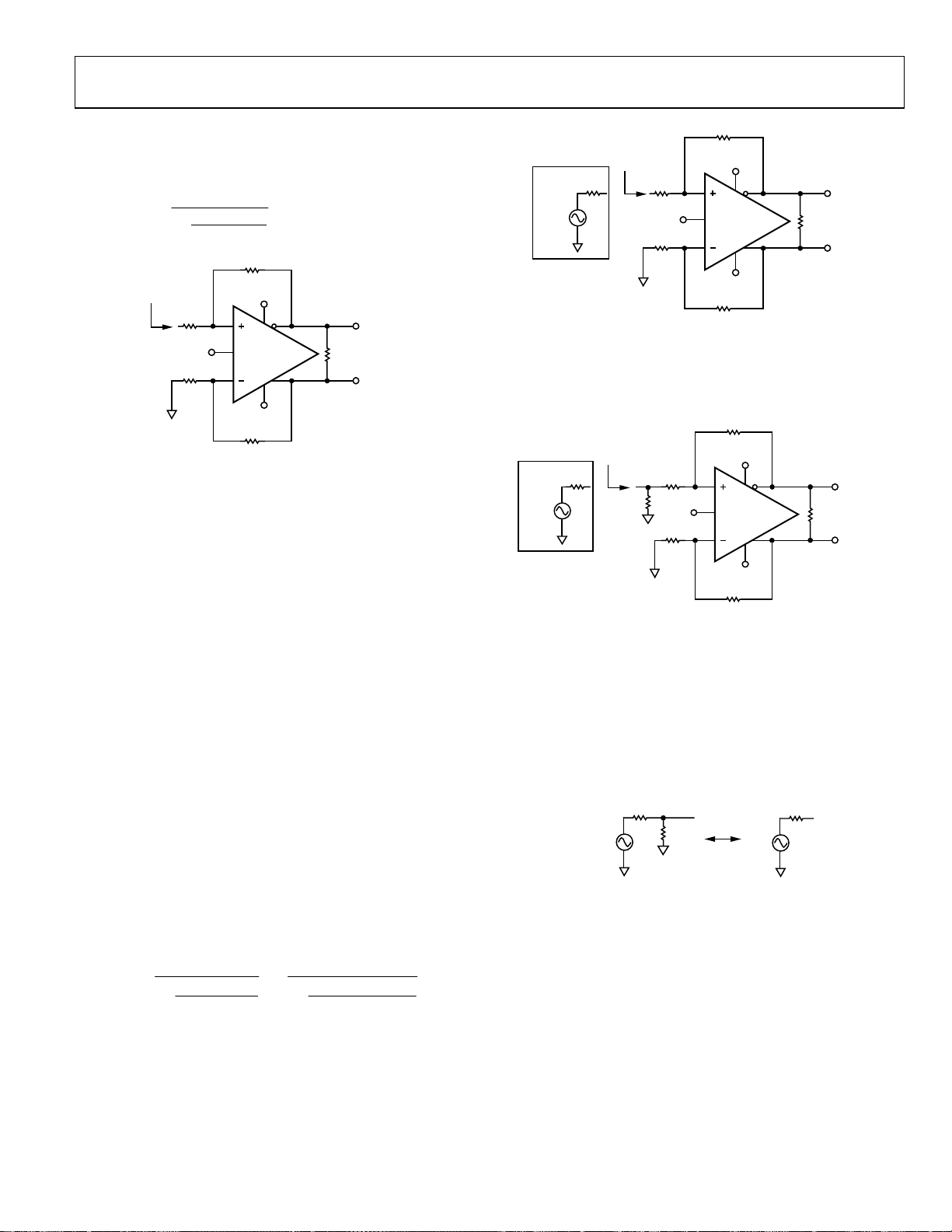
CALCULATING THE INPUT IMPEDANCE FOR AN APPLICATION CIRCUIT
The effective input impedance of a circuit depends on whether
the amplifier is being driven by a single-ended or differential
signal source. For balanced differential input signals, as shown
in Figure 48, the input impedance (R
and −DIN) is simply R
(+D
IN
R
G
+IN
V
OCM
–IN
R
G
input
OCM
Rev. A | Page 18 of 24
+D
IN
–D
IN
Figure 48. The ADA4927 Configured for Balanced (Differential) Inputs
to V
OCM
noise contribution,
OCM
) between the inputs
IN, dm
= RG + RG = 2 × RG.
IN, dm
R
F
+V
S
ADA4927
–V
S
R
F
is 0.67. If the
O, dm
V
OUT, dm
07574-048
Page 19
ADA4927-1/ADA4927-2
2
p
For an unbalanced, single-ended input signal (see Figure 49),
the input impedance is
F
+×
RR
F
R
F
+V
ADA4927
–V
R
F
⎞
⎟
⎟
⎟
⎟
⎠
S
RLV
OUT, dm
S
7574-049
⎛
⎜
⎜
=
R
SEIN
,
⎜
⎜
⎝
R
IN, SE
R
G
R
−
1
()
2
G
R
G
V
OCM
R
G
Figure 49. The ADA4927 with Unbalanced (Single-Ended) Input
The input impedance of the circuit is effectively higher than it
would be for a conventional op amp connected as an inverter
because a fraction of the differential output voltage appears at
the inputs as a common-mode signal, partially bootstrapping
the voltage across the input resistor R
. The common-mode
G
voltage at the amplifier input terminals can be easily determined
by noting that the voltage at the inverting input is equal to the
noninverting output voltage divided down by the voltage divider
formed by R
and RG in the lower loop. This voltage is present at
F
both input terminals due to negative voltage feedback and is in
phase with the input signal, thus reducing the effective voltage
across R
in the upper loop and partially bootstrapping RG.
G
Terminating a Single-Ended Input
This section deals with how to properly terminate a singleended input to the ADA4927 with a gain of 1, R
R
= 348 Ω. An example using an input source with a terminated
G
= 348 Ω, and
F
output voltage of 1 V p-p and a source resistance of 50 Ω illustrates
the four simple steps that must be followed. Note that, because
the terminated output voltage of the source is 1 V p-p, the open
circuit output voltage of the source is 2 V p-p. The source shown
in Figure 50 indicates this open-circuit voltage.
1.
The input impedance must be calculated using the following
formula:
⎛
⎜
⎜
=
R
IN
⎜
⎜
⎝
R
G
R
−
1
⎞
⎛
⎟
⎜
⎟
⎜
=
⎟
F
+×
⎜
−
1
⎟
⎜
)(2
RR
⎝
⎠
FG
348
348
+×
⎞
⎟
⎟
=
⎟
⎟
)348348(2
⎠
R
F
348Ω
+V
S
ADA4927
–V
S
R
F
348Ω
2V p-p
R
IN
464Ω
R
S
50Ω
V
S
R
348Ω
V
OCM
R
348Ω
G
G
Figure 50. Calculating Single-Ended Input Impedance R
2. To match the 50 Ω source resistance, the termination
resistor, R
closest standard 1% value for R
V
S
2V p-p
, is calculated using RT||464 Ω = 50 Ω. The
T
is 56.2 Ω.
T
R
F
348Ω
+V
S
ADA4927
–V
S
R
F
348Ω
R
50Ω
R
IN
50Ω
S
56.2Ω
R
G
348Ω
R
T
V
OCM
R
G
348Ω
Figure 51. Adding Termination Resistor R
3. It can be seen from Figure 51 that the effective RG in the
upper feedback loop is now greater than the R
lower loop due to the addition of the termination resistors.
To compensate for the imbalance of the gain resistors,
a correction resistor (R
lower loop. R
is equal to the Thevenin equivalent of the
TS
source resistance R
is equal to R
||RT.
S
R
S
50Ω
V
S
V p-
Figure 52. Calculating the Thevenin Equivalent
) is added in series with RG in the
TS
and the termination resistance RT and
S
R
T
56.2Ω
V
1.06V p-p
TH
Ω464
R
TH
26.5Ω
RLV
T
OUT, dm
IN
RLV
in the
G
7574-052
OUT, dm
07574-050
7574-051
Rev. A | Page 19 of 24
Page 20
ADA4927-1/ADA4927-2
RTS = RTH = RS||RT = 26.5 Ω. Note that VTH is greater than
1 V p-p, which was obtained with R
= 50 Ω. The modified
T
circuit with the Thevenin equivalent (closest 1% value used for
R
) of the terminated source and RTS in the lower feedback
TH
loop is shown in Figure 53.
R
F
348Ω
+V
S
R
R
TH
G
26.7Ω
R
26.7Ω
348Ω
V
OCM
R
G
348Ω
TS
ADA4927
–V
S
R
F
348Ω
V
R
OUT, dm
L
V
1.06V p-p
TH
Figure 53. Thevenin Equivalent and Matched Gain Resistors
Figure 53 presents a tractable circuit with matched
feedback loops that can be easily evaluated.
It is useful to point out two effects that occur with a
terminated input. The first is that the value of R
is increased
G
in both loops, lowering the overall closed-loop gain. The
second is that V
when R
= 50 Ω. These two effects have opposite impacts
T
is a little larger than 1 V p-p, as it is
TH
on the output voltage, and for large resistor values in the
feedback loops (~1 kΩ), the effects essentially cancel each
other out. For small R
and RG, or high gains, however, the
F
diminished closed-loop gain is not canceled completely by the
increased V
. This can be seen by evaluating Figure 53.
TH
The desired differential output in this example is 1 V p-p
because the terminated input signal is 1 V p-p and the
closed-loop gain = 1. The actual differential output voltage,
however, is equal to (1.06 V p-p)(348/374.7) = 0.984 V p-p.
To obtain the desired output voltage of 1 V p-p, a final gain
adjustment can be made by increasing R
without modifying
F
any of the input circuitry. This is discussed in Step 4.
The feedback resistor value is modified as a final gain
4.
adjustment to obtain the desired output voltage.
To make the output voltage V
= 1 V p-p, RF must be
OUT
calculated using the following formula:
=R
F
()
()
+
G
,
dmOUT
V
TH
()()
RRVDesired
TS
=
−
ppV
06.1
374.71
−
ppV
The closest standard 1% values to 353 Ω are 348 Ω and
357 Ω. Choosing 357 Ω for R
gives a differential output
F
voltage of 1.01 V p-p. The closed-loop bandwidth is
diminished by a factor of approximately 348/357 from
what it would be with R
proportional relationship between R
= 348 Ω due to the inversely
F
and closed-loop
F
gain that is characteristic of current feedback amplifiers.
The final circuit is shown in Figure 54.
07574-053
35
=
Rev. A | Page 20 of 24
R
F
357Ω
+V
S
ADA4927
–V
S
R
F
357Ω
R
L
V
OUT, dm
1.01V p-p
2V p-p
1V p-p
R
S
50Ω
V
S
56.2Ω
R
R
26.7Ω
R
G
348Ω
T
V
OCM
R
G
348Ω
TS
Figure 54. Terminated Single-Ended-to-Differential System with G = 1
INPUT COMMON-MODE VOLTAGE RANGE
The ADA4927 input common-mode range is centered between the
two supply rails, in contrast to other ADC drivers with level-shifted
input ranges, such as the ADA4937. The centered input common-
mode range is best suited to ac-coupled, differential-to-differential,
and dual supply applications.
For operation with ±5 V supplies, the input common-mode
range at the summing nodes of the amplifier is specified as
−3.5 V to +3.5 V and is specified as +1.3 V to +3.7 V with a
single +5 V supply. To avoid nonlinearities, the voltage swing
at the +IN and −IN terminals must be confined to these ranges.
INPUT AND OUTPUT CAPACITIVE AC COUPLING
Input ac coupling capacitors can be inserted between the source
. This ac coupling blocks the flow of the dc common-
and R
G
mode feedback current and causes the ADA4927 dc input
common-mode voltage to equal the dc output common-mode
voltage. These ac coupling capacitors must be placed in both
loops to keep the feedback factors matched.
Output ac coupling capacitors can be placed in series between
each output and its respective load. See Figure 58 for an example
that uses input and output capacitive ac coupling.
SETTING THE OUTPUT COMMON-MODE VOLTAGE
The V
divider comprising two 10 kΩ resistors at a voltage approximately
equal to the midsupply point, [(+V
internal divider, the V
on the externally applied voltage and its associated source resistance.
Relying on the internal bias results in an output common-mode
voltage that is within about 100 mV of the expected value.
In cases where accurate control of the output common-mode level
is required, it is recommended that an external source or resistor
divider be used with source resistance less than 100 Ω. The output
common-mode offset listed in the Specifications section presumes
that the V
It is also possible to connect the V
level (CML) output of an ADC; however, care must be taken to
ensure that the output has sufficient drive capability. The input
impedance of the V
ADA4927 devices share one ADC reference output, a buffer may
be necessary to drive the parallel inputs.
pin of the ADA4927 is internally biased with a voltage
OCM
) + (−VS)]/2. Because of this
S
pin sources and sinks current, depending
OCM
input is driven by a low impedance voltage source.
OCM
input to a common-mode
OCM
pin is approximately 10 kΩ. If multiple
OCM
07574-054
Page 21

ADA4927-1/ADA4927-2
POWER-DOWN
The power-down feature can be used to reduce power
consumption when a particular device is not in use and does
not place the output in a high-Z state when asserted. The
ADA4927 is generally enabled by pulling the power-down pin
to the positive supply. See the Specifications tables for the
specific voltages required to assert and deassert the powerdown feature.
Power-Down in Cold Applications
The power-down feature should not be used in applications in
which the ambient temperature falls below 0°C. Contact sales
for information regarding applications that require the powerdown feature to be used at ambient temperatures below 0°C.
Rev. A | Page 21 of 24
Page 22
ADA4927-1/ADA4927-2
LAYOUT, GROUNDING, AND BYPASSING
As a high speed device, the ADA4927 is sensitive to the PCB
environment in which it operates. Realizing its superior performance
requires attention to the details of high speed PCB design. This
section shows a detailed example of how the ADA4927-1 was
addressed.
The first requirement is a solid ground plane that covers as
much of the board area around the ADA4927-1 as possible.
However, clear the area near the feedback resistors (RF), gain
resistors (RG), and the input summing nodes (Pin 2 and Pin 3) of
all ground and power planes (see Figure 55). Clearing the ground
and power planes minimizes any stray capacitance at these nodes
and prevents peaking of the response of the amplifier at high
frequencies. Whereas ideal current feedback amplifiers are
insensitive to summing node capacitance, real-world amplifiers
can exhibit peaking due to excessive summing node capacitance.
The thermal resistance, θ
, is specified for the device, including
JA
the exposed pad, soldered to a high thermal conductivity 4-layer
circuit board, as described in EIA/JESD 51-7.
Bypassed the power supply pins as close to the device as possible
and directly to a nearby ground plane. Use high frequency ceramic
chip capacitors. It is recommended that two parallel bypass
capacitors (1000 pF and 0.1 µF) be used for each supply. The
1000 pF capacitor should be placed closer to the device. Further
away, provide low frequency bulk bypassing, using 10 µF
tantalum capacitors from each supply to ground.
Make signal routing short and direct to avoid parasitic effects.
Wherever complementary signals exist, provide a symmetrical
layout to maximize balanced performance. When routing
differential signals over a long distance, place PCB traces close
together, and twist any differential wiring such that the loop
area is minimized. Doing this reduces radiated energy and
makes the circuit less susceptible to interference.
1.30
0.80
7574-055
Figure 55. Ground and Power Plane Voiding in Vicinity of RF AND RG
TOP METAL
GROUND PLANE
1.30
0.80
07574-056
Figure 56. Recommended PCB Thermal Attach Pad Dimensions (Millimeters)
1.30
0.30
PLATED
VIA HOLE
POWE R PLANE
BOTTOM M ETAL
Figure 57. Cross-Section of 4-Layer PCB Showing Thermal Via Connection to Buried Ground Plane (Dimensions in Millimeters)
4-0570757
Rev. A | Page 22 of 24
Page 23
ADA4927-1/ADA4927-2
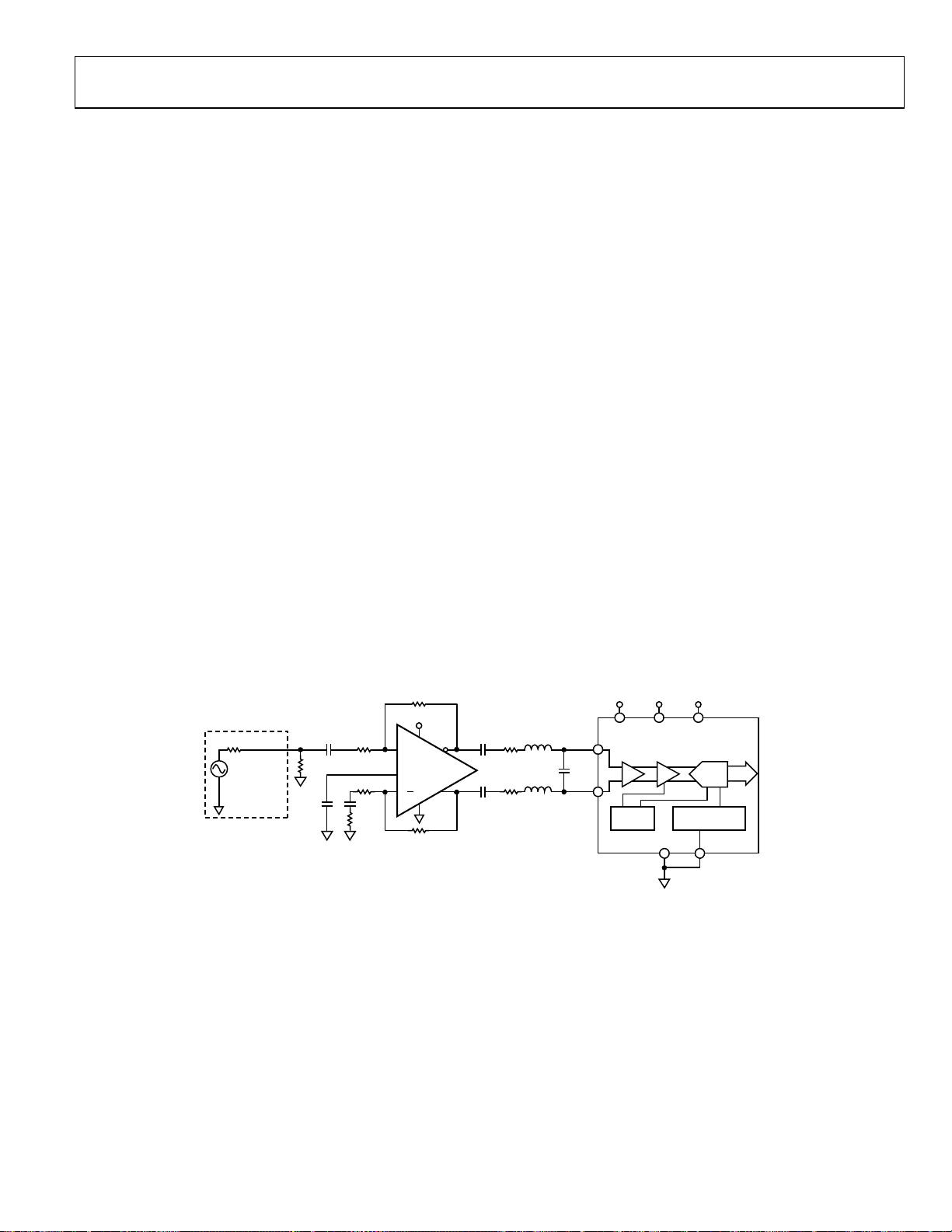
HIGH PERFORMANCE ADC DRIVING
The ADA4927 is ideally suited for high gain, broadband accoupled and differential-to-differential applications on a single
supply, though other applications are possible. Compared with
voltage feedback amplifiers, the current feedback architecture
provides superior distortion and bandwidth performance at
high gains. This is because the ideal current feedback amplifier
loop gain depends only on the feedback value and open-loop
transimpedance, T(s).
The circuit in Figure 58 shows a front-end connection for an
ADA4927 driving an AD9445, 14-bit, 105 MSPS ADC, with ac
coupling on the ADA4927 input and output. (The AD9445
achieves its optimum performance when driven differentially.)
The ADA4927 eliminates the need for a transformer to drive
the ADC and performs a single-ended-to-differential conversion
and buffering of the driving signal.
The ADA4927 is configured with a single 5 V supply and gain
of 10 for a single-ended input to differential output. The 158 Ω
termination resistor, in parallel with the single-ended input
impedance of approximately 73.2 Ω, provides a 50 Ω termination
for the source. The additional 38.3 Ω at the inverting input closely
matches the parallel impedance of the 50 Ω source and the
termination resistor driving the noninverting input. Because of the
high gain, a few iterations of the termination technique described
in the Terminating a Single-Ended Input section are required.
Two objectives of the design are to make R
close to 500 Ω and
F
obtain resistor values that are close to standard 1% values.
511Ω
5V
158Ω
39.2Ω
V
39.2Ω
0.1µF0.1µF
38.3Ω
OCM
+
ADA4927
511Ω
50Ω
SIGNAL
GENERATOR
In this example, the signal generator has a 1 V p-p symmetric,
ground-referenced bipolar output when terminated in 50 Ω.
The V
pin of the ADA4927 is bypassed for noise reduction
OCM
and left floating such that the internal divider sets the output
common-mode voltage nominally at midsupply. Because the
inputs are ac-coupled, no dc common-mode current flows in
the feedback loops, and a nominal dc level of midsupply is
present at the amplifier input terminals. Besides placing the
amplifier inputs at their optimum levels, the ac coupling technique
lightens the load on the amplifier and dissipates less power than
applications with dc-coupled inputs.
The output of the amplifier is ac-coupled to the ADC through a
second-order, low-pass filter with a cutoff frequency of 100 MHz.
This reduces the noise bandwidth of the amplifier and isolates
the driver outputs from the ADC inputs.
The AD9445 is configured for a 2 V p-p full-scale input by
connecting the SENSE pin to AGND, as shown in Figure 58.
3.3V (A)
0.1µF0.1µF
0.1µF
24.3Ω
24.3Ω
30nH
30nH
VIN–
47pF
VIN+
5V (A)
AVDD2
BUFFER T/H
CLOCK/
TIMING
AVDD1
3.3V (D)
DRVDD
ADC
REF
AD9445
14
SENSEAGND
07574-058
Figure 58. ADA4927 Driving an AD9445 ADC with AC-Coupled Input and Output
Rev. A | Page 23 of 24
Page 24

ADA4927-1/ADA4927-2
OUTLINE DIMENSIONS
0.50
0.40
PIN 1
INDICATOR
1.00
0.85
0.80
SEATING
PLANE
12° MAX
3.00
BSC SQ
TOP
VIEW
0.30
0.23
0.18
*
COMPLIANT
EXCEPT FOR EXPOSED PAD DIMENSI ON.
2.75
BSC SQ
0.80 MAX
0.65 TYP
0.05 MAX
0.02 NOM
0.20 REF
TO
JEDEC STANDARDS MO-220-VEED-2
0.45
0.50
BSC
1.50 REF
0.60 MAX
13
12
9
8
FOR PROPER CONNECTION O F
THE EXPOSED PAD, REFER TO
THE PIN CONF IGURATIO N AND
FUNCTION DESCRIPTIONS
SECTION OF THIS DATA SHEET.
Figure 59. 16-Lead Lead Frame Chip Scale Package [LFCSP_VQ]
3 mm × 3 mm Body, Very Thin Quad (CP-16-2)
Dimensions shown in millimeters
(BOTTOM VIEW)
EXPOSED
PAD
0.30
16
1
4
5
PIN 1
INDICATOR
*
1.45
1.30 SQ
1.15
0.25 MIN
072208-A
0.60 MAX
PIN 1
INDICATOR
1
24
19
18
EXPOSED
PAD
(BOTTOM VIEW)
13
7
12
FOR PROPER CONNECTION OF
THE EXPOSED PAD, REFER TO
THE PIN CONF IGURATIO N AND
FUNCTION DESCRI PTIONS
SECTION O F THIS DATA S HEET.
2.25
2.10 SQ
1.95
6
0.25 MIN
072208-A
PIN 1
INDICATOR
1.00
0.85
0.80
12° MAX
SEATING
PLANE
4.00
BSC SQ
TOP
VIEW
0.80 MAX
0.65 TYP
COMPLIANT TO JEDEC STANDARDS MO-220-VGGD-2
0.30
0.23
0.18
3.75
BSC SQ
0.20 REF
0.60 MAX
0.05 MAX
0.02 NOM
COPLANARITY
0.08
0.50
BSC
0.50
0.40
0.30
2.50 REF
Figure 60. 24-Lead Lead Frame Chip Scale Package [LFCSP_VQ]
4 mm × 4 mm Body, Very Thin Quad (CP-24-1)
Dimensions shown in millimeters
ORDERING GUIDE
Model Temperature Range Package Description Package Option Ordering Quantity Branding
ADA4927-1YCPZ-R2
ADA4927-1YCPZ-RL
ADA4927-1YCPZ-R7
ADA4927-2YCPZ-R2
ADA4927-2YCPZ-RL
ADA4927-2YCPZ-R7
1
Z = RoHS Compliant Part.
1
1
1
1
1
1
−40°C to +105°C 16-Lead LFCSP_VQ CP-16-2 250 H1N
−40°C to +105°C 16-Lead LFCSP_VQ CP-16-2 5,000 H1N
−40°C to +105°C 16-Lead LFCSP_VQ CP-16-2 1,500 H1N
−40°C to +105°C 24-Lead LFCSP_VQ CP-24-1 250
−40°C to +105°C 24-Lead LFCSP_VQ CP-24-1 5,000
−40°C to +105°C 24-Lead LFCSP_VQ CP-24-1 1,500
©2008-2009 Analog Devices, Inc. All rights reserved. Trademarks and
registered trademarks are the property of their respective owners.
D07574-0-8/09(A)
Rev. A | Page 24 of 24
 Loading...