

High Voltage, Differential
O
www.BDTIC.com/ADI
FEATURES
Single-ended-to-differential conversion
Low distortion (V
−99 dBc HD at 100 kHz
Low differential output referred noise: 12 nV/√Hz
High input impedance: 11 MΩ
Fixed gain of 2
No external gain components required
Low output-referred offset voltage: 1.1 mV max
Low input bias current: 3.5 μA max
Wide supply range
5 V to 26 V
Can produce differential output signals in excess of 40 V p-p
High speed
38 MHz, −3 dB bandwidth @ 0.2 V p-p differential output
Fast settling time
200 ns to 0.01% for 12 V step on ±5 V supplies
Disable feature
Available in space-saving, thermally enhanced packages
3 mm × 3 mm LFCSP
8-lead SOIC_EP
Low supply current: I
APPLICATIONS
High voltage data acquisition systems
Industrial instrumentation
Spectrum analysis
ATE
Medical instruments
GENERAL DESCRIPTION
= 40 V p-p)
O, dm
= 10 mA on ±12 V supplies
S
–84
–87
–90
–93
–96
–99
–102
–105
–108
DISTORTION (dBc)
–111
–114
–117
–120
18-Bit ADC Driver
ADA4922-1
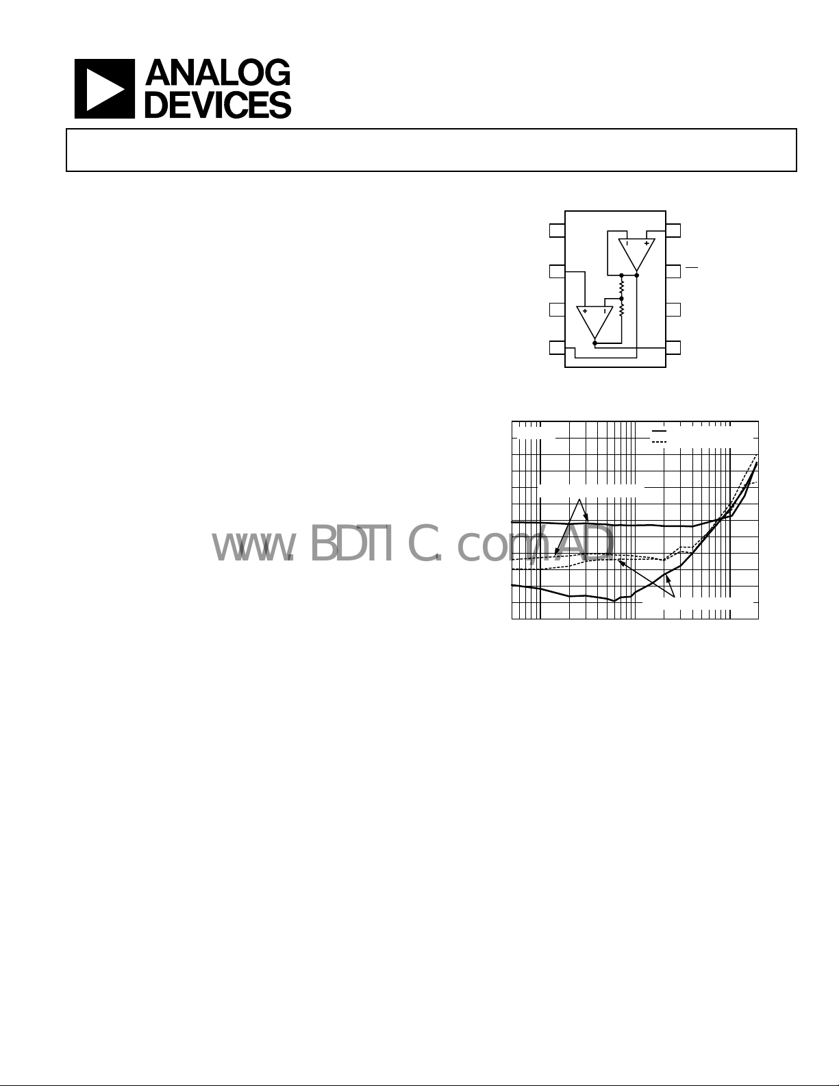
FUNCTIONAL BLOCK DIAGRAM
ADA4922-1
1
NC
2
REF
V
3
S+
4
UT+
NC = NO CONNECT
Figure 1.
RL= 2kΩ
VS = ±5V, V
1 10 100
Figure 2. Harmonic Distortion for Various Power Supplies
= 12V p-p
O, dm
FREQUENCY (kHz)
8
IN
7
DIS
6
V
S–
5
OUT–
SECOND HARMONIC
THIRD HARMONIC
VS = ±12V, V
O, dm
05681-001
= 40V p-p
05681-012
The ADA4922-1 is a differential driver for 16-bit to 18-bit
ADCs that have differential input ranges up to ±20 V.
Configured as an easy-to-use, single-ended-to-differential
amplifier, the ADA4922-1 requires no external components to
drive ADCs. The ADA4922-1 provides essential benefits such as
low distortion and high SNR that are required for driving ADCs
with resolutions up to 18 bits.
With a wide supply voltage range (5 V to 26 V), high input
pedance, and fixed differential gain of 2, the ADA4922-1 is
im
designed to drive ADCs found to in a variety of applications,
including industrial instrumentation.
Rev. 0
Information furnished by Analog Devices is believed to be accurate and reliable. However, no
responsibility is assumed by Anal og Devices for its use, nor for any infringements of patents or ot her
rights of third parties that may result from its use. Specifications subject to change without notice. No
license is granted by implication or otherwise under any patent or patent rights of Analog Devices.
Trademarks and registered trademarks are the property of their respective owners.
The ADA4922-1 is manufactured on ADI’s proprietary secondg
eneration XFCB process that enables the amplifier to achieve
excellent noise and distortion performance on high supply
voltages.
The ADA4922-1 is available in an 8-lead 3 mm × 3 mm LFCSP
as w
ell as an 8-lead SOIC package. Both packages are equipped
with an exposed paddle for more efficient heat transfer. The
ADA4922-1 is rated to work over the extended industrial
temperature range, −40°C to +85°C.
One Technology Way, P.O. Box 9106, Norwood, MA 02062-9106, U.S.A.
Tel: 781.329.4700 www.analog.com
Fax: 781.461.3113 © 2005 Analog Devices, Inc. All rights reserved.

ADA4922-1
www.BDTIC.com/ADI
TABLE OF CONTENTS
Features .............................................................................................. 1
Theory of Operation ...................................................................... 14
Applications....................................................................................... 1
Functional Block Diagram .............................................................. 1
General Description......................................................................... 1
Revision History ............................................................................... 2
Specifications..................................................................................... 3
Absolute Maximum Ratings............................................................ 5
Thermal Resistance ...................................................................... 5
ESD Caution.................................................................................. 5
Pin Configuration and Function Descriptions............................. 6
Typical Performance Characteristics............................................. 7
REVISION HISTORY
10/05—Revision 0: Initial Version
Applications..................................................................................... 16
ADA4922-1 Differential Output Noise Model .......................... 16
Using the REF Pin ...................................................................... 16
Internal Feedback Network Power Dissipation...................... 17
Disable Feature........................................................................... 17
Driving a Differential Input ADC............................................ 17
Printed Circuit Board Layout Considerations ....................... 18
Outline Dimensions .......................................................................19
Ordering Guide .......................................................................... 20
Rev. 0 | Page 2 of 20
ADA4922-1
www.BDTIC.com/ADI
SPECIFICATIONS
VS = ±12 V, TA = 25°C, RL = 1 kΩ,
Table 1.
Parameter Conditions Min Typ Max Unit
DYNAMIC PERFORMANCE
–3 dB Bandwidth G = +2, VO = 0.2 V p-p, differential 34 38 MHz
G = +2, VO = 40 V p-p, differential 6.5 7.2 MHz
Overdrive Recovery Time VS+ + 0.5 V to VS− − 0.5 V; +Recovery/−Recovery 180/330 ns
Slew Rate V
V
Settling Time to 0.01% V
NOISE/DISTORTION PERFORMANCE
Harmonic Distortion fC = 5 kHz, VO = 40 V p-p, RL = 2 kΩ, HD2/HD3 −116/−109 dBc
f
Differential Output Voltage Noise f = 100 kHz 12 nV/√Hz
Input Current Noise f = 100 kHz 1.4 pA/√Hz
DC PERFORMANCE
Differential Output Offset Voltage 0.35 1.1 mV
Differential Output Offset Voltage Drift 14 μV/°C
Input Bias Current 1.8 3.5 μA
Gain 2 V/V
Gain Error −0.05 %
Gain Error Drift 0.0002 %/°C
INPUT CHARACTERISTICS
Input Resistance 11 MΩ
Input Capacitance 1 pF
Input Voltage Range
OUTPUT CHARACTERISTICS
Output Voltage Swing Each single-ended output, RL = 1 kΩ
DC Output Current 40 mA
Capacitive Load Drive 30% overshoot 20 pF
POWER SUPPLY
Operating Range 5 26 V
Quiescent Current 9.4 10.1 mA
Quiescent Current (Disabled) 1.5 2.0 mA
Power Supply Rejection Ratio (PSRR)
−PSRR −89 −80 dB
+PSRR −91 −83 dB
DISABLE
DIS Input Voltage Threshold
Enabled ≥ −9 V
Turn-Off Time 160 μs
Turn-On Time 78 ns
DIS Bias Current
Enabled
Disabled
= HIGH, CL = 3 pF, unless otherwise noted.
DIS
= 2 V step 260 V/μs
O, dm
= 40 V step 730 V/μs
O, dm
= 40 V step 580 ns
O, dm
= 100 kHz, VO = 40 V p-p, RL = 2 kΩ, HD2/HD3 −99/−100 dBc
C
Disabled ≤ −11 V
= −9 V
DIS
= −11 V
DIS
±10.7
±10.65 ±10.7
114 μA
−125 μA
V
V
Rev. 0 | Page 3 of 20

ADA4922-1
www.BDTIC.com/ADI
VS = ±5 V, TA = 25°C, RL = 1 kΩ,
Table 2.
Parameter Conditions Min Typ Max Unit
DYNAMIC PERFORMANCE
–3 dB Bandwidth G = +2, VO = 0.2 V p-p, differential 36 40.5 MHz
G = +2, VO = 12 V p-p, differential 6.5 13.5 MHz
Overdrive Recovery Time +Recovery/−Recovery 200/670 ns
Slew Rate V
V
Settling Time to 0.01% V
NOISE/DISTORTION PERFORMANCE
Harmonic Distortion fC = 5 kHz, VO = 12 V p-p, RL = 2 kΩ, HD2/HD3 −102/−108 dBc
f
Differential Output Voltage Noise f = 100 kHz 12 nV/√Hz
Input Current Noise f = 100 kHz 1.4 pA/√Hz
DC PERFORMANCE
Differential Output Offset Voltage 0.4 1.2 mV
Differential Output Offset Voltage Drift 12 μV/°C
Input Bias Current 2.0 3.5 μA
Gain 2 V/V
Gain Error −0.05 %
Gain Error Drift 0.0002 %/°C
INPUT CHARACTERISTICS
Input Resistance 11 MΩ
Input Capacitance 1 pF
Input Voltage Range
OUTPUT CHARACTERISTICS
Output Voltage Swing Each single-ended output, RL = 1 kΩ
DC Output Current 40 mA
Capacitive Load Drive 30% overshoot 20 pF
POWER SUPPLY
Operating Range 5 26 V
Quiescent Current 7.0 7.6 mA
Quiescent Current (Disabled) 0.7 1.6 mA
Power Supply Rejection Ratio (PSRR)
−PSRR −93 −82 dB
+PSRR −91 −83 dB
DISABLE
DIS Input Voltage
Enabled ≥ −2 V
Turn-Off Time 160 μs
Turn-On Time 78 ns
DIS Bias Current
Enabled
Disabled
= HIGH, CL = 3 pF, unless otherwise noted.
DIS
= 2 V step 220 V/μs
O, dm
= 12 V step 350 V/μs
O, dm
= 12 V step 200 ns
O, dm
= 100 kHz, VO = 12 V p-p, RL = 2 kΩ, HD2/HD3 −101/−98 dBc
C
Disabled ≤ −4 V
= −2 V
DIS
= −4 V
DIS
±3.6
±3.55 ±3.6
41 μA
49 μA
V
V
Rev. 0 | Page 4 of 20
ADA4922-1
www.BDTIC.com/ADI
ABSOLUTE MAXIMUM RATINGS
Table 3.
Parameter Rating
Supply Voltage 26 V
Power Dissipation See Figure 3
Storage Temperature Range –65°C to +125°C
Operating Temperature Range –40°C to +85°C
Lead Temperature Range (Soldering 10 sec) 300°C
Junction Temperature 150°C
Stresses above those listed under Absolute Maximum Ratings
may cause permanent damage to the device. This is a stress
rating only; functional operation of the device at these or any
other conditions above those indicated in the operational
section of this specification is not implied. Exposure to absolute
maximum rating conditions for extended periods may affect
device reliability.
THERMAL RESISTANCE
θJA is specified for the worst-case conditions, that is, θJA is
specified for a device soldered in the circuit board with its
exposed paddle soldered to a pad on the PCB surface that is
thermally connected to a copper plane, with zero airflow.
Table 4. Thermal Resistance
Package Type θ
8-Lead SOIC with EP on 4-layer board 79 25
8-Lead LFCSP with EP on 4-layer board 81 17
Maximum Power Dissipation
The maximum safe power dissipation in the ADA4922-1
package is limited by the associated rise in junction temperature
(T
) on the die. At approximately 150°C, which is the glass
J
transition temperature, the plastic changes its properties. Even
temporarily exceeding this temperature limit can change the
stresses that the package exerts on the die, permanently shifting
the parametric performance of the ADA4922-1. Exceeding a
junction temperature of 150°C for an extended period can
result in changes in the silicon devices potentially causing
failure.
θ
JA
Unit
JC
°C/W
°C/W
The power dissipated in the package (P
) is the sum of the
D
quiescent power dissipation and the power dissipated in the
package due to the load drive for all outputs. The quiescent
power is the voltage between the supply pins (V
quiescent current (I
). The power dissipated due to the load
S
) times the
S
drive depends upon the particular application. For each output,
the power due to load drive is calculated by multiplying the load
current by the associated voltage drop across the device. The
power dissipated due to all of the loads is equal to the sum of
the power dissipation due to each individual load. RMS voltages
and currents must be used in these calculations.
Airflow increases heat dissipation, effectively reducing θ
JA
. In
addition, more metal directly in contact with the package leads
from metal traces, through holes, ground, and power planes
reduces the θ
. The exposed paddle on the underside of the
JA
package must be soldered to a pad on the PCB surface that is
thermally connected to a copper plane to achieve the specified θ
.
JA
Figure 3 shows the maximum safe power dissipation in the
ckages vs. the ambient temperature for the 8-lead SOIC
pa
(79°C/W) and for the 8-lead LFCSP (81°C/W) on a JEDEC
standard 4-layer board, each with its underside paddle soldered
to a pad that is thermally connected to a PCB plane. θ
values
JA
are approximations.
3.0
2.5
2.0
1.5
1.0
0.5
MAXIMUM POWER DISSIPATION (W)
0
–40 80
Figure 3. Maximum Power Dissipation vs. Temperature for a 4-Layer Board
SOIC
LFCSP
–20 0 20 40 60
AMBIENT TEMPERATURE (°C)
05681-041
ESD CAUTION
ESD (electrostatic discharge) sensitive device. Electrostatic charges as high as 4000 V readily accumulate on
the human body and test equipment and can discharge without detection. Although this product features
proprietary ESD protection circuitry, permanent damage may occur on devices subjected to high energy
electrostatic discharges. Therefore, proper ESD precautions are recommended to avoid performance
degradation or loss of functionality.
Rev. 0 | Page 5 of 20
ADA4922-1
O
www.BDTIC.com/ADI
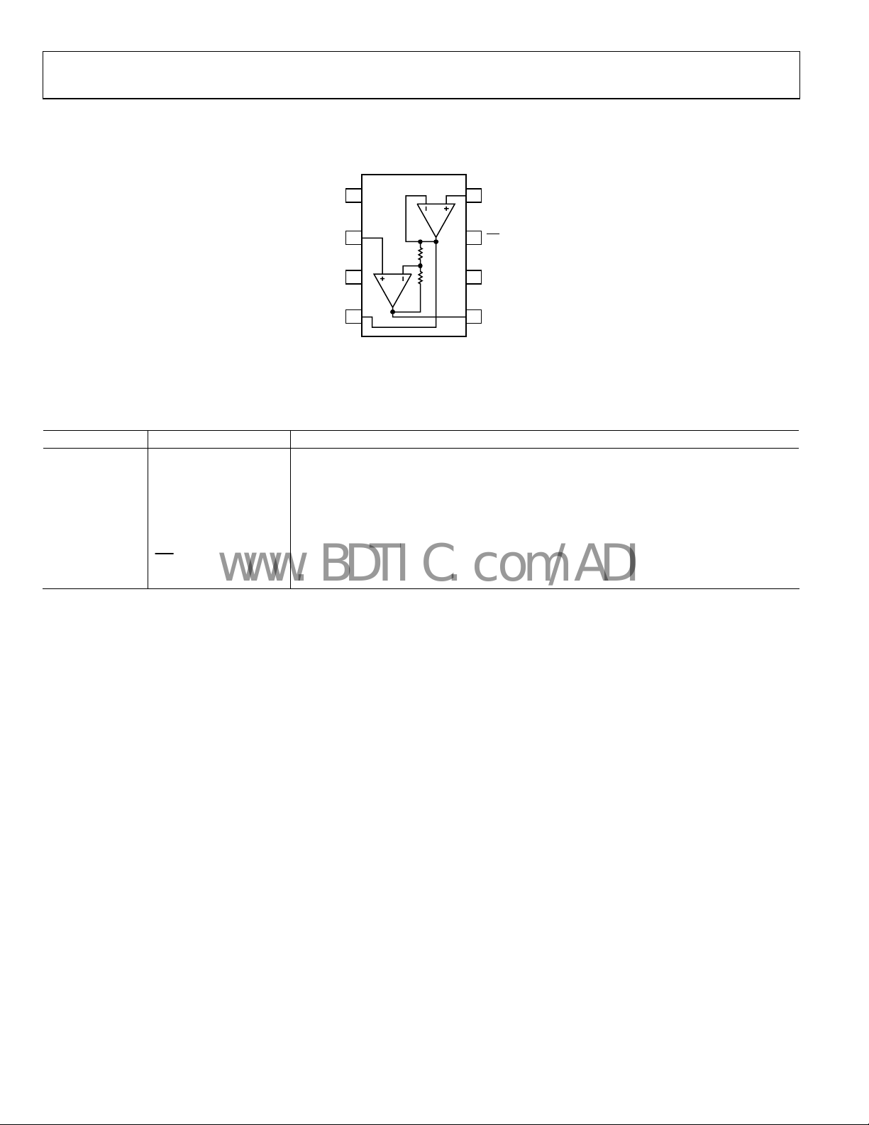
PIN CONFIGURATION AND FUNCTION DESCRIPTIONS
ADA4922-1
1
NC
2
REF
3
V
S+
4
UT+
NC = NO CONNECT
Figure 4. Pin Configuration
8
IN
7
DIS
6
V
S–
5
OUT–
05681-001
Table 5. Pin Function Descriptions
Pin No. Mnemonic Description
1 NC No Internal Connection
2 REF Reference Voltage for Single-Ended Input Signal
3 V
S+
Positive Power Supply
4 OUT+ Noninverting Side of Differential Output
5 OUT− Inverting Side of Differential Output
6 V
7
S−
DIS
Negative Power Supply
Disable
8 IN Single-Ended Signal Input
Rev. 0 | Page 6 of 20

ADA4922-1
www.BDTIC.com/ADI
TYPICAL PERFORMANCE CHARACTERISTICS
Unless otherwise noted, VS = ±12 V, R
3
0
–3
–6
–9
–12
–15
–18
–21
–24
NORMALIZED CLOSED-LOOP GAIN (dB)
–27
–30
1
Figure 5. Small Signal Frequency Response for Various Power Supplies
3
0
–3
–6
–9
–12
–15
–18
VS =±12V @ +85°C
–21
VS =±5V @ +85°C
VS =±12V @ +25°C
–24
–27
–30
1
VS =±5V @ +25°C
VS =±12V @ –40°C
VS =±5V @ –40°C
NORMALIZED CLOSED-LOOP GAIN (dB)
Figure 6. Small Signal Fr
Various Temperatures and Supplies
3
0
–3
–6
–9
–12
–15
–18
–21
VS =±12V R
–24
–27
–30
1
VS =±5V R
VS =±12V R
VS =±5V R
NORMALIZED CLOSED-LOOP GAIN (dB)
Figure 7. Small Signal Fr
Various Resistive Loads and Supplies
10 100
FREQUENCY (MHz)
10 100
FREQUENCY (MHz)
equency Response for
= 1k
Ω
L, dm
= 1k
Ω
L, dm
= 500
L, dm
L, dm
Ω
= 500
Ω
10 100
FREQUENCY (MHz)
equency Response for
= 1 kΩ, REF = 0 V,
L, dm
V
= 0.2V p-p
O, dm
VS =±5V
VS =±12V
V
= 0.2V p-p
O, dm
VO, dm = 0.2V p-p
1000
1000
1000
= HIGH, TA = 25°C.
DIS
05681-013
05681-014
05681-015
3
0
–3
–6
–9
–12
–15
–18
–21
–24
NORMALIZED CLOSED-LOOP GAIN (dB)
–27
–30
VS =±5V, V
VS =±12V, V
1
= 40V p-p
O, dm
10 100
FREQUENCY (MHz)
O, dm
= 12V p-p
Figure 8. Large Signal Frequency Response for Various Power Supplies
3
0
–3
–6
–9
V
= 12V p-p (VS =±5V)
O, dm
–12
V
= 40V p-p (VS =±12V)
O, dm
–15
–18
(ALL VOLTAGES ARE V
–21
–24
NORMALIZED CLOSED-LOOP GAIN (dB)
–27
–30
1
40V p-p +85°C
40V p-p +25°C
40V p-p –40°C
12V p-p +85°C
12V p-p +25°C
12V p-p –40°C
)
O, dm
10
FREQUENCY (MHz)
100
Figure 9. Large Signal Frequency Response at
Vari
ous Temperatures and Supplies
3
0
–3
–6
–9
V
= 12V p-p (VS =±5V)
O, dm
–12
V
= 40V p-p (VS =±12V)
O, dm
–15
–18
–21
–24
NORMALIZED CLOSED-LOOP GAIN (dB)
–27
–30
1
VS =±12V, R
VS =±5V, R
VS =±12V, R
VS =±5V, R
= 1k
Ω
L, dm
= 1k
Ω
L, dm
= 500
L, dm
L, dm
Ω
= 500
Ω
FREQUENCY (MHz)
10
100
Figure 10. Large Signal Frequency Response for
Va
rious Resistive Loads and Supplies
05681-016
05681-017
05681-018
Rev. 0 | Page 7 of 20

ADA4922-1
www.BDTIC.com/ADI
3
0
–3
–6
–9
–12
–15
–18
–21
–24
NORMALIZED CLOSED-LOOP GAIN (dB)
–27
–30
1
VS =±5V, C
VS =±5V, C
VS =±12V, C
VS =±12V, C
= 10pF
L, dm
= 20pF
L, dm
= 0pF
L, dm
= 20pF
L, dm
10 100
FREQUENCY (MHz)
VO, dm = 0.2V p-p
1000
05681-019
Figure 11. Small Signal Frequency Response for Various Capacitive Loads
3
0
–3
2V p-p
0.2V p-p
1000
= ±5 V
S
05681-020
–6
–9
–12
–15
–18
–21
NORMALIZED GAIN (dB)
–24
–27
–30
–33
1
16V p-p
12V p-p
10V p-p
10 100
FREQUENCY (MHz)
Figure 12. Frequency Response for Various Output Amplitudes, V
–50
VIN = 0.1V p-p
DIS = LOW
–60
–70
–80
–90
ISOLATION (dB)
–100
–110
–120
VS =±12V
V
±
5V
S
1 10 100
FREQUENCY (MHz)
1000
05681-011
Figure 13. Isolation vs. Frequency—Disabled
Figure 16. REF Small Signal Frequency
3
0
–3
–6
–9
–12
–15
–18
–21
–24
NORMALIZED CLOSED-LOOP GAIN (dB)
–27
–30
VS =±5V, VIN = 12V p-p, C
VS =±12V, VIN = 40V p-p, C
VS =±5V, VIN = 12V p-p, C
VS =±12V, VIN = 40V p-p, C
1
FREQUENCY (MHz)
10
L, dm
L, dm
L, dm
L, dm
= 0pF
= 0pF
= 20pF
= 20pF
100
05681-050
Figure 14. Large Signal Frequency Response for Various Capacitive Loads
3
0
–3
–6
2V p-p
0.2V p-p
1000
= ±12 V
S
05681-023
–9
–12
–15
–18
–21
NORMALIZED GAIN (dB)
–24
–27
–30
–33
1
10V p-p
20V p-p
40V p-p
10 100
FREQUENCY (MHz)
Figure 15. Frequency Response for Various Output Amplitudes, V
3
0
–3
–6
–9
–12
–15
–18
–21
–24
NORMALIZED CLOSED-LOOP GAIN (dB)
–27
–30
VS =±12V
1
10 100
FREQUENCY (MHz)
V
REF
VS =±5V
= 0.1V p-p
1000
05681-024
Response for Various Power Supplies
Rev. 0 | Page 8 of 20

ADA4922-1
www.BDTIC.com/ADI
–84
RL= 2k
–87
–90
–93
–96
–99
–102
–105
–108
DISTORTION (dBc)
–111
–114
–117
–120
VS =±5V, V
1 10 100
Ω
= 12V p-p
O, dm
FREQUENCY (kHz)
SECOND HARMONIC
THIRD HARMONIC
VS =±12V, V
O, dm
Figure 17. Harmonic Distortion for Various Power Supplies
–60
–70
RL= 2k
Ω
SECOND HARMONIC
THIRD HARMONIC
= 40V p-p
05681-012
–84
VS =±12V
–87
V
= 40V p-p
O, dm
–90
–93
–96
–99
RL= 600
–102
–105
–108
DISTORTION (dBc)
–111
–114
–117
–120
RL= 2k
1 10010
Ω
Ω
RL= 1k
FREQUENCY (kHz)
Figure 20. Harmonic Distortion for Various Loads
100
SECOND HARMONIC
THIRD HARMONIC
Ω
05681-022
–80
–90
VS =±5V
–100
–110
DISTORTION (dBc)
–120
–130
–140
72221712 42373227
OUTPUT AMPLITUDE (V p-p)
VS =±12V
Figure 18. Harmonic Distortion vs. Output Amplitude and
Supply Voltage (f =10 k
0
–10
–20
–30
–40
–50
PSRR (dB)
–60
–70
–80
–90
–100
0.001 0.01 10010.1 10
+PSRR
FREQUENCY (MHz)
Hz)
–PSRR
Figure 19. PSRR vs. Frequency
47
05681-021
05681-025
10
V
1
IMPEDANCE (Ω)
0.1
0.01
0.001
0.01 0.1 1 10
FREQUENCY (MHz)
V
S
VON
=±12V
V
VOP
=±12V
S
Figure 21. Single-Ended Output Impedance vs. Freq
VON
=±5V
S
VOP
V
=±5V
S
uency and Supplies
100
05681-030
Rev. 0 | Page 9 of 20

ADA4922-1
www.BDTIC.com/ADI
100
90
80
70
60
50
40
30
20
10
DIFFERENTIAL VOLTAGE NOISE (RTO) (nV/ Hz)
0
1
10 100 1k 10k 100k 1M 10M
FREQUENCY (Hz)
100M
Figure 22. Differential Output Noise vs. Frequency
0.12
0.10
0.08
0.06
0.04
0.02
–0.02
–0.04
OUTPUT VOLTAGE (V)
–0.06
–0.08
–0.10
–0.12
VS = ±5V
VS = ±12V
0
20ns/DIV
Figure 23. Small Signal Transient Response for Various Power Supplies
0.125
0.100
0.075
0.050
0.025
–0.025
–0.050
OUTPUT VOLTAGE (V)
–0.075
–0.100
–0.125
CL = 0pF
CL = 10pF
CL = 20pF
0
5ns/DIV
05681-032
05681-033
05681-037
50
45
40
35
30
25
20
15
10
INPUT CURRENT NOISE (pA/√Hz)
5
0
110 1100k1k100 10k
FREQUENCY (Hz)
M
Figure 25. Input Current Noise vs. Frequency
22
CL = 20pF
V
= 40V p-p
18
OUT
14
10
6
2
–2
–6
OUTPUT VOLTAGE (V)
–10
–14
–18
–22
TIME (
μ
s)
100ns/DIV
Figure 26. Large Signal Transient Response for Various Power Supplies
22
18
14
10
6
2
–2
–6
OUTPUT VOLTAGE (V)
–10
–14
–18
–22
CL = 0pF
CL = 20pF
20ns/DIV
05681-026
05681-027
05681-040
Figure 24. Small Signal Transient Response for Various Capacitive Loads
Rev. 0 | Page 10 of 20
Figure 27. Large Signal Transient Response for Various Capacitive Loads

ADA4922-1
www.BDTIC.com/ADI
8
V
6
OUT, dm
4.8
3.6
28
V
21
OUT, dm
16
12
4
2
0
–2
AMPLITUDE (V)
–4
–6
–8
12
8
4
0
–4
OUTPUT VOLTAGE (V)
–8
–12
Figure 29. Input Overdrive Recovery, V
V
IN
ERROR
Figure 28. Settling Time, V
INPUT × 2
OUTPUT
1μs/DIV
VS = ±5V
V
O, dm
= ±5 V
S
= 12V p-p
= ±5 V
S
2.4
1.2
0
–1.2
–2.4
–3.6
–4.8
1μs/DIV
ERROR (mV)
1 DIV = 0.01%
05681-028
05681-029
14
7
0
–7
AMPLITUDE (V)
–14
–21
–28
Figure 31. Settling Time, V
V
IN
ERROR
1μs/DIV
VS = ±12V
V
O, dm
= ±12 V
S
= 40V p-p
8
4
0
–4
–8
–12
–16
ERROR (mV)
1 DIV = 0.01%
05681-031
26
22
18
14
10
6
2
–2
–6
–10
OUTPUT VOLTAGE (V)
–14
–18
–22
–26
Figure 32. Input Overdrive Recovery, V
OUTPUT
INPUT × 2
= ±12 V
S
1μs/DIV
05681-035
1.2
1.0
0.8
0.6
0.4
0.2
0
–0.2
–0.4
–0.6
–0.8
–1.0
DIFFERENTIAL OUTPUT OFFSET VOLTAGE (mV)
–1.2
–40 –20 806020040
VS = ±12V
TEMPERATURE (°C)
VS = ±5V
Figure 30. Differential Output Offset Voltage vs. Temperature
05681-036
Rev. 0 | Page 11 of 20
50
VS = ±5V
MEAN = 0.25mV
45
STD. DEV. = 0.19mV
40
VS = ±12V
MEAN = –0.07mV
35
STD. DEV. = 0.17mV
30
NUMBER OF
UNITS = 590
25
20
FREQUENCY
15
10
5
0
–1.000
–0.875
–0.750
–0.625
–0.500
DIFFERENTIAL OUTPUT OFFSET VOLTAGE (mV)
–0.375
–0.250
–0.125
0
0.125
0.250
0.375
Figure 33. Differential Output Offset Voltage Distribution
0.500
0.625
0.750
0.875
05681-043
1.000

ADA4922-1
www.BDTIC.com/ADI
12.0
11.5
11.0
10.5
10.0
9.5
9.0
8.5
8.0
7.5
POWER SUPPLY CURRENT (mA)
7.0
6.5
6.0
–40 –20 806020040
VS = ±12V
VS = ±5V
TEMPERATURE (°C)
Figure 34. Power Supply Current vs. Temperature
3.0
2.5
A)
μ
2.0
1.5
INPUT BIAS CURRENT (
INPUT BIAS CURRENT, VS = ±5V
REFERENCE BIAS CURRENT, VS = ±5V
INPUT BIAS CURRENT, VS = ±12V
REFERENCE BIAS CURRENT, VS = ±12V
1.0
–40 –20 806020040
TEMPERATURE (°C)
Figure 35. Input Bias Current vs. Temperature
05681-038
05681-039
10
9
8
7
6
5
4
3
2
POWER SUPPLY CURRENT (mA)
1
0
0 0.5 4.03.53.02.01.0 1.5 2.5
DIS INPUT VOLTAGE WITH RESPECT TO VS– (V)
Figure 37. Power Supply Current vs. D
I
= ±12V
SUPPLY
I
= ±5V
SUPPLY
isable Input Voltage
05681-044
5
4
3
2
1
0
–1
–2
INPUT BIAS CURRENT (μA)
–3
–4
–5
04222216141210 18862
IB = ±5V
INPUT VOLTAGE WITH RESPECT TO VS– (V)
IB = ±12V
05681-045
40
Figure 38. Input Bias Current vs. Input Voltage
V
= 2V p-p
O, dm
V
= –8.5V
DIS
500mV/DIV
V
= –10.5V
DIS
DIS INPUT
V
O, dm
40μs/DIV
05681-046
Figure 36. Disable Turn-On Time
Rev. 0 | Page 12 of 20
V
= 2V p-p
O, dm
V
= –8.5V
DIS
V
O, dm
500mV/DIV
V
= –10.5V
DIS
DIS INPUT
40μs/DIV
05681-048
Figure 39. Disable Turn-Off Time

ADA4922-1
www.BDTIC.com/ADI
300
250
200
150
100
DIS INPUT CURRENT (μA)
–50
–100
–150
PART ON
PART OFF
I
= ±5V
50
0
05 1510 20
DIS
I
= ±12V
DIS
DIS VOLTAGE WITH RESPECT TO VS– (V)
Figure 40. Disable Current vs. Disable Voltage
05681-047
Rev. 0 | Page 13 of 20

ADA4922-1
www.BDTIC.com/ADI
THEORY OF OPERATION
The ADA4922-1 is dual amplifier that has been optimized to
drive a differential ADC from a single-ended input source with
a minimum number of external components (see Figure 41).
IN
R
R
REF
Figure 41. Functional Diagram
OUT+
OUT–
05681-002
The differential output voltage is defined as
= V
V
O, dm
OUT+
− V
(1)
OUT−
Each amplifier in Figure 41 is identical, and the value of Resistor R
is s
et at 600 Ω, yielding an optimal trade-off between output
differential noise, internal power dissipation, and overall
system linearity. For basic operation, the REF input is tied to
the midswing level of the input signal, which is often midsupply.
The input signal (referenced to REF) produces a differential
output signal with an overall gain of +2.
peration on ±12 V supplies with the source referenced to 0 V
o
Figure 42 shows typical
and the REF pin tied to 0 V.
20
10
0
–10
–20
10
VOLTAGE (V)
5
0
–5
–10
0
Figure 42. Typical Input/Output R
V
IN
REF
OUT+
OUT–
51510 20 25 30 35 40 45
TIME (μs)
esponse—Centered Reference
50
05681-003
If an application uses an input midswing voltage other than
midsupply, the REF pin needs to be offset to the input midswing
level to obtain outputs that do not exhibit a differential offset
(see
Figure 43). If the voltage applied to the REF pin is different
rom the midswing level of the input signal, a dc offset is
f
created between outputs V
OUT+
and V
. Figure 44 illustrates
OUT−
this condition when the input signal is referenced to a positive
level, and the REF pin is connected to 0 V.
10
V
IN
5
0
REF
–5
–10
10
VOLTAGE (V)
5
0
–2.5
Figure 43. Typical Input/Output Response—Equal
20
15
10
5
0
–5
10
VOLTAGE (V)
5
0
–5
–10
Figure 44. Typical Input/Output Response—Unequa
OUT+
OUT–
0
51510 20 25 30 35 40 45
V
IN
REF
OUT+
OUT–
0
51510 20 25 30 35 40 45
TIME (μs)
TIME (μs)
50
Input/Reference
50
l Input/Reference
05681-004
05681-005
Rev. 0 | Page 14 of 20

ADA4922-1
www.BDTIC.com/ADI
A more detailed view of the amplifier is shown in Figure 45.
Each amplifier is a 2-stage design that uses an input H-Bridge
followed by a rail-to-rail output stage (see Figure 46).
The architecture used in the ADA4922-1 results in excellent
SNR and distortion performance when compared to other
differential amplifiers.
MIRROR
I
R
IN
I
I
INN OUTINP
I
MIRROR
C
OUTPUT
STAGE
Figure 45. Internal Amplifier Architecture
MIRROR
I
R
OUT
I
MIRROR
I
INTERNAL
REF
I
OUTIN
05681-007
Figure 46. Output Stage Architecture
Figure 47 illustrates the open-loop gain and phase relationships
of each amplifier in the ADA4922-1.
125
100
75
50
25
0
–25
–50
–75
MAGNITUDE/PHASE (dB/Degrees)
–100
–125
100 1k 10k
Figure 47. Amplifier Gain/Phase Relationship
GAIN
PHASE
FREQUENCY (Hz)
1M100k 10M
100M
05681-008
05681-006
One of the more subtle points of operation arises when the two
amplifiers are used to generate the differential outputs. Because
the differential outputs are derived from a follower amplifier
and an inverting amplifier, they have different noise gains and,
therefore, different closed-loop bandwidths. For frequencies up
to 1 MHz, the bandwidth difference between outputs causes
little difference in the overall differential output performance.
However, because the bandwidth is the sum of both amplifiers,
the 3 dB point of the inverting amplifier defines the overall
differential 3 dB corner (see
0
–2
–4
–6
7
CLOSED-LOOP GAIN
5
3
1
10k
DIFFERENTIAL OUTPUT
Figure 48. Closed-Loop AC Gain (Differential Outputs)
Figure 48).
1M100k 10M
FREQUENCY (Hz)
OUT+
OUT–
100M
05681-010
Small delay and gain errors exist between the two outputs
ecause the inverting output is derived from the noninverting
b
output through an inverting amplifier. The gain error is due to
imperfect matching of the inverting amplifier gain and feedback
resistors, as well as differences in the transfer functions of the
two amplifiers, as illustrated in
t
o the delay through the inverting amplifier relative to the
Figure 48. The delay error is due
noninverting amplifier output. The delay produces a reduction
in differential gain because the two outputs are not exactly 180°
out of phase. Both of these errors combine to produce an overall
gain error because the outputs are completely balanced. This
error is very small at the frequencies involved in most
ADA4922-1 applications.
Rev. 0 | Page 15 of 20

ADA4922-1
V
()(
www.BDTIC.com/ADI
APPLICATIONS
The ADA4922-1 is a fixed-gain, single-ended-to-differential
voltage amplifier, optimized for driving high resolution ADCs
in high voltage applications. There are no gain adjustments
available to the user.
Voltage Noise @ OUT− due to V
Voltage Noise @ OUT− due toV
: V
nRf
nRF
⎛
⎜
V =
+
:
n2
n2
⎜
⎝
(8)
⎞
R
f
⎟
V
(9)
221n
⎟
R
g
⎠
ADA4922-1 DIFFERENTIAL OUTPUT NOISE MODEL
The principal noise sources in a typical ADA4922-1 application
circuit are shown in Figure 49.
V
nRf
R
V
R
s
nRsIn1
n1
Figure 49. ADA4922-1 Differential Output Noise Model
V
nRg
R
g
V
n2
REF
Using the traditional approach, a noise source is applied in
series with one of the inputs of each op amp to model inputreferred voltage noise. The input current noise that matters the
most is present at the input pin. The output voltage noise due to
this noise current depends on the source resistance feeding the
input, as well as the downstream gain in the amplifier. Resistor
noise is modeled by placing a noise voltage source in series with
a noiseless resistor. R
and Rg are both 600 Ω and therefore have
f
the same noise voltage density.
At room temperature,
VV (2)
nRg
nRf
()
HznV/3.2600kT4 ≈==
f
OUT–
OUT+
05681-042
When looking at OUT− by itself, the contributing noise sources
re uncorrelated, and therefore, the total output noise is
a
calculated as the root-sum-square (rss) of the individual
contributors. When looking at the differential output noise, the
noise contributors are uncorrelated except for three, V
and V
, which are common noise sources for both outputs. It
nRs
, RS(In1),
n1
can be seen from the previous results that the output noise due
to V
, RS(In1), and V
n1
each appear at OUT+ with a gain of +1
nRs
and at OUT− with a gain of −1. This produces a gain of 2 for each
of these three sources at the differential output.
The total differential output noise density is calculated as
V
=
on, dm
22
2
(10)
4HznV/3.22)HzpA/(1.42
VVRV ++++
n
where V
sn
= Vn2 ≡ Vn = 3.9 nV/√Hz; the input referred voltage
n1
) ()
nRs
noise of each amplifier is the same.
The output noise due to the amplifier alone is calculated by
se
V
S
= 12 nV/√Hz (11)
on, dm
and V
tting R
equal to zero. In this case:
nRs
Clearly, the output noise is not balanced between the outputs,
b
ut this is not an issue in most applications.
The noise at OUT+ is due to the input-referred current and
v
oltage noise sources of the noninverting amplifier and the
noise of the source resistance, all reflected to the output with a
noise gain of 1, and is equal to:
Voltage Noise @ OUT+: V
where R
is the source resistance feeding the input, and V
S
+ RS(In1) + V
n1
(3)
nRs
is
nRs
the source resistance noise.
The noise at OUT− originates from a number of sources:
⎛
⎞
−
R
f
⎜
Voltage Noise @ OUT−
due to V
Voltage Noise @ OUT− due to I
Voltage Noise @ OUT− due to R
Voltage Noise @ OUT− due to V
V −=
:
n1
n1
() ()
:
n1
S
:
V −=
S
nRs
:
V −=
nRg
nRg
⎟
⎜
⎟
R
g
⎝
⎠
⎞
⎛
R
−
f
⎟
⎜
IR −=
n
⎛
⎜
⎜
⎝
⎛
⎜
⎜
⎝
⎟
⎜
R
g
⎠
⎝
⎞
R
−
f
⎟
⎟
R
g
⎠
⎞
R
−
f
⎟
⎟
R
g
⎠
V
(4)
n1
IR
11 n
S
V
(6)
nRs
V
(7)
nRg
(5)
Rev. 0 | Page 16 of 20
USING THE REF PIN
The REF pin sets the output baseline in the inverting path and
is used as a reference for the input signal. In most applications,
the REF pin is set to the input signal midswing level, which in
many cases is also midsupply. For bipolar signals and power
supplies, REF is generally set to ground. In single-supply
applications, setting REF to the input signal midswing level
provides optimal output dynamic range performance with
minimum differential offset. Note that the REF input only
affects the inverting signal path, or OUT−.
Most applications require a differential output signal with the
ame dc common-mode level on each output. It is possible for
s
the signal measured across OUT+ and OUT− to have a commonmode voltage that is of the desired level but has different dc
levels at both outputs. Typically, this situation is avoided,
because it wastes the amplifier’s output dynamic range.

ADA4922-1
V
www.BDTIC.com/ADI
Defining VIN as the voltage applied to the input pin, the
equations that govern the two signal paths are given in
Equation 12 and Equation 13.
V
= +V
OUT+
V
OUT−
IN
= −VIN + 2(REF) (13)
(12)
When the REF voltage is set to the midswing level of the input
sig
nal, the two output signals fall directly on top of each other
with minimal offset. Setting the REF voltage elsewhere results
in an offset between the two outputs. This effect is illustrated in
the Theory of Operation section.
The best use of the REF pin can be further illustrated by
nsidering a single-supply example that uses a 10 V dc power
co
supply and has an input signal that varies between 2 V and 7 V.
This is a case where the midswing level of the input signal is not
at midsupply but is at 4.5 V. By setting the REF input to 4.5 V
and neglecting offsets, Equation 12 and Equation 13 are used to
calculate the results. When the input signal is at its midpoint of
4.5 V, V
is at 4.5 V, as is V
OUT+
. This can be considered as a
OUT−
type of baseline state where the differential output voltage is
zero. When the input increases to 7 V, V
7 V and V
decreases to 2 V. This can be viewed as a positive
OUT−
tracks the input to
OUT+
peak signal where the differential output voltage equals 5 V.
When the input signal decreases to 2 V, V
2 V, and V
increases to 7 V. This can be viewed as a negative
OUT−
again tracks to
OUT+
peak signal where the differential output voltage equals −5 V.
The resulting differential output voltage is 10 V p-p.
The previous discussion exposes how the single-ended-to-
ferential gain of 2 is achieved.
dif
INTERNAL FEEDBACK NETWORK POWER DISSIPATION
While traditional op amps do not have on-chip feedback
elements, the ADA4922-1 contains two on-chip 600 Ω resistors
that comprise an internal feedback loop. The power dissipated
in these resistors must be included in the overall power dissipation
calculations for the device. Under certain circumstances, the
power dissipated in these resistors could be considerably more
than the device’s quiescent current. For example, on ±12 V
supplies with the REF pin tied to ground and OUT− at 9 V dc,
each 600 Ω resistor carries 15 mA and dissipates 135 mW. This
is a significant amount of power and must therefore be included
in the overall device power dissipation calculations. For ac
signals, rms analysis is required.
DISABLE FEATURE
The ADA4922-1 includes a disable feature that can be asserted
to minimize power consumption in a device that is not needed
at a particular time. When asserted, the disable feature does not
place the device output in a high impedance or three-state
condition. The disable feature is asserted by applying a control
voltage to the
pin and is active low. See the Specifications
DIS
section for the high and low level voltage specifications.
DRIVING A DIFFERENTIAL INPUT ADC
The ADA4922-1 provides the single-ended-to-differential
conversion that is required to drive most high resolution ADCs.
Figure 50 shows how the ADA4922-1 simplifies ADC driving.
+12
0.1μF
V
±10V
73
DIS
IN8
IN
REF2
Figure 50. Driving a Differential Input ADC
V
S+
ADA4922-1
R
R
V
S–
6
0.1μF
–12V
OUT+
OUT–45
R
C
C
R
For example, consider the case where the input signal
bandwidth is 100 KHz and R = 41.2 Ω and C = 3.9 nF, as is
shown in Figure 50, to form a single-pole filter with −3 dB
ndwidth of approximately 1 MHz. The ADA4922-1 output
ba
noise (with zero source resistance) integrated over this
bandwidth appears at the ADC input and is calculated as
π
⎞
()
,
dmADCn,
=rmsV
⎛
HznV/12)(
()
⎟
⎜
2
⎠
⎝
=
The rms value of a 20 V p-p signal at the ADC input is 7 V rms,
yie
lding a SNR of 113 dB at the ADC input.
+12V
0.1μF
HIGH VOLTAGE
HIGH RESOLUTION
ADC
0.1μF
–12V
rmsV15MHz1
(14)
05681-049
Rev. 0 | Page 17 of 20

ADA4922-1
www.BDTIC.com/ADI
PRINTED CIRCUIT BOARD LAYOUT CONSIDERATIONS
Although the ADA4922-1 is used in many applications
involving frequencies that are well below 1 MHz, some general
high speed layout practices must be adhered to because it is a
high speed amplifier. Controlled impedance transmission lines
are not required for low frequency signals, provided the signal
rise times are longer than approximately 5 times the electrical
delay of the interconnections. For reference, typical 50 Ω
transmission lines on FR-4 material exhibit approximately
140 ps/in delay on outer layers and 180 ps/in for inner layers.
Most connections between the ADA4922-1 and the
ADC can be kept very short.
Broadband power supply decoupling networks should be placed
e as possible to the supply pins. Small surface-mount
as clos
ceramic capacitors are recommended for these networks, and
tantalum capacitors are recommended for bulk supply
decoupling.
Rev. 0 | Page 18 of 20

ADA4922-1
Y
R
www.BDTIC.com/ADI
OUTLINE DIMENSIONS
5.00 (0.197)
4.90 (0.193)
4.00 (0.157)
3.90 (0.154)
3.80 (0.150)
4.80 (0.189)
85
TOP VIEW
6.20 (0.244)
6.00 (0.236)
41
5.80 (0.228)
2.29 (0.092)
2.29 (0.092)
1.27 (0.05)
BSC
1.75 (0.069)
1.35 (0.053)
0.25 (0.0098)
0.10 (0.0039)
COPLANARIT
0.10
CONTROLLING DIMENSIONS ARE IN MILLIMETER; INCH DIMENSIONS
(IN PARENTHESES) ARE ROUNDED-OFF MILLIMETER EQUIVALENTS FOR
REFERENCE ONLY AND ARE NOT APPROPRIATE FOR USE IN DESIGN.
SEATING
PLANE
COMPLIANT TO JEDEC STANDARDS MS-012-AA
Figure 51. 8-Lead Standard Small Outline
0.51 (0.020)
0.31 (0.012)
Package with Exposed Pad [SOIC_N_EP]
BOTTOM VIEW
0.25 (0.0098)
0.17 (0.0068)
(PINS UP)
8°
0°
0.50 (0.020)
0.25 (0.010)
1.27 (0.050)
0.40 (0.016)
× 45
Narrow Body (RD-8-1)
Dimensions shown in millimeters and (inches
0.50
0.40
0.30
4
PIN 1
INDICATO
1
1.89
1.50
1.74
REF
1.59
PIN 1
INDICATOR
3.00
BSC SQ
TOP
VIEW
2.75
BSC SQ
0.50
BSC
0.60 MAX
8
5
0.30
0.23
0.18
0.70 MAX
0.65 TYP
0.05 MAX
0.01 NOM
0.20 REF
0.90 MAX
0.85 NOM
SEATING
PLANE
12° MAX
Figure 52. 8-Lead Lead Frame Chip Scale Package [LFCSP_VD]
3
mm × 3 mm Body, Very Thin, Dual Lead (CP-8-2)
Dimensions shown in millimeters
Rev. 0 | Page 19 of 20
1.60
1.45
1.30

ADA4922-1
www.BDTIC.com/ADI
ORDERING GUIDE
Model Temperature Range Package Description Package Option Branding
ADA4922-1ARDZ
ADA4922-1ARDZ-RL
ADA4922-1ARDZ-R7
ADA4922-1ACPZ-R2
ADA4922-1ACPZ-RL
ADA4922-1ACPZ-RL7
1
Z = Pb-free part.
1
–40°C to +85°C 8-Lead Small Outline Package (SOIC_N_EP) RD-8-1
1
–40°C to +85°C 8-Lead Small Outline Package (SOIC_N_EP) RD-8-1
1
–40°C to +85°C 8-Lead Small Outline Package (SOIC_N_EP) RD-8-1
1
–40°C to +85°C 8-Lead Lead Frame Chip Scale Package (LFCSP_VD) CP-8-2 HUB
1
–40°C to +85°C 8-Lead Lead Frame Chip Scale Package (LFCSP_VD) CP-8-2 HUB
1
–40°C to +85°C 8-Lead Lead Frame Chip Scale Package (LFCSP_VD) CP-8-2 HUB
© 2005 Analog Devices, Inc. All rights reserved. Trademarks and
registered trademarks are the property of their respective owners.
D05681–0–10/05(0)
Rev. 0 | Page 20 of 20
 Loading...