

1 nV/√Hz, Low Power,
–
Data Sheet
FEATURES
Low wideband noise
1 nV/√Hz
2.8 pA/√Hz
Low 1/f noise: 2.4 nV/√Hz at 10 Hz
Low distortion: −115 dBc at 100 kHz, V
Low power: 3 mA per amplifier
Low input offset voltage: 0.5 mV maximum
High speed
−3 dB bandwidth: 230 MHz (G = +1)
Slew rate: 120 V/μs
Settling time to 0.1%: 45 ns
Rail-to-rail output
Wide supply range: 3 V to 10 V
Disable feature (ADA4897-1/ADA4897-2)
APPLICATIONS
Low noise preamplifier
Ultrasound amplifiers
PLL loop filters
High performance ADC drivers
DAC buffers
GENERAL DESCRIPTION
The ADA4896-2/ADA4897-1/ADA4897-2 are unity-gain stable,
low noise, rail-to-rail output, high speed voltage feedback amplifiers
that have a quiescent current of 3 mA. With a 1/f noise of
2.4 nV/√Hz at 10 Hz and a spurious-free dynamic range of −80 dBc
at 2 MHz, the ADA4896-2/ADA4897-1/ADA4897-2 are ideal
solutions in a variety of applications, including ultrasound, low
noise preamplifiers, and drivers of high performance ADCs. The
Analog Devices, Inc., proprietary next-generation SiGe bipolar
process and innovative architecture enable such high performance
amplifiers.
The ADA4896-2/ADA4897-1/ADA4897-2 have 230 MHz
bandwidth, 120 V/μs slew rate, and settle to 0.1% in 45 ns.
With a wide supply voltage range of 3 V to 10 V, the ADA4896-2/
ADA4897-1/ADA4897-2 are ideal candidates for systems that
require high dynamic range, precision, low power, and high speed.
The ADA4896-2 is available in 8-lead LFCSP and 8-lead MSOP
packages. The ADA4897-1 is available in 8-lead SOIC and 6-lead
SOT-23 packages. The ADA4897-2 is available in a 10-lead MSOP
package. The ADA4896-2/ADA4897-1/ADA4897-2 operate over
the extended industrial temperature range of −40°C to +125°C.
= 2 V p-p
OUT
Rail-to-Rail Output Amplifiers
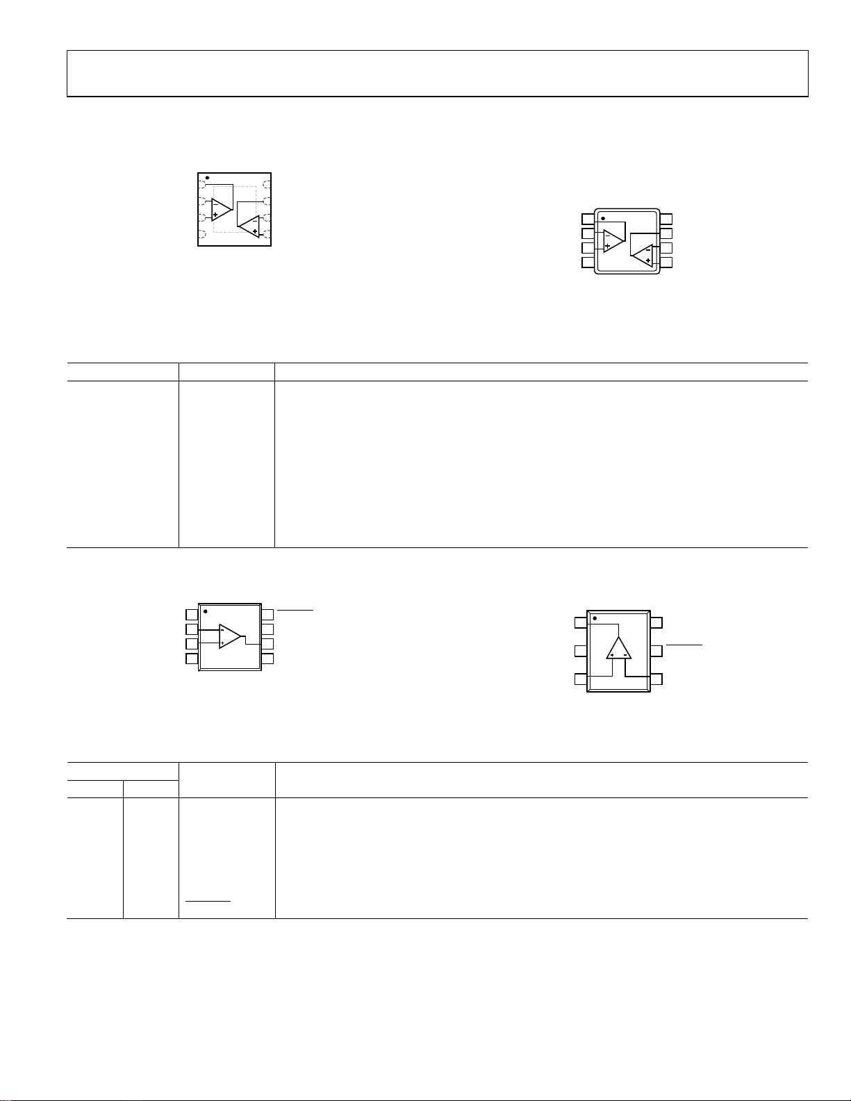
ADA4896-2/ADA4897-1/ADA4897-2
FUNCTIONAL BLOCK DIAGRAM
1
NC
–IN
2
3
+IN
4
V
S
Figure 1. 8-Lead SOIC (ADA4897-1)
8
VS = ±5V
7
6
5
4
3
VOLTAGE NOISE (nV/√Hz)
2
1
0
1 10 100 1k 10k 100k 1M 5M
FREQUENC Y (Hz)
Figure 2. Voltage Noise vs. Frequency
Table 1. Other Low Noise Amplifiers
V
Part No. At 1 kHz At 100 kHz BW (MHz) Voltage (V)
AD797 0.9 0.9 8 10 to 30
AD8021 5 2.1 490 5 to 24
AD8099 3 0.95 510 5 to 12
AD8045 6 3 1000 3.3 to 12
ADA4899-1 1.4 1 600 5 to 12
ADA4898-1/
0.9 0.9 65 10 to 32
ADA4898-2
(nV/√Hz) Supply
N
Table 2. Complementary ADCs
Part No. Bits Speed (MSPS) Power (mW)
AD7944 14 2.5 15.5
AD7985 16 2.5 15.5
AD7986 18 2 15
8
DISABLE
+V
7
6
OUT
NC
5
S
09447-101
09447-102
Rev. B
Information furnished by Analog Devices is believed to be accurate and reliable. However, no
responsibility is assumed by Analog Devices for its use, nor for any infringements of patents or other
rights of third parties that may result from its use. Specifications subject to change without notice. No
license is granted by implication or otherwise under any patent or patent rights of Analog Devices.
Trademarks and registered trademarks are the property of their respective owners.
One Technology Way, P.O. Box 9106, Norwood, MA 02062-9106, U.S.A.
Tel: 781.329.4700 www.analog.com
Fax: 781.461.3113 ©2012 Analog Devices, Inc. All rights reserved.

ADA4896-2/ADA4897-1/ADA4897-2 Data Sheet
TABLE OF CONTENTS
Features .............................................................................................. 1
Applications ....................................................................................... 1
General Description ......................................................................... 1
Functional Block Diagram .............................................................. 1
Revision History ............................................................................... 2
Specifications ..................................................................................... 3
±5 V Supply ................................................................................... 3
+5 V Supply ................................................................................... 4
+3 V Supply ................................................................................... 6
Absolute Maximum Ratings ............................................................ 8
Thermal Resistance ...................................................................... 8
Maximum Power Dissipation ..................................................... 8
ESD Caution .................................................................................. 8
Pin Configurations and Function Descriptions ........................... 9
Typical Performance Characteristics ........................................... 11
Theory of Operation ...................................................................... 17
Amplifier Description ................................................................ 17
Input Protection ......................................................................... 17
Disable Operation ...................................................................... 17
DC Errors .................................................................................... 18
Bias Current Cancellation ......................................................... 18
Noise Considerations ................................................................. 19
Capacitance Drive ...................................................................... 19
Applications Information .............................................................. 20
Typical Performance Values ...................................................... 20
Low Noise, Gain Selectable Amplifier ..................................... 21
Medical Ultrasound Applications ............................................ 22
Layout Considerations ............................................................... 24
Outline Dimensions ....................................................................... 25
Ordering Guide .......................................................................... 27
REVISION HISTORY
4/12—Rev. A to Rev. B
Changed 6-Lead Single SOT-23 (ADA4897-1) Thermal
Reistance from 306°C/W to 150°C/W ........................................... 8
Changes to Figure 3 .......................................................................... 8
10/11—Rev. 0 to Rev. A
Added ADA4897-2 and 10-Lead MSOP ......................... Universal
Change to Table 1 ............................................................................. 1
Changes to Table 3 ............................................................................ 3
Changes to Table 4 ............................................................................ 4
Changes to Table 5 ............................................................................ 6
Changes to Table 7 and Figure 3 ..................................................... 8
Changes to Figure 4, Table 8, and Table 9 ..................................... 9
Added Figure 8 and Table 10; Renumbered Sequentially ......... 10
Changed Summary Statement for Typical Performance
Characteristics Section ................................................................... 11
Changes to Figure 18 ...................................................................... 12
Change to Figure 20 ....................................................................... 12
Change to Figure 26; Moved Figure 26........................................ 13
Changes to Figure 37 ...................................................................... 15
Changes to Amplifier Description Section, Disable Operation
Section, Figure 44, and Figure 45 ................................................. 17
Added Bias Current Cancellation Section, Figure 47,
Table 11, and Table 12 .................................................................... 18
Changes to Table 13 ....................................................................... 20
Changes to Low Noise, Gain Selectable Amplifier Section
and Figure 52 ................................................................................... 21
Deleted Figure 51 ............................................................................ 22
Changes to Power Supply Bypassing Section ............................. 24
Moved Figure 57 ............................................................................. 25
Moved Figure 58 ............................................................................. 26
Added Figure 60 ............................................................................. 27
Changes to Ordering Guide .......................................................... 27
7/11—Revision 0: Initial Version
Rev. B | Page 2 of 28

Data Sheet ADA4896-2/ADA4897-1/ADA4897-2
B
SPECIFICATIONS
±5 V SUPPLY
TA = 25°C, G = +1, RL = 1 kΩ to ground, unless otherwise noted.
Table 3.
Parameter Test Conditions/Comments Min Typ Max Unit
DYNAMIC PERFORMANCE
−3 dB Bandwidth G = +1, V
G = +1, V
G = +2, V
Bandwidth for 0.1 dB Flatness G = +2, V
Slew Rate G = +2, V
Settling Time to 0.1% G = +2, V
Settling Time to 0.01% G = +2, V
NOISE/HARMONIC PERFORMANCE
Harmonic Distortion (SFDR) V
f
f
f
f
OUT
= 100 kHz −115 dBc
C
= 1 MHz −93 dBc
C
= 2 MHz −80 dBc
C
= 5 MHz −61 dBc
C
Input Voltage Noise f = 10 Hz 2.4 nV/√Hz
f = 100 kHz 1 nV/√Hz
Input Current Noise f = 10 Hz 11 pA/√Hz
f = 100 kHz 2.8 pA/√Hz
0.1 Hz to 10 Hz Noise G = +101, RF = 1 kΩ, RG = 10 Ω 99 nV p-p
DC PERFORMANCE
Input Offset Voltage −500 −28 +500 μV
Input Offset Voltage Drift 0.2 μV/°C
Input Bias Current −17 −11 −4 μA
Input Bias Current Drift 3 nA/°C
Input Bias Offset Current −0.6 −0.02 +0.6 μA
Open-Loop Gain V
OUT
INPUT CHARACTERISTICS
Input Resistance
Common-Mode 10 MΩ
Differential 10 kΩ
Input Capacitance
Common-Mode 3 pF
Differential 11 pF
Input Common-Mode Voltage Range −4.9 to +4.1 V
= −2 V to +2 V −92 −120 dB
Common-Mode Rejection Ratio
V
CM
(CMRR)
OUTPUT CHARACTERISTICS
Output Overdrive Recovery Time VIN = ±5 V, G = +2 81 ns
Output Voltage Swing
Positive RL = 1 kΩ 4.85 4.96 V
R
= 100 Ω 4.5 4.73 V
L
Negative RL = 1 kΩ −4.85 −4.97 V
R
= 100 Ω −4.5 −4.84 V
L
Output Current SFDR = −45 dBc 80 mA
Short-Circuit Current Sinking/sourcing 135 mA
Capacitive Load Drive 30% overshoot, G = +2 39 pF
= 0.02 V p-p 230 MHz
OUT
= 2 V p-p 30 MHz
OUT
= 0.02 V p-p 90 MHz
OUT
= 2 V p-p, RL = 100 Ω 7 MHz
OUT
= 6 V step 120 V/μs
OUT
= 2 V step 45 ns
OUT
= 2 V step 90 ns
OUT
= 2 V p-p
= −4 V to +4 V 100 110 dB
Rev. | Page 3 of 28
ADA4896-2/ADA4897-1/ADA4897-2 Data Sheet
B
Parameter Test Conditions/Comments Min Typ Max Unit
POWER SUPPLY
Operating Range 3 to 10 V
Quiescent Current per Amplifier 2.8 3.0 3.2 mA
DISABLE
= −5 V
Power Supply Rejection Ratio (PSRR)
Positive +VS = 4 V to 6 V, −VS = −5 V −96 −125 dB
Negative +VS = 5 V, −VS = −4 V to −6 V −96 −121 dB
DISABLE PIN ( / ) ADA4897-1 ADA4897-2
DISABLE Voltage
Enabled >+V
Disabled <+VS − 2 V
Input Current
Enabled
Disabled
DISABLE
DISABLE
= +5 V
= −5 V
Switching Speed
Enabled 0.25 μs
Disabled 12 μs
+5 V SUPPLY
TA = 25°C, G = +1, RL = 1 kΩ to midsupply, unless otherwise noted.
0.13 0.25 mA
− 0.5 V
S
−1.2 μA
−40 μA
Table 4.
Parameter Test Conditions/Comments Min Typ Max Unit
DYNAMIC PERFORMANCE
−3 dB Bandwidth G = +1, V
G = +1, V
G = +2, V
Bandwidth for 0.1 dB Flatness G = +2, V
Slew Rate G = +2, V
Settling Time to 0.1% G = +2, V
Settling Time to 0.01% G = +2, V
= 0.02 V p-p 230 MHz
OUT
= 2 V p-p 30 MHz
OUT
= 0.02 V p-p 90 MHz
OUT
= 2 V p-p, RL = 100 Ω 7 MHz
OUT
= 3 V step 100 V/μs
OUT
= 2 V step 45 ns
OUT
= 2 V step 95 ns
OUT
NOISE/HARMONIC PERFORMANCE
Harmonic Distortion (SFDR) V
f
f
f
f
= 2 V p-p
OUT
= 100 kHz −115 dBc
C
= 1 MHz −93 dBc
C
= 2 MHz −80 dBc
C
= 5 MHz −61 dBc
C
Input Voltage Noise f = 10 Hz 2.4 nV/√Hz
f = 100 kHz 1 nV/√Hz
Input Current Noise f = 10 Hz 11 pA/√Hz
f = 100 kHz 2.8 pA/√Hz
0.1 Hz to 10 Hz Noise G = +101, RF = 1 kΩ, RG = 10 Ω 99 nV p-p
DC PERFORMANCE
Input Offset Voltage −500 −30 +500 μV
Input Offset Voltage Drift 0.2 μV/°C
Input Bias Current −17 −11 −4 μA
Input Bias Current Drift 3 nA/°C
Input Bias Offset Current −0.6 −0.02 +0.6 μA
Open-Loop Gain V
= 0.5 V to 4.5 V 97 110 dB
OUT
Rev. | Page 4 of 28

Data Sheet ADA4896-2/ADA4897-1/ADA4897-2
B
Parameter Test Conditions/Comments Min Typ Max Unit
INPUT CHARACTERISTICS
Input Resistance
Common-Mode 10 MΩ
Differential 10 kΩ
Input Capacitance
Common-Mode 3 pF
Differential 11 pF
Input Common-Mode Voltage Range 0.1 to 4.1 V
= 1 V to 4 V −91 −118 dB
Common-Mode Rejection Ratio
(CMRR)
OUTPUT CHARACTERISTICS
Output Overdrive Recovery Time VIN = 0 V to 5 V, G = +2 96 ns
Output Voltage Swing
Positive RL = 1 kΩ 4.85 4.98 V
R
Negative RL = 1 kΩ 0.15 0.014 V
R
Output Current SFDR = −45 dBc 70 mA
Short-Circuit Current Sinking/sourcing 125 mA
Capacitive Load Drive 30% overshoot, G = +2 39 pF
POWER SUPPLY
Operating Range 3 to 10 V
Quiescent Current per Amplifier 2.6 2.8 2.9 mA
Power Supply Rejection Ratio (PSRR)
Positive +VS = 4.5 V to 5.5 V, −VS = 0 V −96 −123 dB
Negative +VS = 5 V, −VS = −0.5 V to +0.5 V −96 −121 dB
DISABLE PIN ( / ) ADA4897-1 ADA4897-2
DISABLE Voltage
Disabled <+VS − 2 V
Input Current
Enabled
Disabled
Switching Speed
Enabled 0.25 μs
Disabled 12 μs
V
CM
= 100 Ω 4.8 4.88 V
L
= 100 Ω 0.2 0.08 V
L
DISABLE
= 0 V
0.05 0.18 mA
Enabled >+V
DISABLE
DISABLE
= +5 V
= 0 V
−1.2 μA
−20 μA
− 0.5 V
S
Rev. | Page 5 of 28

ADA4896-2/ADA4897-1/ADA4897-2 Data Sheet
B
+3 V SUPPLY
TA = 25°C, G = +1, RL = 1 kΩ to midsupply, unless otherwise noted.
Table 5.
Parameter Test Conditions/Comments Min Typ Max Unit
DYNAMIC PERFORMANCE
−3 dB Bandwidth G = +1, V
G = −1, V
G = +2, V
Bandwidth for 0.1 dB Flatness G = +2, V
Slew Rate G = +2, V
Settling Time to 0.1% G = +2, V
Settling Time to 0.01% G = +2, V
NOISE/HARMONIC PERFORMANCE
Harmonic Distortion (SFDR) fC = 100 kHz, V
f
f
f
= 1 MHz, V
C
= 2 MHz, V
C
= 5 MHz, V
C
Input Voltage Noise f = 10 Hz 2.3 nV/√Hz
f = 100 kHz 1 nV/√Hz
Input Current Noise f = 10 Hz 11 pA/√Hz
f = 100 kHz 2.8 pA/√Hz
0.1 Hz to 10 Hz Noise G = +101, RF = 1 kΩ, RG = 10 Ω 99 nV p-p
DC PERFORMANCE
Input Offset Voltage −500 −30 +500 μV
Input Offset Voltage Drift 0.2 μV/°C
Input Bias Current −17 −11 −4 μA
Input Bias Current Drift 3 nA/°C
Input Bias Offset Current −0.6 −0.02 +0.6 μA
Open-Loop Gain V
OUT
INPUT CHARACTERISTICS
Input Resistance
Common-Mode 10 MΩ
Differential 10 kΩ
Input Capacitance
Common-Mode 3 pF
Differential 11 pF
Input Common-Mode Voltage Range 0.1 to 2.1 V
= 1.1 V to 1.9 V −90 −124 dB
Common-Mode Rejection Ratio
V
CM
(CMRR)
OUTPUT CHARACTERISTICS
Output Overdrive Recovery Time VIN = 0 V to 3 V, G = +2 83 ns
Output Voltage Swing
Positive RL = 1 kΩ 2.85 2.97 V
R
= 100 Ω 2.8 2.92 V
L
Negative RL = 1 kΩ 0.15 0.01 V
R
= 100 Ω 0.2 0.05 V
L
Output Current SFDR = −45 dBc 60 mA
Short-Circuit Current Sinking/sourcing 120 mA
Capacitive Load Drive 30% overshoot, G = +2 39 pF
POWER SUPPLY
Operating Range 3 to 10 V
Quiescent Current per Amplifier 2.5 2.7 2.9 mA
DISABLE
= 0.02 V p-p 230 MHz
OUT
= 1 V p-p 45 MHz
OUT
= 0.02 V p-p 90 MHz
OUT
= 2 V p-p, RL = 100 Ω 7 MHz
OUT
= 1 V step 85 V/μs
OUT
= 2 V step 45 ns
OUT
= 2 V step 96 ns
OUT
= 2 V p-p, G = +2 −105 dBc
OUT
= 1 V p-p, G = −1 −84 dBc
OUT
= 1 V p-p, G = −1 −77 dBc
OUT
= 1 V p-p, G = −1 −60 dBc
OUT
= 0.5 V to 2.5 V 95 108 dB
= 0 V
0.035 0.15 mA
Rev. | Page 6 of 28
Data Sheet ADA4896-2/ADA4897-1/ADA4897-2
B
Parameter Test Conditions/Comments Min Typ Max Unit
Power Supply Rejection Ratio (PSRR)
Positive +VS = 2.7 V to 3.7 V, −VS = 0 V −96 −121 dB
Negative +VS = 3 V, −VS = −0.3 V to +0.7 V −96 −120 dB
DISABLE PIN ( / ) ADA4897-1 ADA4897-2
DISABLE Voltage
Disabled <−VS + 2 V
Input Current
Enabled
Disabled
Switching Speed
Enabled 0.25 μs
Disabled 12 μs
Enabled >+V
DISABLE
DISABLE
= +3 V
= 0 V
−1.2 μA
−15 μA
− 0.5 V
S
Rev. | Page 7 of 28
ADA4896-2/ADA4897-1/ADA4897-2 Data Sheet
A
ABSOLUTE MAXIMUM RATINGS
Table 6.
Parameter Rating
Supply Voltage 11 V
Power Dissipation See Figure 3
Common-Mode Input Voltage −VS − 0.7 V to +VS + 0.7 V
Differential Input Voltage
0.7 V
Storage Temperature Range −65°C to +125°C
Operating Temperature Range −40°C to +125°C
Lead Temperature (Soldering 10 sec) 300°C
Junction Temperature 150°C
Stresses above those listed under Absolute Maximum Ratings
may cause permanent damage to the device. This is a stress
rating only; functional operation of the device at these or any
other conditions above those indicated in the operational
section of this specification is not implied. Exposure to absolute
maximum rating conditions for extended periods may affect
device reliability.
THERMAL RESISTANCE
θJA is specified for the worst-case conditions, that is, θJA is
specified for a device soldered in a circuit board for surfacemount packages. Table 7 lists the θ
for the ADA4896-2/
JA
ADA4897-1/ADA4897-2.
Table 7. Thermal Resistance
Package Type θJA Unit
8-Lead Dual MSOP (ADA4896-2) 222 °C/W
8-Lead Dual LFCSP (ADA4896-2) 61 °C/W
8-Lead Single SOIC (ADA4897-1) 133 °C/W
6-Lead Single SOT-23 (ADA4897-1) 150 °C/W
10-Lead Dual MSOP (ADA4897-2) 210 °C/W
MAXIMUM POWER DISSIPATION
The maximum safe power dissipation for the ADA4896-2/
ADA4897-1/ADA4897-2 is limited by the associated rise in
junction temperature (T
which is the glass transition temperature, the properties of the
plastic change. Even temporarily exceeding this temperature
limit may change the stresses that the package exerts on the
die, permanently shifting the parametric performance of the
ADA4896-2/ADA4897-1/ADA4897-2. Exceeding a junction
temperature of 175C for an extended period of time can result
in changes in silicon devices, potentially causing degradation or
loss of functionality.
The power dissipated in the package (P
quiescent power dissipation and the power dissipated in the
die due to the ADA4896-2/ADA4897-1/ADA4897-2 drive at
the output.
) on the die. At approximately 150C,
J
) is the sum of the
D
The quiescent power dissipation is the voltage between the supply
pins (±V
RMS output voltages should be considered. If R
−V
I
OUT
case, when V
In single-supply operation with R
is V
Airflow increases heat dissipation, effectively reducing θ
) multiplied by the quiescent current (IS).
S
= Quiescent Power + (Total Drive Power − Load Power)
P
D
V
D
, as in single-supply operation, the total drive power is VS ×
S
IVP
SS
2
V
OUTS
R
L
2
V
OUT
R
L
is referenced to
L
. If the rms signal levels are indeterminate, consider the worst
= VS/4 for RL to midsupply.
OUT
2
V
4/
D
OUT
= VS/2.
IVP
SS
S
R
L
referenced to −VS, worst case
L
.
JA
Also, more metal directly in contact with the package leads
and exposed paddle from metal traces, through holes, ground,
and power planes reduces θ
.
JA
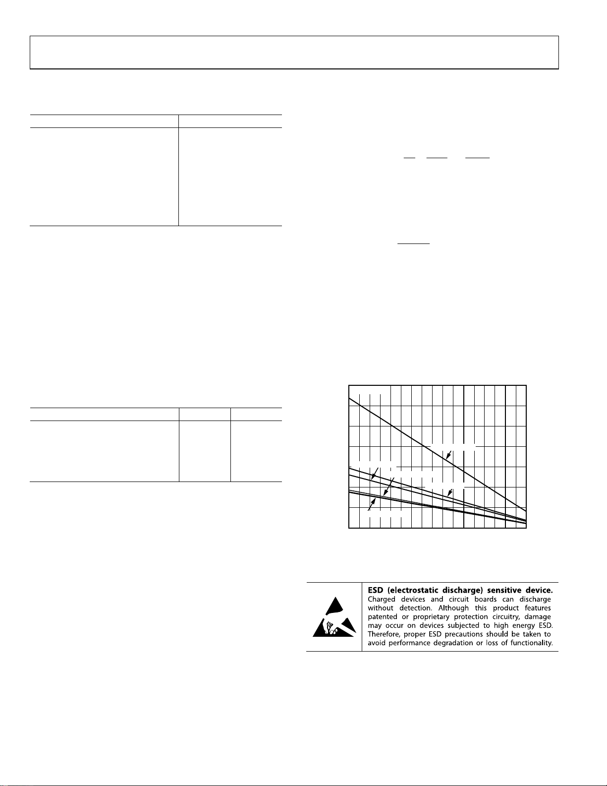
Figure 3 shows the maximum safe power dissipation in the
package vs. the ambient temperature on a JEDEC standard
4-layer board. θ
3.5
3.0
2.5
TION (W)
2.0
1.5
1.0
MAXIMUM POWER DISSIP
0.5
0
–45 –35 –25 –15 –5 5 15 25 35 45 55 65 75 85 95 105 115 125
Figure 3. Maximum Power Dissipation vs. Temperature for a 4-Layer Board
values are approximations.
JA
T
= 150°C
J
6-LEAD SOT-23
10-LEAD MSOP
8-LEAD MSOP
AMBIENT T E M P ERATURE ( ° C)
8-LEAD LF C S P
8-LEAD SOIC
09447-053
ESD CAUTION
Rev. B | Page 8 of 28
Data Sheet ADA4896-2/ADA4897-1/ADA4897-2
T
B
PIN CONFIGURATIONS AND FUNCTION DESCRIPTIONS
ADA4896-2
1OUT1
2–IN1
3+IN1
4–V
S
NOTES
1. THE EXPO SED PAD CAN BE
CONNECTED TO GND OR
POWER PLANES, OR IT CAN
BE LEFT FLOATING.
Figure 4. 8-Lead LFCSP Pin Configuration
Table 8. ADA4896-2 Pin Function Descriptions
Pin No. Mnemonic Description
1 OUT1 Output 1.
2 −IN1 Inverting Input 1.
3 +IN1
4 −V
Negative Supply.
S
5 +IN2
6 −IN2
7 OUT2
8 +V
Positive Supply.
S
EPAD
8+V
S
7OUT2
6–IN2
5+IN2
OUT1
09447-022
–IN1
+IN1
–V
1
2
3
4
S
ADA4896-2
TOP VIEW
(Not to Scale)
8
7
6
5
+V
S
OUT2
–IN2
+IN2
09447-002
Figure 5. 8-Lead MSOP Pin Configuration
Noninverting Input 1.
Noninverting Input 2.
Inverting Input 2.
Output 2.
Exposed Pad (LFCSP Only). The exposed pad can be connected to GND or power planes, or it can
be left floating.
NC
1
–IN
2
+IN
3
4
–V
S
ADA4897-1
NC = NO CONNEC T. DO NOT
CONNEC
8
7
6
5
TO THIS PIN.
DISABLE
+V
S
OUT
NC
09447-016
Figure 6. 8-Lead SOIC Pin Configuration
Table 9. ADA4897-1 Pin Function Descriptions
Pin No.
SOIC Mnemonic Description SOT-23
1, 5 N/A NC No Connect. Do not connect to these pins.
2 4 −IN Inverting Input.
3 3 +IN Noninverting Input.
4 2 −VS Negative Supply.
6 1 OUT Output.
7 6 +VS Positive Supply.
8 5
DISABLE
Disable.
OUT
–V
+IN
1
2
S
3
ADA4897-1
6
+V
5
DISABLE
–IN
4
S
09447-017
Figure 7. 6-Lead SOT-23 Pin Configuration
Rev. | Page 9 of 28

ADA4896-2/ADA4897-1/ADA4897-2 Data Sheet
B
1
OUT1
–IN1
2
+IN1
3
4
–V
S
DISABLE1
ADA4897-2
5
Figure 8. 10-Lead MSOP Pin Configuration
Table 10. ADA4897-2 Pin Function Descriptions
Pin No. Mnemonic Description
1 OUT1 Output 1.
2 −IN1 Inverting Input 1.
3 +IN1 Noninverting Input 1.
4 −VS Negative Supply.
5
6
DISABLE1
DISABLE2
Disable 1.
Disable 2.
7 +IN2 Noninverting Input 2.
8 −IN2 Inverting Input 2.
9 OUT2 Output 2.
10 +VS Positive Supply.
10
+V
OUT2
9
–IN2
8
7
+IN2
DISABLE2
6
S
09447-069
Rev. | Page 10 of 28

Data Sheet ADA4896-2/ADA4897-1/ADA4897-2
B
TYPICAL PERFORMANCE CHARACTERISTICS
RL = 1 kΩ, unless otherwise noted. When G = +1, RF = 0 Ω; otherwise, RF = 249 Ω.
2
VS = +5V
= 20mV p-p
V
OUT
1
0
–1
–2
–3
–4
–5
NORMALIZED CLOSED-L OOP GAIN (dB)
–6
0.1 1 10 100 300
FREQUENCY (MHz)
G = +10
G = –1 OR
G = +2
G = +1
09447-010
Figure 9. Small Signal Frequency Response vs. Gain Figure 12. Frequency Response for Various Output Voltages
2
VS = ±5V
G = +1
1
0
–1
–2
–3
–4
NORMALIZED CLOSED-L OOP GAIN (dB)
–5
0.1 1 10 100 500
100mV p-p
400mV p-p
2V p-p
FREQUENCY (MHz)
20mV p-p
09447-008
2
G = +1
V
= 20mV p-p
OUT
1
0
–1
–2
–3
–4
NORMALIZED CLOSED-L OOP GAIN (dB)
–5
0.1 1 10 100 500
FREQUENCY (MHz)
VS = +5V
VS = ±5V
V
= +3V
S
Figure 10. Small Signal Frequency Response vs. Supply Voltage
2
VS = +5V
G = +1
V
= 20mV p-p
OUT
1
0
–1
–2
–3
–4
NORMALIZ ED CLOSED- LOOP G AIN (dB)
–5
100k 1M 10M 100M 1G
FREQUENCY ( Hz)
–40°C
+125°C
+25°C
Figure 11. Small Signal Frequency Response vs. Temperature
0.8
VS = +5V
= 2V p-p
V
OUT
0.7
G = +2
= 1k
R
L
0.6
0.5
0.4
0.3
0.2
0.1
0
–0.1
NORMALIZ ED CLOSED- LOOP G AIN (dB)
–0.2
–0.3
0.1 1 10 50
09447-005
FREQUENCY ( MHz)
Figure 13. 0.1 dB Bandwidth at Selected R
2
VS = +5V
= 2V p-p
V
OUT
1
0
–1
–2
–3
–4
–5
NORMALIZ ED CLOSE D-LOOP GAIN (dB)
–6
0.1 1 10 100
09447-038
FREQUENC Y (MHz)
RF = RG = 249
RF = RG = 100
RF = RG = 49.9
G = +10
Values
F
G = –1
G = +1
09447-061
09447-006
Figure 14. Large Signal Frequency Response vs. Gain
Rev. | Page 11 of 28

ADA4896-2/ADA4897-1/ADA4897-2 Data Sheet
–
–
–
–
–
B
4
VS = +5V
3
G = +2
R
= 100
L
V
OUT
= 20mV p-p
C
L
= 39pF
2
1
0
C
L
= 20pF
–1
= 0pF
C
–2
NORMALIZED CL OSED-LOOP GAIN (dB)
–3
0.1 1 10 100
L
FREQUENCY ( MHz)
Figure 15. Small Signal Frequency Response vs. Capacitive Load
09447-007
30
V
= +5V
S
V
= 2V p-p
OUT
G = +10
–40
RL = 100, SECOND
–50
–60
–70
–80
DISTORTION (dBc)
–90
–100
–110
0.1 1
RL = 1k, SECOND
RL = 100, THIRD
RL = 1k, THIRD
FREQUENCY ( MHz)
Figure 18. Harmonic Distortion vs. Frequency, G = +10
5
09447-070
50
VS = +5V
V
= 2V p-p
OUT
G = +1
–60
–70
RL = 100, SECOND
–80
RL = 100, THIRD
–90
DISTORTION (dBc)
–100
–110
–120
0.1 1 5
RL = 1k, THIRD
RL = 1k, SECOND
FREQUENCY (MHz)
Figure 16. Harmonic Distortion vs. Frequency, G = +1
40
= +5V
V
S
= 2V p-p
V
OUT
G = +5
–50
RL = 100, SECOND
–60
–70
–80
DISTORTION (dBc)
–90
RL = 100, THIRD
RL = 1k, THIRD
–100
RL = 1k, SECOND
–110
0.1 1
FREQUENC Y (MHz)
Figure 17. Harmonic Distortion vs. Frequency, G = +5
50
V
= ±5V
S
G = +1
R
= 1k
–60
L
–70
–80
8V p-p, THIRD
–90
8V p-p, SECOND
DISTORT ION (dBc)
–100
–110
–120
0.1 1
09447-021
FREQUENCY (MHz)
2V p-p, SECOND
2V p-p, THIRD
4V p-p, SECO ND
4V p-p, THIRD
5
09447-026
Figure 19. Harmonic Distortion vs. Frequency for Various Output Voltages
50
–60
–70
G = +2
R
= 1k
L
VS = +5V,
THIRD
VS = +5V,
SECOND
–80
VS = +3V,
–90
SECOND
–100
DISTORTION (dBc)
–110
–120
–130
5
09447-041
0.1 1 5
VS = +3V,
THIRD
FREQUENCY (MHz)
VS = ±5V,
THIRD
VS = ±5V,
SECOND
09447-045
Figure 20. Harmonic Distortion vs. Frequency for Various Supplies
Rev. | Page 12 of 28

Data Sheet ADA4896-2/ADA4897-1/ADA4897-2
–
B
90
80
70
60
50
GAIN
PHASE
40
30
20
OPEN-LOOP GAIN (dB)
10
0
–10
–20
10k 100k 1M 10M 100M 1G
FREQUENCY (Hz)
Figure 21. Open-Loop Gain and Phase vs. Frequency
80
–100
–120
–140
–160
–180
–200
–220
–240
OPEN-LO OP PHASE (Degrees)
09447-044
18
VS = ±5V
100 UNITS
16
= 309.2µV/°C
14
12
10
8
6
NUMBER OF PARTS
4
2
0
–600 –400 –200 0 200 400 600 800 1000
OFFSET VOLTAG E DRIFT DI STRIBUTI ON (nV/° C)
Figure 24. Input Offset Voltage Drift Distribution
09447-066
8
7
6
VS = ±5V
V
= +3V
S
VS = +5V
10
= ±5V
V
S
G = +1
= 20mV p-p
V
OUT
TIME = 100n s/DIV
5
4
0
3
VOLTAGE NOISE (nV/Hz)
2
OUTPUT VOLTAGE (mV)
–10
1
09447-050
0
1
100
Hz)
10
100
10
10k 100k 1M
1k
FREQUENC Y (Hz)
Figure 22. Voltage Noise vs. Frequency
V
= ±5V
S
5M
09447-027
Figure 25. Small Signal Transient Response for Various Supplies, G = +1
VS = +3V
= +5V
V
V
S
= ±5V
S
10
0
G = +2
V
= 20mV p-p
OUT
TIME = 100n s/DIV
CURRENT NOISE (pA/
OUTPUT VOLTAGE (mV)
–10
9447-040
1
1 10 100
Figure 23. Current Noise vs. Frequency
1k 10k 100k 1M 5M
FREQUENCY (Hz)
09447-060
Figure 26. Small Signal Transient Response for Various Supplies, G = +2
Rev. | Page 13 of 28

ADA4896-2/ADA4897-1/ADA4897-2 Data Sheet
B
CL = 39pF
CL = 20pF
CL = 0pF
VS = ±5V
G = +2
TIME = 100ns/DIV
10
3
2
2× V
IN
V
OUT
VS = +5V
G = +2
TIME = 100ns/DIV
1
0
OUTPUT VOL TAGE (mV)
–10
09447-039
Figure 27. Small Signal Transient Response for Various Capacitive Loads
1.5
G = +2
1.0
G = +1
0.5
0
–0.5
OUTPUT VOLTAGE (V)
–1.0
–1.5
VS = ±5V
= 2V p-p
V
OUT
TIME = 100ns/DIV
09447-009
Figure 28. Large Signal Transient Response, G = +1 and G = +2
0
–1
–2
INPUT AND OUTPUT VOLT AGE (V)
–3
09447-051
Figure 30. Output Overdrive Recovery Time
250
VS = +5V
G = +2
200
150
100
50
0
AVERAGE OUT PUT OVERL OAD RECOVERY TIME (n s)
0 100 200 300 400 500 600 700 800 900
OVERLOAD DURAT ION (ns)
09447-055
Figure 31. Average Output Overload Recovery Time vs. Overload Duration
4
3
V
IN
VS = +5V
G = +1
TIME = 100n s/DIV
2
1
V
OUT
0
–1
–2
INPUT AND OUTP UT VOLT AGE (V)
–3
–4
09447-049
Figure 29. Input Overdrive Recovery Time
105.0
102.5
100.0
RISING EDG E
V
OUT
V
= +5V
S
G = +2
97.5
95.0
FALLING EDGE
92.5
90.0
SLEW RATE (V/µs)
87.5
85.0
82.5
80.0
–40 –25 –10 5 20 35 50 65 80 95 110 125
TEMPERATURE (°C)
Figure 32. Slew Rate vs. Temperature
= 3V p-p
09447-052
Rev. | Page 14 of 28

Data Sheet ADA4896-2/ADA4897-1/ADA4897-2
–
–
–
B
0.3
0.2
VS = +5V
G = +2
V
= 2V STEP
OUT
R
= 1k
L
TIME = 10ns/DIV
0.1
0
–0.1
SETTLING TIME (%)
–0.2
100000
10000
1000
100
OUTPUT IM PEDANCE ()
0.1
VS = +5V
G = +1
P
= –30dBm
PART DISABLED
10
PART ENABLED
1
IN
CMRR (dB)
PSRR (dB)
–30
–40
–50
–60
–70
–80
–90
–100
–110
–120
–130
–10
–20
–30
–40
–50
–60
–70
–80
–90
–100
–110
–120
–130
–0.3
20
VS = +5V
V
0
= 2V p-p
CM
VS = +5V
= 2V p-p
V
S
G = +1
Figure 33. Settling Time to 0.1%
1M 10M
FREQUENCY (Hz)
Figure 34. CMRR vs. Frequency
–PSRR
+PSRR
1M 10M
FREQUENCY (Hz)
Figure 35. PSRR vs. Frequency
09447-028
0.01
0.1 1 10 100 500
FREQUENCY (MHz)
09447-013
Figure 36. Output Impedance vs. Frequency
26.0
VS = ±5V
–28.5
VS = +5V
VS = +3V
–31.0
INPUT OFFSET VOLTAGE (µV)
–33.5
100M100k10k1k
09447-029
–40 –25 –10 5 20 35 50 65 80 95 110 125
TEMPERATURE (° C)
09447-042
Figure 37. Input Offset Voltage vs. Temperature for Various Supplies
10.50
VS = ±5V
–10.75
VS = +5V
–11.00
VS = +3V
–11.25
INPUT BIAS CURRENT (µA)
100M100k10k1k
09447-030
–11.50
–40 –25 –10 5 20 35 50 65 80 95 110 125
TEMPERAT URE (°C)
09447-046
Figure 38. Input Bias Current vs. Temperature for Various Supplies
Rev. | Page 15 of 28

ADA4896-2/ADA4897-1/ADA4897-2 Data Sheet
–
–
B
3.2
3.1
3.0
2.9
2.8
2.7
SUPPLY CURRENT (mA)
2.6
2.5
–40 –25 –10 5 20 35 50 65 80 95 110 125
VS = ±5V
VS = +5V
= +3V
V
S
TEMPERATURE (°C)
Figure 39. Supply Current vs. Temperature for Various Supplies
09447-043
5.5
5.0
4.5
4.0
3.5
3.0
2.5
2.0
DISABLE PIN (V)
1.5
1.0
0.5
–0.5
DISABLE PIN
0
+25°C
+125°C
–40°C
TIME = 2µs/DIV
V
= +5V
S
G = +1
V
= 1V
IN
3.875
3.750
3.625
3.500
3.375
3.250
3.125
3.000
2.875
2.750
2.625
2.500
2.375
Figure 42. Turn-Off Time vs. Temperature (ADA4897-1 and ADA4897-2)
OUTPUT VOLTAGE (V)
09447-056
40
VS = +5V
G = +2
CROSSTALK (dB)
–50
–60
–70
–80
–90
–100
–110
–120
–130
= 2V p-p
V
OUT
0.01 0.1 1 10
FREQUENCY (MHz)
Figure 40. Crosstalk, OUT1 to OUT2 (ADA4896-2 and ADA4897-2)
5.5
5.0
4.5
4.0
3.5
3.0
2.5
2.0
DISABLE PIN (V)
1.5
1.0
0.5
0
–0.5
DISABLE PIN
+25°C
–40°C
TIME = 200ns/DIV
V
= +5V
S
G = +1
V
= 1V
IN
+125°C
Figure 41. Turn-On Time vs. Temperature (ADA4897-1 and ADA4897-2)
100
3.875
3.750
3.625
3.500
3.375
3.250
3.125
3.000
2.875
2.750
2.625
2.500
2.375
30
VS = +5V
G = +2
–40
R
= 100
L
V
= 2V p-p
OUT
–50
–60
–70
–80
–90
–100
ISOLAT ION (d B)
–110
–120
–130
–140
0.01 0.1 1 10
09447-014
FREQUENCY (MHz)
100
09447-015
Figure 43. Forward Isolation vs. Frequency
OUTPUT VOLTAGE (V)
09447-054
Rev. | Page 16 of 28

Data Sheet ADA4896-2/ADA4897-1/ADA4897-2
V
V
B
THEORY OF OPERATION
AMPLIFIER DESCRIPTION
The ADA4896-2/ADA4897-1/ADA4897-2 are 1 nV/√Hz input
noise amplifiers that consume 3 mA from supplies ranging from
3 V to 10 V. Fabricated on the Analog Devices SiGe bipolar process,
the ADA4896-2/ADA4897-1/ADA4897-2 have a bandwidth in
excess of 200 MHz. The amplifiers are unity-gain stable, and the
input structure results in an extremely low input 1/f noise for a
high speed amplifier.
The rail-to-rail output stage is designed to drive the heavy feedback load required to achieve an overall low output referred noise.
To meet more demanding system requirements, the large signal
bandwidth of the ADA4896-2/ADA4897-1/ADA4897-2 was
increased beyond the typical fundamental limits of other low noise,
unity-gain stable amplifiers. The maximum offset voltage of 500 μV
and drift of 0.2 μV/°C make the ADA4896-2/ADA4897-1/
ADA4897-2 excellent amplifier choices even when the low noise
performance is not needed because there is minimal power
penalty in achieving the low input noise or the high bandwidth.
INPUT PROTECTION
The ADA4896-2/ADA4897-1/ADA4897-2 are fully protected
from ESD events, withstanding human body model ESD events
of 2.5 kV and charged-device model events of 1 kV with no measured performance degradation. The precision input is protected
with an ESD network between the power supplies and diode
clamps across the input device pair, as shown in Figure 44.
+
S
BIAS
ESD
+IN
ESD
–V
S
TO THE REST OF THE AMPLIFIER
Figure 44. Input Stage and Protection Diodes
For differential voltages above approximately 0.7 V, the diode
clamps begin to conduct. Too much current can cause damage
due to excessive heating. If large differential voltages must be
sustained across the input terminals, it is recommended that the
current through the input clamps be limited to less than 10 mA.
Series input resistors that are sized appropriately for the expected
differential overvoltage provide the needed protection.
ESD
ESD
–IN
09447-068
The ESD clamps begin to conduct for input voltages that are
more than 0.7 V above the positive supply and input voltages
more than 0.7 V below the negative supply. If an overvoltage
condition is expected, it is recommended that the input current
be limited to less than 10 mA.
DISABLE OPERATION
Figure 45 shows the ADA4897-1/ADA4897-2 power-down
circuitry. If the
DISABLE
the input PNP transistor is pulled high through the internal
pull-up resistor to the positive supply and the part is turned
on. Pulling the
DISABLE
turns the part off, reducing the supply current to approximately
18 μA for a 5 V voltage supply.
+
S
–V
S
DISABLE
The
pin is protected by ESD clamps, as shown in
Figure 45. Voltages beyond the power supplies cause these
diodes to conduct. For protection of the
voltage to this pin should not exceed 0.7 V above the positive
supply or 0.7 V below the negative supply. If an overvoltage
condition is expected, it is recommended that the input current
be limited with a series resistor to less than 10 mA.
When the amplifier is disabled, its output goes to a high
impedance state. The output impedance decreases as frequency
increases; this effect can be observed in Figure 36. In disable
mode, a forward isolation of 50 dB can be achieved at 10 MHz.
Figure 43 shows the forward isolation vs. frequency data.
pin is left unconnected, the base of
pin to ≥2 V below the positive supply
I
BIAS
ESD
DISABLE
ESD
TO
AMPLIFIER
BIAS
DISABLE
Figure 45.
Circuit
DISABLE
pin, the
09447-037
Rev. | Page 17 of 28

ADA4896-2/ADA4897-1/ADA4897-2 Data Sheet
V
B
DC ERRORS
Figure 46 shows a typical connection diagram and the major
dc error sources.
R
F
– VIN +
R
G
– VIP +
R
S
Figure 46. Typical Connection Diagram and DC Error Sources
The ideal transfer function (all error sources set to 0 and
infinite dc gain) can be written as
⎛
OUT
⎜
+= 1
⎜
⎝
V ×
This equation reduces to the familiar forms for noninverting
and inverting op amp gain expressions, as follows:
For noninverting gain (V
⎛
OUT
⎜
1
+=
⎜
⎝
V
For inverting gain (V
⎛
R
−
OUT
⎜
=
⎜
R
⎝
V ×
The total output voltage error is the sum of errors due to the
amplifier offset voltage and input currents. The output error
due to the offset voltage can be estimated as
=
OUT
ERROR
⎛
⎜
⎝
V
OFFSET
NOM
V
CM
CMRR
where:
V
OFFSET
is the offset voltage at the specified supply voltage,
NOM
which is measured with the input and output at midsupply.
V
is the common-mode voltage.
CM
is the power supply voltage.
V
P
is the specified power supply voltage.
V
PNOM
CMRR is the common-mode rejection ratio.
PSRR is the power supply rejection ratio.
A is the dc open-loop gain.
G
R
R
R
R
F
⎞
F
⎟
⎟
G
⎠
⎞
F
⎟
⎟
G
⎠
IP
⎞
⎟
⎟
⎠
++
+ VOS –
+ V
–
–
I
B
IB+
⎞
⎛
R
F
⎟
⎜
V
−×
IN
V
×
IP
= 0 V)
IP
⎟
⎜
R
G
⎠
⎝
(2)
OUT
09447-031
(1)
V
IN
= 0 V)
V
(3)
IN
−
P
PSRR
VV
V
OUTPNOM
+
⎛
⎞
⎜
⎟
⎜
A
⎠
⎝
⎞
R
F
⎟
+×
1
⎟
R
G
⎠
(4)
The output error due to the input currents can be estimated as
OUT
ERROR
⎛
⎜
RRV
F
G
⎜
⎝
⎞
R
F
⎟
+×=
B
⎟
R
G
⎠
⎛
⎜
RI
S
⎜
⎝
⎞
R
F
⎟
(5)
×
+×−×
11)||(
I
+−
B
⎟
R
G
⎠
BIAS CURRENT CANCELLATION
To cancel the output voltage error due to unmatched bias
currents at the inputs, R
R
R
Figure 47. Using R
To compensate for the unmatched bias currents at the two
inputs, set R
and RBN as shown in Table 11.
BP
Table 11. Setting RBN and RBP to Cancel Bias Current Errors
Value of RF||RG Value of RBP (Ω) Value of RBN (Ω)
Greater Than RS R
Less Than RS 0 RS − RF||RG
Table 12 shows sample values for RBP and RBN when RF||RG > RS
and when R
||RG < RS.
F
Table 12. Examples of RBN and RBP Settings
Gain RF (Ω) RG (Ω) RS (Ω) RBP (Ω) RBN (Ω)
+2 249 249 50 74.5 0
+10 249 27.4 50 0 25.3
and RBN can be used (see Figure 47).
BP
G
S
and RBN to Cancel Bias Current Error
BP
||RG − RS 0
F
R
F
R
BN
R
BP
09447-048
Rev. | Page 18 of 28

Data Sheet ADA4896-2/ADA4897-1/ADA4897-2
=
√
B
NOISE CONSIDERATIONS
500
Figure 48 illustrates the primary noise contributors for the
typical gain configurations. The total rms output noise is
the root-mean-square of all the contributions.
vn _ RF
F
4kT × R
F
+ vout_en –
09447-034
vn _ RG =
vn _ RS =
R
4kT × R
4kT × R
R
G
G
R
S
S
ven
ien
iep
Figure 48. Noise Sources in Typical Connection
The output noise spectral density can be calculated by
_
envout
=
2
⎞
⎛
R
F
⎟
⎜
+++
4414
⎟
⎜
R
G
⎠
⎝
2
2
RienkTR
+
FG
kTR
2
⎞
⎛
R
F
⎟
⎜
F
⎜
⎝
[]
++
⎟
R
G
⎠
2
2
2
venRiepkTRs
S
(6)
where:
k is Boltzmann’s constant.
T is the absolute temperature (degrees Kelvin).
iep
ien
and
represent the amplifier input current noise spectral
density (pA/√Hz).
ven
is the amplifier input voltage noise spectral density (nV/√Hz).
R
is the source resistance, as shown in Figure 48.
S
R
and RG are the feedback network resistances, as shown in
F
Figure 48.
50
Hz)
NOISE (n V/
5
0.5
50 500
AMPLIFIER AND
RESISTOR NOISE
RESISTANCE NOISE
TOTAL
AMPLIFI ER NOISE
SOURCE RESIS TANCE (Ω)
SOURCE
5k 50k
Figure 49. RTI Noise vs. Source Resistance
CAPACITANCE DRIVE
Capacitance at the output of an amplifier creates a delay within the
feedback path that, if within the bandwidth of the loop, can create
excessive ringing and oscillation. The ADA4896-2/ADA4897-1/
ADA4897-2 show the most peaking at a gain of +2 (see Figure 9).
Placing a small snub resistor (R
output and the capacitive load mitigates the problem. Figure 50
shows the effect of using a snub resistor (R
peaking for the worst-case frequency response (gain of +2).
Using R
= 100 eliminates the peaking entirely, with the
SNUB
trade-off that the closed-loop gain is reduced by 0.8 dB due to
attenuation at the output. R
) in series with the amplifier
SNUB
) on reducing the
SNUB
can be adjusted from 0 to
SNUB
100 to maintain an acceptable level of peaking and closed-
Source resistance noise, amplifier voltage noise (
voltage noise from the amplifier current noise (
subject to the noise gain term (1 + R
). Note that with a
F/RG
1 nV/√Hz input voltage noise and 2.8 pA/√Hz input current
noise, the noise contributions of the amplifier are relatively
small for source resistances from approximately 50 Ω to 700 Ω.
ven
), and the
iep
× RS) are all
loop gain (see Figure 50).
3
VS = +5V
V
= 200mV p-p
OUT
2
G = +2
1
= 100Ω
R
SNUB
0
R
SNUB
= 50Ω
R
SNUB
= 0Ω
Figure 49 shows the total RTI noise due to the amplifier vs. the
source resistance. In addition, the value of the feedback resistors
used affects the noise. It is recommended that the value of the
feedback resistors be maintained between 250 Ω and 1 kΩ to
keep the total noise low.
–1
–2
–3
–4
NORMALIZE D CLOSED-LOOP GAIN (dB)
–5
0.1 1 10 100
R
249Ω
V
IN
1
R
2
249Ω
ADA4896-2
FREQUENCY (MHz)
R
SNUB
V
R
1kΩ
L
OUT
C
L
39pF
Figure 50. Using a Snub Resistor to Reduce Peaking
Due to Output Capacitive Load
09447-057
09447-058
Rev. | Page 19 of 28

ADA4896-2/ADA4897-1/ADA4897-2 Data Sheet
B
APPLICATIONS INFORMATION
2
TYPICAL PERFORMANCE VALUES
To reduce design time and eliminate uncertainty, Table 1 3
provides a reference for typical gains, component values, and
performance parameters. The supply voltage used is 5 V. The bandwidth is obtained with a small signal output of 200 mV p-p, and
the slew rate is obtained with a 2 V output step.
Note that as the gain increases, the small signal bandwidth
decreases, as is expected from the gain bandwidth product
relationship. In addition, the phase margin improves with
higher gains, and the amplifier becomes more stable. As a
result, the peaking in the frequency response is reduced
(see Figure 51).
Table 13. Recommended Values and Typical Performance
Gain RF (Ω) RG (Ω) −3 dB BW (MHz) Slew Rate, tR/tF (V/μs) Peaking (dB)
+1 0 N/A 92 78/158 0.8 1.0
+2 249 249 54 101/140 1.2 3.6
+5 249 61.9 30 119/137 0 6.8
+10 249 27.4 17 87/88 0 12.0
+20 249 13.0 9 37/37 0 21.1
VS = +5V
V
= 200mV p-p
OUT
1
R
= 249
F
R
= 1k
L
0
–1
–2
–3
–4
–5
NORMALIZE D CLOSED-LO OP GAIN (d B)
–6
0.1 1 10 100 500
G = +10
G = +20
FREQUENCY (MHz)
G = +5
G = +2
G = +1
Figure 51. Small Signal Frequency Response at Various Gains
Total Output Noise Including
Resistors (nV/√Hz)
09447-020
Rev. | Page 20 of 28

Data Sheet ADA4896-2/ADA4897-1/ADA4897-2
B
LOW NOISE, GAIN SELECTABLE AMPLIFIER
R
F2
225
R
F1
75
R
G1
75
V
IN
+5V
8
2
ADA4896-2
3
4
–5V
S1B
V1
D1 D2
1
V
01
S1A
V2
Figure 52. Using the ADA4896-2 and the ADG633 to Construct a Low Noise, Gain Selectable Amplifier to Drive a Low Resistive Load
A gain selectable amplifier makes processing a wide range of
input signals possible. A traditional gain selectable amplifier
uses switches in the feedback loops connecting to the inverting
input. The switch resistances degrade the noise performance of
the amplifier, as well as adding significant capacitance on the
inverting input node. The noise and capacitance issues can be
especially bothersome when working with low noise amplifiers.
Also, the switch resistances contribute to nonlinear gain error,
which is undesirable.
Figure 52 presents an innovative switching technique used in
the gain selectable amplifier such that the 1 nV/Hz noise performance of the ADA4896-2 is preserved while the nonlinear
gain error is much reduced. With this technique, the user can
also choose switches with minimal capacitance to optimize the
bandwidth of the circuit.
In the circuit shown in Figure 52, the switches are implemented
with the ADG633 and are configured such that either S1A and
S2A are on, or S1B and S2B are on. In this example, when the
S1A and S2A switches are on, the first stage amplifier gain is +4.
When the S1B and S2B switches are on, the first stage amplifier
gain is +2. The first set of switches of the ADG633 is placed on
the output side of the feedback loop, and the second set of switches
is used to sample at a point (V1 or V2) where switch resistances
and nonlinear resistances do not matter. In this way, the gain
error can be reduced while preserving the noise performance
of the ADA4896-2.
Note that the input bias current of the output buffer can cause
problems with the impedance of the S2A and S2B sampling
switches. Both sampling switches are not only nonlinear with
voltage but with temperature as well. If this is an issue, place the
unused switch of the ADG633 (S3B) in the feedback path of the
output buffer to balance the bias currents (see Figure 52).
In addition, the bias current of the input amplifier causes
an offset at the output that varies based on the gain setting.
Because the input amplifier and the output buffer are monolithic, the relative matching of their bias currents can be used
R
BALANCE
150
ADG633
to cancel out the varying offset. Placing a resistor equal to the
difference between R
in a more constant offset voltage.
The following derivation shows that sampling at V1 yields the
desired signal gain without gain error. R
resistance. V2 can be derived using the same method.
Substituting Equation 1 into Equation 2, the following
derivation is obtained.
Note that if V
error, the buffered output V
error. Figure 53 shows the normalized frequency response of
the circuit at V
USING S3B IS OPTIONAL
S3B D3
+5V
8
6
S2B
S2A
NORMALIZED CLOSED-LOOP GAIN (dB)
ADA4896-2
5
4
–5V
⎛
⎜
VV 1
01
IN
⎜
⎝
⎛
⎜
×=
VV1
01
⎜
⎝
⎛
⎜
VV1 1
IN
⎜
⎝
yields the desired signal gain without gain
01
.
02
6
VS = ±5V
V
= 100mV p-p
3
IN
R
= 1k
L
0
–3
–6
–9
–12
–15
–18
–21
–24
–27
–30
0.1 1 10 100 500
Figure 53. Frequency Response of V
ADG633
7
V
02
R
L
09447-100
and RF1 in series with Switch S2A results
F2
denotes the switch
S
⎞
RR
+
F1
S1
+×=
F1
F1
R
F1
+×=
R
G1
⎟
(7)
⎟
R
G1
⎠
+
⎞
⎟
⎟
⎠
FREQUENCY (MHz)
⎞
RR
G1
⎟
(8)
⎟
++
RRR
S1G1
⎠
(9)
will also be free from gain
02
G = +4
02/VIN
G = +2
09447-064
Rev. | Page 21 of 28

ADA4896-2/ADA4897-1/ADA4897-2 Data Sheet
B
MEDICAL ULTRASOUND APPLICATIONS
HV
TRANSDUCER
ARRAY
MUX/
DEMUX
T/R
SWITCHES
CW (ANALOG)
BEAMFORMER
ADA4896-2/
ADA4897-1/
ADA4897-2
Figure 54. Simplified Ultrasound System Block Diagram
Overview of the Ultrasound System
Medical ultrasound systems are among the most sophisticated
signal processing systems in widespread use today. By transmitting acoustic energy into the body and receiving and processing
the returning reflections, ultrasound systems can generate images
of internal organs and structures, map blood flow and tissue
motion, and provide highly accurate blood velocity information.
Figure 54 shows a simplified block diagram of an ultrasound
system.
AD9279
AUDIO
OUTPUT
Tx BEAMFORMER
VGALNA
AAF
SPECTRAL
DOPPLER
PROCESSING
MODE
ADC
BEAMFORMER
CENTRAL CONTROL
Rx BEAMFORMER
(B AND F MODES)
IMAGE AND
MOTION
PROCESSING
(B MODE)
DISPLAY
COLOR
DOPPLER
PROCESSING
(F MODE)
The ultrasound system consists of two main operations: the
time gain control (TGC) operation and the continuous wave
(CW) Doppler operation. The AD9279 integrates the essential
components of these two operations into a single IC. It contains
eight channels of a variable gain amplifier (VGA) with a low
noise preamplifier (LNA), an antialiasing filter (AAF), an
analog-to-digital converter (ADC), and an I/Q demodulator
with programmable phase rotation. For detailed information
about how to use the AD9279 in an ultrasound system, see the
AD9279 data sheet.
09447-033
Rev. | Page 22 of 28

Data Sheet ADA4896-2/ADA4897-1/ADA4897-2
A
B
ADA4896-2/ADA4897-1/ADA4897-2 in the Ultrasound System
R
FILT
C
FILT
R
CHANNEL
CHANNEL H
LNA
LNA
4
LO
GENERATI ON
AD9279
CWI+
CWI–
CWQ+
CWQ–
1.5V
1.5V
R
R
1.5V
1.5V
R
A
ADA4896-2/
ADA4897-1/
ADA4897-2
A
C
FILT
R
FILT
R
FILT
C
FILT
A
ADA4896-2/
ADA4897-1/
ADA4897-2
A
C
FILT
R
FILT
2.5V
2.5V
2.5V
2.5V
50
ADA4896-2/
ADA4897-1/
ADA4897-2
50
50
ADA4896-2/
ADA4897-1/
ADA4897-2
50
4nF
4nF
AD7982
18-BIT ADC
AD7982
18-BIT ADC
I
Q
4LO–
4LO+
RESET
Figure 55. Using the ADA4896-2/ADA4897-1/ADA4897-2 as Filters, I-to-V Converters, Current Summers, and ADC Drivers After the I/Q Outputs of the AD9279
The ADA4896-2/ADA4897-1/ADA4897-2 are used in the CW
Doppler path in the ultrasound application after the I/Q demodulators of the AD9279. Doppler signals can be typically between
100 Hz to 100 kHz. The low noise floor and high dynamic range
of the ADA4896-2/ADA4897-1/ADA4897-2 make them excellent
choices for processing weak Doppler signals.
The rail-to-rail output and the high output current drive of
the ADA4896-2/ADA4897-1/ADA4897-2 make them suitable
candidates for the I-to-V converter, current summer, and ADC
driver.
Figure 55 shows an interconnection block diagram of all
eight channels of the AD9279. Two stages of the ADA4896-2
amplifiers are used. The first stage performs an I-to-V conversion and filters the high frequency content that results from
the demodulation process. The second stage of the ADA4896-2
amplifiers is used to sum the output currents of multiple AD9279
The output-referred noise of the CW signal path depends on
the LNA gain, the selection of the first stage summing amplifier,
and the value of R
. To determine the output-referred noise, it
FILT
is important to know the active low-pass filter (LPF) values R
R
FILT
, and C
, as shown as Figure 55. Typical filter values for
FILT
all eight channels of a single AD9279 are 100 Ω for R
for R
, and 2.0 nF for C
FILT
; these values implement a 100 kHz,
FILT
single-pole LPF.
The gain of the I-to-V converter can be increased by increasing
the filter resistor, R
decrease the filter capacitor, C
. To keep the corner frequency unchanged,
FILT
, by the same factor. The factor
FILT
limiting the magnitude of the gain is the output swing and drive
capability of the op amp selected for the I-to-V converter, in this
example, the ADA4896-2/ADA4897-1/ADA4897-2. Because
any amplifier has limited drive capability, a finite number of
channels can be summed.
devices, to provide gain, and to drive the AD7982 device, an
18-bit SAR ADC.
09447-032
, 500 Ω
A
,
A
Rev. | Page 23 of 28

ADA4896-2/ADA4897-1/ADA4897-2 Data Sheet
B
LAYOUT CONSIDERATIONS
To ensure optimal performance, careful and deliberate attention
must be paid to the board layout, signal routing, power supply
bypassing, and grounding.
Ground Plane
It is important to avoid ground in the areas under and around the
input and output of the ADA4896-2/ADA4897-1/ADA4897-2.
Stray capacitance created between the ground plane and the
input and output pads of a device is detrimental to high speed
amplifier performance. Stray capacitance at the inverting input,
along with the amplifier input capacitance, lowers the phase
margin and can cause instability. Stray capacitance at the output
creates a pole in the feedback loop, which can reduce phase margin
and can cause the circuit to become unstable.
Power Supply Bypassing
Power supply bypassing is a critical aspect in the performance
of the ADA4896-2/ADA4897-1/ADA4897-2. A parallel connec-
tion of capacitors from each power supply pin to ground works
best. Smaller value capacitor electrolytics offer better high
frequency response, whereas larger value capacitor electrolytics
offer better low frequency performance.
Paralleling different values and sizes of capacitors helps to ensure
that the power supply pins are provided with a low ac impedance
across a wide band of frequencies. This is important for minimizing the coupling of noise into the amplifier—especially when the
amplifier PSRR begins to roll off—because the bypass capacitors
can help lessen the degradation in PSRR performance.
The smallest value capacitor should be placed on the same side
of the board as the amplifier and as close as possible to the amplifier power supply pins. The ground end of the capacitor should
be connected directly to the ground plane.
It is recommended that a 0.1 μF ceramic capacitor with a 0508
case size be used. The 0508 case size offers low series inductance
and excellent high frequency performance. A 10 μF electrolytic
capacitor should be placed in parallel with the 0.1 μF capacitor.
Depending on the circuit parameters, some enhancement to
performance can be realized by adding additional capacitors.
Each circuit is different and should be analyzed individually for
optimal performance.
Rev. | Page 24 of 28

Data Sheet ADA4896-2/ADA4897-1/ADA4897-2
B
OUTLINE DIMENSIONS
3.20
3.00
2.80
8
5
3.20
3.00
2.80
PIN 1
IDENTIFIER
1
0.65 BSC
5.15
4.90
4.65
4
0.95
0.85
0.75
0.15
0.05
COPLANARITY
0.10
COMPLIANT TO JEDEC STANDARDS MO-187-AA
1.10 MAX
0.40
0.25
15° MAX
6°
0°
0.23
0.09
0.80
0.55
0.40
10-07-2009-B
Figure 56. 8-Lead Mini Small Outline Package [MSOP]
(RM-8)
Dimensions shown in millimeters
2.44
2.34
2.24
0.50 BSC
5
EXPOSED
PAD
4
BOTTOM VIEW
FOR PROPER CONNECTION OF
THE EXPOSED PAD, REFER TO
THE PIN CONFIGURATION AND
FUNCTION DESCRIPTIONS
SECTION OF THIS DATA SHEET.
8
1
1.70
1.60
1.50
P
N
I
1
R
C
A
O
T
N
I
D
I
)
5
1
.
R
0
(
PIN 1 INDEX
AREA
0.80
0.75
0.70
SEATING
PLANE
3.10
3.00 SQ
2.90
TOP VIEW
0.30
0.25
0.20
0.50
0.40
0.30
0.05 MAX
0.02 NOM
COPLANARITY
0.203 REF
0.08
COMPLIANTTOJEDEC STANDARDS MO-229-WEED
01-24-2011-B
Figure 57. 8-Lead Lead Frame Chip Scale Package [LFCSP_WD]
3 mm × 3 mm Body, Very Very Thin, Dual Lead
(CP-8-11)
Dimensions shown in millimeters
Rev. | Page 25 of 28

ADA4896-2/ADA4897-1/ADA4897-2 Data Sheet
0
0
B
4.00 (0.1574)
3.80 (0.1497)
0.25 (0.0098)
0.10 (0.0040)
COPLANARITY
0.10
CONTROLLING DIMENSIONS ARE IN MILLIMETERS; INCH DIMENSIONS
(IN PARENTHESES) ARE ROUNDED-OFF MILLIMETER EQUIVALENTS FOR
REFERENCE ONLY AND ARE NOT APPROPRIATE FOR USE IN DESIGN.
5.00 (0.1968)
4.80 (0.1890)
85
1
1.27 (0.0500)
BSC
SEATING
PLANE
COMPLIANT TO JEDEC STANDARDS MS-012-AA
6.20 (0.2441)
5.80 (0.2284)
4
1.75 (0.0688)
1.35 (0.0532)
0.51 (0.0201)
0.31 (0.0122)
0.25 (0.0098)
0.17 (0.0067)
0.50 (0.0196)
0.25 (0.0099)
8°
0°
1.27 (0.0500)
0.40 (0.0157)
45°
012407-A
Figure 58. 8-Lead Standard Small Outline Package [SOIC_N]
Narrow Body
(R-8)
Dimensions shown in millimeters and (inches)
3.00
2.90
2.80
1.70
1.60
1.50
PIN 1
INDICATOR
1.30
1.15
0.90
.15 MAX
.05 MIN
65
123
COMPLIANT TO JEDEC STANDARDS MO-178-AB
1.90
BSC
4
0.95 BSC
0.50 MAX
0.30 MIN
3.00
2.80
2.60
1.45 MAX
0.95 MIN
SEATING
PLANE
0.20 MAX
0.08 MIN
10°
4°
0°
0.60
BSC
0.55
0.45
0.35
12-16-2008-A
Figure 59. 6-Lead Small Outline Transistor Package [SOT-23]
(RJ-6)
Dimensions shown in millimeters
Rev. | Page 26 of 28

Data Sheet ADA4896-2/ADA4897-1/ADA4897-2
B
3.10
3.00
2.90
PIN 1
IDENTIFIER
0.95
0.85
0.75
0.15
0.05
COPLANARITY
0.10
3.10
3.00
2.90
10
6
5.15
4.90
1
0.50 BSC
COMPLIANT TO JEDEC STANDARDS MO-187-BA
4.65
5
15° MAX
6°
0°
0.23
0.13
0.30
0.15
1.10 MAX
0.70
0.55
0.40
091709-A
Figure 60. 10-Lead Mini Small Outline Package [MSOP]
(RM-10)
Dimensions shown in millimeters
ORDERING GUIDE
Package
Option
Model
1
Temperature Range Package Description
ADA4896-2ARMZ −40°C to +125°C 8-Lead MSOP RM-8 50 H2P
ADA4896-2ARMZ-R7 −40°C to +125°C 8-Lead MSOP RM-8 1,000 H2P
ADA4896-2ARMZ-RL −40°C to +125°C 8-Lead MSOP RM-8 3,000 H2P
ADA4896-2ACPZ-R2 −40°C to +125°C 8-Lead LFCSP_WD CP-8-11 250 H2P
ADA4896-2ACPZ-R7 −40°C to +125°C 8-Lead LFCSP_WD CP-8-11 1,500 H2P
ADA4896-2ACPZ-RL −40°C to +125°C 8-Lead LFCSP_WD CP-8-11 5,000 H2P
ADA4896-2ACP-EBZ Evaluation Board for the 8-Lead LFCSP
ADA4896-2ARM-EBZ Evaluation Board for the 8-Lead MSOP
ADA4897-1ARZ −40°C to +125°C 8-Lead SOIC_N R-8 98
ADA4897-1ARZ-R7 −40°C to +125°C 8-Lead SOIC_N R-8 1,000
ADA4897-1ARZ-RL −40°C to +125°C 8-Lead SOIC_N R-8 2,500
ADA4897-1ARJZ-R2 −40°C to +125°C 6-Lead SOT-23 RJ-6 250 H2K
ADA4897-1ARJZ-R7 −40°C to +125°C 6-Lead SOT-23 RJ-6 3,000 H2K
ADA4897-1ARJZ-RL −40°C to +125°C 6-Lead SOT-23 RJ-6 10,000 H2K
ADA4897-1AR-EBZ Evaluation Board for the 8-Lead SOIC_N
ADA4897-1ARJ-EBZ Evaluation Board for the 6-Lead SOT-23
ADA4897-2ARMZ −40°C to +125°C 10-Lead MSOP RM-10 50 H2N
ADA4897-2ARMZ-R7 −40°C to +125°C 10-Lead MSOP RM-10 1,000 H2N
ADA4897-2ARMZ-RL −40°C to +125°C 10-Lead MSOP RM-10 3,000 H2N
ADA4897-2ARM-EBZ Evaluation Board for the 10-Lead MSOP
1
Z = RoHS Compliant Part.
Ordering
Quantity Branding
Rev. | Page 27 of 28

ADA4896-2/ADA4897-1/ADA4897-2 Data Sheet
NOTES
©2012 Analog Devices, Inc. All rights reserved. Trademarks and
registered trademarks are the property of their respective owners.
D09447-0-4/12(B)
Rev. B | Page 28 of 28
 Loading...