

1 nV/√Hz, Low Power,G≥10 Stable
Preliminary Data Sheet
FEATURES
Low wideband noise
1 nV/√Hz
2.8 pA/√Hz
Low 1/f noise
2.4 nV/√Hz @ 10 Hz
Low distortion: −115 dBc @ 100 kHz, V
Low power: 3 mA/amp
Low input offset voltage: 0.5 mV maximum
High speed
230 MHz, −3 dB bandwidth (G = +10)
500 V/μs slew rate
TBD ns settling time to 0.1%
Rail-to-rail output
Wide supply range: 3 V to 10 V
Disable feature
APPLICATIONS
Low noise preamplifier
Ultrasound amplifiers
PLL loop filters
High performance ADC drivers
DAC buffers
GENERAL DESCRIPTION
The ADA4895-2 is gain 10 stable, low noise, rail-to-rail output,
high speed voltage feedback amplifier having a quiescent
current of 3 mA. With the 1/f noise of 2.4 nV/√Hz at 10 Hz and
a spurious-free dynamic range of −63 dBc at 2 MHz, the
ADA4895-2 is an ideal solution in a variety of applications,
including ultrasound, low noise preamplifiers, and drivers of
high performance ADCs. The Analog Devices, Inc., proprietary
next generation SiGe bipolar process and innovative
architecture enable such high performance amplifiers.
The ADA4895-2 has 1500 MHz Gain bandwidth product,
500 V/μs slew rate, and settle to 0.1% in TBD ns. With a wide
supply voltage range (3 V to 10 V), the ADA4895-2 is ideal
candidates for systems that require high dynamic range, high
gain, precision, and high speed.
The ADA4895-2 is available in 10-lead MSOP package and
itoperates over the extended industrial temperature range of
−40°C to +125°C.
= 2 V p-p
OUT
Rail-to-Rail Output Amplifier
ADA4895-2
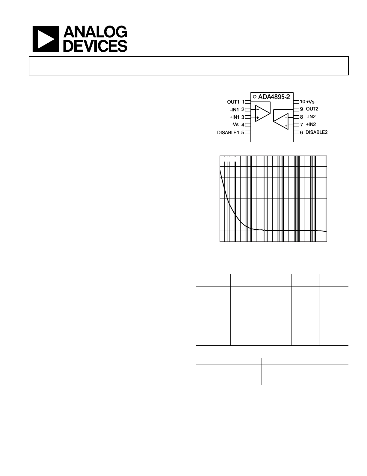
FUNCTIONAL BLOCK DIAGRAM
Figure 1. 10-Lead MSOP (ADA4895-2)
8
VS = ±5V
7
6
5
4
3
VOLTAGE NOISE (nV/√Hz)
2
1
0
1 10 100 1k 10k 100k 1M 5M
FREQUENCY (Hz)
Figure 2. Voltage Noise vs. Frequency
Table 1. Other Low Noise Amplifiers
(nV/√Hz)
V
N
Part Number
AD797 0.9 0.9 8 10 to 30
AD8021 5 2.1 490 5 to 24
AD8099 7 0.95 510 5 to 12
AD8045 6 3 1000 3.3 to 12
ADA4897-1 1 1 230 3 to 10
ADA4896-2 1 1 230 3 to 10
ADA4899-1 1.4 1 600 5 to 12
ADA4898-1/
ADA4898-2
@ 1 kHz
0.9 0.9 65 10 to 32
VN (nV/√Hz)
@ 100 kHz
BW (MHz)
Table 2. Complementary ADCs
Part Number Bits Speed (MSPS) Power (mW)
AD7944 14 2.5 15.5
AD7985 16 2.5 15.5
AD7986 18 2 15
09447-102
Supply
Voltage (V)
Rev. PrB
Information furnished by Analog Devices is believed to be accurate and reliable. However, no
responsibility is assumed by Analog Devices for its use, nor for any infringements of patents or other
rights of third parties that may result from its use. Specifications subject to change without notice. No
license is granted by implication or otherwise under any patent or patent rights of Analog Devices.
Trademarks and registered trademarks are the property of their respective owners.
One Technology Way, P.O. Box 9106, Norwood, MA 02062-9106, U.S.A.
Tel: 781.329.4700 www.analog.com
Fax: 781.461.3113 ©2011 Analog Devices, Inc. All rights reserved.

ADA4895-2 Preliminary Data Sheet
TABLE OF CONTENTS
Features .............................................................................................. 1
Applications ....................................................................................... 1
General Description ......................................................................... 1
Functional Block Diagram .............................................................. 1
Revision History ............................................................................... 2
Specifications ..................................................................................... 3
±5 V Supply ....................................................................................3
+5 V Supply ....................................................................................5
+3 V Supply ....................................................................................7
Pin Configurations and Function Descriptions ............................9
Typical Performance Characteristics ........................................... 10
Outline Dimensions ....................................................................... 12
Rev. PrB | Page 2 of 12

Preliminary Data Sheet ADA4895-2
SPECIFICATIONS
±5 V SUPPLY
TA = 25°C, G = +10, RL = 1 kΩ to ground, unless otherwise noted.
Table 3.
Parameter Conditions Min Typ Max Unit
DYNAMIC PERFORMANCE
–3 dB Bandwidth G = +10, V
G = +10, V
G = +20, V
Bandwidth for 0.1 dB Flatness G = +10, V
Slew Rate G = +10, V
Settling Time to 0.1% G = +10, V
Settling Time to 0.01% G = +10, V
NOISE/HARMONIC PERFORMANCE
Harmonic Distortion (dBc) SFDR fC = 100 kHz, V
f
f
f
= 1 MHz, V
C
= 2 MHz, V
C
= 5 MHz, V
C
Input Voltage Noise f = 10 Hz 2.4 nV/√Hz
f = 100 kHz 1 nV/√Hz
Input Current Noise f = 10 Hz 24 pA/√Hz
f = 100 kHz 2.94 pA/√Hz
0.1 Hz to 10 Hz Noise G = +101, RF = 1 kΩ, RG = 10 Ω 99 nV p-p
DC PERFORMANCE
Input Offset Voltage −500 −28 +500 μV
Input Offset Voltage Drift 0.2 μV/°C
Input Bias Current
−17 −11 −4 μA
Input Bias Current Drift 3 nA/°C
Input Bias Offset Current −0.6 −0.02 +0.6 μA
Open-Loop Gain V
= −4 V to +4 V 100 110 dB
OUT
INPUT CHARACTERISTICS
Input Resistance Common mode/differential 10 M/10 k Ω
Input Capacitance Common mode/differential 3/11 pF
Input Common-Mode Voltage Range −4.9 to +4.1 V
Common-Mode Rejection VCM = −2 V to +2 V −92 −120 dB
OUTPUT CHARACTERISTICS
Output Overdrive Recovery Time VIN = ±5 V, G = +2 81 ns
+Output Voltage Swing RL = 1 kΩ 4.85 4.96 V
−Output Voltage Swing RL = 1 kΩ −4.85 −4.97 V
+Output Voltage Swing RL = 100 Ω 4.5 4.73 V
−Output Voltage Swing RL = 100 Ω −4.5 −4.84 V
Output Current 45 dBc SFDR 80 mA
Short-Circuit Current Sinking/sourcing 135 mA
Capacitive Load Drive 30% overshoot, G = +2 39 pF
POWER SUPPLY
Operating Range 3 to 10 V
Quiescent Current per Amplifier 2.8 3 3.2 mA
DISABLE
Positive Power Supply Rejection +VS = 4 V to 6 V, −VS = −5 V −96 −125 dB
Negative Power Supply Rejection +VS = 5 V, −VS = −4 V to −6 V −96 −121 dB
= 0.2 V p-p 233 MHz
OUT
= 2 V p-p 140 MHz
OUT
= 0.2 V p-p TBD MHz
OUT
= 2 V p-p, RL = 100 Ω 10 MHz
OUT
= 6 V step 500 V/μs
OUT
= 2 V step TBD ns
OUT
= 2 V step TBD ns
OUT
= 2 V p-p −88 dBc
OUT
= 2 V p-p −68 dBc
OUT
= 2 V p-p −63 dBc
OUT
= 2 V p-p −55 dBc
OUT
= −5 V
0.25 mA
Rev. PrB | Page 3 of 12

ADA4895-2 Preliminary Data Sheet
Parameter Conditions Min Typ Max Unit
DISABLE PIN
DISABLE Voltage
Disabled <+VS – 2 V
Input Current
Enabled
Disabled
Switching Speed
Enabled 0.25 μs
Disabled 12 μs
Enabled >+V
DISABLE
DISABLE
= +5 V
= −5 V
−2.5 μA
−80 μA
− 0.5 V
S
Rev. PrB | Page 4 of 12

Preliminary Data Sheet ADA4895-2
+5 V SUPPLY
TA = 25°C, G = +10, RL = 1 kΩ to midsupply, unless otherwise noted.
Table 4.
Parameter Conditions Min Typ Max Unit
DYNAMIC PERFORMANCE
−3 dB Bandwidth G = +10, V
G = +10, V
G = +20, V
Bandwidth for 0.1 dB Flatness G = +10, V
Slew Rate G = +10, V
Settling Time to 0.1% G = +10, V
Settling Time to 0.01% G = +10, V
NOISE/HARMONIC PERFORMANCE
Harmonic Distortion (dBc) SFDR fC = 100 kHz, V
f
f
f
= 1 MHz, V
C
= 2 MHz, V
C
= 5 MHz, V
C
Input Voltage Noise f = 10 Hz 2.4 nV/√Hz
f = 100 kHz 1 nV/√Hz
Input Current Noise f = 10 Hz 24 pA/√Hz
f = 100 kHz 2.94 pA/√Hz
0.1 Hz to 10 Hz Noise G = +101, RF = 1 kΩ, RG = 10 Ω 99 nV p-p
DC PERFORMANCE
Input Offset Voltage −500 −30 +500 μV
Input Offset Voltage Drift 0.2 μV/°C
Input Bias Current −17 −11 −4 μA
Input Bias Current Drift 3 nA/°C
Input Bias Offset Current −0.6 −0.02 +0.6 μA
Open-Loop Gain V
= 0.5 V to 4.5 V 97 110 dB
OUT
INPUT CHARACTERISTICS
Input Resistance Common mode/differential 10 M/10 k Ω
Input Capacitance Common mode/differential 3/11 pF
Input Common-Mode Voltage Range 0.1 to 4.1 V
Common-Mode Rejection VCM = +1 V to +4 V −91 −118 dB
OUTPUT CHARACTERISTICS
Overdrive Recovery Time VIN = 0 V to 5 V, G = +2 96 ns
+Output Voltage Swing RL = 1 kΩ 4.85 4.98 V
−Output Voltage Swing RL = 1 kΩ 0.15 0.014 V
+Output Voltage Swing RL = 100 Ω 4.8 4.88 V
−Output Voltage Swing RL = 100 Ω 0.2 0.08
Output Current 45 dBc SFDR 70 mA
Short-Circuit Current Sinking/sourcing 125 mA
Capacitive Load Drive 30% overshoot, G = +2 39 pF
POWER SUPPLY
Operating Range 3 to 10 V
Quiescent Current per Amplifier 2.7 2.9 3.1 mA
DISABLE
Positive Power Supply Rejection +VS = 4.5 V to 5.5 V, −VS = 0 V −96 −123 dB
Negative Power Supply Rejection +VS = 5 V, −VS = −0.5 V to +0.5 V −96 −121 dB
= 0.2 V p-p 203 MHz
OUT
= 2 V p-p 127 MHz
OUT
= 0.2 V p-p TBD MHz
OUT
= 2 V p-p, RL = 100 Ω 9.8 MHz
OUT
= 3 V step 451 V/μs
OUT
= 2 V step TBD ns
OUT
= 2 V step TBD ns
OUT
= 2 V p-p −86 dBc
OUT
= 2 V p-p −66 dBc
OUT
= 2 V p-p −60 dBc
OUT
= 2 V p-p −53 dBc
OUT
= 0 V
0.18
Rev. PrB | Page 5 of 12

ADA4895-2 Preliminary Data Sheet
Parameter Conditions Min Typ Max Unit
DISABLE PIN
DISABLE Voltage
Disabled <+VS − 2 V
Input Current
Enabled
Disabled
Switching Speed
Enabled 0.25 μs
Disabled 12 μs
Enabled >+V
DISABLE
DISABLE
= +5 V
= 0 V
−2.5 μA
−50 μA
− 0.5 V
S
Rev. PrB | Page 6 of 12

Preliminary Data Sheet ADA4895-2
+3 V SUPPLY
TA = 25°C, G = +1, RL = 1 kΩ to midsupply, unless otherwise noted.
Table 5.
Parameter Conditions Min Typ Max Unit
DYNAMIC PERFORMANCE
−3 dB Bandwidth G = +10, V
G = +10, V
G = +20, V
Bandwidth for 0.1 dB Flatness G = +10, V
Slew Rate G = +10, V
Settling Time to 0.1% G = +10, V
Settling Time to 0.01% G = +10, V
NOISE/HARMONIC PERFORMANCE
Harmonic Distortion (dBc) SFDR fC = 100 kHz, V
f
f
f
= 1 MHz, V
C
= 2 MHz, V
C
= 5 MHz, V
C
Input Voltage Noise f = 10 Hz 2.3 nV/√Hz
f = 100 kHz 1 nV/√Hz
Input Current Noise f = 10 Hz 24 pA/√Hz
f = 100 kHz 2.94 pA/√Hz
0.1 Hz to 10 Hz Noise G = +101, RF = 1 kΩ, RG = 10 Ω 99 nV p-p
DC PERFORMANCE
Input Offset Voltage −500 −30 +500 uV
Input Offset Voltage Drift 0.2 μV/°C
Input Bias Current −17 −11 −4 μA
Input Bias Current Drift 3 nA/°C
Input Bias Offset Current −0.6 −0.02 +0.6 μA
Open-Loop Gain V
= 0.5 V to 2.5 V 95 108 dB
OUT
INPUT CHARACTERISTICS
Input Resistance Common mode/differential 10 M/10 k Ω
Input Capacitance Common mode/differential 3/11 pF
Input Common-Mode Voltage Range 0.1 to 2.1 V
Common-Mode Rejection VCM = +1.1 V to +1.9 V −90 −124 dB
OUTPUT CHARACTERISTICS
Overdrive Recovery Time VIN = 0 V to +3 V, G = +2 83 ns
+Output Voltage Swing RL = 1 kΩ 2.85 2.97 V
−Output Voltage Swing RL = 1 kΩ 0.15 0.01 V
+Output Voltage Swing RL = 100 Ω 2.8 2.92 V
−Output Voltage Swing RL = 100 Ω 0.2 0.05 V
Output Current 45 dBc SFDR 60 mA
Short-Circuit Current Sinking/sourcing 120 mA
Capacitive Load Drive 30% overshoot, G = +2 39 pF
POWER SUPPLY
Operating Range 3 to 10 V
Quiescent Current per Amplifier 2.6 2.8 3 mA
DISABLE
Positive Power Supply Rejection +VS = 2.7 V to 3.7 V, −VS = 0 V −96 −121 dB
Negative Power Supply Rejection +VS = 3 V, −VS = −0.3 V to 0.7 V −96 −120 dB
= 0.2 V p-p 192 MHz
OUT
= 1 V p-p 124 MHz
OUT
= 0.2 V p-p 9.2 MHz
OUT
= 2 V p-p, RL = 100 Ω TBD MHz
OUT
= 1 V step 450 V/μs
OUT
= 2 V step TBD ns
OUT
= 2 V step TBD ns
OUT
= 2 V p-p, G = +2 −85 dBc
OUT
= 1 V p-p, G = −1 −65 dBc
OUT
= 1 V p-p, G = −1 −59 dBc
OUT
= 1 V p-p, G = −1 −52 dBc
OUT
= 0 V
0.15
Rev. PrB | Page 7 of 12

ADA4895-2 Preliminary Data Sheet
Parameter Conditions Min Typ Max Unit
DISABLE PIN
DISABLE Voltage
Disabled <−VS + 2 V
Input Current
Enabled
Disabled
Switching Speed
Enabled 0.25 μs
Disabled 12 μs
Enabled >+V
DISABLE
DISABLE
= +3 V
= 0 V
−2.5 μA
−40 μA
−0.5 V
S
Rev. PrB | Page 8 of 12
Preliminary Data Sheet ADA4895-2
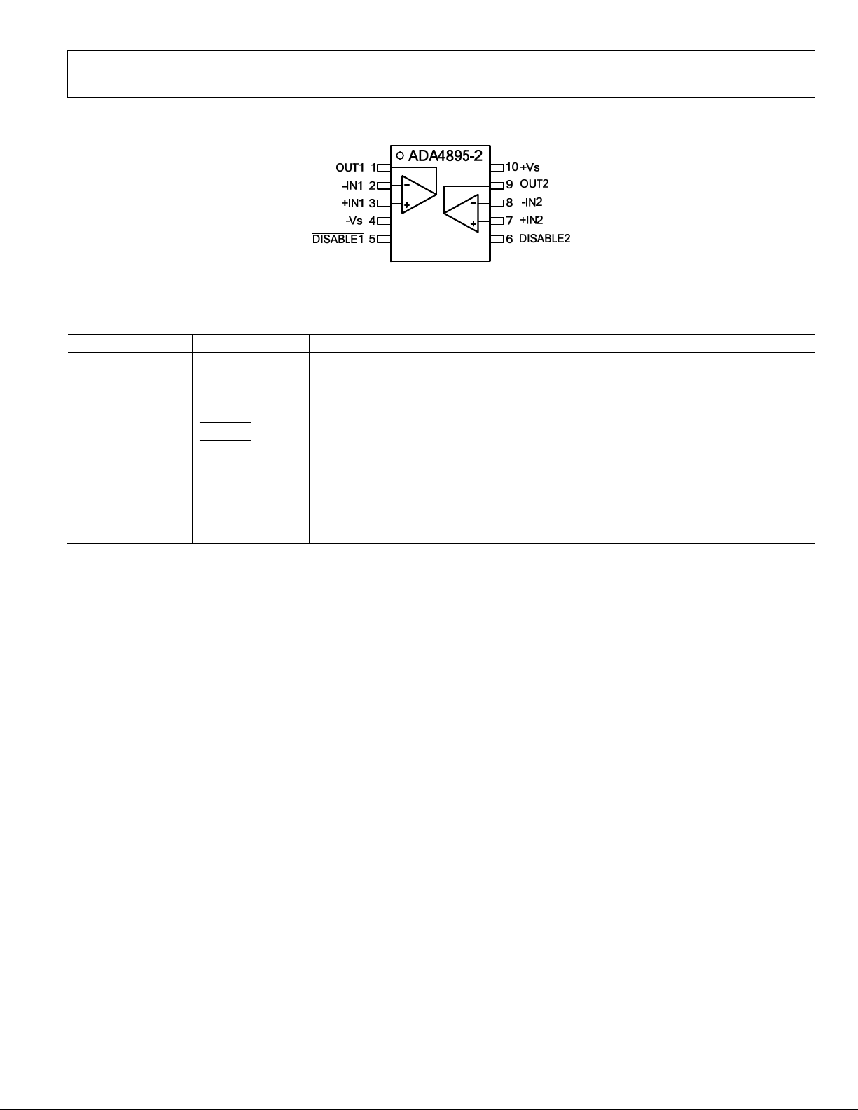
PIN CONFIGURATIONS AND FUNCTION DESCRIPTIONS
Figure 3. 10-Lead ADA4895-2 MSOP (10)
Table 6. ADA4895-2 Pin Function Descriptions
Pin No. Mnemonic Description
1 OUT1 Output 1.
2 −IN1 Inverting Input 1.
3 +IN1 Noninverting Input 1.
4 −VS Negative Supply.
5
6
7 +IN2 Noninverting Input 2.
8 −IN2 Inverting Input 2.
9 OUT2 Output 2.
10 +VS Positive Supply.
EPAD Exposed Pad. The exposed pad can be connected to GND or left floating.
DISABLE1
DISABLE2
Disable1.
Disable2.
Rev. PrB | Page 9 of 12

ADA4895-2 Preliminary Data Sheet
√
TYPICAL PERFORMANCE CHARACTERISTICS
RL = 1 kΩ,unless otherwise noted.When G = +10, RF = 249 Ω.
Figure 4. Small Signal Frequency Response vs. Supply Voltage
Figure 5. Harmonic Distortion vs. Frequency for various supplies
8
VS = ±5V
7
6
5
4
Figure 7. Large Signal Frequency Response vs. Supply Voltage
Figure 8. 0.1 dB Bandwidth at Selected RF Value
100
Hz)
10
V
= ±5V
S
3
VOLTAGE NOISE (nV/√Hz)
2
1
0
1
100
10
FREQUENC Y (Hz)
10k 100k 1M
1k
5M
09447-027
Figure 6. Voltage Noise vs. Frequency
CURRENT NOISE (pA/
1
1 10 100
1k 10k 100k 1M 5M
FREQUENCY (Hz)
Figure 9. Current Noise vs. Frequency
09447-060
Rev. PrB | Page 10 of 12

Preliminary Data Sheet ADA4895-2
0
–100
POWER SUP PLY REJECT ION (dB)
–110
–120
–130
–10
–20
–30
–40
–50
–60
–70
–80
–90
VS = +5V
ΔV
= 2V p-p
S
G = +1
–PSRR
+PSRR
1M 10M
FREQUENCY ( Hz)
Figure 12. PSRR vs. Frequency
100M100k10k1k
09447-030
4
OUT
V
IN
3
2
1
0
–1
–2
INPUT AND OUTPUT VOLTAGE (V)
–3
–4
V
TIME = 100n s/DIV
= +5V
V
S
G = +1
09447-049
Figure 10. Input Overdrive Recovery
Figure 11.Small Signal Transient Response for Various Supplies
Figure 13. Large Signal Transient Response for Various Gains
Rev. PrB | Page 11 of 12

OUTLINE DIMENSIONS
3.10
3.00
2.90
10
6
3.10
3.00
2.90
PIN 1
IDENTIFIER
0.95
0.85
0.75
0.15
0.05
COPLANARITY
1
0.50 BSC
0.10
COMPLIANT TO JEDEC STANDARDS MO-187-BA
5.15
4.90
4.65
5
1.10 MAX
0.30
0.15
6°
0°
Figure 14. 10-Lead Mini Small Outline Package [MSOP]
(RM-10)
Dimensions shown in millimeters
15° MAX
0.23
0.13
0.70
0.55
0.40
teehSataD yranimilerP 2-5984ADA
091709-A
©2011 Analog Devices, Inc. All rights reserved. Trademarks and
registered trademarks are the property of their respective owners.
PR10186-0-9/11(PrB)
Rev. PrB | Page 12 of 12
 Loading...