


High Speed, G = +2,
www.BDTIC.com/ADI
FEATURES
Ideal for RGB/HD/SD video
Supports 1080i/720p resolution
High speed
−3 dB bandwidth: 300 MHz
Slew rate: 750 V/μs
Settling time: 9 ns ( 0.5%)
0.1 dB flatness: 65 MHz
Differential gain: 0.02%
Differential phase: 0.03°
Wide supply range: 5 V to 12 V
Low power: 5.3 mA/amp
Low voltage offset (RTO): 3.5 mV (typ)
High output current: 25 mA
Also configurable for gains of +1, −1
Power-down
APPLICATIONS
Consumer video
Professional video
Filter buffers
GENERAL DESCRIPTION
Low Cost, Triple Op Amp
ADA4862-3
PIN CONFIGURATION
POWER DOWN 1
POWER DOWN 2
POWER DOWN 3
+V
+IN 1
–IN 1
V
OUT
1
2
3
ADA4862-3
4
S
5
550Ω 550Ω
6
7
1
550Ω 550Ω
Figure 1. 14-Lead SOIC (R-14)
550Ω
550Ω
14
V
2
OUT
13
–IN 2
12
+IN 2
11
–V
S
10
+IN 3
9
–IN 3
8
V
3
OUT
05600-001
The ADA4862-3 (triple) is a low cost, high speed, internally
fixed, G = +2 op amp, which provides excellent overall
performance for high definition and RGB video applications.
The 300 MHz, G = +2, −3 dB bandwidth, and 750 V/μs slew
rate make this amplifier well suited for many high speed
applications. The ADA4862-3 can also be configured to
operate in gains of G = +1 and G = −1.
With its combination of low price, excellent differential gain
(0.02%), dif
ferential phase (0.03°), and 0.1 dB flatness out to
65 MHz, this amplifier is ideal for both consumer and
professional video applications.
The ADA4862-3 is designed to operate on supply voltages as
lo
w as +5 V and up to ±5 V using only 5.3 mA/amp of supply
current. To further reduce power consumption, each amplifier
is equipped with a power-down feature that lowers the supply
current to 200 μA/amp. The ADA4862-3 also consumes less
board area because feedback and gain set resistors are on-chip.
Having the resistors on chip simplifies layout and minimizes the
required board space.
Rev. A
Information furnished by Analog Devices is believed to be accurate and reliable. However, no
responsibility is assumed by Anal og Devices for its use, nor for any infringements of patents or ot her
rights of third parties that may result from its use. Specifications subject to change without notice. No
license is granted by implication or otherwise under any patent or patent rights of Analog Devices.
Trademarks and registered trademarks are the property of their respective owners.
The ADA4862-3 is available in a 14-lead SOIC package and is
desig
ned to work in the extended temperature range of −40°C
to +105°C.
6.1
6.0
5.9
G = +2
5.8
R
= 150Ω
L
C
= 4pF
L
5.7
V
= 2V p-p
OUT
5.6
5.5
5.4
CLOSED-LOOP GAIN (dB)
5.3
5.2
5.1
0.1 1000
1 10 100
FREQUENCY (MHz)
VS = ±5V
Figure 2. Large Signal 0.1 dB Bandwidth for Various Supplies
One Technology Way, P.O. Box 9106, Norwood, MA 02062-9106, U.S.A.
Tel: 781.329.4700 www.analog.com
Fax: 781.461.3113 © 2005 Analog Devices, Inc. All rights reserved.
VS = +5V
05600-022

ADA4862-3
www.BDTIC.com/ADI
TABLE OF CONTENTS
Features .............................................................................................. 1
Applications..................................................................................... 11
Applications....................................................................................... 1
Pin Configuration............................................................................. 1
General Description......................................................................... 1
Revision History ............................................................................... 2
Specifications..................................................................................... 3
Absolute Maximum Ratings............................................................ 5
Thermal Resistance ...................................................................... 5
ESD Caution.................................................................................. 5
Typical Performance Characteristics ............................................. 6
REVISION HISTORY
8/05—Rev. 0 to Rev. A
Changes to Ordering Guide.......................................................... 15
7/05—Revision 0: Initial Version
Using the ADA4862-3 in Gains = +1, −1................................ 11
Video Line Driver....................................................................... 13
Single-Supply Operation ........................................................... 13
Power Down ................................................................................ 13
Layout Considerations............................................................... 14
Power Supply Bypassing ............................................................ 14
Outline Dimensions ....................................................................... 15
Ordering Guide .......................................................................... 15
Rev. A | Page 2 of 16
ADA4862-3
www.BDTIC.com/ADI
SPECIFICATIONS
VS = +5 V (@TA = 25oC, G = +2, RL = 150 Ω, unless otherwise noted).
Table 1.
Parameter Conditions Min Typ Max Unit
DYNAMIC PERFORMANCE
–3 dB Bandwidth VO = 0.2 V p-p 300 MHz
V
G = +1 VO = 0.2 V p-p 620 MHz
Bandwidth for 0.1 dB Flatness VO = 2 V p-p 65 MHz
+Slew Rate (Rising Edge) VO = 2 V p-p 750 V/μs
−Slew Rate (Falling Edge) VO = 2 V p-p 600 V/μs
Settling Time to 0.5% VO = 2 V step 9 ns
DISTORTION/NOISE PERFORMANCE
Harmonic Distortion HD2 fC = 1 MHz, VO = 2 V p-p −81 dBc
Harmonic Distortion HD3 fC = 1 MHz, VO = 2 V p-p −88 dBc
Harmonic Distortion HD2 fC = 5 MHz, VO = 2 V p-p −68 dBc
Harmonic Distortion HD3 fC = 5 MHz, VO = 2 V p-p −76 dBc
Voltage Noise (RTO) f = 100 kHz 10.6 nV/√Hz
Current Noise (RTI) f = 100 kHz, +IN 1.4 pA/√Hz
Differential Gain 0.02 %
Differential Phase 0.03 Degrees
Crosstalk
DC PERFORMANCE
Offset Voltage (RTO) Referred to output (RTO) −25 +3.5 +25 mV
+Input Bias Current −2.5 −0.6 +1 μA
Gain Accuracy 1.9 2 2.1 V/V
INPUT CHARACTERISTICS
Input Resistance +IN 13 MΩ
Input Capacitance +IN 2 pF
Input Common-Mode Voltage Range G = +1 1 to 4 V
POWER DOWN PIN
Input Voltage Enabled 0.6 V
Power down 1.8 V
Bias Current Enabled −3 μA
Power down 115 μA
Turn-On Time 3.5 μs
Turn-Off Time 200 ns
OUTPUT CHARACTERISTICS
Output Overdrive Recovery Time (Rise/Fall) VIN = +2.25 V to −0.25 V 85/50 ns
Output Voltage Swing RL = 150 Ω 1.2 to 3.8 V
Output Voltage Swing RL = 1 kΩ 1 to 4 V
Short-Circuit Current Sinking or sourcing 65 mA
POWER SUPPLY
Operating Range 5 12 V
Total Quiescent Current Enabled 14 16 18 mA
Quiescent Current /Amplifier Power down = +V
Power Supply Rejection Ratio (RTO) dB
+PSR +VS = 2 V to 3 V, −VS = −2.5 V −52 −55 dB
−PSR
= 2 V p-p 200 MHz
O
Amplifier 1 driven, Amplifier 2 output
ed, f = 1 MHz
measur
S
= 2.5 V, −VS = −2 V to −3 V
+V
S
Power Down pin = −V
S
−75 dB
0.2 0.33 mA
−49 −52 dB
Rev. A | Page 3 of 16
ADA4862-3
www.BDTIC.com/ADI
VS = ±5 V (@TA = +25oC, G = +2, RL = 150 Ω, unless otherwise noted).
Table 2.
Parameter Conditions Min Typ Max Unit
DYNAMIC PERFORMANCE
–3 dB Bandwidth VO = 0.2 V p-p 310 MHz
V
G = +1 VO = 0.2 V p-p 720 MHz
Bandwidth for 0.1 dB Flatness VO = 2 V p-p 54 MHz
+Slew Rate (Rising Edge) VO = 2 V p-p 1050 V/μs
−Slew Rate (Falling Edge) VO = 2 V p-p 830 V/μs
Settling Time to 0.5% VO = 2 V step 9 ns
DISTORTION/NOISE PERFORMANCE
Harmonic Distortion HD2 fC = 1 MHz, VO = 2 V p-p −87 dBc
Harmonic Distortion HD3 fC = 1 MHz, VO = 2 V p-p −100 dBc
Harmonic Distortion HD2 fC = 5 MHz, VO = 2 V p-p −74 dBc
Harmonic Distortion HD3 fC = 5 MHz, VO = 2 V p-p −90 dBc
Voltage Noise (RTO) f = 100 kHz 10.6 nV/√Hz
Current Noise (RTI) f = 100 kHz, +IN 1.4 pA/√Hz
Differential Gain 0.01 %
Differential Phase 0.02 Degrees
Crosstalk
DC PERFORMANCE
Offset Voltage (RTO) −25 +2 +25 mV
+Input Bias Current
Gain Accuracy 1.9 2 2.1 V/V
INPUT CHARACTERISTICS
Input Resistance +IN 14 MΩ
Input Capacitance +IN 2 pF
Input Common-Mode Voltage Range G = +1 −3.7 to +3.8 V
POWER DOWN PIN
Input Voltage Enabled −4.4 V
Power down −3.2 V
Bias Current Enabled
Power down
Turn-On Time 3.5 μs
Turn-Off Time 200 ns
OUTPUT CHARACTERISTICS
Output Overdrive Recovery Time (Rise/Fall) VIN = ±3.0 V 85/40 ns
Output Voltage Swing RL = 150 Ω −3.5 to +3.5 V
Output Voltage Swing RL = 1 kΩ −3.9 to +3.9 V
Short-Circuit Current Sinking or sourcing 115 mA
POWER SUPPLY
Operating Range 5 12 V
Total Quiescent Current Enabled 14.5 17.9 20.5 mA
Quiescent Current/Amplifier Power down = +V
Power Supply Rejection Ratio (RTO) dB
+PSR +VS = 4 V to 6 V, −VS = −5 V −54 −57 dB
−PSR
= 2 V p-p 260 MHz
O
Amplifier 1 driven, Amplifier 2 output
ed, f = 1 MHz
measur
−2.5 −0.6 +1 μA
S
= 5 V, −VS = −4 V to −6 V,
+V
S
Power Down pin = −V
S
−75 dB
−3 μA
250 μA
0.3 0.5 mA
+50.5 −54 dB
Rev. A | Page 4 of 16
ADA4862-3
www.BDTIC.com/ADI
ABSOLUTE MAXIMUM RATINGS
Table 3.
Parameter Rating
Supply Voltage 12.6 V
Power Dissipation See Figure 3
Common-Mode Input Voltage
±V
S
Storage Temperature −65°C to +125°C
Operating Temperature Range −40°C to +105°C
Lead Temperature JEDEC J-STD-20
Junction Temperature 150°C
The power dissipated in the package (P
) is the sum of the
D
quiescent power dissipation and the power dissipated in the die due
to the amplifier’s drive at the output. The quiescent power is the
voltage between the supply pins (V
= Quiescent Power + (Tota l D ri v e P o we r − Load Power)
P
D
⎛
()
D
S
IVP
SS
×+×=
⎜
2
⎝
) × the quiescent current (IS).
S
2
OUT
R
V
⎞
OUT
–
⎟
R
L
L
⎠
VV
Stresses above those listed under Absolute Maximum Ratings
may cause permanent damage to the device. This is a stress
rating only; functional operation of the device at these or any
other conditions above those indicated in the operational
section of this specification is not implied. Exposure to absolute
maximum rating conditions for extended periods may affect
device reliability.
THERMAL RESISTANCE
θJA is specified for the worst-case conditions, that is, θJA is
specified for device soldered in circuit board for surface-mount
packages.
Table 4. Thermal Resistance
Package Type θ
JA
14-lead SOIC 90 °C/W
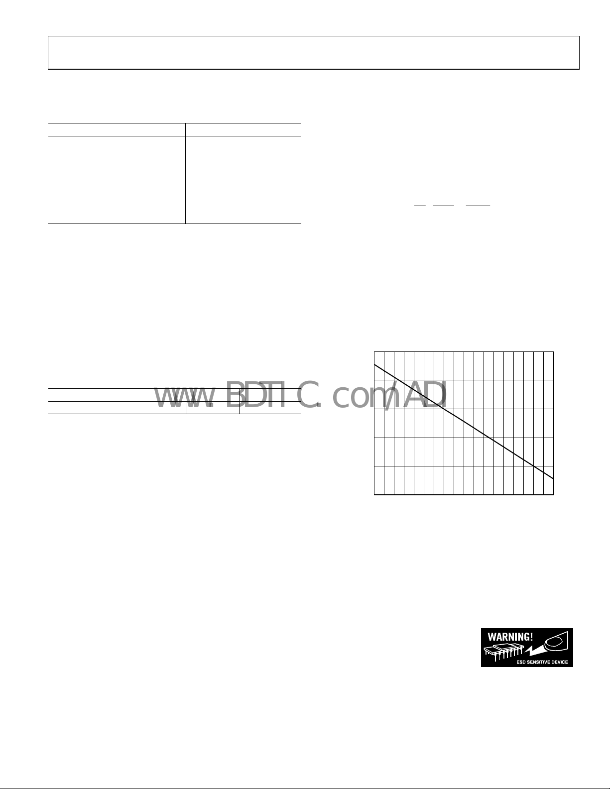
Maximum Power Dissipation
The maximum safe power dissipation for the ADA4862-3 is
limited by the associated rise in junction temperature (T
the die. At approximately 150°C, which is the glass transition
temperature, the plastic changes its properties. Even
temporarily exceeding this temperature limit may change the
stresses that the package exerts on the die, permanently shifting
the parametric performance of the amplifiers. Exceeding a
junction temperature of 150°C for an extended period can
result in changes in silicon devices, potentially causing
degradation or loss of functionality.
Unit
) on
J
RMS output voltages should be considered.
Airflow increases heat dissipation, effectively reducing θ
.
JA
In addition, more metal directly in contact with the package
leads and through holes under the device reduces θ
.
JA
Figure 3 shows the maximum safe power dissipation in the
ackage vs. the ambient temperature for the 14-lead SOIC
p
(90°C/W) on a JEDEC standard 4-layer board. θ
values are
JA
approximations.
2.5
2.0
1.5
1.0
0.5
MAXIMUM POWER DISSIPATION (W)
0
–55 125–45 –35 –25 –15 –5 5 15 25 35 45 55 65 75 85 95 105 115
Figure 3. Maximum Power Dissipation vs. Temperature for a 4-Layer Board
AMBIENT TEMPERATURE (°C)
05600-036
ESD CAUTION
ESD (electrostatic discharge) sensitive device. Electrostatic charges as high as 4000 V readily accumulate on
the human body and test equipment and can discharge without detection. Although this product features
proprietary ESD protection circuitry, permanent damage may occur on devices subjected to high energy
electrostatic discharges. Therefore, proper ESD precautions are recommended to avoid performance
degradation or loss of functionality.
Rev. A | Page 5 of 16

ADA4862-3
www.BDTIC.com/ADI
TYPICAL PERFORMANCE CHARACTERISTICS
8
G = +2
R
= 150Ω
L
7
C
= 4pF
L
V
= 0.2V p-p
OUT
6
5
4
3
CLOSED-LOOP GAIN (dB)
2
1
0
0.1 1000
1 10 100
FREQUENCY (MHz)
VS = ±5V
VS = +5V
05600-004
200 2.7
VS = +5V
100 2.6
V
= ±5V
S
= 5V
0 2.5
S
±V
OUTPUT VOLTAGE (mV)
–100 2.4
–200 2.3
G = +2
R
= 150Ω
L
= 4pF
C
L
V
= 0.2V p-p
OUT
TIME = 5ns/DIV
= 0V
S
= 5V, –V
S
+V
OUTPUT VOLTAGE (V)
05600-028
Figure 4. Small Signal Frequency Response for Various Supplies
8
G = +2
R
= 150Ω
L
7
C
= 4pF
L
V
= 2V p-p
OUT
6
5
4
3
CLOSED-LOOP GAIN (dB)
2
1
0
0.1 1000
1 10 100
FREQUENCY (MHz)
VS = +5V
VS = ±5V
Figure 5. Large Signal Frequency Response for Various Supplies
6.1
6.0
5.9
G = +2
5.8
R
= 150Ω
L
C
= 4pF
L
5.7
V
= 2V p-p
OUT
5.6
5.5
5.4
CLOSED-LOOP GAIN (dB)
5.3
5.2
5.1
0.1 1000
1 10 100
FREQUENCY (MHz)
VS = ±5V
VS = +5V
Figure 6. Large Signal 0.1 dB Bandwidth for Various Supplies
05600-012
05600-022
Figure 7. Small Signal Transient Response for Various Supplies
200
150
100
50
0
–50
OUTPUT VOLTAGE (V)
–100
–150
–200
CL= 9pF
CL= 4pF
CL= 6pF
G = +2
R
= 150Ω
L
C
= 4pF
L
V
= 0.2V p-p
OUT
= ±5V
V
S
TIME = 5ns/DIV
Figure 8. Small Signal Transient Response for Various Capacitor Loads
2.7
CL= 9pF
CL= 6pF
2.6
CL= 4pF
2.5
OUTPUT VOLTAGE (V)
2.4
2.3
G = +2
R
= 150Ω
L
= 0.2V p-p
V
OUT
= 5V
V
S
TIME = 5ns/DIV
Figure 9. Small Signal Transient Response for Various Capacitor Loads
05600-016
05600-014
Rev. A | Page 6 of 16

ADA4862-3
www.BDTIC.com/ADI
1.5 4.0
1.0 3.5
VS = +5V
0.5 3.0
= 5V
0 2.5
S
±V
–0.5 2.0
OUTPUT VOLTAGE (V)
–1.0 1.5
–1.5 1.0
VS = ±5V
G = +2
R
= 150Ω
L
= 4pF
C
L
= 2V p-p
V
OUT
TIME = 5ns/DIV
Figure 10. Large Signal Transient Response for Various Supplies
= 0V
S
= 5V, –V
S
+V
OUTPUT VOLTAGE (V)
05600-010
6
5
4
3
2
1
0
–1
–2
–3
OUTPUT AND INPUT VOLTAGE (V)
–4
–5
–6
0 1000
100 200 300 400 500 600 700 800 900
INPUT VOLTAGE × 2
V
OUT
TIME (ns)
Figure 13. Input Overdrive Recovery
VS = ±5V
G = +2
= 150Ω
R
L
= 4pF
C
L
f = 1MHz
05600-042
1.5
1.0
0.5
0
–0.5
OUTPUT VOLTAGE (V)
–1.0
–1.5
CL = 9pF
CL = 6pF
CL = 4pF
G = +2
= 150Ω
R
L
= 4pF
C
L
= 2V p-p
V
OUT
V
= ±5V
S
TIME = 5ns/DIV
Figure 11. Large Signal Transient Response for Various Capacitor Loads
4.0
3.5
3.0
2.5
CL = 9pF
CL = 6pF
CL = 4pF
05600-018
5.5
5.0
4.5
4.0
3.5
3.0
2.5
2.0
1.5
1.0
OUTPUT AND INPUT VOLTAGE (V)
0.5
0
–0.5
0 1000
100 200 300 400 500 600 700 800 900
Figure 14. Output Ove
INPUT VOLTAGE × 2
V
OUT
TIME (ns)
rdrive Recovery
VS = 5V
G = +2
= 150Ω
R
L
= 4pF
C
L
f = 1MHz
05600-041
2.0
OUTPUT VOLTAGE (V)
1.5
1.0
G = +2
= 150Ω
R
L
= 4pF
C
L
V
= 2V p-p
OUT
= 5V
V
S
TIME = 5ns/DIV
05600-019
Figure 12. Large Signal Transient Response for Various Capacitor Loads
Rev. A | Page 7 of 16

ADA4862-3
www.BDTIC.com/ADI
1.5
1.0
V
OUT
0.5
(V)
IN
0
AND V
OUT
V
–0.5
–1.0
–1.5
050
V
IN
5 1015202530354045
TIME (ns)
VS = ±5V, +5V
G = +2
V
OUT
R
L
C
L
V
OUT
EXPANDED
= 2V p-p
=150Ω
= 4pF
20
15
10
5
0
–5
–10
–15
–20
EXPANDED (mV)
OUT
V
05600-043
1.5
1.0
0.5
(V)
IN
0
AND V
OUT
V
–0.5
–1.0
–1.5
5 1015202530354045
050
Figure 15. Settling Time Falling Edge
V
OUT
V
IN
V
OUT
EXPANDED
TIME (ns)
V
S
G = +2
V
OUT
R
L
C
L
Figure 18. Settling Time Rising Edge
= ±5V, +5V
= 2V p-p
= 150Ω
= 4pF
20
15
10
5
0
–5
–10
–15
–20
EXPANDED (mV)
OUT
V
05600-046
1600
G = +2
V
= ±5V
S
1400
R
= 150Ω
L
C
= 4pF
L
1200
1000
800
600
SLEW RATE (V/μs)
400
200
0
0 5.0
0.5 1.0 1.5 2.0 2.5 3.0 3.5 4.0 4.5
OUTPUT VOLTAGE STEP (V p-p)
POSITIVE SLEW RATE
NEGATIVE SLEW RATE
Figure 16. Slew Rate vs. Output Voltage
100
10
G = +2
R
= 150Ω
L
= 4pF
C
L
V
OUT
= ±5V
V
S
= +5V
V
S
= 2V p-p
05600-005
800
G = +2
V
= 5V
S
700
R
= 150Ω
L
C
= 4pF
L
600
s)
μ
500
400
300
SLEW RATE (V/
200
100
0
0.5 1.0 1.5 2.0 2.5
0 3.0
OUTPUT VOLTAGE STEP (V p-p)
POSITIVE SLEW RATE
NEGATIVE SLEW RATE
Figure 19. Slew Rate vs. Output Voltage
0
G = +2
R
= 150Ω
L
C
= 4pF
L
–20
V
= 2V p-p
OUT
V
= ±5V
S
V
= +5V
S
–40
–60
05600-006
VOLTAGE NOISE (nV/ Hz)
1
10
100 1k 10k 100k 1M 10M
FREQUENCY (Hz)
100M
05600-037
Figure 17. Voltage Noise vs. Frequency Referred to Output (RTO)
Rev. A | Page 8 of 16
CROSSTALK (dB)
–80
–100
–120
0.1 1000
1 10 100
FREQUENCY (MHz)
Figure 20. Large Signal Crosstalk
05600-023

ADA4862-3
www.BDTIC.com/ADI
19
18
0
VS = ±5V
–10
–20
17
16
TOTAL SUPPLY CURRENT (mA)
15
4
567891011
Figure 21. Total Supply Current vs. V
20
19
18
17
16
15
14
TOTAL SUPPLY CURRENT (mA)
13
12
–40 125
–25–105 203550658095110
SUPPLY VOLTAGE (V)
SUPPLY
VS = ±5V
VS = +5V
TEMPERATURE (°C)
12
Figure 22. Total Supply Current at Various Supplies vs. Temperature
05600-026
05600-021
–30
–40
–50
POWER SUPPLY REJECTION (dB)
–60
–70
0.01
0.1 1 10 100
Figure 23. Power Supply R
0
VS = ±2.5V
–10
–20
–30
–40
POWER SUPPLY REJECTION (dB)
–50
–60
0.01 1000
0.1 1 10 100
Figure 24. Power Supply R
–PSR
+PSR
FREQUENCY (MHz)
ejection vs. Frequency
–PSR
+PSR
FREQUENCY (MHz)
ejection vs. Frequency
05600-051
1000
05600-052
Rev. A | Page 9 of 16

ADA4862-3
www.BDTIC.com/ADI
–50
G = +2
= 150Ω
R
L
= 4pF
C
L
–60
HD2
= ±5V
V
S
–70
–80
–90
DISTORTION (dBc)
–100
–110
04
123
fO = 10MHz
OUTPUT VOLTAGE (V p-p)
fO = 20MHz
fO = 5MHz
fO = 2MHz
fO = 1MHz
05600-049
Figure 25. HD2 vs. Frequency vs. Output Voltage
–50
G = +2
= 150Ω
R
L
–60
= 4pF
C
L
HD3
= ±5V
V
–70
S
–80
–90
–100
DISTORTION (dBc)
–110
–120
–130
04
fO = 20MHz
fO = 1MHz
123
OUTPUT VOLTAGE (V p-p)
f
fO = 2MHz
= 10MHz
O
fO = 5MHz
05600-054
Figure 27. HD3 vs. Frequency vs. Output Voltage
–50
G = +2
= 150Ω
R
L
= 4pF
C
L
–60
HD2
= 5V
V
S
–70
–80
–90
DISTORTION (dBc)
–100
–110
0 2.5
0.5 1.0 1.5 2.0
fO = 20MHz
fO = 10MHz
fO = 5MHz
fO = 2MHz
fO = 1MHz
OUTPUT VOLTAGE (V p-p)
Figure 26. HD2 vs. Frequency vs. Output Voltage
05600-050
–50
–60
–70
–80
–90
–100
DISTORTION (dBc)
–110
–120
–130
0 2.5
fO = 20MHz
f
= 10MHz
O
fO = 2MHz
fO = 1MHz
0.5 1.0 1.5 2.0
OUTPUT VOLTAGE (V p-p)
Figure 28. HD3 vs. Frequency vs. Output Voltage
fO = 5MHz
G = +2
= 150Ω
R
L
= 4pF
C
L
HD3
= +5V
V
S
05600-048
Rev. A | Page 10 of 16

ADA4862-3
V
www.BDTIC.com/ADI
APPLICATIONS
USING THE ADA4862-3 IN GAINS = +1, −1
The ADA4862-3 was designed to offer outstanding video
performance, simplify applications, and minimize board area.
The ADA4862-3 is a triple amplifier with on-chip feedback and
ga
in set resistors. The gain is fixed internally at G = +2. The
inclusion of the on-chip resistors not only simplifies the design
of the application but also eliminates six surface-mount
resistors, saving valuable board space and lowers assembly
+V
–V
+V
S
Figure 29.
S
10μF
0.01μF
0.01μF
10μF
S
10μF
0.01μF
0.01μF
V
OUT
05600-029
V
OUT
costs. A typical schematic is shown in
V
IN
R
T
GAIN OF +2
Figure 29. Noninverting Configuration (G = +2)
While the ADA4862-3 has a fixed gain of G = +2, it can be used
in other gain configurations, such as G = −1 and G = +1, which
are discussed next.
Unity-Gain Operation (Option 1)
There are two options for obtaining unity gain (G = +1). The
first is shown in Figure 30. In this configuration, the –IN input
in is left floating (feedback is provided via the internal 550 Ω),
p
and the input is applied to the noninverting input. The noise
gain for this configuration is 1. Frequency performance and
transient response are shown in Figure 31 through Figure 33.
IN
R
T
4
G = +1
= 150Ω
R
L
3
= 4pF
C
L
= 200mV p-p
V
OUT
2
1
0
–1
CLOSED-LOOP GAIN (dB)
–2
–3
–4
0.1 1000
1 10 100
FREQUENCY (MHz)
VS = +5V
VS = ±5V
Figure 31. Small Signal Unity Gain
3
G = +1
= 150Ω
R
2
L
= 4pF
C
L
= 2V p-p
V
OUT
1
0
–1
–2
–3
CLOSED-LOOP GAIN (dB)
–4
–5
–6
0.1 1000
1 10 100
FREQUENCY (MHz)
VS = +5V
VS = ±5V
Figure 32. Large Signal Gain +1
2.0
1.5
1.0
0.5
0
–0.5
OUTPUT VOLTAGE (V)
–1.0
–1.5
–2.0
CL= 9pF
CL= 6pF
CL= 4pF
G = +1
= 150Ω
R
L
V
= 2V p-p
OUT
= ±5V
V
S
TIME = 5ns/DIV
Figure 33. Large Signal Transient Response for Various Capacitor Loads
05600-053
05600-002
05600-020
10μF
–V
S
GAIN OF +1
05600-032
Figure 30. Unity Gain of Option 1
Rev. A | Page 11 of 16

ADA4862-3
www.BDTIC.com/ADI
Option 2
Another option exists for running the ADA4862-3 as a unitygain amplifier. In this configuration, the noise gain is 2, see
Figure 34. The frequency response and transient response for
nfiguration closely match the gain of +2 plots because the
this co
noise gains are equal. This method does have twice the noise
gain of Option 1; however, in applications that do not require
low noise, Option 2 offers less peaking and ringing. By tying the
inputs together, the net gain of the amplifier becomes 1.
Equation 1 shows the transfer characteristic for the schematic
shown in
shown i
which simplifies to V
Figure 34. Frequency and transient response are
n Figure 35 and Figure 36.
⎛
−
R
⎜
=
VV
i
O
⎜
R
G
⎝
V
IN
1
0
G = +1
= 150Ω
R
–1
L
–2
–3
GAIN (dB)
–4
–5
–6
–7
0.1
Figure 35. Frequency Response of Option 2
⎛
⎞
F
⎜
⎟
+
V
i
⎜
⎟
⎝
⎠
= Vi.
O
R
T
+
RR
F
R
G
R
G
GAIN OF +1
⎞
G
⎟
(1)
⎟
⎠
+V
S
10μF
0.01μF
R
F
0.01μF
10μF
–V
S
Figure 34. Unity Gain of Option 2
1 10 100
FREQUENCY (MHz)
V
OUT
05600-030
05600-027
1000
200
G = +1
V
= ±5V
S
150
R
= 150Ω
L
TIME = 2ns/DIV
100
50
0
–50
OUTPUT VOLTAGE (mV)
–100
–150
–200
Figure 36. Small Signals Transient Response of Option 2
+V
S
10μF
0.01μF
V
IN
R
T
0.01μF
10μF
–V
S
GAIN OF –1
V
OUT
05600-031
Figure 37. Inverting Configuration (G = −1)
2.0
1.5
1.0
0.5
0
–0.5
OUTPUT VOLTAGE (V)
–1.0
–1.5
–2.0
CL= 9pF
CL= 6pF
CL= 4pF
G = –1
= 150Ω
R
L
= 2V p-p
V
OUT
= ±5V
V
S
TIME = 5ns/DIV
Figure 38. Large Signal Transient Response for Various Capacitor Loads
05600-039
05600-017
Rev. A | Page 12 of 16

ADA4862-3
V
V
V
www.BDTIC.com/ADI
VIDEO LINE DRIVER
The ADA4862-3 was designed to excel in video driver
applications. Figure 39 shows a typical schematic for a video
iver operating on a bipolar supplies.
dr
+V
S
10μF
0.1μF
–
ADA4862-3
+
75Ω
CABLE
IN
75Ω
0.1μF
10μF
–V
S
Figure 39. Video Driver Schematic
In applications that require two video loads be driven
simultaneously, the ADA4862-3 can deliver. Figure 40 shows
e ADA4862-3 configured with dual video loads. Figure 41
th
ws the dual video load performance.
sho
+V
S
10μF
0.1μF
7
–
2
8
6
+
0.1μF
10μF
–V
S
VS = +5V
75Ω
CABLE
IN
75Ω
Figure 40. Video Driver Schematic for Two Video Loads
8
G = +2
R
= 75Ω
L
7
C
= 4pF
L
V
OUT
6
5
4
3
CLOSED-LOOP GAIN (dB)
2
1
= 2V p-p
75Ω
75Ω
75Ω
75Ω
CABLE
75Ω
CABLE
75Ω
CABLE
VS = ±5V
75Ω
75Ω
75Ω
V
OUT
V
V
05600-033
OUT
OUT
1
2
05600-034
SINGLE-SUPPLY OPERATION
The ADA4862-3 can also operate in single-supply applications.
Figure 42 shows the schematic for a single 5 V supply video
iver. Resistors R2 and R4 establish the midsupply reference.
dr
Capacitor C2 is the bypass capacitor for the midsupply
reference. Capacitor C1 is the input coupling capacitor, and C6
is the output coupling capacitor. Capacitor C5 prevents constant
current from being drawn through the internal gain set resistor.
Resistor R3 sets the circuits ac input impedance.
For more information on single-supply operation of op amps,
www.analog.com/library/analogDialogue/a
see
rchives/35-
02/avoiding/.
C2
1μF
R4
R2
50kΩ
50kΩ
+5V
R3
1kΩ
IN
R1
50Ω
C1
22μF
22μF
C5
Figure 42. Single-Supply Vide
+5V
C3
2.2μF
C4
0.01μF
–V
S
o Driver Schematic
C6
220μF
R5
75Ω
ADA4862-3
R6
75Ω
V
OUT
05600-035
POWER DOWN
The ADA4862-3 is equipped with an independent Power Down
pin for each amplifier allowing the user to reduce the supply
current when an amplifier is inactive. The voltage applied to the
pin is the logic reference, making single-supply applications
−V
S
useful with conventional logic levels. In a typical 5 V singlesupply application, the −V
The amplifiers are powered down when applied logic levels are
greater than −V
+ 1 V. The amplifiers are enabled whenever the
S
disable pins are left either floating (disconnected) or the
applied logic levels are lower than 1 V above −V
pin is connected to analog ground.
S
.
S
1
0
0.1
1 10 100
FREQUENCY (MHz)
Figure 41. Large Signal Frequency Response for Various Supplies, R
1000
= 75 Ω
L
05600-008
Rev. A | Page 13 of 16

ADA4862-3
www.BDTIC.com/ADI
LAYOUT CONSIDERATIONS
As is the case with all high speed applications, careful attention
to printed circuit board layout details prevents associated board
parasitics from becoming problematic. Proper RF design
technique is mandatory. The PCB should have a ground plane
covering all unused portions of the component side of the
board to provide a low impedance return path. Removing the
ground plane on all layers from the area near the input and
output pins reduces stray capacitance. Termination resistors and
loads should be located as close as possible to their respective
inputs and outputs. Input and output traces should be kept as
far apart as possible to minimize coupling (crosstalk) though
the board. Adherence to microstrip or stripline design
techniques for long signal traces (greater than about 1 inch) is
recommended.
POWER SUPPLY BYPASSING
Careful attention must be paid to bypassing the power supply
pins of the ADA4862-3. High quality capacitors with low
equivalent series resistance (ESR), such as multilayer ceramic
capacitors (MLCCs), should be used to minimize supply voltage
ripple and power dissipation. A large, usually tantalum, 10 μF to
47 μF capacitor located in proximity to the ADA4862-3 is
required to provide good decoupling for lower frequency
signals. In addition, 0.1 μF MLCC decoupling capacitors should
be located as close to each of the power supply pins as is
physically possible, no more than 1/8 inch away. The ground
returns should terminate immediately into the ground plane.
Locating the bypass capacitor return close to the load return
minimizes ground loops and improves performance.
Rev. A | Page 14 of 16

ADA4862-3
www.BDTIC.com/ADI
OUTLINE DIMENSIONS
8.75 (0.3445)
8.55 (0.3366)
4.00 (0.1575)
3.80 (0.1496)
0.25 (0.0098)
0.10 (0.0039)
COPLANARITY
0.10
CONTROLLING DIMENSIONS ARE IN MILLIMETERS; INCH DIMENSIONS
(IN PARENTHESES) ARE ROUNDED-OFF MILLIMETER EQUIVALENTS FOR
REFERENCE ONLY AND ARE NOT APPROPRIATE FOR USE IN DESIGN
14
1
1.27 (0.0500)
BSC
0.51 (0.0201)
0.31 (0.0122)
COMPLIANT TO JEDEC STANDARDS MS-012-AB
Figure 43. 14-Lead Standard Small Outline Package [SOIC_N]
Dimensions shown in millimeters and (inches)
8
6.20 (0.2441)
7
5.80 (0.2283)
1.75 (0.0689)
1.35 (0.0531)
SEATING
PLANE
Nar
row Body
(R-14)
0.25 (0.0098)
0.17 (0.0067)
0.50 (0.0197)
0.25 (0.0098)
8°
0°
1.27 (0.0500)
0.40 (0.0157)
× 45°
ORDERING GUIDE
Model Temperature Range Package Description Ordering Quantity Package Option
ADA4862-3YRZ
ADA4862-3YRZ-RL
ADA4862-3YRZ-RL7
1
Z = Pb-free part.
1
1
1
–40°C to +105°C 14-Lead SOIC_N 1 R-14
–40°C to +105°C 14-Lead SOIC_N 2,500 R-14
–40°C to +105°C 14-Lead SOIC_N 1,000 R-14
Rev. A | Page 15 of 16

ADA4862-3
www.BDTIC.com/ADI
NOTES
© 2005 Analog Devices, Inc. All rights reserved. Trademarks and
registered trademarks are the property of their respective owners.
D05600–0–8/05(A)
Rev. A | Page 16 of 16
 Loading...