

High Speed, Low Cost,
www.BDTIC.com/ADI
FEATURES
High speed
730 MHz, −3 dB bandwidth
625 V/μs slew rate
13 ns settling time to 0.5%
Wide supply range: 5 V to 12 V
Low power: 6 mA/amplifier
0.1 dB flatness: 100 MHz
Differential gain: 0.01%
Differential phase: 0.02°
Low voltage offset: 100 μV (typical)
High output current: 25 mA
Power down
APPLICATIONS
Consumer video
Professional video
Broadband video
ADC buffers
Active filters
GENERAL DESCRIPTION
The ADA4861-3 is a low cost, high speed, current feedback,
triple op amp that provides excellent overall performance. The
730 MHz, −3 dB bandwidth, and 625 V/μs slew rate make this
amplifier well suited for many high speed applications. With its
combination of low price, excellent differential gain (0.01%),
differential phase (0.02°), and 0.1 dB flatness out to 100 MHz,
this amplifier is ideal for both consumer and professional video
applications.
The ADA4861-3 is designed to operate on supply voltages as
lo
w as +5 V and up to ±5 V using only 6 mA/amplifier of supply
current. To further reduce power consumption, each amplifier
is equipped with a power-down feature that lowers the supply
current to 0.3 mA/amplifier when not being used.
The ADA4861-3 is available in a 14-lead SOIC_N package and
ned to work over the extended temperature range of
is desig
−40°C to +105°C.
Triple Op Amp
ADA4861-3
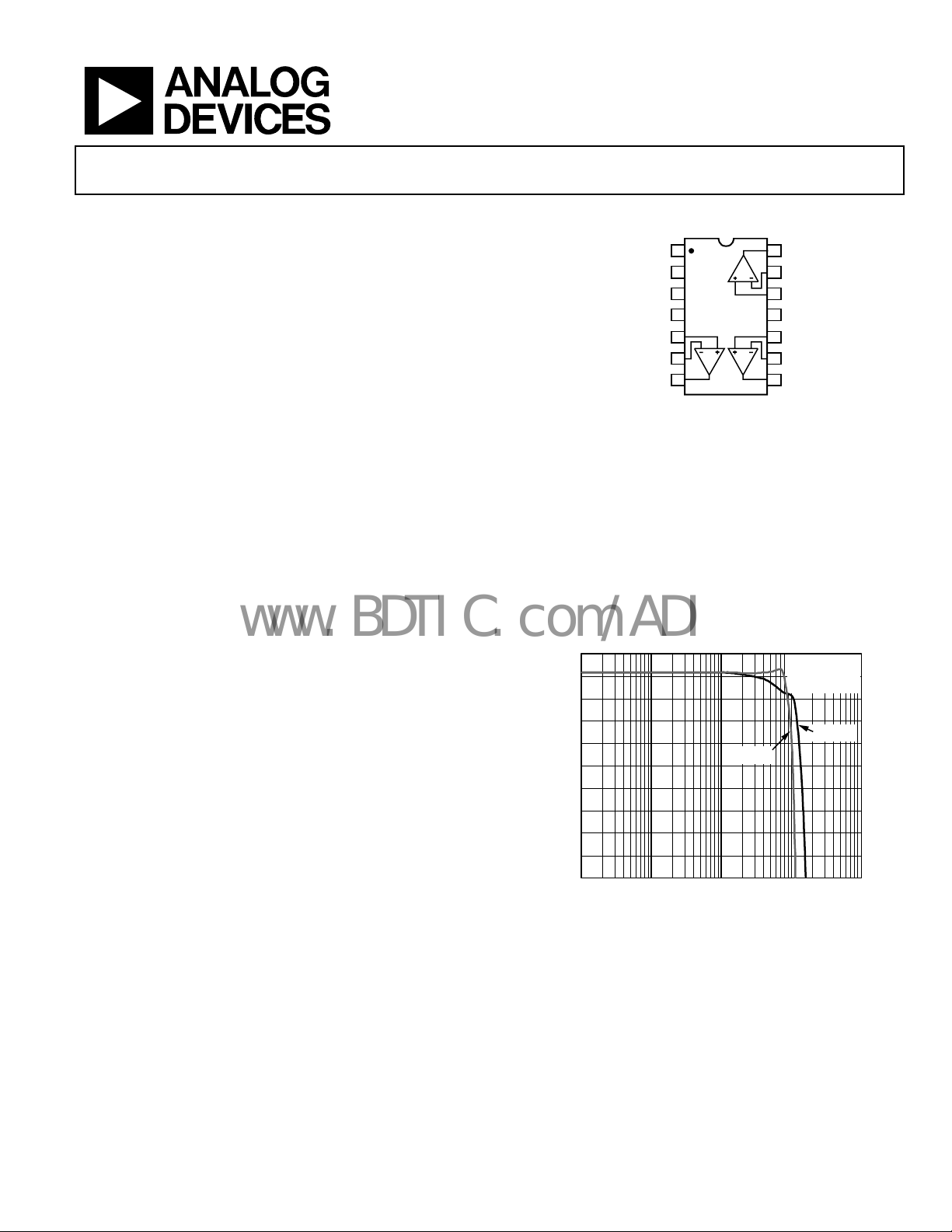
PIN CONFIGURATION
+V
+IN 1
–IN 1
OUT 1
1
2
3
4
S
5
6
7
ADA4861-3
POWER DOW N 1
POWER DOW N 2
POWER DOW N 3
Figure 1.
6.1
6.0
5.9
5.8
5.7
5.6
5.5
5.4
CLOSED-LOOP GAIN (dB)
5.3
5.2
5.1
0.1 1 10 100 1000
FREQUENCY (MHz)
Figure 2. Large Signal 0.1 dB Flatness
VS = +5V
14
13
12
11
10
9
8
OUT 2
–IN 2
+IN 2
–V
S
+IN 3
–IN 3
OUT 3
G = +2
V
OUT
R
= RG = 301Ω
F
05708-001
= 2V p-p
= ±5V
V
S
05708-011
Rev. A
Information furnished by Analog Devices is believed to be accurate and reliable. However, no
responsibility is assumed by Anal og Devices for its use, nor for any infringements of patents or ot her
rights of third parties that may result from its use. Specifications subject to change without notice. No
license is granted by implication or otherwise under any patent or patent rights of Analog Devices.
Trademarks and registered trademarks are the property of their respective owners.
One Technology Way, P.O. Box 9106, Norwood, MA 02062-9106, U.S.A.
Tel: 781.329.4700 www.analog.com
Fax: 781.461.3113 ©2006 Analog Devices, Inc. All rights reserved.

ADA4861-3
www.BDTIC.com/ADI
TABLE OF CONTENTS
Features.............................................................................................. 1
Gain Configurations .................................................................. 13
Applications....................................................................................... 1
Pin Configuration............................................................................. 1
General Description ......................................................................... 1
Revision History ............................................................................... 2
Specifications..................................................................................... 3
Absolute Maximum Ratings............................................................ 5
Thermal Resistance ...................................................................... 5
ESD Caution.................................................................................. 5
Typical Performance Characteristics ............................................. 6
Applications..................................................................................... 13
REVISION HISTORY
3/06—Rev 0 to Rev. A
Changes to 20 MHz Active Low-Pass Filter Section.................. 13
Changes to Figure 48 and Figure 49............................................. 13
10/05—Revision 0: Initial Version
20 MHz Active Low-Pass Filter................................................ 13
RGB Video Driver...................................................................... 14
Driving Two Video Loads ......................................................... 14
POWER-DOWN Pins ............................................................... 14
Single-Supply Operation........................................................... 15
Power Supply Bypassing............................................................ 15
Layout .......................................................................................... 15
Outline Dimensions....................................................................... 16
Ordering Guide .......................................................................... 16
Rev. A | Page 2 of 16
ADA4861-3
www.BDTIC.com/ADI
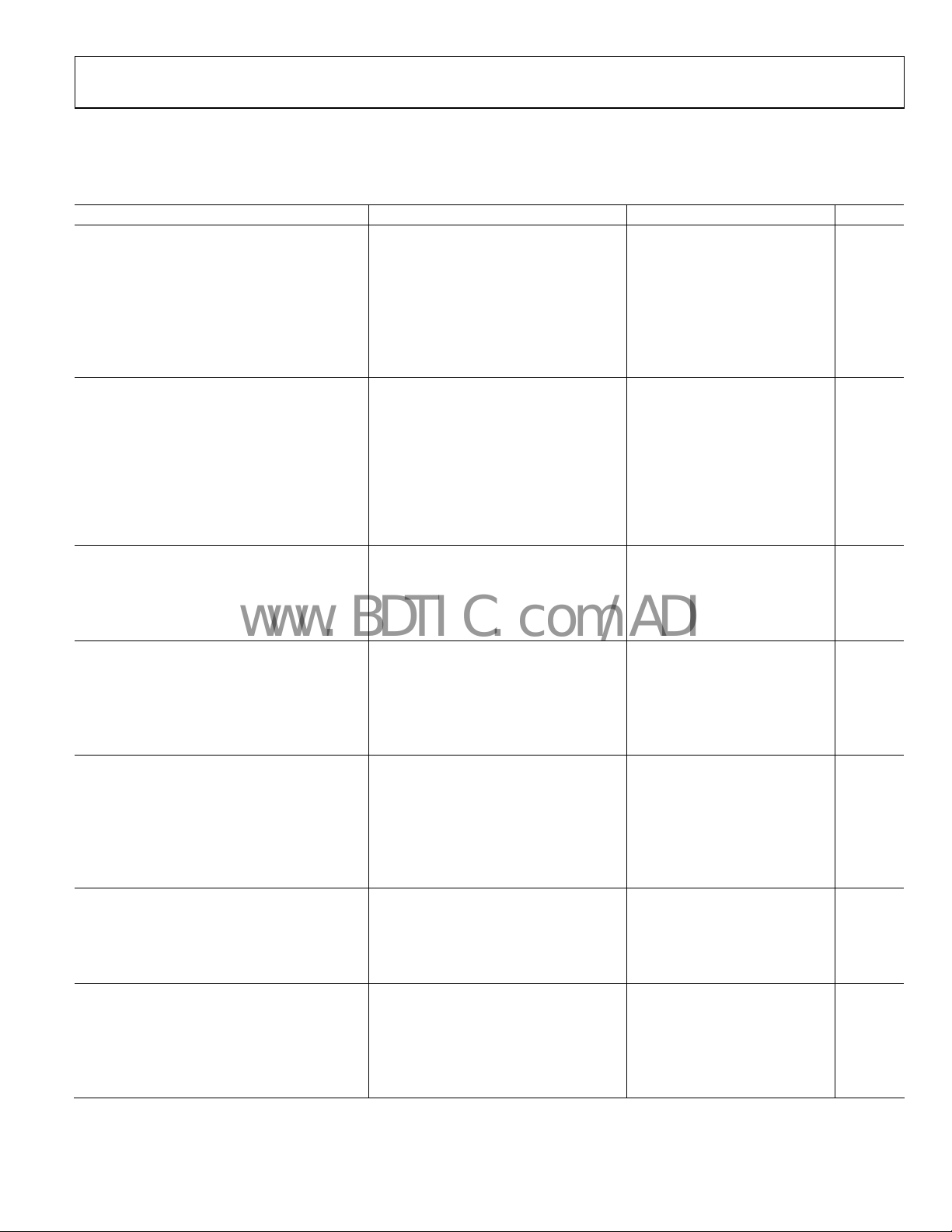
SPECIFICATIONS
VS = +5 V (@ TA = 25°C, G = +2, RL = 150 Ω, CL = 4 pF, unless otherwise noted); for G = +2, RF = RG = 301 Ω; and for G = +1, RF = 499 Ω.
Table 1.
Parameter Conditions Min Typ Max Unit
DYNAMIC PERFORMANCE
–3 dB Bandwidth VO = 0.2 V p-p 350 MHz
V
G = +1, VO = 0.2 V p-p 560 MHz
Bandwidth for 0.1 dB Flatness VO = 2 V p-p 85 MHz
+Slew Rate (Rising Edge) VO = 2 V p-p 590 V/μs
−Slew Rate (Falling Edge) VO = 2 V p-p 480 V/μs
Settling Time to 0.5% (Rise/Fall) VO = 2 V step 12/13 ns
NOISE/DISTORTION PERFORMANCE
Harmonic Distortion HD2/HD3 fC = 1 MHz, VO = 2 V p-p −81/−89 dBc
Harmonic Distortion HD2/HD3 fC = 5 MHz, VO = 2 V p-p −69/−76 dBc
Input Voltage Noise f = 100 kHz 3.8 nV/√Hz
Input Current Noise f = 100 kHz, +IN/−IN 1.7/5.5 pA/√Hz
Differential Gain 0.02 %
Differential Phase 0.03 Degrees
All-Hostile Crosstalk
DC PERFORMANCE
Input Offset Voltage −13 −0.9 +13 mV
+Input Bias Current
−Input Bias Current −8 +2.3 +13 μA
Open-Loop Transresistance 400 620 kΩ
INPUT CHARACTERISTICS
Input Resistance +IN 14 MΩ
−IN 85 Ω
Input Capacitance +IN 1.5 pF
Input Common-Mode Voltage Range G = +1 1.2 to 3.8 V
Common-Mode Rejection Ratio VCM = 2 V to 3 V −54 −56.5 dB
POWER-DOWN PINS
Input Voltage Enabled 0.6 V
Power down 1.8 V
Bias Current Enabled −3 μA
Power down 115 μA
Turn-On Time 200 ns
Turn-Off Time 3.5 μs
OUTPUT CHARACTERISTICS
Output Overdrive Recovery Time (Rise/Fall) VIN = +2.25 V to −0.25 V 55/100 ns
Output Voltage Swing RL = 150 Ω 1.2 to 3.8 1.1 to 3.9 V
R
Short-Circuit Current Sinking and sourcing 65 mA
POWER SUPPLY
Operating Range 5 12 V
Total Quiescent Current Enabled 12.5 16.1 18.5 mA
Quiescent Current/Amplifier POWER DOWN pins = +VS 0.2 0.33 mA
Power Supply Rejection Ratio
+PSR +VS = 4 V to 6 V, −VS = 0 V −60 −64 dB
= 2 V p-p 145 MHz
O
Amplifier 1 and Amplifier 2 driven,
Amplifier 3 output measur
−2 −0.8 +1 μA
= 1 kΩ 0.9 to 4.1 0.85 to 4.15 V
L
ed, f = 1 MHz
−65 dB
Rev. A | Page 3 of 16
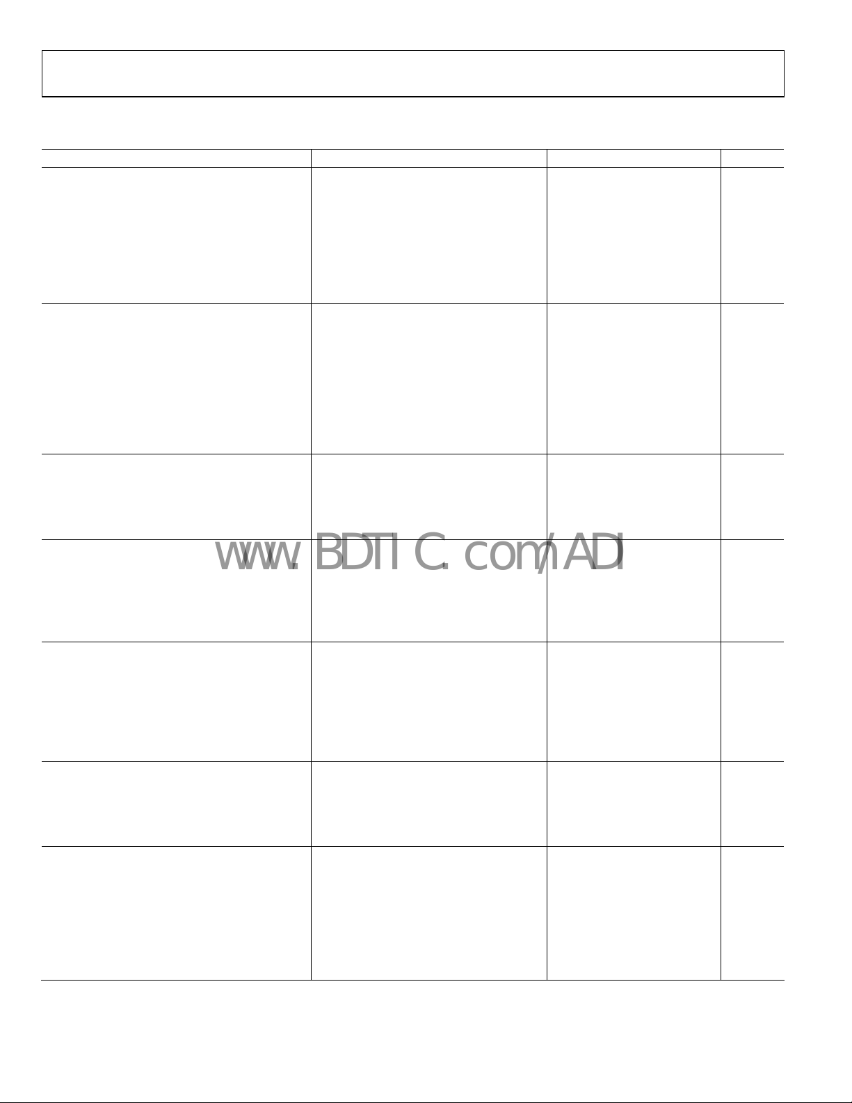
ADA4861-3
www.BDTIC.com/ADI
VS = ±5 V (@ TA = 25°C, G = +2, RL = 150 Ω, CL = 4 pF, unless otherwise noted); for G = +2, RF = RG = 301 Ω; and for G = +1, RF = 499 Ω.
Table 2.
Parameter Conditions Min Typ Max Unit
DYNAMIC PERFORMANCE
–3 dB Bandwidth VO = 0.2 V p-p 370 MHz
V
G = +1, VO = 0.2 V p-p 730 MHz
Bandwidth for 0.1 dB Flatness VO = 2 V p-p 100 MHz
+Slew Rate (Rising Edge) VO = 2 V p-p 910 V/μs
−Slew Rate (Falling Edge) VO = 2 V p-p 680 V/μs
Settling Time to 0.5% (Rise/Fall) VO = 2 V step 12/13 ns
NOISE/DISTORTION PERFORMANCE
Harmonic Distortion HD2/HD3 fC = 1 MHz, VO = 2 V p-p −85/−99 dBc
Harmonic Distortion HD2/HD3 fC = 5 MHz, VO = 2 V p-p −73/−86 dBc
Input Voltage Noise f = 100 kHz 3.8 nV/√Hz
Input Current Noise f = 100 kHz, +IN/−IN 1.7/5.5 pA/√Hz
Differential Gain 0.01 %
Differential Phase 0.02 Degrees
All-Hostile Crosstalk
DC PERFORMANCE
Input Offset Voltage −13 −0.1 +13 mV
+Input Bias Current
−Input Bias Current −8 +2.9 +13 μA
Open-Loop Transresistance 500 720 kΩ
INPUT CHARACTERISTICS
Input Resistance +IN 15 MΩ
−IN 90 Ω
Input Capacitance +IN 1.5 pF
Input Common-Mode Voltage Range G = +1 −3.7 to +3.7 V
Common-Mode Rejection Ratio VCM = ±2 V −55 −58 dB
POWER-DOWN PINS
Input Voltage Enabled −4.4 V
Power down −3.2 V
Bias Current Enabled −3 μA
Power down 250 μA
Turn-On Time 200 ns
Turn-Off Time 3.5 μs
OUTPUT CHARACTERISTICS
Output Overdrive Recovery Time (Rise/Fall) VIN = ±3.0 V 30/90 ns
Output Voltage Swing RL = 150 Ω ±2 −3.1 to +3.65 V
R
Short-Circuit Current Sinking and sourcing 100 mA
POWER SUPPLY
Operating Range 5 12 V
Total Quiescent Current Enabled 13.5 17.9 20.5 mA
Quiescent Current/Amplifier POWER DOWN pins = +VS 0.3 0.5 mA
Power Supply Rejection Ratio
+PSR +VS = 4 V to 6 V, −VS = −5 V −63 −66 dB
−PSR
= 2 V p-p 210 MHz
O
Amplifier 1 and Amplifier 2 driven,
Amplifier 3 output measur
−2 −0.7 +1 μA
= 1 kΩ ±3.9 ±4.05 V
L
= 5 V, −VS = −4 V to −6 V,
+V
S
POWER DOWN pins = −V
ed, f = 1 MHz
S
−65 dB
−59 −62 dB
Rev. A | Page 4 of 16
ADA4861-3
www.BDTIC.com/ADI
ABSOLUTE MAXIMUM RATINGS
Table 3.
Parameter Rating
Supply Voltage 12.6 V
Power Dissipation See Figure 3
Common-Mode Input Voltage −VS + 1 V to +VS − 1 V
Differential Input Voltage ±VS
Storage Temperature −65°C to +125°C
Operating Temperature Range −40°C to +105°C
Lead Temperature JEDEC J-STD-20
Junction Temperature 150°C
Stresses above those listed under Absolute Maximum Ratings
y cause permanent damage to the device. This is a stress
ma
rating only; functional operation of the device at these or any
other conditions above those indicated in the operational
section of this specification is not implied. Exposure to absolute
maximum rating conditions for extended periods may affect
device reliability.
THERMAL RESISTANCE
θJA is specified for the worst-case conditions, that is, θJA is
specified for device soldered in circuit board for surface-mount
packages.
Table 4. Thermal Resistance
Package Type θJA Unit
14-lead SOIC_N 90 °C/W
Maximum Power Dissipation
The maximum safe power dissipation for the ADA4861-3 is
limited by the associated rise in junction temperature (T
the die. At approximately 150°C, which is the glass transition
temperature, the plastic changes its properties. Even temporarily
exceeding this temperature limit can change the stresses that the
package exerts on the die, permanently shifting the parametric
performance of the amplifiers. Exceeding a junction temperature of
150°C for an extended period can result in changes in silicon
devices, potentially causing degradation or loss of functionality.
) on
J
The power dissipated in the package (P
quiescent power dissipation and the power dissipated in the die
due to the amplifiers’ drive at the output. The quiescent power
is the voltage between the supply pins (V
current (I
).
S
= Quiescent Power + (Total Drive Power − Load Power)
P
D
VV
⎛
S
()
D
IVP
SS
OUT
×+×=
⎜
2
R
⎝
L
RMS output voltages should be considered.
Airflow increases heat dissipation, effectively reducing θ
In addition, more metal directly in contact with the package
leads and through holes under the device reduces θ
Figure 3 shows the maximum safe power dissipation in the
ackage vs. the ambient temperature for the 14-lead SOIC_N
p
(90°C/W) on a JEDEC standard 4-layer board. θ
approximations.
2.5
2.0
1.5
1.0
0.5
MAXIMUM POW ER DISSIPAT ION (W)
0
–55 125–45–35–25–15–5 5 152535455565758595105115
AMBIENT TEMPERATURE (°C)
Figure 3. Maximum Power Dissipation vs. Temperature for a 4-Layer Board
) is the sum of the
D
) times the quiescent
S
2
V
⎞
OUT
–
⎟
R
L
⎠
.
JA
values are
JA
.
JA
05708-002
ESD CAUTION
ESD (electrostatic discharge) sensitive device. Electrostatic charges as high as 4000 V readily accumulate on
the human body and test equipment and can discharge without detection. Although this product features
proprietary ESD protection circuitry, permanent damage may occur on devices subjected to high energy
electrostatic discharges. Therefore, proper ESD precautions are recommended to avoid performance
degradation or loss of functionality.
Rev. A | Page 5 of 16

ADA4861-3
www.BDTIC.com/ADI
TYPICAL PERFORMANCE CHARACTERISTICS
RL = 150 Ω and CL = 4 pF, unless otherwise noted.
1
0
VS = ±5V
V
= 0.2V p-p
OUT
G = +1,
R
= 499Ω
F
1
0
VS = 5V
V
OUT
= 0.2V p- p
G = +1, RF = 499Ω
–1
–2
–3
–4
NORMALIZED GAIN (dB)
–5
–6
0.1 1 10 100 1000
G = +2, RF = RG = 301Ω
G = –1, R
= RG = 301Ω
F
= 200Ω, RG = 49.9Ω
G = +5, R
F
G = +10, R
= 200Ω, RG = 22.1Ω
F
FREQUENCY (MHz)
Figure 4. Small Signal Frequency Response for Various Gains
1
VS = ±5V
V
= 2V p-p
OUT
0
–1
–2
–3
–4
NORMALIZED GAIN (dB)
–5
–6
G = +5, RF = 200Ω, RG = 49.9Ω
G = +1, RF = 499Ω
G = +2, RF = RG = 301Ω
G = +10, RF = 200Ω, RG = 22.1Ω
0.1 1 10 100 1000
FREQUENCY (MHz)
G = –1, RF = RG = 301Ω
–1
–2
–3
–4
NORMALIZED GAIN (dB)
–5
05708-038
–6
0.1 1 10 100 1000
G = –1, R
G = +5, R
G = +10, R
= RG = 301Ω
G = +2, R
F
= RG = 301Ω
F
= 200Ω, RG = 49.9Ω
F
= 200Ω, RG = 22.1Ω
F
FREQUENCY (MHz)
Figure 7. Small Signal Frequency Response for Various Gains
1
VS = 5V
V
= 2V p-p
OUT
0
–1
–2
–3
–4
NORMALIZED GAIN (dB)
–5
05708-028
–6
1 1 10 100 1000
0.
G = +1, RF = 499Ω
G = +2, RF = RG = 301Ω
G = +10, RF = 200Ω, RG = 22.1Ω
G = +5, RF = 200Ω, RG = 49.9Ω
G = –1, RF = RG = 301Ω
FREQUENCY (MHz)
05708-037
05708-027
Figure 5. Large Signal Frequency Response for Various Gains
6.1
6.0
5.9
5.8
5.7
5.6
5.5
5.4
CLOSED-LOOP GAIN (dB)
5.3
5.2
5.1
0.1 1 10 100 1000
FREQUENCY (MHz)
VS = +5V
G = +2
V
= 2V p-p
OUT
R
= RG = 301Ω
F
V
S
= ±5V
05708-011
Figure 6. Large Signal 0.1 dB Flatness
Rev. A | Page 6 of 16
Figure 8. Large Signal Frequency Response for Various Gains
7
VS = ±5V
G = +2
6
5
= 2V p-p
V
V
OUT
OUT
= 4V p-p
4
3
2
CLOSED-LOOP GAIN (dB)
1
0
0.1 1 10 100 1000
FREQUENCY (MHz)
V
OUT
= 1V p-p
Figure 9. Large Signal Frequency Response for Various Output Levels
05708-029

ADA4861-3
–
–
–
–
www.BDTIC.com/ADI
7
= 301Ω
R
6
5
4
3
R
F
R
F
= 499Ω
= 604Ω
F
R
F
= 402Ω
7
= 301Ω
R
6
5
4
3
R
F
R
F
= 499Ω
= 604Ω
F
R
F
= 402Ω
2
CLOSED-LOOP GAIN (dB)
VS = ±5V
1
G = +2
R
= R
G
F
V
= 0.2V p- p
OUT
0
0.1 1 10 100 1000
FREQUENCY (MHz )
Figure 10. Small Signal Frequency Response vs. R
05708-012
F
2
CLOSED-LOOP GAIN (dB)
VS = ±5V
1
G = +2
R
= R
F
G
V
= 2V p-p
OUT
0
0.1 1 10 100 1000
Figure 13. Large Signal Frequency Response vs. R
40
VS = ±5V
G = +1
–50
–60
V
= 2V p-p
OUT
–70
HD2
–80
DISTORTION (dBc)
–90
–100
15
V
= 3V p-p
OUT
HD2
FREQUENCY (MHz)
V
= 3V p-p
OUT
HD3
10
V
= 2V p-p
OUT
HD3
05708-049
0
Figure 11. Harmonic Distortion vs. Frequency
40
VS=±5V
G=+2
–50
–60
V
=2Vp-p
OUT
HD2
150
DISTORTION (dBc)
–70
–80
–90
–100
Figure 14. Harmonic Distortion vs. Frequency
DISTORTION (dBc)
–50
–60
–70
–80
–90
–100
40
V
=5V
S
G=+1
V
V
OUT
OUT
=2Vp-p
HD2
=1Vp-p
HD2
V
OUT
V
OUT
=2Vp-p
HD3
=1Vp-p
HD3
DISTORTION (dBc)
–50
–60
–70
–80
–90
–100
40
VS=5V
G=+2
V
OUT
=2Vp-p
HD2
V
OUT
=3Vp-p
HD2
FREQUENCY (MHz )
V
FREQUENCY (MHz)
V
=2Vp-p
OUT
HD3
V
OUT
10
OUT
V
OUT
=2Vp-p
HD3
=1Vp-p
HD3
=3Vp-p
HD3
V
OUT
F
=1Vp-p
HD2
05708-013
05708-051
–110
15
FREQUENCY (MHz)
10
05708-048
0
Figure 12. Harmonic Distortion vs. Frequency
Rev. A | Page 7 of 16
–110
150
FREQUENCY (MHz)
10
05708-050
Figure 15. Harmonic Distortion vs. Frequency

ADA4861-3
www.BDTIC.com/ADI
200
2.7
200
2.7
VS = +5V
OUTPUT VOL TAGE (mV)
100
= 5V
S
±V
–100
–200
0
G = +1
V
OUT
TIME = 5ns/DIV
= ±5V
V
S
= 0.2V p-p
2.6
2.5
2.4
2.3
Figure 16. Small Signal Transient Response for Various Supplies
200
CL = 9pF
= 6pF
C
L
100
= 4pF
C
L
0
OUTPUT VOLTAGE (mV)
–100
–200
VS = ±5V
G = +1
V
= 0.2V p-p
OUT
TIME = 5ns/DIV
Figure 17. Small Signal Transient Response for Various Capacitor Loads
2.7
CL = 9pF
= 6pF
C
L
= +5V
V
S
100
= 0V
S
= 5V
0
S
= 5V, –V
S
+V
OUTPUT VO LTAGE (V )
05708-015
±V
OUTPUT VOL TAGE (mV)
–100
–200
VS = ±5V
G = +2
= 0.2V p-p
V
OUT
TIME = 5ns/DIV
Figure 19. Small Signal Transient Response for Various Supplies
200
CL = 9pF
100
0
OUTPUT VOLTAGE (mV)
–100
05708-040
–200
C
= 4pF
L
= 6pF
C
L
VS = ±5V
G = +2
V
= 0.2V p-p
OUT
TIME = 5ns/DIV
Figure 20. Small Signal Transient Response for Various Capacitor Loads
2.7
CL = 9pF
C
= 4pF
L
2.6
2.5
2.4
2.3
= 0V
S
= 5V, –V
S
+V
OUTPUT VO LTAGE (V )
05708-014
05708-042
2.6
= 4pF
C
L
2.5
OUTPUT VOLTAGE (V)
2.4
VS = 5V
G = +1
V
= 0.2V p-p
OUT
TIME = 5ns/DIV
2.3
05708-039
Figure 18. Small Signal Transient Response for Various Capacitor Loads
Rev. A | Page 8 of 16
2.6
= 6pF
C
L
2.5
OUTPUT VOLTAGE (V)
2.4
VS = 5V
G = +2
V
= 0.2V p-p
OUT
TIME = 5ns/DIV
2.3
Figure 21. Small Signal Transient Response for Various Capacitor Loads
05708-041

ADA4861-3
www.BDTIC.com/ADI
1.5
VS = +5V
4.0
1.5
VS = +5V
4.0
1.0
VS = ±5V
G = +1
= 2V p-p
V
OUT
TIME = 5ns/DIV
OUTPUT VO LTAGE (V )
= 5V
S
±V
–0.5
–1.0
–1.5
0.5
0
Figure 22. Large Signal Transient Response for Various Supplies
1.5
CL = 9pF
1.0
0.5
0
–0.5
OUTPUT VOLTAGE (V)
–1.0
–1.5
= 6pF
C
L
= 4pF
C
L
VS = ±5V
G = +1
V
= 2V p-p
OUT
TIME = 5ns/DIV
3.5
3.0
= 0V
S
2.5
= 5V, –V
S
2.0
+V
OUTPUT VO LTAGE (V )
1.5
05708-017
1.0
OUTPUT VO LTAGE (V )
= 5V
S
±V
–0.5
–1.0
–1.5
1.0
0.5
0
VS = ±5V
G = +2
= 2V p-p
V
OUT
TIME = 5ns/DIV
Figure 25. Large Signal Transient Response for Various Supplies
1.5
CL = 9pF
1.0
0.5
0
–0.5
OUTPUT VOLTAGE (V)
–1.0
05708-031
–1.5
C
= 6pF
L
= 4pF
C
L
VS = ±5V
G = +2
V
= 2V p-p
OUT
TIME = 5n s/DIV
3.5
3.0
2.5
2.0
1.5
1.0
= 0V
S
= 5V, –V
S
+V
OUTPUT VO LTAGE (V )
05708-016
05708-033
Figure 23. Large Signal Transient Response for Various Capacitor Loads
4.0
CL = 9pF
3.5
3.0
2.5
2.0
OUTPUT VOLTAGE (V)
1.5
1.0
C
= 6pF
L
C
= 4pF
L
VS = 5V
G = +1
V
= 2V p-p
OUT
TIME = 5ns/DIV
Figure 24. Large Signal Transient Response for Various Capacitor Loads
Figure 26. Large Signal Transient Response for Various Capacitor Loads
4.0
CL = 9pF
3.5
C
3.0
2.5
2.0
OUTPUT VOLTAGE (V)
1.5
05708-030
1.0
VS = 5V
G = +2
V
OUT
TIME = 5ns/DIV
= 4pF
L
= 2V p-p
C
= 6pF
L
05708-032
Figure 27. Large Signal Transient Response for Various Capacitor Loads
Rev. A | Page 9 of 16

ADA4861-3
www.BDTIC.com/ADI
1800
VS = ±5V
G = +1
160
0
1400
1200
1000
800
600
SLEW RATE (V/µs)
400
200
0
05
POSITIVE SLEW RATE
NEGATIVE SLEW RATE
INPUT VOLTAGE (V p-p)
05708-036
4.54.03.53.02.52.01.51.00.5
.0
Figure 28. Slew Rate vs. Input Voltage
700
= 5V
V
S
G = +1
600
500
400
POSITIVE SLEW RATE
NEGATIVE SLEW RATE
1400
1200
1000
SLEW RATE (V/µs)
= ±5V
V
S
G = +2
POSITIVE SLEW RATE
800
600
400
200
0
02.252.001.751.501.251.000.750.500.25 2.50
INPUT VOLTAGE (V p-p)
NEGATIVE SLEW RATE
Figure 31. Slew Rate vs. Input Voltage
700
= 5V
V
S
G = +2
600
500
400
POSITIVE SLEW RATE
NEGATIVE SLEW RATE
05708-018
300
SLEW RATE (V/µs)
200
100
0
022.01.51.00.5 3.0
INPUT VOLTAGE (V p-p)
Figure 29. Slew Rate vs. Input Voltage
–0.25
SETTLING TIME (%)
–0.50
–0.75
–1.00
1.00
0.75
0.50
0.25
1V
0
t = 0s
V
IN
VS = ±5V
G = +2
V
TIME = 5ns/DIV
Figure 30. Settling Time Rising Edge
300
SLEW RATE (V/µs)
200
100
.5
05708-021
1.00
0.75
0.50
0.25
–0.25
SETTLING TIME (%)
–0.50
OUT
= 2V p-p
05708-022
–0.75
–1.00
0
011.000.750.500.25 1.50
INPUT VOLTAGE (V p-p)
.25
Figure 32. Slew Rate vs. Input Voltage
t = 0s
1V
0
VS = ±5V
G = +2
= 2V p-p
V
OUT
TIME = 5ns/DIV
V
IN
Figure 33. Settling Time Falling Edge
05708-019
05708-020
Rev. A | Page 10 of 16

ADA4861-3
www.BDTIC.com/ADI
1000
100
PHASE
10
TRANSIMPEDANCE (kΩ)
1
0.1
0.01 0.1 1 10 100 1000
FREQUENCY (MHz)
TRANSIMPEDANCE
Figure 34. Transimpedance and Phase vs. Frequency
0
VS = ±5V
G = +2
–10
–20
–30
–40
–50
–60
POWER SUPPL Y REJECTIO N (dB)
–70
–80
0.01 0.1 1 10 100 1000
–PSR
+PSR
FREQUENCY (MHz)
VS = ±5V
G = +2
0
–45
–90
–135
–180
PHASE (Degrees)
05708-044
05708-023
0
VS = ±5V, +5V
G = +2
–10
V
= 2V p-p
OUT
–20
–30
–40
–50
–60
CROSSTALK ( dB)
–70
–80
–90
–100
0.1 1 10 100 1000
FREQUENCY (MHz)
Figure 37. Large Signal All-Hostile Crosstalk
0
VS = ±5V
G = +2
V
= 2V p-p
IN
–10
–20
–30
–40
–50
COMMON-MO DE REJECTI ON (dB)
–60
–70
0.01 0.1 1 10 100 1000
FREQUENCY (MHz )
05708-024
05708-045
Figure 35. Power Supply Reje
6
5
4
3
2
1
0
–1
–2
–3
OUTPUT AND INPUT VOL TAGE (V)
–4
–5
–6
0 1000900800700600500400300200100
Figure 36. Output Ove
ction vs. Frequency
INPUT VOLTAGE × 2
OUTPUT VOLTAGE
TIME (ns)
rdrive Recovery
VS = ±5V
G = +2
f = 1MHz
Figure 38. Common-Mode Rejection vs. Frequency
5.5
5.0
4.5
4.0
3.5
3.0
2.5
2.0
1.5
1.0
OUTPUT AND INPUT VOL TAGE (V)
0.5
05708-035
–0.
0
5
0 1000900800700600500400300200100
INPUT VOLTAGE × 2
OUTPUT VOLTAGE
TIME (ns)
VS = 5V
G = +2
f = 1MHz
Figure 39. Output Overdrive Recovery
Rev. A | Page 11 of 16
05708-034

ADA4861-3
V
www.BDTIC.com/ADI
35
VS = ±5V, +5V
30
60
VS = ±5V, +5V
50
25
20
15
10
INPUT VOLTAGE NOISE (nV/ Hz)
5
0
10 100 1k 10k 100k
FREQUENCY (Hz)
Figure 40. Input Voltage Noise vs. Frequency
19
18
17
16
15
TOTAL S UPPLY CURRENT (mA)
14
4 5 6 7 8 9 10 11 12
SUPPLY VOLTAGE (V)
40
30
20
NONINVERTI NG
INPUT
INPUT CURRENT NO ISE (pA/ Hz)
10
05708-052
0
10 100 1k 10k 100k
INVERTING INPUT
FREQUENCY (Hz)
Figure 43. Input Current Noise vs. Frequency
20
19
18
17
16
15
14
TOTAL S UPPLY CURRENT (mA)
13
05708-043
12
–40 1251109580655035205–10–25
VS = ±5V
V
= +5V
S
TEMPERATURE ( °C)
05708-053
05708-025
Figure 41. Total Supply Curr
25
20
15
10
5
(mV)
OS
0
–5
INPUT
–10
–15
–20
–25
VS = ±5V VS = +5V
–5–4–3–2–1012345
Figure 42. Input V
ent vs. Supply Voltage
VCM (V)
vs. Common-Mode Voltage
OS
Figure 44. Total Supply Current at Various Supplies vs. Temperature
20
15
10
5
0
–5
INPUT BIAS CURRE NT (μA)
–10
05708-046
–15
–5–4–3–2–1012345
VS= ±5V
OUTPUT VO LTAGE ( V)
= +5V
V
S
05708-026
Figure 45. Input Bias Current vs. Output Voltage
Rev. A | Page 12 of 16

ADA4861-3
V
V
www.BDTIC.com/ADI
APPLICATIONS
GAIN CONFIGURATIONS 20 MHz ACTIVE LOW-PASS FILTER
Unlike conventional voltage feedback amplifiers, the feedback
resistor has a direct impact on the closed-loop bandwidth and
stability of the current feedback op amp circuit. Reducing the
resistance below the recommended value can make the amplifier
response peak and even become unstable. Increasing the size
of the feedback resistor reduces the closed-loop bandwidth.
Tabl e 5 provides a convenient reference for quickly determining
the feedback and gain set resistor values and bandwidth for
common gain configurations.
Table 5. Recommended Values and Frequency Performance
Large Signal
(Ω) RG (Ω) −3 dB SS BW (MHz)
F
0.1 dB Flatness Gain R
+1 499 N/A 730 90
−1 301 301 350 60
+2 301 301 370
+5 200 49.9 180
100
30
+10 200 22.1 80 15
1
Conditions: VS = ±5 V, TA = 25°C, RL = 150 Ω.
Figure 46 and Figure 47 show the typical noninverting and
inverting configurations and recommended bypass capacitor
values.
+
S
10µF
0.1µF
V
IN
R
V
IN
+
ADA4861-3
–
–V
S
R
F
G
Figure 46. Noninverting Gain
R
F
+V
S
R
G
–
ADA4861-3
+
–V
S
Figure 47. Inverting Gain
0.1µF
10µF
10µF
0.1µF
0.1µF
10µF
V
OUT
5708-005
V
OUT
5708-006
1
The ADA4861-3 triple amplifier lends itself to higher order
active filters. Figure 48 shows a 28 MHz, 6-pole, Sallen-Key
w-pass filter.
lo
R12
301Ω
–
U1
OP AMP
+
C2
10pF
R9
210Ω
C3
10pF
R5
562ΩR6562Ω
C5
10pF
C4
10pF
R7
210Ω
OUT
R10
301Ω
–
U2
OP AMP
+
C6
10pF
R8
301Ω
–
U3
OP AMP
+
OUT
OUT
V
OUT
562ΩR2562Ω
IN
R1
R11
210kΩ
C1
10pF
R3
562ΩR4562Ω
Figure 48. 28 MHz, 6-Pole Low-Pass Filter
The filter has a gain of approximately 23 dB and flat frequency
response out to 22 MHz. This type of filter is commonly used at
the output of a video DAC as a reconstruction filter. The frequency
response of the filter is shown in
30
20
10
0
–10
–20
–30
MAGNITUDE (dB)
–40
–50
–60
–70
1 10 100 200
Figure 49. 20 MHz Low-Pass Filter Frequency Response
Figure 49.
FREQUENCY (MHz )
05708-047
05708-007
Rev. A | Page 13 of 16

ADA4861-3
V
V
V
www.BDTIC.com/ADI
RGB VIDEO DRIVER
Figure 50 shows a typical RGB driver application using bipolar
V
V
OUT
OUT
= RG =
F
(R)
(G)
supplies. The gain of the amplifier is set at +2, where R
301 Ω. The amplifier inputs are terminated with shunt 75 Ω
resistors, and the outputs have series 75 Ω resistors for proper
video matching. In
wn connected to any signal source for simplicity. If the
sho
Figure 50, the POWER-DOWN pins are not
power-down function is not used, it is recommended that the
power-down pins be tied to the negative supply and not be left
floating (not connected).
For applications that require a fixed gain of +2, consider using
ADA4862-3 with integrated RF and RG. The ADA4862-3 is
the
another high performance triple current feedback amplifier that
can simplify design and reduce board area.
+
S
10µF
0.1µF
4
75Ω
7
75Ω
8
VIN (R)
(G)
IN
75Ω
75Ω
R
301Ω
G
PD1
PD2
PD3
123
5
6
R
F
301Ω
10
9
R
F
301Ω
75Ω
10µF
+V
S
R
301Ω
G
–
0.1µF
ADA4861-3
75Ω
+
0.1µF
10µF
–V
S
75Ω
CABLE
IN
75Ω
75Ω
CABLE
75Ω
CABLE
Figure 51. Video Driver Schematic for Two Video Loads
0.1
0
–0.1
–0.2
–0.3
–0.4
–0.5
–0.6
NORMALIZED GAIN (dB)
–0.7
–0.8
–0.9
1 10 100 400
FREQUENCY (MHz)
VS = ±5V
R
= 75Ω
L
V
= 2V p-p
OUT
Figure 52. Large Signal Frequency Response for Various Supplies, R
V
75Ω
V
75Ω
= 75 Ω
L
05708-010
OUT
OUT
1
2
05708-004
VIN (B)
75Ω
R
301Ω
R
301Ω
G
12
13
G
R
301Ω
R
301Ω
F
75Ω
14
F
11
0.1µF
10µF
–V
S
V
(B)
OUT
05708-003
Figure 50. RGB Video Driver
DRIVING TWO VIDEO LOADS
In applications that require two video loads be driven
simultaneously, the ADA4861-3 can deliver. Figure 51 shows
e ADA4861-3 configured with dual video loads. Figure 52
th
s
hows the dual video load 0.1 dB bandwidth performance.
POWER-DOWN PINS
The ADA4861-3 is equipped with three independent POWER
DOWN pins, one for each amplifier. This allows the user the
ability to reduce the quiescent supply current when an amplifier
is inactive. The power-down threshold levels are derived from
the voltage applied to the −V
applications, this is especially useful with conventional logic
levels. The amplifier is powered down when the voltage applied
to the POWER DOWN pins is greater than −V
single-supply application, this is > +1 V (that is, 0 V + 1 V), in a
±5 V supply application, the voltage is > −4 V. The amplifier is
enabled whenever the POWER DOWN pins are left either open
or the voltage on the POWER DOWN pins is lower than 1 V
above −V
. If the POWER DOWN pins are not used, it is best to
S
connect them to the negative supply.
pin. When used in single-supply
S
+ 1 V. In a
S
Rev. A | Page 14 of 16

ADA4861-3
V
www.BDTIC.com/ADI
SINGLE-SUPPLY OPERATION POWER SUPPLY BYPASSING
The ADA4861-3 can also be operated from a single power
supply.
Figure 53 shows the schematic for a single 5 V supply
eo driver. The input signal is ac-coupled into the amplifier
vid
via C1. Resistor R2 and Resistor R4 establish the input midsupply
reference for the amplifier. Capacitor C5 prevents constant
current from being drawn through the gain set resistor and
enables the ADA4861-3 at dc to provide unity gain to the input
midsupply voltage, thereby establishing the output voltage dc
operating point. Capacitor C6 is the output coupling capacitor.
For more information on single-supply operation of op amps,
see
www.analog.com/library/analogDialogue/archives/35-
voiding/.
02/a
C2
1µF
R4
R2
50kΩ
50kΩ
+5V
R3
1kΩ
V
IN
C1
R1
22µF
50Ω
C5
22µF
Figure 53. Single-Supply Video Driver Schematic
+5
C3
2.2µF
C4
0.01µF
–V
S
C6
220µF
R5
75Ω
ADA4861-3
R6
75Ω
V
OUT
5708-054
Careful attention must be paid to bypassing the power supply
pins of the ADA4861-3. High quality capacitors with low
equivalent series resistance (ESR), such as multilayer ceramic
capacitors (MLCCs), should be used to minimize supply voltage
ripple and power dissipation. A large, usually tantalum, 2.2 μF
to 47 μF capacitor located in proximity to the ADA4861-3 is
required to provide good decoupling for lower frequency
signals. The actual value is determined by the circuit transient
and frequency requirements. In addition, 0.1 μF MLCC
decoupling capacitors should be located as close to each of the
power supply pins as is physically possible, no more than 1/8
inch away. The ground returns should terminate immediately
into the ground plane. Locating the bypass capacitor return
close to the load return minimizes ground loops and improves
performance.
LAYOUT
As is the case with all high-speed applications, careful attention
to printed circuit board (PCB) layout details prevents associated
board parasitics from becoming problematic. The ADA4861-3
can operate at up to 730 MHz; therefore, proper RF design
techniques must be employed. The PCB should have a
ground plane covering all unused portions of the component
side of the board to provide a low impedance return path.
Removing the ground plane on all layers from the area near
and under the input and output pins reduces stray capacitance.
Signal lines connecting the feedback and gain resistors should
be kept as short as possible to minimize the inductance and
stray capacitance associated with these traces. Termination
resistors and loads should be located as close as possible to their
respective inputs and outputs. Input and output traces should
be kept as far apart as possible to minimize coupling (crosstalk)
through the board. Adherence to microstrip or stripline design
techniques for long signal traces (greater than 1 inch) is
recommended. For more information on high speed board
layout, go to:
www.analog.com/library/analogDialogue/archives/3909/l
ayout.html.
www.analog.com and
Rev. A | Page 15 of 16

ADA4861-3
www.BDTIC.com/ADI
OUTLINE DIMENSIONS
8.75 (0.3445)
8.55 (0.3366)
4.00 (0.1575)
3.80 (0.1496)
0.25 (0.0098)
0.10 (0.0039)
COPLANARITY
0.10
CONTROLLING DIMENSIONS ARE IN MILLIMETERS; INCH DIMENSIONS
(IN PARENTHESES) ARE ROUNDED-OFF MILLIMETER EQUIVALENTS FOR
REFERENCE ONLY AND ARE NOT APPROPRIATE FOR USE IN DESIGN.
14
1
1.27 (0.0500)
BSC
0.51 (0.0201)
0.31 (0.0122)
COMPLIANT TO JEDEC STANDARDS MS-012-AB
8
6.20 (0.2441)
7
5.80 (0.2283)
1.75 (0.0689)
1.35 (0.0531)
SEATING
PLANE
0.25 (0.0098)
0.17 (0.0067)
0.50 (0.0197)
0.25 (0.0098)
8°
0°
1.27 (0.0500)
0.40 (0.0157)
× 45°
Figure 54. 14-Lead Standard Small Outline Package [SOIC_N]
row Body
Nar
(R-14)
Dimensions shown in millimeters and (inches)
ORDERING GUIDE
Model Temperature Range Package Description Package Option Ordering Quantity
ADA4861-3YRZ –40°C to +105°C 14-Lead SOIC_N R-14 1
ADA4861-3YRZ-RL –40°C to +105°C 14-Lead SOIC_N R-14 2,500
1
Z = Pb-free part.
1
1
1
14-Lead SOIC_N ADA4861-3YRZ-RL7 –40°C to +105°C R-14 1,000
©2006 Analog Devices, Inc. All rights reserved. Trademarks and
registered trademarks are the property of their respective owners.
D05708-0-3/06(A)
Rev. A | Page 16 of 16
 Loading...