

High Speed, Low Cost,
V
www.BDTIC.com/ADI
FEATURES
High speed
800 MHz, −3 dB bandwidth
790 V/μs slew rate
8 ns settling time to 0.5%
Wide supply range: 5 V to 12 V
Low power: 6 mA
0.1 dB flatness: 125 MHz
Differential gain: 0.02%
Differential phase: 0.02°
Low voltage offset: 3.5 mV (typ)
High output current: 25 mA
Power down
APPLICATIONS
Consumer video
Professional video
Broadband video
ADC buffers
Active filters
GENERAL DESCRIPTION
The ADA4860-1 is a low cost, high speed, current feedback op
amp that provides excellent overall performance. The 800 MHz,
−3 dB bandwidth, and 790 V/μs slew rate make this amplifier
well suited for many high speed applications. With its combination
of low price, excellent differential gain (0.02%), differential
phase (0.02°), and 0.1 dB flatness out to 125 MHz, this amplifier
is ideal for both consumer and professional video applications.
The ADA4860-1 is designed to operate on supply voltages as
w as +5 V and up to ±5 V using only 6 mA of supply current.
lo
To further reduce power consumption, the amplifier is
equipped with a power-down feature that lowers the supply
current to 0.25 mA.
The ADA4860-1 is available in a 6-lead SOT-23 package and
ned to work over the extended temperature range of
is desig
−40°C to +105°C.
Op Amp
ADA4860-1
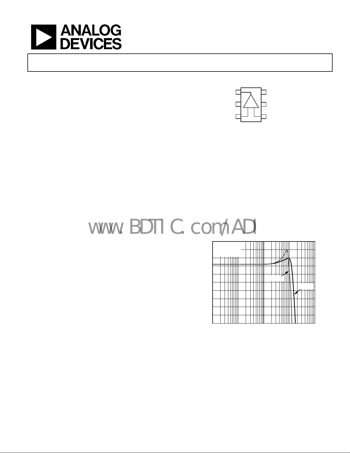
PIN CONFIGURATION
1
OUT
–V
2
S
3
+IN
Figure 1. 6-Lead SOT-23 (RJ-6)
6.3
G = +2
6.2
V
= 2V p-p
OUT
R
= RG = 499Ω
F
6.1
6.0
5.9
5.8
5.7
5.6
CLOSED-LOOP GAIN (dB)
5.5
5.4
5.3
0.1 1 10 100 1000
Figure 2. 0.1 dB Flatness
6
+V
S
5
+–
FREQUENCY (MHz )
POWER DOW N
4
–IN
VS = +5V
5709-001
= ±5V
V
S
05709-003
Rev. 0
Information furnished by Analog Devices is believed to be accurate and reliable. However, no
responsibility is assumed by Anal og Devices for its use, nor for any infringements of patents or ot her
rights of third parties that may result from its use. Specifications subject to change without notice. No
license is granted by implication or otherwise under any patent or patent rights of Analog Devices.
Trademarks and registered trademarks are the property of their respective owners.
One Technology Way, P.O. Box 9106, Norwood, MA 02062-9106, U.S.A.
Tel: 781.329.4700 www.analog.com
Fax: 781.461.3113 ©2006 Analog Devices, Inc. All rights reserved.

ADA4860-1
www.BDTIC.com/ADI
TABLE OF CONTENTS
Features.............................................................................................. 1
Power Supply Bypassing............................................................ 14
Applications....................................................................................... 1
Pin Configuration............................................................................. 1
General Description ......................................................................... 1
Revision History ............................................................................... 2
Specifications..................................................................................... 3
Absolute Maximum Ratings............................................................ 5
Thermal Resistance ...................................................................... 5
ESD Caution.................................................................................. 5
Typical Performance Characteristics ............................................. 6
Application Information................................................................ 14
REVISION HISTORY
4/06—Revision 0: Initial Version
Feedback Resistor Selection...................................................... 14
Driving Capacitive Loads.......................................................... 15
Power Down Pin......................................................................... 15
Video Amplifier.......................................................................... 15
Single-Supply Operation........................................................... 15
Optimizing Flatness and Bandwidth....................................... 16
Layout and Circuit Board Parasitics........................................ 17
Outline Dimensions....................................................................... 18
Ordering Guide .......................................................................... 18
Rev. 0 | Page 2 of 20
ADA4860-1
www.BDTIC.com/ADI
SPECIFICATIONS
VS = +5 V (@ TA = 25°C, G = +2, RL = 150 Ω referred to midsupply, CL = 4 pF, unless otherwise noted). For G = +2, RF = RG = 499 Ω and
for G = +1, R
Table 1.
Parameter Conditions Min Typ Max Unit
DYNAMIC PERFORMANCE
–3 dB Bandwidth VO = 0.2 V p-p 460 MHz
V
V
G = +1, VO = 0.2 V p-p 650 MHz
Bandwidth for 0.1 dB Flatness VO = 2 V p-p 58 MHz
V
+Slew Rate (Rising Edge) VO = 2 V p-p 695 V/μs
−Slew Rate (Falling Edge) VO = 2 V p-p 560 V/μs
Settling Time to 0.5% VO = 2 V step 8 ns
NOISE/DISTORTION PERFORMANCE
Harmonic Distortion HD2/HD3 fC = 1 MHz, VO = 2 V p-p −90/−102 dBc
f
Input Voltage Noise f = 100 kHz 4.0 nV/√Hz
Input Current Noise f = 100 kHz, +IN/−IN 1.5/7.7 pA/√Hz
Differential Gain RL = 150 Ω 0.02 %
Differential Phase RL = 150 Ω 0.03 Degrees
DC PERFORMANCE
Input Offset Voltage −13 −4.25 +13 mV
+Input Bias Current
−Input Bias Current −7 +1.0 +10 μA
Open-Loop Transresistance 400 650 kΩ
INPUT CHARACTERISTICS
Input Resistance +IN 10 MΩ
−IN 85 Ω
Input Capacitance +IN 1.5 pF
Input Common-Mode Voltage Range 1.2 to 3.7 V
Common-Mode Rejection Ratio VCM = 2 V to 3 V −52 −56 dB
POWER DOWN PIN
Input Voltage Enabled 0.5 V
Power down 1.8 V
Bias Current Enabled −200 nA
Power down 60 μA
Turn-On Time 200 ns
Turn-Off Time 3.5 μs
OUTPUT CHARACTERISTICS
Output Overdrive Recovery Time (Rise/Fall) VIN = +2.25 V to −0.25 V 60/100 ns
Output Voltage Swing RL = 75 Ω 1.2 to 3.8 V
R
R
Short-Circuit Current Sinking and sourcing 45 mA
POWER SUPPLY
Operating Range 5 12 V
Total Quiescent Current Enabled 4.5 5.2 6.5 mA
Quiescent Current POWER DOWN pin = +VS 0.2 0.5 mA
Power Supply Rejection Ratio
+PSR +VS = 4 V to 6 V, −VS = 0 V −60 −62 dB
= 550 Ω.
F
= 2 V p-p 165 MHz
O
= 0.2 V p-p, RL = 75 Ω 430 MHz
O
= 2 V p-p, RL = 75 Ω 45 MHz
O
= 5 MHz, VO = 2 V p-p −70/−76 dBc
C
−2 −1 +1 μA
= 150 Ω 1.2 to 3.8 1 to 4 V
L
= 1 kΩ 0.9 to 4.1 0.8 to 4.2 V
L
Rev. 0 | Page 3 of 20
ADA4860-1
www.BDTIC.com/ADI
VS = ±5 V (@ TA = 25°C, G = +2, RL = 150 Ω, CL = 4 pF, unless otherwise noted). For G = +2, RF = RG = 499 Ω and for G = +1, RF = 550 Ω.
Table 2.
Parameter Conditions Min Typ Max Unit
DYNAMIC PERFORMANCE
–3 dB Bandwidth VO = 0.2 V p-p 520 MHz
V
V
G = +1, VO = 0.2 V p-p 800 MHz
Bandwidth for 0.1 dB Flatness VO = 2 V p-p 125 MHz
V
+Slew Rate (Rising Edge) VO = 2 V p-p 980 V/μs
−Slew Rate (Falling Edge) VO = 2 V p-p 790 V/μs
Settling Time to 0.5% VO = 2 V step 8 ns
NOISE/DISTORTION PERFORMANCE
Harmonic Distortion HD2/HD3 fC = 1 MHz, VO = 2 V p-p −90/−102 dBc
f
Input Voltage Noise f = 100 kHz 4.0 nV/√Hz
Input Current Noise f = 100 kHz, +IN/−IN 1.5/7.7 pA/√Hz
Differential Gain RL = 150 Ω 0.02 %
Differential Phase RL = 150 Ω 0.02 Degrees
DC PERFORMANCE
Input Offset Voltage −13 −3.5 +13 mV
+Input Bias Current
−Input Bias Current −7 +1.5 +10 μA
Open-Loop Transresistance 400 700 kΩ
INPUT CHARACTERISTICS
Input Resistance +IN 12 MΩ
−IN 90 Ω
Input Capacitance +IN 1.5 pF
Input Common-Mode Voltage Range −3.8 to +3.7 V
Common-Mode Rejection Ratio VCM = ±2 V −55 −58 dB
POWER DOWN PIN
Input Voltage Enabled −4.4 V
Power down −3.2 V
Bias Current Enabled −250 nA
Power down 130 μA
Turn-On Time 200 ns
Turn-Off Time 3.5 μs
OUTPUT CHARACTERISTICS
Output Overdrive Recovery Time (Rise/Fall) VIN = ±3.0 V 45/90 ns
Output Voltage Swing RL = 75 Ω ±2 V
R
R
Short-Circuit Current Sinking and sourcing 85 mA
POWER SUPPLY
Operating Range 5 12 V
Total Quiescent Current Enabled 5 6 8 mA
Quiescent Current POWER DOWN pin = +VS 0.25 0.5 mA
Power Supply Rejection Ratio
+PSR +VS = +4 V to +6 V, −VS = −5 V −62 −64 dB
−PSR
= 2 V p-p 230 MHz
O
= 0.2 V p-p, RL = 75 Ω 480 MHz
O
= 2 V p-p, RL = 75 Ω 70 MHz
O
= 5 MHz, VO = 2 V p-p −77/−94 dBc
C
−2 −1.0 +1 μA
= 150 Ω ±2.5 ±3.1 V
L
= 1 kΩ ±3.9 ±4.1 V
L
= +5 V, −VS = −4 V to −6 V,
+V
S
POWER DOWN pin = −V
S
−58 −61 dB
Rev. 0 | Page 4 of 20
ADA4860-1
(
www.BDTIC.com/ADI
ABSOLUTE MAXIMUM RATINGS
Table 3.
Parameter Rating
Supply Voltage 12.6 V
Power Dissipation See Figure 3
Common-Mode Input Voltage −VS + 1 V to +VS − 1 V
Differential Input Voltage ±VS
Storage Temperature Range −65°C to +125°C
Operating Temperature Range −40°C to +105°C
Lead Temperature JEDEC J-STD-20
Junction Temperature 150°C
Stresses above those listed under Absolute Maximum Ratings
may cause permanent damage to the device. This is a stress
rating only; functional operation of the device at these or any
other conditions above those indicated in the operational
section of this specification is not implied. Exposure to absolute
maximum rating conditions for extended periods may affect
device reliability.
THERMAL RESISTANCE
θJA is specified for the worst-case conditions, that is, θJA is
specified for device soldered in circuit board for surface-mount
packages.
Table 4. Thermal Resistance
Package Type θJA Unit
6-lead SOT-23 170 °C/W
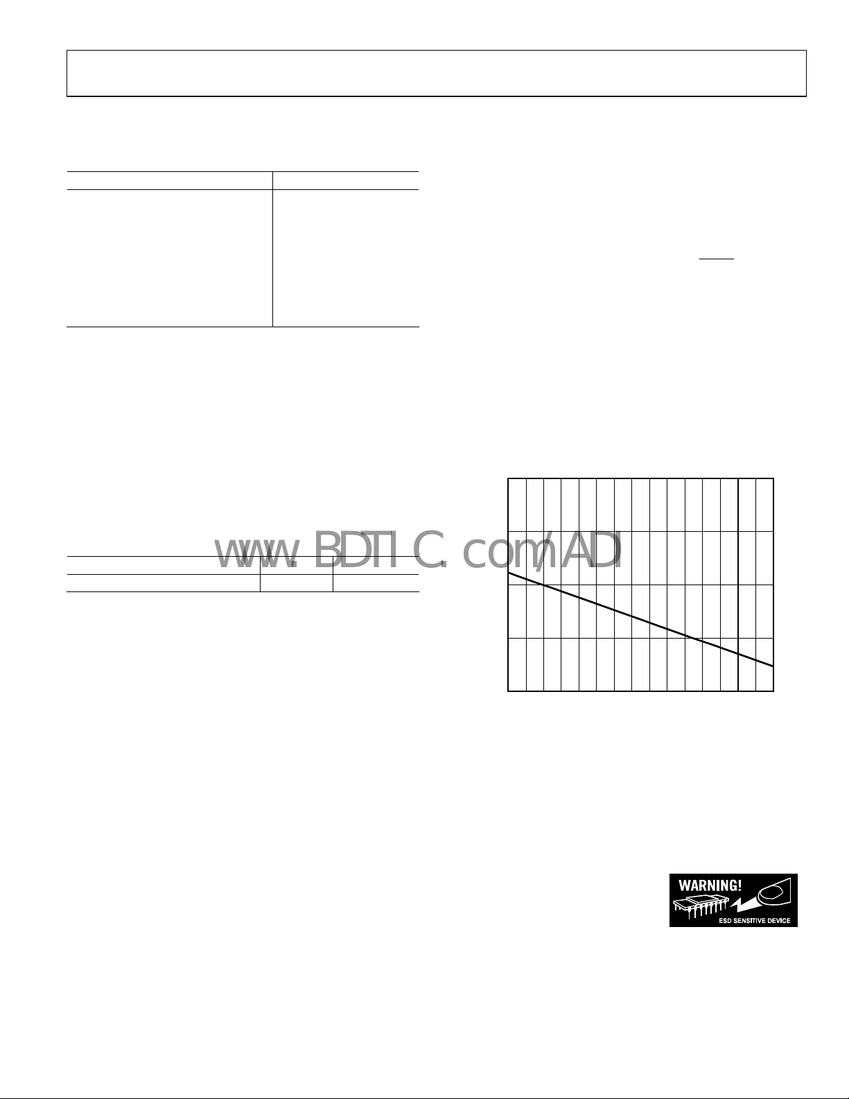
Maximum Power Dissipation
The maximum safe power dissipation for the ADA4860-1 is
limited by the associated rise in junction temperature (T
the die. At approximately 150°C, which is the glass transition
temperature, the plastic changes its properties. Even temporarily
exceeding this temperature limit can change the stresses that the
package exerts on the die, permanently shifting the parametric
performance of the amplifiers. Exceeding a junction temperature of
150°C for an extended period can result in changes in silicon
devices, potentially causing degradation or loss of functionality.
) on
J
The power dissipated in the package (P
resistor load is the total power consumed from the supply
minus the load power.
= Total Power Consumed − Load Power
P
D
D
IVP
RMS output voltages should be considered.
Airflow across the ADA4860-1 helps remove heat from the
ackage, effectively reducing θ
p
. In addition, more metal
JA
directly in contact with the package leads and through holes
under the device reduces θ
.
JA
Figure 3 shows the maximum safe power dissipation in the
ackage vs. the ambient temperature for the 6-lead SOT-23
p
(170°C/W) on a JEDEC standard 4-layer board. θ
approximations.
2.0
1.5
1.0
0.5
MAXIMUM POWER DISSIPATION (W)
0
–40 –30 –20 –10 0 110100908070605040302010
AMBIENT TEMPERAT URE (°C)
Figure 3. Maximum Power Dissipation vs. Temperature for a 4-Layer Board
) for a sine wave and a
D
V
OUT
)
CURRENTSUPPLYVOLTAGESUPPLY
–×=
R
L
JA
2
values are
05709-002
ESD CAUTION
ESD (electrostatic discharge) sensitive device. Electrostatic charges as high as 4000 V readily accumulate on
the human body and test equipment and can discharge without detection. Although this product features
proprietary ESD protection circuitry, permanent damage may occur on devices subjected to high energy
electrostatic discharges. Therefore, proper ESD precautions are recommended to avoid performance
degradation or loss of functionality.
Rev. 0 | Page 5 of 20
ADA4860-1
www.BDTIC.com/ADI
TYPICAL PERFORMANCE CHARACTERISTICS
RL = 150 Ω and CL = 4 pF, unless otherwise noted.
2
1
VS = ±5V
V
= 0.2V p-p
OUT
G = +1, RF = 550Ω
2
1
VS = 5V
V
OUT
= 0.2V p-p
G = +1, RF = 550Ω
0
–1
–2
–3
NORMALIZED GAIN (dB)
–4
–5
–6
0.1 1 10 100 1000
G = +5, RF = 348Ω, RG = 86.6Ω
G = +10, R
= RG = 499Ω
G = +2, R
F
= RG = 499Ω
G = –1, R
F
= 348Ω, RG = 38.3Ω
F
FREQUENCY (MHz)
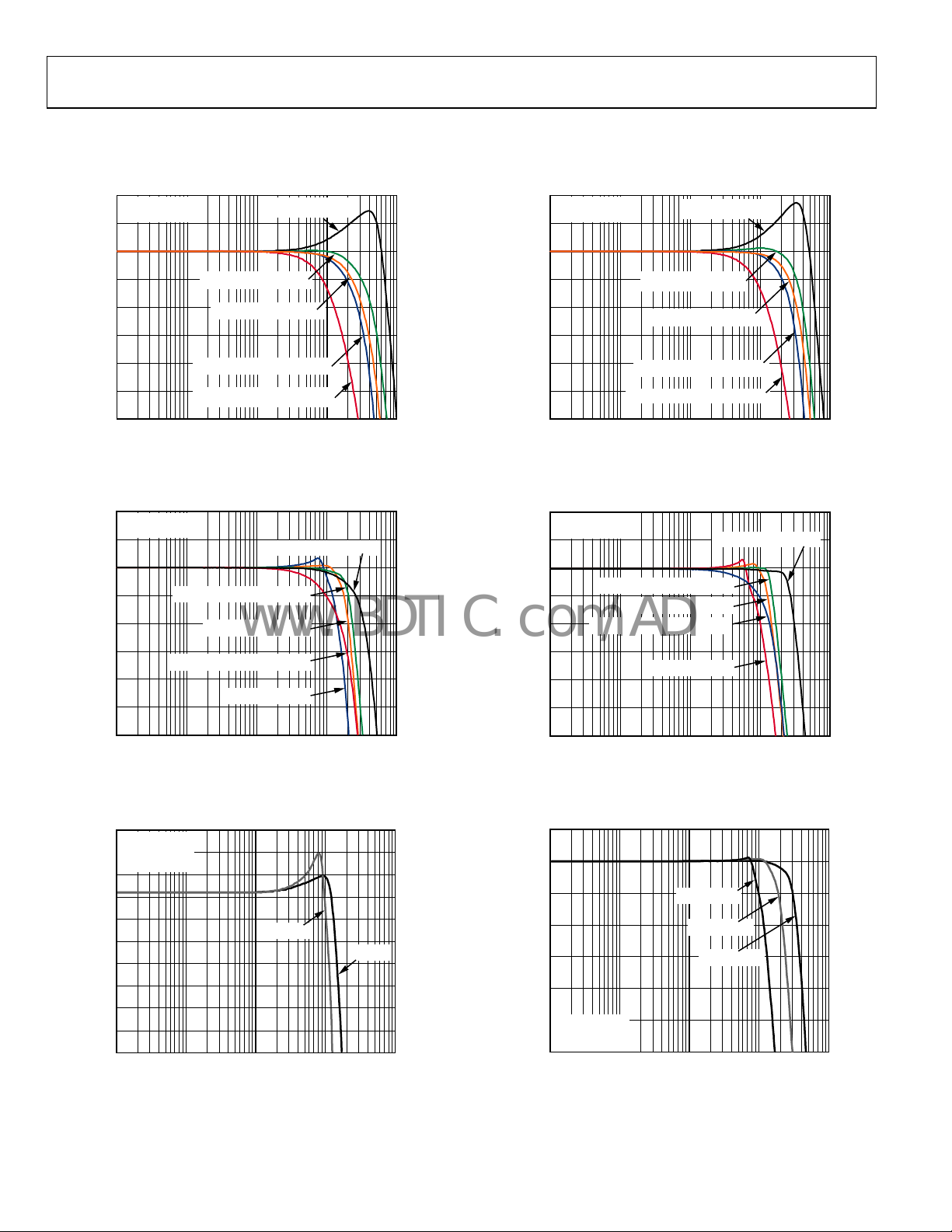
Figure 4. Small Signal Frequency Response for Various Gains
2
VS = ±5V
V
= 2V p-p
OUT
1
0
G = +5, R
–1
–2
–3
NORMALIZED GAIN (dB)
–4
–5
–6
0.1 1 10 100 1000
G = +10, R
= 348Ω, RG = 86.6Ω
F
G = +2, R
= 348Ω, RG = 38.3Ω
F
FREQUENCY (MHz )
G = –1, RF = RG = 499Ω
= RG = 499Ω
F
G = +1, RF = 550Ω
Figure 5. Large Signal Frequency Response for Various Gains
6.3
G = +2
6.2
V
= 2V p-p
OUT
R
= RG = 499Ω
F
6.1
6.0
5.9
5.8
5.7
5.6
CLOSED-LOOP GAIN (dB)
5.5
5.4
5.3
0.1 1 10 100 1000
FREQUENCY (MHz )
VS = +5V
V
= ±5V
S
Figure 6. Large Signal 0.1 dB Flatness
0
–1
–2
–3
NORMALIZED GAIN (dB)
–4
–5
05709-008
–6
0.1 1 10 100 1000
G = +5, RF = 348Ω, RG = 86.6Ω
G = +10, R
= RG = 499Ω
G = +2, R
F
= RG = 499Ω
G = –1, R
F
= 348Ω, RG = 38.3Ω
F
FREQUENCY (MHz)
05709-007
Figure 7. Small Signal Frequency Response for Various Gains
2
VS = 5V
V
= 2V p-p
OUT
1
0
–1
–2
–3
NORMALIZED GAIN (dB)
–4
–5
05709-012
–6
0.1 1 10 100 1000
G = +5, RF = 348Ω, RG = 86.6Ω
G = +2, RF = RG = 499Ω
G = +10, RF = 348Ω, RG = 38.3Ω
G = +1, RF = 550Ω
FREQUENCY (MHz)
G = –1, RF = RG = 499Ω
05709-013
Figure 8. Large Signal Frequency Response for Various Gains
7
6
5
4
3
2
CLOSED-LOOP GAIN (dB)
1
VS = ±5V
G = +2
R
= RG = 499Ω
05709-003
F
0
0.1 1 10 100 1000
V
= 4V p-p
OUT
= 2V p-p
V
OUT
V
OUT
FREQUENCY (MHz)
= 1V p-p
05709-014
Figure 9. Large Signal Frequency Response for Various Output Levels
Rev. 0 | Page 6 of 20
ADA4860-1
www.BDTIC.com/ADI
8
VS = ±5V
G = +2
7
R
= R
G
F
V
= 0.2V p-p
OUT
6
5
4
3
CLOSED-LOOP GAIN (dB)
2
1
0
0.1 1 10 100 1000
FREQUENCY (MHz)
= 301Ω
R
F
RF = 604Ω
= 499Ω
R
F
R
= 402Ω
F
05709-009
7
6
R
= 604Ω
5
4
3
2
CLOSED-LOOP GAIN (dB)
VS = ±5V
1
G = +2
R
= R
G
F
V
= 2V p-p
OUT
0
0.1 1 10 100 1000
FREQUENCY (MHz)
F
R
F
= 499Ω
RF = 301Ω
R
= 402Ω
F
05709-004
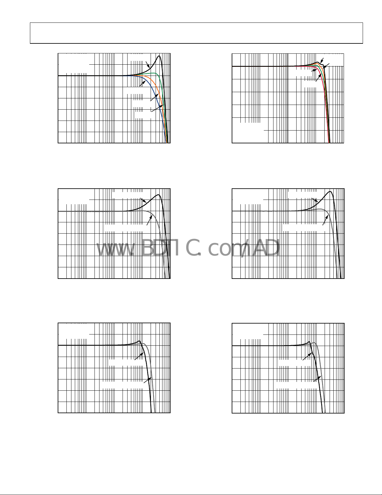
Figure 10. Small Signal Frequency Response vs. R
F
2
VS = ±5V
V
= 0.2V p-p
OUT
1
R
= 75Ω
L
0
–1
–2
–3
NORMALIZED GAIN (dB)
–4
–5
–6
0.1 1 10 100 1000
G = +1, RF = 550Ω
G = +2, R
= RG = 499Ω
F
FREQUENCY (MHz)
Figure 11. Small Signal Frequency Response for Various Gains
2
VS = ±5V
V
= 2V p-p
OUT
1
R
= 75Ω
L
0
Figure 13. Large Signal Frequency Response vs. R
F
2
VS = 5V
V
= 0.2V p-p
OUT
1
R
= 75Ω
L
0
–1
–2
–3
NORMALIZED GAIN (dB)
–4
–5
05709-006
–6
0.1 1 10 100 1000
G = +1, RF = 550Ω
G = +2, R
F
FREQUENCY (MHz)
= RG = 499Ω
05709-005
Figure 14. Small Signal Frequency Response for Various Gains
2
VS = 5V
V
= 2V p-p
OUT
1
R
= 75Ω
L
0
–1
–2
–3
NORMALIZED GAIN (dB)
–4
–5
–6
0.1 1 10 100 1000
G = +1, RF = 550Ω
G = +2, R
= RG = 499Ω
F
FREQUENCY (MHz)
05709-015
Figure 12. Large Signal Frequency Response for Various Gains
Rev. 0 | Page 7 of 20
–1
–2
–3
NORMALIZED GAIN (dB)
–4
–5
–6
0.1 1 10 100 1000
G = +1, RF = 550Ω
G = +2, R
= RG = 499Ω
F
FREQUENCY (MHz)
Figure 15. Large Signal Frequency Response for Various Gains
05709-016

ADA4860-1
–
–
–
–
–
–
www.BDTIC.com/ADI
–50
40
VS = ±5V
G = +1
R
= 550Ω
F
40
–50
VS = ±5V
G = +2
R
= RG = 499Ω
F
–60
–70
V
= 3V p-p, HD2
OUT
–80
DISTO RTIO N (dBc)
–90
–100
–110
1 10 100
V
= 3V p-p, HD3
OUT
V
OUT
FREQUENCY (MHz )
V
= 2V p-p, HD2
OUT
= 2V p-p, HD3
Figure 16. Harmonic Distortion vs. Frequency
40
VS = 5V
G = +1
R
= 550Ω
–50
F
–60
–70
–80
DISTORTION (dBc)
–90
V
= 2V p-p, HD3
OUT
V
= 2V p-p, HD2
OUT
V
OUT
V
= 1V p-p, HD3
OUT
= 1V p-p, HD2
–60
V
–70
–80
DISTO RTIO N (dBc)
–90
–100
05709-017
–110
= 3V p-p, HD2
OUT
1 10 100
V
= 2V p-p, HD2
OUT
V
= 2V p-p, HD3
OUT
FREQUENCY (MHz)
= 3V p-p, HD3
V
OUT
05709-041
Figure 19. Harmonic Distortion vs. Frequency
40
VS = 5V
G = +2
R
= RG = 499Ω
–50
F
V
= 2V p-p, HD3
–60
V
OUT
–70
–80
DISTORTION (dBc)
–90
OUT
= 2V p-p, HD2
V
OUT
= 1V p-p, HD3
V
OUT
= 1V p-p, HD2
–100
–110
1 10 100
FREQUENCY (MHz )
Figure 17. Harmonic Distortion vs. Frequency
40
G = +1
R
= 550Ω
F
R
= 100Ω
–50
L
V
= 2V p-p, HD2
–60
V
–70
–80
DISTO RTIO N (dBc)
–90
–100
–110
1 10 100
V
OUT
= +5V
S
OUT
V
= ±5V
S
= 1V p-p, HD2
FREQUENCY (MHz)
V
= 1V p-p, HD3
OUT
V
= +5V
S
V
= 2V p-p, HD3
OUT
V
= ±5V
S
Figure 18. Harmonic Distortion vs. Frequency for Various Supplies
–100
05709-018
–110
1 10 100
FREQUENCY (MHz)
05709-019
Figure 20. Harmonic Distortion vs. Frequency
40
G = +2
R
= RG = 499Ω
F
R
= 100Ω
–50
L
–60
V
OUT
V
= ±5V
–70
–80
DISTORTION (dBc)
–90
–100
05709-061
–110
S
1 10 100
V
OUT
V
= 2V p-p, HD2
S
FREQUENCY (MHz )
= 1V p-p, HD2
= +5V
= 1V p-p, HD3
V
OUT
V
= +5V
S
= 2V p-p, HD3
V
OUT
V
= ±5V
S
05709-062
Figure 21. Harmonic Distortion vs. Frequency for Various Supplies
Rev. 0 | Page 8 of 20

ADA4860-1
www.BDTIC.com/ADI
200
VS = +5V
2.7
200
2.7
VS = +5V
100
VS = ±5V
0
= 5V
S
±V
OUTPUT VO LTAGE (mV)
–100
G = +1
= 0.2V p-p
V
OUT
= 550Ω
R
F
TIME = 5n s/DIV
–200
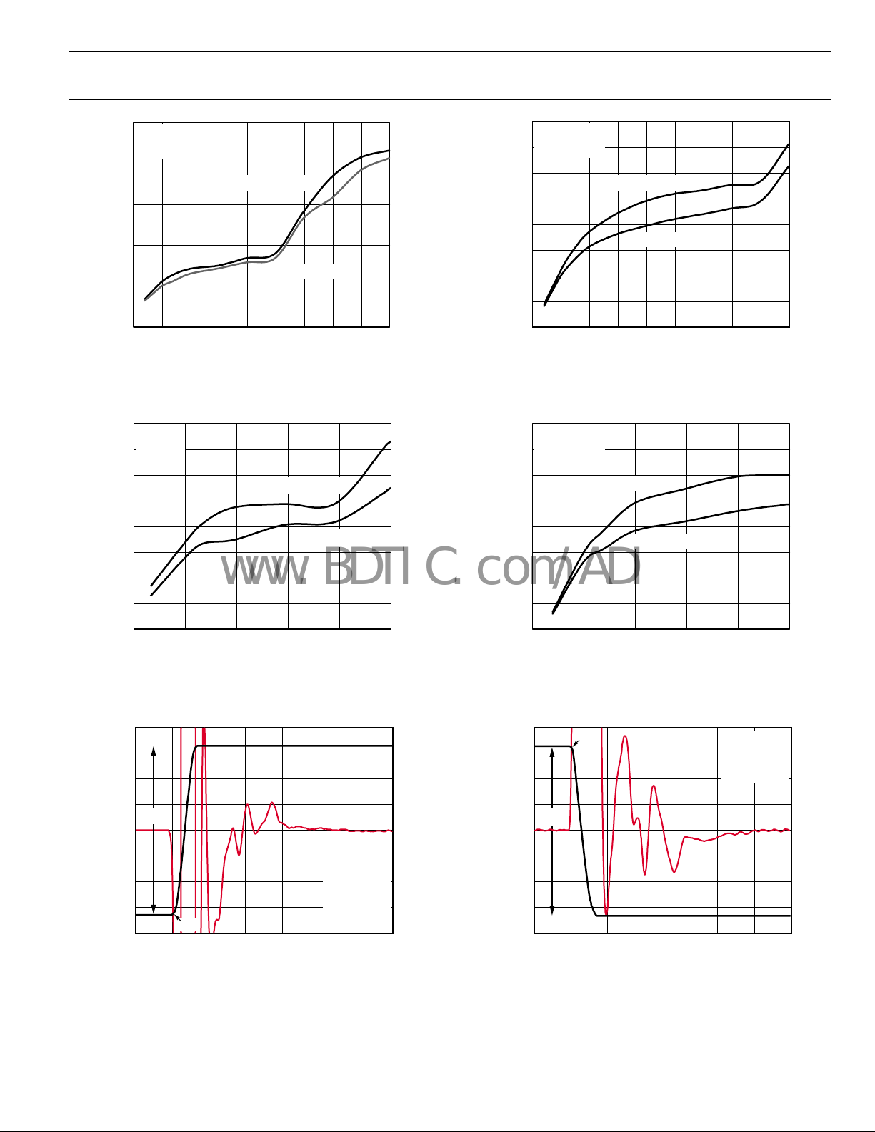
Figure 22. Small Signal Transient Response for Various Supplies
OUTPUT VO LTAGE (mV)
200
100
0
–100
–200
CL = 9pF
C
= 4pF
L
VS = ±5V
G = +1
= 0.2V p-p
V
OUT
= 550Ω
R
F
TIME = 5ns/DIV
C
= 6pF
L
2.6
2.5
2.4
2.3
100
= ±5V
V
= 0V
S
0
= 5V
S
= 5V, –V
S
+V
OUTPUT VOLTAGE (V)
05709-033
±V
OUTPUT VO LTAGE (mV)
–100
–200
S
G = +2
= 0.2V p-p
V
OUT
= RG = 499Ω
R
F
TIME = 5ns/DIV
2.6
2.5
2.4
2.3
OUTPUT VOLTAGE (V)
= 0V
S
= 5V, –V
S
+V
05709-020
Figure 25. Small Signal Transient Response for Various Supplies
200
CL = 9pF
= 6pF
C
L
100
CL = 4pF
0
OUTPUT VO LTAGE (mV)
–100
VS = ±5V
G = +2
= 0.2V p-p
V
OUT
= RG = 499Ω
R
F
05709-034
–200
TIME = 5ns/DIV
05709-021
Figure 23. Small Signal Transient Response for Various Capacitor Loads
2.7
C
= 6pF
L
= 4pF
C
L
2.6
CL = 9pF
2.5
OUTPUT VOLTAGE (V)
2.4
VS = 5V
G = +1
= 0.2V p-p
V
OUT
= 550Ω
R
F
2.3
TIME = 5n s/DIV
05709-035
Figure 24. Small Signal Transient Response for Various Capacitor Loads
Figure 26. Small Signal Transient Response for Various Capacitor Loads
2.7
CL = 9pF
= 6pF
C
L
2.6
CL = 4pF
2.5
OUTPUT VOLTAGE (V)
2.4
VS = 5V
G = +2
= 0.2V p-p
V
OUT
= RG = 499Ω
R
F
TIME = 5ns/DIV
2.3
05709-022
Figure 27. Small Signal Transient Response for Various Capacitor Loads
Rev. 0 | Page 9 of 20

ADA4860-1
www.BDTIC.com/ADI
1.5
1.0
VS = ±5V
V
= +5V
S
4.0
3.5
1.5
1.0
V
= ±5V
S
VS = +5V
4.0
3.5
0.5
0
= 5V
S
±V
–0.5
OUTPUT VOLTAGE (V)
G = +1
–1.0
–1.5
= 2V p-p
V
OUT
= 550Ω
R
F
TIME = 5ns/DIV
Figure 28. Large Signal Transient Response for Various Supplies
1.5
OUTPUT VOLTAGE (V)
CL = 9pF
1.0
0.5
0
–0.5
–1.0
–1.5
C
= 6pF
L
= 4pF
C
L
VS = ±5V
G = +1
= 2V p-p
V
OUT
= 550Ω
R
F
TIME = 5ns/DIV
3.0
2.5
2.0
1.5
1.0
0.5
= 0V
S
0
= 5V
S
= 5V, –V
S
+V
OUTPUT VOLTAGE (V)
05709-036
±V
–0.5
OUTPUT VOLTAGE (V)
G = +2
–1.0
–1.5
= 2V p-p
V
OUT
= RG = 499Ω
R
F
TIME = 5ns/DIV
3.0
2.5
2.0
1.5
1.0
OUTPUT VOLTAGE (V)
= 0V
S
= 5V, –V
S
+V
05709-023
Figure 31. Large Signal Transient Response for Various Supplies
1.5
= 9pF CL = 6pF
C
L
1.0
0.5
0
–0.5
OUTPUT VOLTAGE (V)
–1.0
05709-037
–1.5
CL = 4pF
VS = ±5V
G = +2
= 2V p-p
V
OUT
= RG = 499Ω
R
F
TIME = 5ns/DIV
05709-024
Figure 29. Large Signal Transient Response for Various Capacitor Loads
4.0
CL = 9pF
3.5
3.0
2.5
2.0
OUTPUT VOLTAGE (V)
1.5
1.0
C
= 6pF
L
C
= 4pF
L
VS = 5V
G = +1
= 2V p-p
V
OUT
= 550Ω
R
F
TIME = 5ns/DIV
05709-039
Figure 30. Large Signal Transient Response for Various Capacitor Loads
Rev. 0 | Page 10 of 20
Figure 32. Large Signal Transient Response for Various Capacitor Loads
4.0
= 9pF
C
L
3.5
3.0
2.5
2.0
OUTPUT VOLTAGE (V)
1.5
1.0
C
= 6pF
L
CL = 4pF
VS = 5V
G = +2
= 2V p-p
V
OUT
= RG = 499Ω
R
F
TIME = 5ns/DIV
05709-025
Figure 33. Large Signal Transient Response for Various Capacitor Loads
ADA4860-1
www.BDTIC.com/ADI
2500
VS = ±5V
G = +1
R
= 550Ω
F
2000
POSITIVE SL EW RATE
1500
1000
SLEW RATE (V/µs)
500
0
04
INPUT VOLTAGE (V p-p)
NEGATIVE SL EW RATE
05709-043
4.03.53.02.52. 01.51.00. 5
.5
Figure 34. Slew Rate vs. Input Voltage
SLEW RATE (V/µs)
1600
1400
1200
1000
800
600
400
200
VS = ±5V
G = +2
R
= RG = 499Ω
F
POSITIVE SLEW RATE
NEGATIVE S LEW RATE
0
02.252.001.751.501.251.000.750.500.25
INPUT VOLTAGE (V p-p)
Figure 37. Slew Rate vs. Input Voltage
05709-028
900
800
700
600
500
400
SLEW RATE (V/µs)
300
200
100
1.00
0.75
0.50
0.25
0
V
= 5V
S
G = +1
R
= 550Ω
F
02.52.01.51.00.5
INPUT VOLTAGE (V p-p)
Figure 35. Slew Rate vs. Input Voltage
1V
POSITIVE SLEW RATE
NEGATIVE SLEW RATE
V
IN
900
VS = 5V
G = +2
800
R
= RG = 499Ω
F
700
600
500
400
SLEW RATE (V/µs)
300
200
05709-026
100
01.251.000.750.500.25
POSITIVE SLEW RATE
NEGATIVE S LEW RATE
INPUT VOLTAGE (V p-p)
05709-029
Figure 38. Slew Rate vs. Input Voltage
1.00
0.75
0.50
0.25
0
t = 0s
1V
VS = ±5V
G = +2
V
= 2V p-p
OUT
R
= RG = 499Ω
F
TIME = 5ns/DIV
–0.25
SETTLING TIME (%)
–0.50
–0.75
–1.00
t = 0s
VS = ±5V
G = +2
V
= 2V p-p
OUT
R
= RG = 499Ω
F
TIME = 5ns/DIV
05709-027
Figure 36. Settling Time Rising Edge
Rev. 0 | Page 11 of 20
–0.25
SETTLING TIME (%)
–0.50
–0.75
–1.00
V
IN
Figure 39. Settling Time Falling Edge
05709-030

ADA4860-1
www.BDTIC.com/ADI
30
25
20
15
10
INPUT VOLTAGE NO ISE (nV/ Hz)
5
0
10 100 1k 10k 100k 1M 10M 100M
FREQUENCY (Hz)
VS = ±5V, +5V
Figure 40. Input Voltage Noise vs. Frequency
05709-031
110
100
90
80
70
60
50
40
30
20
INPUT CURRENT NO ISE (pA/ Hz)
10
0
10 100 1k 10k 100k 1M 10M 100M
NONINVERTI NG INPUT
INVERTING INPUT
FREQUENCY (Hz)
VS = ±5V, +5V
Figure 43. Input Current Noise vs. Frequency
05709-032
0
VS = ±5V
G = +2
–10
–20
–30
–40
–50
POWER SUPPLY REJECTI ON (dB)
–60
–70
0.1 1 10 100 1000
Figure 41. Power Supply Reje
–PSR
+PSR
FREQUENCY (MHz )
ction vs. Frequency
OUTPUT AND INP UT VOLT AGE (V)
6
5
4
3
2
1
0
–1
–2
–3
–4
–5
–6
0 1000900800700600500400300200100
OUTPUT
VOLTAGE
INPUT VOLTAGE × 2
TIME (ns)
VS = ±5V
G = +2
R
= RG = 499Ω
F
f = 1MHz
0
VS = ±5V
= 200mV rms
V
OUT
= 560Ω
R
–10
F
–20
–30
–40
–50
COMMON-MODE REJECTION (dB)
–60
05709-053
–70
0.1 1 10 100 1000
FREQUENCY (MHz )
05709-055
Figure 44. Common-Mode Rejection vs. Frequency
5.5
5.0
4.5
4.0
3.5
3.0
2.5
2.0
1.5
1.0
0.5
OUTPUT AND INP UT VOLT AGE (V)
0
05709-040
–0.5
0 1000900800700600500400300200100
VOLTAGE
INPUT VOLTAGE × 2
OUTPUT
TIME (ns)
VS = 5V
G = +2
R
= RG = 499Ω
F
f = 1MHz
05709-042
Figure 42. Output Ove
rdrive Recovery
Rev. 0 | Page 12 of 20
Figure 45. Output Ove
rdrive Recovery

ADA4860-1
V
www.BDTIC.com/ADI
1000
VS = ±5V
G = +2
0
40
30
100
PHASE
10
TRANSIMPEDANCE (kΩ)
1
0.1
0.01 0. 1 1 10 100 1000
FREQUENCY (MHz)
TRANSIMPEDANCE
Figure 46. Transimpedance and Phase vs. Frequency
6.5
6.0
5.5
5.0
VS = ±5V
= +5V
V
S
–45
–90
–135
–180
PHASE (Degrees)
05709-054
20
10
(mV)
OS
0
–10
INPUT
–20
–30
–40
VS = ±5V VS = +5V
–5 –4 –3 –2 –1 0 1 2 435
Figure 49. Input V
VCM (V)
vs. Common-Mode Voltage
OS
7.0
6.5
6.0
5.5
5.0
05709-058
4.5
TOTAL SUPPLY CURRENT (mA)
4.0
–40 –25 –10 5 20 35 50 65 80 95 110 125
TEMPERATURE (° C)
Figure 47. Supply Current at Various Supplies vs. Temperature
10
8
6
4
2
0
–2
–4
INPUT BIAS CURRENT (µA)
–6
–8
–10
VS = ±5V
VS = +5V
–5 –4 –3 –2 –1 0 1 2 3 4 5
OUTPUT VO LTAGE (V )
Figure 48. Inverting Input Bias Current vs. Output Voltage
TOTAL SUPPLY CURRENT (mA)
4.5
05709-059
4.0
41111098765
SUPPLY VOLTAGE (V)
05709-057
2
Figure 50. Supply Current vs. Supply Voltage
05709-056
Rev. 0 | Page 13 of 20

ADA4860-1
V
V
www.BDTIC.com/ADI
APPLICATION INFORMATION
POWER SUPPLY BYPASSING
Attention must be paid to bypassing the power supply pins of
the ADA4860-1. High quality capacitors with low equivalent
series resistance (ESR), such as multilayer ceramic capacitors
(MLCCs), should be used to minimize supply voltage ripple
and power dissipation. Generally, a 10 μF tantalum capacitor
located in close proximity to the ADA4860-1 is required to
provide good decoupling for lower frequency signals. In
addition, a 0.1 μF decoupling multilayer ceramic chip capacitor
(MLCC) should be located as close to each of the power supply
pins as is physically possible, no more than ⅛ inch away. The
ground returns should terminate immediately into the ground
plane. Locating the bypass capacitor return close to the load
return minimizes ground loops and improves performance.
FEEDBACK RESISTOR SELECTION
The feedback resistor has a direct impact on the closed-loop
bandwidth and stability of the current feedback op amp circuit.
Reducing the resistance below the recommended value can
make the amplifier response peak and even become unstable.
Increasing the size of the feedback resistor reduces the closedloop bandwidth.
q
uickly determining the feedback and gain set resistor values
and bandwidth for common gain configurations.
Table 5. Recommended Values and Frequency Performance
Gain RF (Ω) RG (Ω)
+1 550 N/A 800 165 40
−1 499 499 400 400 80
+2 499 499 520 230 125
+5 348 86.6 335 265 100
+10 348 38.3 165 195 28
1
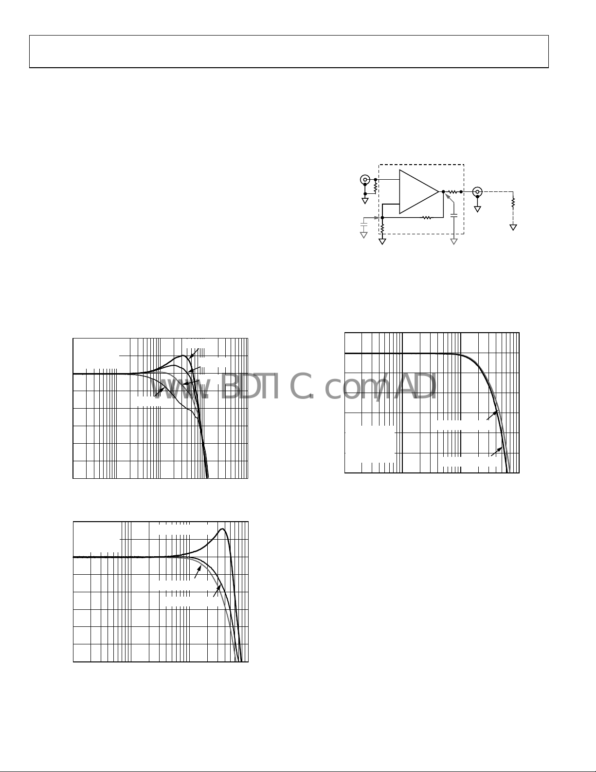
Conditions: VS = ±5 V, TA = 25°C, RL = 150 Ω.
Tabl e 5 provides a convenient reference for
Large
W
−3 dB
LS BW
(MHz)
Signal
0.1 dB
F
latness
−3 dB
SS B
(MHz)
1
Figure 51 and Figure 52 show the typical noninverting and
inverting configurations and the recommended bypass
capacitor values.
+
S
10µF
+
0.1µF
V
IN
R
IN
+
ADA4860-1
–
R
F
G
Figure 51. Noninverting Gain
R
G
–
ADA4860-1
+
Figure 52. Inverting Gain
0.1µF
10µF
–V
S
R
F
+V
S
–V
S
+
10µF
+
0.1µF
0.1µF
10µF
V
OUT
5709-010
V
OUT
+
5709-011
Rev. 0 | Page 14 of 20
ADA4860-1
T
www.BDTIC.com/ADI
DRIVING CAPACITIVE LOADS
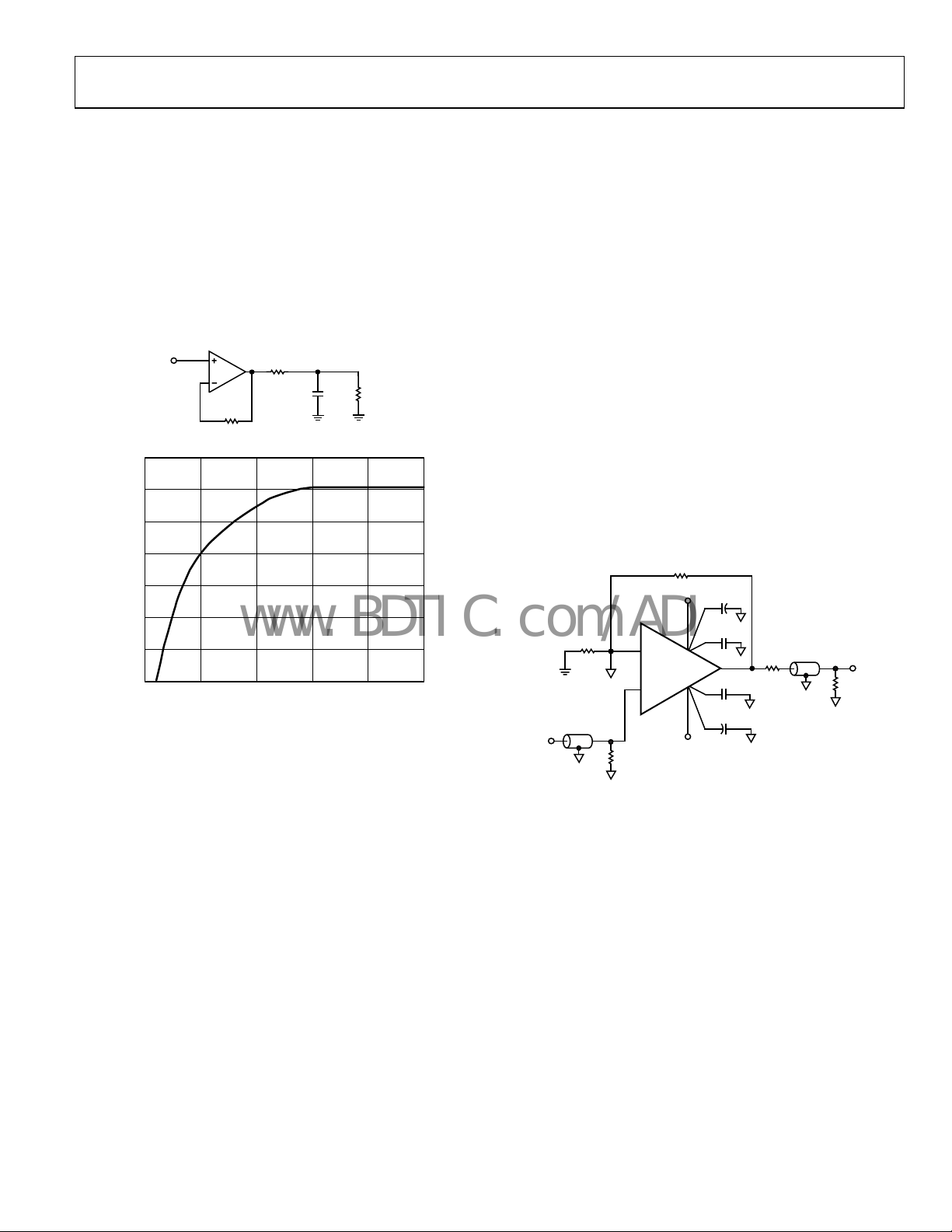
If driving loads with a capacitive component is desired, the best
frequency response is obtained by the addition of a small series
resistance, as shown in Figure 53. Figure 54 shows the optimum
val
ue for R
a 50 MHz, 50% duty cycle pulse, with an amplitude of 200 mV p-p.
The criteria for R
approximately 1 dB of peaking in small signal frequency
response. It is worth noting that the frequency response of the
circuit can be dominated by the passive roll-off of R
SERIES RESISTANCE (Ω)
vs. capacitive load. The test was performed with
SERIES
selection was based on maintaining
SERIES
and CL.
SERIES
ADA4860-1
V
IN
Figure 53. Driving Capacitive Loads
14
12
10
8
6
4
2
0
05
Figure 54. Recommended R
R
SERIES
R
F
750Ω
CAPACITIVE LOAD (pF )
C
SERIES
R
L
L
vs. Capacitive Load
05709-052
05709-060
040302010
POWER DOWN PIN
The ADA4860-1 is equipped with a power-down function.
The POWER DOWN pin allows the user to reduce the quiescent
supply current when the amplifier is not being used. The
power-down threshold levels are derived from the voltage
applied to the −V
pin. When used in single-supply applications,
S
this is especially useful with conventional logic levels. The
amplifier is powered down when the voltage applied to the
POWER DOWN pin is greater than (−V
+ 0.5 V). The
S
amplifier is enabled whenever the POWER DOWN pin is left
open, or the voltage on the POWER DOWN pin is less than
(−V
+ 0.5 V). If the POWER DOWN pin is not used, it should
S
be connected to the negative supply.
VIDEO AMPLIFIER
With low differential gain and phase errors and wide 0.1 dB
flatness, the ADA4860-1 is an ideal solution for consumer and
professional video applications. Figure 55 shows a typical video
dr
iver set for a noninverting gain of +2, where R
The video amplifier input is terminated into a shunt 75 Ω resistor.
At the output, the amplifier has a series 75 Ω resistor for
impedance matching to the video load.
R
F
+V
S
10µF
+
–V
S
0.1µF
0.1µF
10µF
+
iver Schematic
R
G
–
ADA4860-1
+
75Ω
CABLE
V
IN
75Ω
Figure 55. Video Dr
75Ω
CABLE
= RG = 499 Ω.
F
75Ω
V
75Ω
OU
05709-038
Rev. 0 | Page 15 of 20
SINGLE-SUPPLY OPERATION
Single-supply operation can present certain challenges for the
designer. For a detailed explanation on op amp single-supply
operation, see Application Note AN-581.
ADA4860-1
A
www.BDTIC.com/ADI
OPTIMIZING FLATNESS AND BANDWIDTH
When using the ADA4860-1, a variety of circuit conditions and
parasitics can affect peaking, gain flatness, and −3 dB
bandwidth. This section discusses how the ADA4860-1 small
signal responses can be dramatically altered with basic circuit
changes and added stray capacitances, see the
cuit Board Parasitics section for more information.
Cir
Layout and
The impact of resistor case sizes was observed using the circuit
drawn in Figure 58. The types and sizes chosen were 0402 case
d thin film and 1206 thick film. All other measurement
size
conditions were kept constant except for the case size and
resistor composition.
DASH LINE I S PLANE CL EAR OUT ARE
(EXCEPT SUPPLY PI NS) DURING P C LAYOUT.
Particularly with low closed-loop gains, the feedback resistor
(R
) effects peaking and gain flatness. However, with gain = +1,
f
−3 dB bandwidth varies slightly, while gain = +2 has a much
larger variation. For gain = +1, Figure 56 shows the effect that
v
arious feedback resistors have on frequency response. In
Figure 56, peaking is wide ranging yet −3 dB bandwidths vary
y only 6%. In this case, the user must pick what is desired:
b
more peaking or flatter bandwidth. Figure 57 shows gain = +2
b
andwidth and peaking variations vs. R
delta vs. R
increase was approximately 17%. As RF is reduced
L
and RL. Bandwidth
F
from 560 Ω to 301 Ω, the −3 dB bandwidth changes 49%, with
excessive compromises in peaking, see
ndwidth variations vs. R
= +2 ba
2
VS = ±5V
G = +1
1
= 0.1V p-p
V
OUT
= 100Ω
R
L
0
–1
= 1.5kΩ
R
–2
–3
NORMALIZED GAIN (dB)
–4
–5
–6
1 10010 100001000
Figure 56. Small Signal Frequency Response vs. R
2
VS = ±5V
G = +2
1
= 0.1V p-p
V
OUT
= R
R
G
F
0
F
FREQUENCY (MHz)
Figure 57. For more gain
, see Figure 10 and Figure 13.
F
R
= 560Ω
F
= 680Ω
R
F
R
= 910Ω
F
F
RF = 301Ω, RL = 100Ω
05709-044
ADDED C
EXAMPLE
+
49.9Ω
–
J
R
G
49.9Ω
R
F
ADDED C
EXAMPLE
LOAD
50Ω
05709-049
Figure 58. Noninverting Gain Setup for Illustration of
P
arasitic Effects, 50 Ω System, R
= 100 Ω
L
In Figure 59, a slight −3 dB bandwidth delta of approximately
+10% can be seen going from a small-to-large case size. The
increase in bandwidth with the larger 1206 case size is caused
by an increase in parasitic capacitance across the chip resistor.
1
0
–1
–2
–3
VS = ±5V
–4
NORMALIZED GAIN (dB)
G = +2
= 0.1V p-p
V
OUT
= RF= 560Ω
R
G
–5
= 100Ω
R
L
–6
1 10010 1000
FREQUENCY (MHz )
Figure 59. Small Signal Frequency R
1206 RESISTOR SIZE
0402 RESISTO R SIZE
05709-046
esponse vs. Resistor Size
–1
= 560Ω, RL = 100Ω
R
–2
–3
NORMALIZED GAIN (dB)
–4
–5
–6
1 10010 1000
Figure 57. Small Signal Frequency Response vs. R
F
R
= 560Ω, RL = 1kΩ
F
FREQUENCY (MHz)
vs. RL
F
05709-045
Rev. 0 | Page 16 of 20
ADA4860-1
www.BDTIC.com/ADI
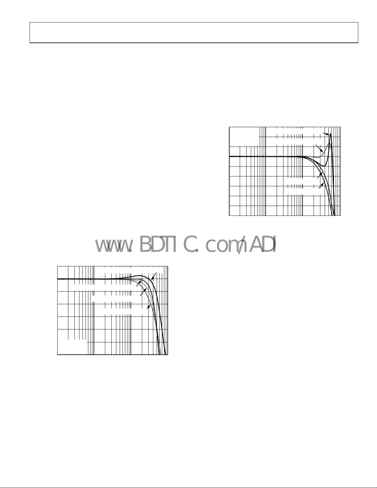
LAYOUT AND CIRCUIT BOARD PARASITICS
Careful attention to printed circuit board (PCB) layout prevents
associated board parasitics from becoming problematic and
affecting gain flatness and −3 dB bandwidth. In the printed
circuit environment, parasitics around the summing junction
(inverting input) or output pins can alter pulse and frequency
response. Parasitic capacitance can be unintentionally created
on a PC board via two parallel metal planes with a small vertical
separation (in FR4). To avoid parasitic problems near the
summing junction, signal line connections between the
feedback and gain resistors should be kept as short as possible
to minimize the inductance and stray capacitance. For similar
reasons, termination and load resistors should be located as
close as possible to the respective inputs. Removing the ground
plane on all layers from the area near and under the input and
output pins reduces stray capacitance.
To illustrate the affects of parasitic capacitance, a small
capacitor of 0.4 pF from the amplifiers summing junction
(inverting input) to ground was intentionally added. This was
done on two boards with equal and opposite gains of +2 and −2.
Figure 60 reveals the effects of parasitic capacitance at the
s
umming junction for both noninverting and inverting gain
circuits. With gain = +2, the additional 0.4 pF of added
capacitance created an extra 43% −3 dB bandwidth extension,
plus some extra peaking. For gain = −2, a 5% increase in −3 dB
bandwidth was created with an extra 0.4 pF on summing
junction.
1
0
–1
–2
–3
G = –2, R
G = +2, RF = 560Ω, CJ = 0.4pF EXTRA
= 402Ω, CJ = 0.4pF EXTRA
F
= 402Ω, CJ = 0pF
G = –2, R
F
= 560Ω, CJ = 0pF
G = +2, R
F
In a second test, 5.6 pF of capacitance was added directly at the
utput of the gain = +2 amplifier. Figure 61 shows the results.
o
xtra output capacitive loading on the ADA4860-1 also causes
E
bandwidth extensions, as seen in
ain = +2 circuit is more pronounced with lighter resistive
g
Figure 61. The effect on the
loading (1 kΩ). For pulse response behavior with added output
capacitances, see
Figure 23, Figure 24, Figure 26, Figure 27,
Figure 29, Figure 30, Figure 32, and Figure 33.
3
VS = ±5V
G = +2
2
= 0.1V p-p
V
OUT
= RG = 560Ω
R
F
1
0
–1
–2
–3
NORMALIZED GAIN (dB)
–4
–5
–6
1 10010 1000
RL = 1kΩ, CL = 5.6pF EXTRA
R
= 100Ω, CL = 5.6pF E XTRA
L
R
= 1kΩ, CL = 0pF
L
R
= 100Ω, CL = 0pF
L
FREQUENCY (MHz )
05709-048
Figure 61. Small Signal Frequency Response vs. Output Capacitive Load
For more information on high speed board layout, go to:
www.analog.com and
www.analog.com/library/analogDialogue/archives/3909/l
ayout.html.
–4
NORMALIZED GAIN (dB)
–5
VS = ±5V
= 0.1V p-p
V
OUT
= 100Ω
R
L
–6
1 10010 1000
FREQUENCY (MHz )
05709-047
Figure 60. Small Signal Frequency Response vs.
Added Summing Junction C
apacitance
Rev. 0 | Page 17 of 20
ADA4860-1
www.BDTIC.com/ADI
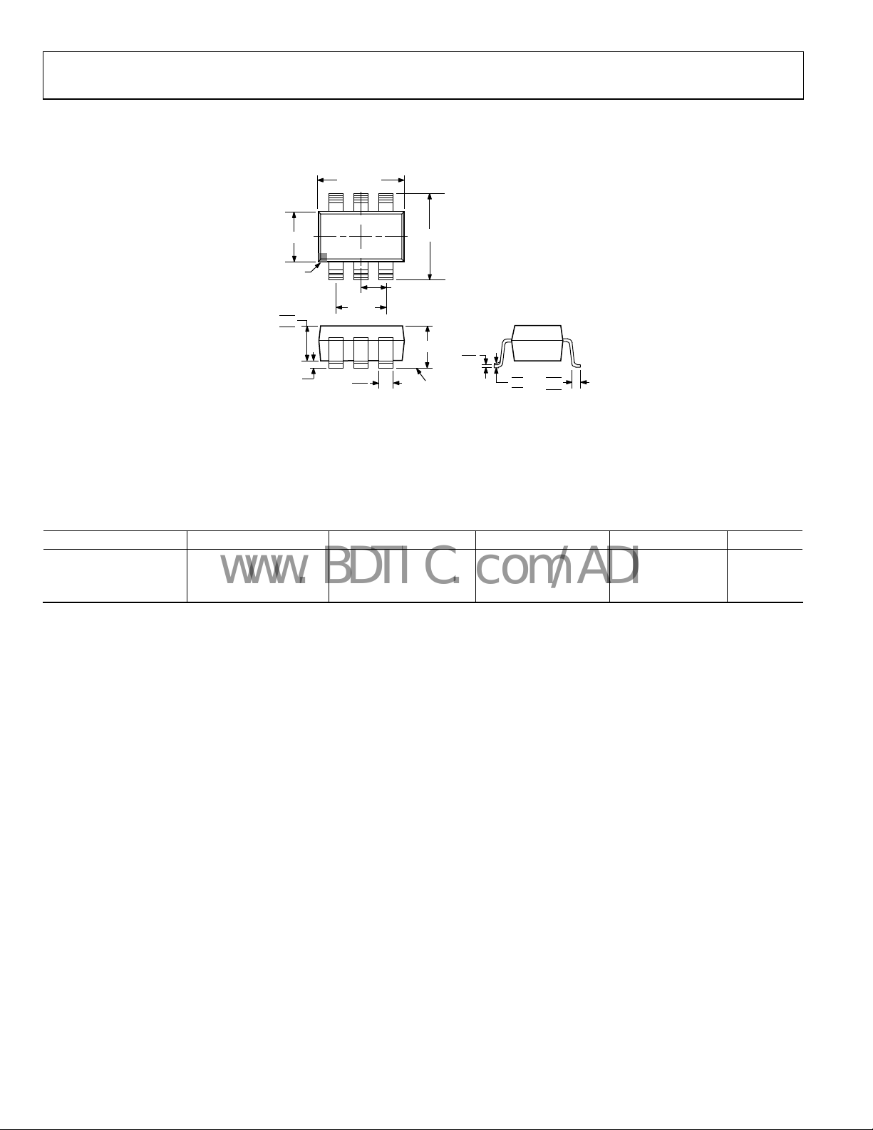
OUTLINE DIMENSIONS
2.90 BSC
4526
1.60 BSC
PIN 1
INDICATOR
1.30
1.15
0.90
0.15 MAX
1 3
1.90
BSC
0.50
0.30
2.80 BSC
0.95 BSC
1.45 MAX
SEATING
PLANE
0.22
0.08
10°
0.60
4°
0.45
0°
0.30
COMPLIANT TO JEDEC STANDARDS MO-178-AB
Figure 62. 6-Lead Plastic Surface-Mount Package [SOT-23]
(RJ-6)
ensions shown in millimeters
Dim
ORDERING GUIDE
Model Temperature Range Package Description Ordering Quantity Package Option Branding
ADA4860-1YRJZ-RL
ADA4860-1YRJZ-RL7
ADA4860-1YRJZ-R2
1
Z = Pb-free part.
1
–40°C to +105°C 6-Lead SOT-23 10,000 RJ-6 HKB
1
–40°C to +105°C 6-Lead SOT-23 3,000 RJ-6 HKB
1
–40°C to +105°C 6-Lead SOT-23 250 RJ-6 HKB
Rev. 0 | Page 18 of 20

ADA4860-1
www.BDTIC.com/ADI
NOTES
Rev. 0 | Page 19 of 20

ADA4860-1
www.BDTIC.com/ADI
NOTES
©2006 Analog Devices, Inc. All rights reserved. Trademarks and
registered trademarks are the property of their respective owners.
D05709-0-4/06(0)
Rev. 0 | Page 20 of 20
 Loading...