

Single-Supply, Fixed G = 2, High Speed,
www.BDTIC.com/ADI
FEATURES
Integrated charge pump
Supply range: 3 V to 5.5 V
Output range: −3.3 V to −1.8 V
50 mA maximum output current at −3 V for external use
High speed amplifiers
−3 dB bandwidth: 195 MHz
Slew rate: 740 V/μs
0.1 dB gain flatness: 60 MHz
0.1% settling time: 20 ns
Low power
Total quiescent current: 38 mA
Power-down feature
High input common-mode voltage range
−1.8 V to +3.8 V at +5 V supply
Current feedback architecture
Differential gain error: 0.01%
Differential phase error: 0.02°
Available in 16-lead LFCSP
APPLICATIONS
Professional video
Consumer video
Imaging
Active filters
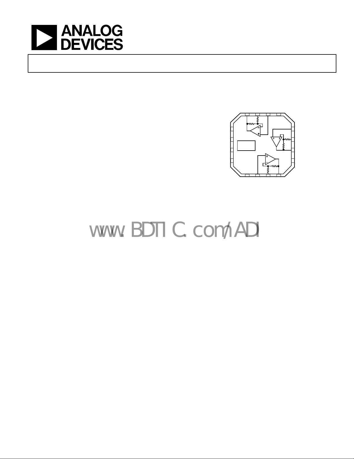
Video Amplifier with Charge Pump
ADA4859-3
CONNECTION DIAGRAM
ADA4859-3
OUT1
–IN1
+IN1
NC
16 15 14 13
12
+V
1
S
2C1_a
CHARGE
PUMP
3
C1_b
CPO
4
5678
S
+V
NOTES
1. NC = NO CONNECT .
2. EXPOSED PAD, CONNECT T O GROUND.
+IN3
Figure 1.
–IN3
OUT3
+IN2
–IN2
11
OUT2
10
PD
9
07715-001
GENERAL DESCRIPTION
The ADA4859-3 (triple) is a single-supply, high speed current
feedback amplifier with an integrated charge pump that eliminates
the need for negative supplies in order to output negative voltages
or output a 0 V level for video applications. The 195 MHz, large
signal −3 dB bandwidth at a fixed gain of 2, as well as the 740 V/μs
slew rate, make this amplifier ideal for high resolution professional
and consumer video applications. The amplifier also has a wide
input common-mode voltage range that extends from 1.8 V
below ground to 1.2 V below the positive rail at 5 V supply.
Rev. 0
Information furnished by Analog Devices is believed to be accurate and reliable. However, no
responsibility is assumed by Analog Devices for its use, nor for any infringements of patents or other
rights of third parties that may result from its use. Specifications subject to change without notice. No
license is granted by implication or otherwise under any patent or patent rights of Analog Devices.
Trademarks and registered trademarks are the property of their respective owners.
This triple video amplifier is designed to operate on supply
voltages of 3.3 V to 5 V, using only 38 mA total quiescent
current, including the charge pump. To further reduce the
power consumption, it is equipped with a power-down feature
that lowers the total supply current to as low as 2 mA when the
amplifier is not being used. Even in power-down mode, the
charge pump can be used to power external components. The
maximum output current for external use is 50 mA at −3 V.
The ADA4858-3 is available in a 16-lead LFCSP, and it is designed
to work over the industrial temperature range of −40°C to +105°C.
One Technology Way, P.O. Box 9106, Norwood, MA 02062-9106, U.S.A.
Tel: 781.329.4700 www.analog.com
Fax: 781.461.3113 ©2008 Analog Devices, Inc. All rights reserved.

ADA4859-3
www.BDTIC.com/ADI
TABLE OF CONTENTS
Features .............................................................................................. 1
Applications ....................................................................................... 1
Connection Diagram ....................................................................... 1
General Description ......................................................................... 1
Revision History ............................................................................... 2
Specifications ..................................................................................... 3
Absolute Maximum Ratings ............................................................ 5
Maximum Power Dissipation ..................................................... 5
ESD Caution .................................................................................. 5
Pin Configuration and Function Descriptions ............................. 6
Typical Performance Characteristics ............................................. 7
REVISION HISTORY
11/08—Revision 0: Initial Version
Theory of Operation ...................................................................... 12
Overview ..................................................................................... 12
Charge Pump Operation ........................................................... 12
Applications Information .............................................................. 13
Using the ADA4859-3 in Gains Equal to +1, −1 ........................ 13
Video Line Driver ....................................................................... 14
Power-Down ............................................................................... 14
Layout Considerations ............................................................... 14
Power Supply Bypassing ............................................................ 14
Outline Dimensions ....................................................................... 15
Ordering Guide .......................................................................... 15
Rev. 0 | Page 2 of 16
ADA4859-3
www.BDTIC.com/ADI
SPECIFICATIONS
TA = 25°C, VS = 5 V, G = 2, RF = 550 Ω, RL = 150 Ω, unless otherwise noted.
Table 1.
Parameter Conditions Min Typ Max Unit
DYNAMIC PERFORMANCE
−3 dB Bandwidth V
V
Bandwidth for 0.1 dB Flatness V
Slew Rate V
Settling Time to 0.1% V
NOISE/DISTORTION PERFORMANCE
Harmonic Distortion (HD2/HD3) fC = 1 MHz, VO = 2 V p-p −84/−93 dBc
f
Crosstalk f = 5 MHz −80 dBc
Total Output Noise f = 1 MHz 17 nV/√Hz
Input Current Noise f = 1 MHz 2 pA/√Hz
Differential Gain Error 0.01 %
Differential Phase Error 0.02 Degrees
DC PERFORMANCE
Output Offset Voltage −25 +9 +25 mV
+Input Bias Current −2 +0.7 +2 μA
Closed-Loop Gain 1.9 2 2.1 V/V
INPUT CHARACTERISTICS
Input Resistance +IN 15 MΩ
Input Capacitance +IN 1.5 pF
Input Common-Mode Voltage Range −1.8 +3.8 V
OUTPUT CHARACTERISTICS
Output Voltage Swing −1.4 to +3.6 −1.7 to +3.8 V
Output Overdrive Recovery Time Rise/fall, f = 5 MHz 15 ns
Maximum Linear Output Current @ VO = 1 V
POWER-DOWN
Input Voltage Enabled 1.9 V
Powered down 2 V
Bias Current −0.1 +0.1 μA
Turn-On Time 0.5 μs
Turn-Off Time 2 μs
POWER SUPPLY
Operating Range 3 5.5 V
Total Quiescent Current
Amplifier 15 17 21 mA
Charge Pump 21 mA
Total Quiescent Current When Powered Down
Amplifier 0.15 0.25 0.3 mA
Charge Pump 4 mA
Positive Power Supply Rejection Ratio Referred to output −55 −50 dB
Negative Power Supply Rejection Ratio Referred to output −51 −47 dB
Charge Pump Output Voltage −3.2 −3 −2.5 V
Charge Pump Sink Current 150 mA
f
PEAK
= 0.1 V p-p 265 MHz
OUT
= 2 V p-p 195 MHz
OUT
= 2 V p-p, CL = 6 pF 60 MHz
OUT
= 2 V step 740 V/μs
OUT
= 2 V step 20 ns
OUT
= 5 MHz, VO = 2 V p-p −70/−83 dBc
C
= 1 MHz, HD2 ≤ −50 dBc 19 mA
C
Rev. 0 | Page 3 of 16
ADA4859-3
www.BDTIC.com/ADI
TA = 25°C, VS = 3.3 V, G = 2, RF = 550 Ω, RL = 150 Ω, unless otherwise noted.
Table 2.
Parameter Conditions Min Typ Max Unit
DYNAMIC PERFORMANCE
−3 dB Bandwidth V
V
Bandwidth for 0.1 dB Flatness V
Slew Rate V
Settling Time to 0.1% V
NOISE/DISTORTION PERFORMANCE
Total Harmonic Distortion fC = 1 MHz, VO = 2 V p-p −84/−86 dBc
f
Crosstalk f = 5 MHz −80 dBc
Total Output Noise f = 1 MHz 17 nV/√Hz
Input Current Noise f = 1 MHz 2 pA/√Hz
Differential Gain Error 0.02 %
Differential Phase Error 0.03 Degrees
DC PERFORMANCE
Output Offset Voltage −25 +9 +25 mV
+Input Bias Current −2 +0.7 +2 μA
Closed-Loop Gain 1.9 2 2.1 V/V
INPUT CHARACTERISTICS
Input Resistance +IN 15 MΩ
Input Capacitance +IN 1.5 pF
Input Common-Mode Voltage Range −0.9 +2.2 V
OUTPUT CHARACTERISTICS
Output Voltage Swing −0.7 to +2.1 −1 to +2.3 V
Output Overdrive Recovery Time Rise/fall, f = 5 MHz 15 ns
Maximum Linear Output Current @ VO = 1 V
POWER-DOWN
Input Voltage Enabled 1.25 V
Powered down 1.35 V
Bias Current −0.1 +0.1 μA
Turn-On Time 0.5 μs
Turn-Off Time 2 μs
POWER SUPPLY
Operating Range 3 5.5 V
Total Quiescent Current
Amplifier 14 17 20 mA
Charge Pump 19 mA
Total Quiescent Current When Powered Down
Amplifier 0.15 0.25 0.3 mA
Charge Pump 2 mA
Positive Power Supply Rejection Ratio Referred to output −54 −50 dB
Negative Power Supply Rejection Ratio Referred to output −50 −47 dB
Charge Pump Output Voltage −2.1 −2 −1.8 V
Charge Pump Sink Current 45 mA
f
PEAK
= 0.1 V p-p 260 MHz
OUT
= 2 V p-p 165 MHz
OUT
= 2 V p-p, CL = 6 pF 65 MHz
OUT
= 2 V step, RL = 150 Ω 530 V/μs
OUT
= 2 V step 20 ns
OUT
= 5 MHz, VO = 2 V p-p −73/−77 dBc
C
= 1 MHz, HD2 ≤ −50 dBc 18 mA
C
Rev. 0 | Page 4 of 16
ADA4859-3
www.BDTIC.com/ADI
ABSOLUTE MAXIMUM RATINGS
Table 3.
Parameter Rating
Supply Voltage 6 V
Internal Power Dissipation1
16-Lead LFCSP See Figure 2
Input Voltage (Common-Mode) (−VS − 0.2 V) to (+VS − 1.8 V)
Differential Input Voltage ±VS
Output Short-Circuit Duration Observe power derating curves
Storage Temperature Range −65°C to +125°C
Operating Temperature Range −40°C to +105°C
Lead Temperature
(Soldering, 10 sec)
1
Specification is for device in free air.
300°C
Stresses above those listed under Absolute Maximum Ratings
may cause permanent damage to the device. This is a stress
rating only; functional operation of the device at these or any
other conditions above those indicated in the operational
section of this specification is not implied. Exposure to absolute
maximum rating conditions for extended periods may affect
device reliability.
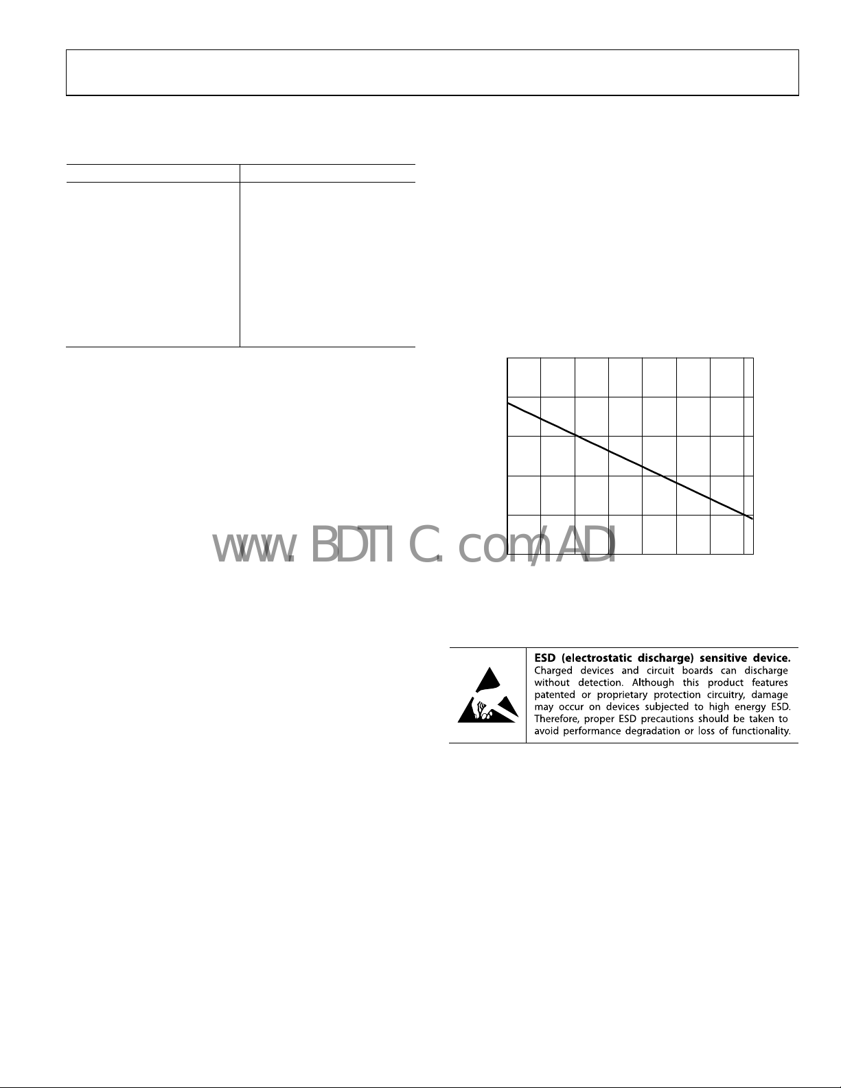
MAXIMUM POWER DISSIPATION
The maximum power that can be safely dissipated by the
ADA4859-3 is limited by the associated rise in junction
temperature. The maximum safe junction temperature
for plastic encapsulated devices is determined by the glass
transition temperature of the plastic, approximately 150°C.
Temporarily exceeding this limit may cause a shift in parametric
performance due to a change in the stresses exerted on the die
by the package. Exceeding a junction temperature of 175°C for
an extended period can result in device failure.
To ensure proper operation, it is necessary to observe the
maximum power derating curves in Figure 2.
2.5
2.0
1.5
1.0
0.5
MAXIMUM POWER DISSIPATION (W)
0
–40 –20 0 20 40 60 80 100
Figure 2. Maximum Power Dissipation vs. Ambient Temperature
AMBIENT TEMP ERATURE (°C)
07715-002
ESD CAUTION
Rev. 0 | Page 5 of 16

ADA4859-3
A
www.BDTIC.com/ADI
PIN CONFIGURATION AND FUNCTION DESCRIPTIONS
DA4859-3
TOP VIEW
(Not to Scale)
–IN1
OUT1
16 15 14 13
+V
1
S
2C1_a
CHARGE
C1_b
CPO
NOTES
1. NC = NO CONNECT .
2. EXPOSED PAD, CONNECT T O GROUND.
PUMP
3
4
5678
S
+V
+IN3
NC
+IN1
12
+IN2
–IN2
11
OUT2
10
PD
9
–IN3
OUT3
07715-003
Figure 3. Pin Configuration
Table 4. Pin Function Descriptions
Pin No. Mnemonic Description
1 +VS Positive Supply for Charge Pump.
2 C1_a Charge Pump Capacitor Side a.
3 C1_b Charge Pump Capacitor Side b.
4 CPO Charge Pump Output.
5 +VS Positive Supply.
6 +IN3 Noninverting Input 3.
7 −IN3 Inverting Input 3.
8 OUT3 Output 3.
9 PD Power Down.
10 OUT2 Output 2.
11 −IN2 Inverting Input 2.
12 +IN2 Noninverting Input 2.
13 NC No Connect.
14 +IN1 Noninverting Input 1.
15 −IN1 Inverting Input 1.
16 OUT1 Output 1.
17 (EPAD) Exposed Pad (EPAD) The exposed pad must be connected to the ground plane.
Rev. 0 | Page 6 of 16

ADA4859-3
www.BDTIC.com/ADI
TYPICAL PERFORMANCE CHARACTERISTICS
VS = 5 V, G = 2, RF = 550 Ω, RL = 150 Ω, large signal V
2
1
0
–1
–2
–3
–4
–5
–6
NORMALIZED CLOSED-LOOP GAIN (dB)
–7
–8
1 10 100 1000
FREQUENCY (MHz)
Figure 4. Small Signal Frequency Response vs. Supply Voltage
0.2
0.1
0
–0.1
–0.2
–0.3
–0.4
–0.5
–0.6
NORMALIZED CLOSED-LOOP GAIN (dB)
–0.7
–0.8
1 10 100 1000
VS = 3.3V
FREQUENCY (MHz)
Figure 5. Large Signal 0.1 dB Flatness vs. Supply Voltage
0
–10
–20
–30
–40
–50
–60
DISTORTION (dBc)
–70
–80
–90
–100
110
FREQUENCY (MHz )
Figure 6. Harmonic Distortion vs. Frequency
HD2
HD3
VS = 3.3V
= 5V
V
S
= 2 V p-p, small signal V
OUT
= 5V
V
S
07715-004
07715-005
100
07715-006
= 0.1 V p-p, and T = 25ºC, unless otherwise noted.
OUT
2
1
0
–1
–2
–3
–4
–5
–6
NORMALIZED CLOSED-LOOP GAIN (dB)
–7
–8
1 10 100 1000
FREQUENCY (MHz)
VS = 3.3V
V
S
Figure 7. Large Signal Frequency Response vs. Supply Voltage
0.2
0.1
0
–0.1
–0.2
–0.3
–0.4
–0.5
NORMALIZED GAIN (dB)
–0.6
–0.7
–0.8
1 10 100 1000
CL = 10pF
CL =14pF
FREQUENCY (MHz )
CL = 10pF
CL = 16pF
Figure 8. Large Signal 0.1 dB Flatness vs. Capacitive Load
0
VS = 3.3V
–10
–20
–30
–40
–50
–60
DISTORTION (dBc)
–70
–80
–90
–100
110
FREQUENCY (MHz )
HD2
HD3
Figure 9. Harmonic Distortion vs. Frequency
= 5V
07715-007
07715-008
100
07715-009
Rev. 0 | Page 7 of 16

ADA4859-3
–
–
www.BDTIC.com/ADI
0
–10
–20
–30
–40
PSRR (dB)
–50
–60
–70
0.1 1 10010 400
FREQUENCY (MHz )
Figure 10. Power Supply Rejection Ratio (PSRR) vs. Frequency
40
07715-010
0.2
0.1
0
–0.1
–0.2
–0.3
–0.4
–0.5
NORMALIZED GAIN (dB)
–0.6
–0.7
VS = 3.3V
–0.8
1 10 100 1000
CL =10pF
CL =14pF
FREQUENCY (MHz )
CL = 16pF
CL =110pF
Figure 13. Large Signal 0.1 dB Flatness vs. Capacitive Load
30
07715-013
–50
–60
–70
–80
FORWARD ISOLATIO N (dB)
–90
–100
0.1 1 10010 400
FREQUENCY (MHz )
Figure 11. Forward Isolation vs. Frequency
250
200
150
100
50
OUTPUT VOLTAGE NOISE (nV/ Hz)
0
100 1k 10k 100k 1M
FREQUENCY (Hz)
Figure 12. Total Output Voltage Noise vs. Frequency
–40
–50
–60
–70
CROSSTALK (dB)
–80
–90
–100
0.1 1 10010 400
07715-011
FREQUENCY (MHz)
07715-014
Figure 14. Crosstalk vs. Frequency
20
18
16
14
12
10
8
6
4
INPUT CURRENT NOI SE (pA/ Hz)
2
0
100 1k 10k 100k 1M
07715-012
FREQUENCY (Hz)
07715-015
Figure 15. Noninverting Input Current Noise vs. Frequency
Rev. 0 | Page 8 of 16

ADA4859-3
www.BDTIC.com/ADI
0.15
0.10
0.05
V
= 200mV p-p
OUT
1.5
CL = 6pFCL = 10pF
1.0
CL = 4pF
0.5
0
–0.05
OUTPUT VO LTAGE (V )
–0.10
–0.15
= 6pF
C
L
TIME (5ns/DIV)
C
L
CL = 4pF
= 10pF
Figure 16. Small Signal Transient Response vs. Capacitive Load
0.15
V
= 200mV p-p
OUT
0.10
0.05
0
–0.05
OUTPUT VOLTAGE (V)
–0.10
–0.15
V
S
VS = 3.3V
TIME (5ns/DIV)
= 5V
Figure 17. Small Signal Transient Response vs. Supply Voltage, CL = 4 pF
1100
1000
900
800
700
600
500
SLEW RATE (V/µ s)
400
300
200
100
00.5 1.51.0 2.52.0
RISE
FALL
OUTPUT VOLTAGE (V p-p)
Figure 18. Slew Rate vs. Output Voltage
0
–0.5
OUTPUT VO LTAGE (V )
–1.0
07715-016
–1.5
TIME (5ns/DIV)
07715-019
Figure 19. Large Signal Transient Response vs. Capacitive Load
1.5
V
= 3.3V
S
1.0
0.5
= 5V (V)
S
0
–0.5
OUTPUT VO LTAGE, V
–1.0
07715-017
–1.5
VS = 5V
TIME (5ns/DIV)
2.0
1.5
1.0
0.5
0
–0.5
–1.0
= 3.3V (V)
S
OUTPUT VOLTAGE, V
07715-020
Figure 20. Large Signal Transient Response vs. Supply Voltage, CL = 4 pF
900
VS = 3.3V
800
700
600
500
400
SLEW RATE (V/µ s)
300
200
100
00.5 1.51.0 2.52.0
07715-018
RISE
FALL
OUTPUT VOLTAGE (V p-p)
07715-021
Figure 21. Slew Rate vs. Output Voltage
Rev. 0 | Page 9 of 16

ADA4859-3
www.BDTIC.com/ADI
5
4
3
2
1
0
OUTPUT VO LTAGE (V )
–1
V
–2
–3
OUT
TIME (20ns/DIV)
V
IN
Figure 22. Output Overdrive Recovery
2.0
1.6
1.2
0.8
0.4
0
–0.4
AMPLITUDE ( V)
–0.8
–1.2
–1.6
–2.0
–5 4035302520151050
TIME (ns)
OUTPUT
INPUT
ERROR
Figure 23. Settling Time (Rise)
0
–0.4
–0.8
–1.2
CHARGE
PUMP CURRENT
2.5
2.0
1.5
1.0
0.5
0
–0.5
–1.0
–1.5
0.5
0.4
0.3
0.2
0.1
0
–0.1
–0.2
–0.3
–0.4
–0.5
24
22
20
18
3.0
VS = 3.3V
2.5
2.0
1.5
1.0
0.5
0
INPUT VOLTAGE (V)
07715-022
–0.5
OUTPUT VO LTAGE (V )
–1.0
–1.5
–2.0
V
OUT
TIME (20ns/DIV)
V
IN
Figure 25. Output Overdrive Recovery
2.0
1.6
1.2
0.8
0.4
0
ERROR (%)
07715-023
–0.4
AMPLITUDE ( V)
–0.8
–1.2
–1.6
–2.0
–5 4035302520151050
TIME (ns)
ERROR
INPUT
OUTPUT
Figure 26. Settling Time, (Fall)
1.5
V
PD
1.0
0.5
V
OUT
1.5
1.0
0.5
0
–0.5
–1.0
0.5
0.4
0.3
0.2
0.1
0
–0.1
–0.2
–0.3
–0.4
–0.5
6
5
4
INPUT VOLTAGE (V)
07715-025
ERROR (%)
07715-026
–1.6
–2.0
–2.4
–2.8
CHARGE PUMP OUTPUT VOLTAGE (V)
–3.2
2.5 5.04.54.03. 53.0
AMPLIFIER
CURRENT
OUTPUT
VOLTAGE
CHARGE PUMP SUPPLY VOLTAGE (V)
16
14
CURRENT (mA)
12
10
8
07715-024
Figure 24. Charge Pump Voltage and Current vs. Supply Voltage
Rev. 0 | Page 10 of 16
0
–0.5
OUTPUT VOLTAGE (V)
–1.0
–1.5
TIME (4 00ns/DIV)
3
2
POWER-DOW N VOLTAG E (V)
1
0
07715-027
Figure 27. Enable/Power-Down Time

ADA4859-3
–
–
www.BDTIC.com/ADI
100
–105
–110
–115
–120
–125
–130
POWER (dBm)
–135
–140
–145
–150
0 0.5 1.0 1.5 2.0 2.5 3. 0 3.5 4.0 4.5 5. 0
CHARGE PUMP HARMONICS
FREQUENCY (MHz )
07715-100
Figure 28. Output Spectrum vs. Frequency
100
–105
–110
–115
–120
–125
–130
POWER (dBm)
–135
–140
–145
–150
0 0.5 1.0 1.5 2.0 2.5 3.0 3.5 4.0 4.5 5.0
CHARGE PUMP HARMONI CS
FREQUENCY (MHz )
V
S
= 3.3V
7715-101
Figure 29. Output Spectrum vs. Frequency
Rev. 0 | Page 11 of 16

ADA4859-3
C
Φ
Φ
www.BDTIC.com/ADI
THEORY OF OPERATION
1
OVERVIEW
The ADA4859-3 is a fixed gain of two, current feedback amplifier
designed for exceptional performance as a triple video amplifier. Its
specifications make it especially suitable for SD and HD video
applications. The ADA4859-3 provides HD video output on a
single supply as low as 3.0 V while only consuming 13 mA per
amplifier. It also features a power-down pin (PD) that reduces
the quiescent current to 4 mA when activated.
The ADA4859-3 can be used in applications that require both
ac- and dc-coupled inputs and outputs. The output stage on the
ADA4859-3 is capable of driving 2 V p-p video signals into two
doubly terminated video loads (150 Ω each) on a single 5 V supply.
The input range of the ADA4859-3 includes ground, whereas
the output range is limited by the output headroom set by the
voltage drop across two diodes from each rail, which occurs
1.2 V from the positive and negative supply rails.
CHARGE PUMP OPERATION
The on-board charge pump creates a negative supply for the
amplifier. It provides different negative voltages depending on
the power supply voltage. For a +5 V supply, the negative supply
generated is equal to −3 V with 150 mA of output supply current,
and for a +3.3 V supply, the negative supply is equal to −2 V
with 45 mA of output supply current.
Figure 30 shows the charging cycle when the supply voltage,
+V
, charges C1 through Φ1 to ground. During this cycle, C1
S
quickly charges to reach the +V
begins with switching Φ
Figure 31. When C1 = C2, the charge in C1 is divided between
the two capacitors and slowly increases the voltage in C2 until it
reaches a predetermined voltage (−3 V for the +5 V supply and
−2 V
for the +3.3 V supply). The typical charge pump charging and
discharging frequency is 550 kHz with a 150 Ω load and no input
signal. This frequency changes with the load current, and it can
get much slower if the amplifier is powered down and no external
current is used.
voltage. The discharge cycle then
S
off and switching Φ2 on, as shown in
1
+V
S
PO
C2
Figure 30. Charging Cycle
+V
S
CPO
C2
Figure 31. Discharging Cycle
The ADA4859-3 specifications make it especially suitable for SD
and HD video applications. It also allows dc-coupled video signal
with its black level set to 0 V and its sync tip down to −300 mV
for YPbPr video.
The charge pump is always on, even when the power-down pin
(PD) is enabled and the amplifier is off. However, it would be in
an idle state if the negative current were not used. Each amplifier
needs −6.3 mA of current, which totals −19 mA for all three
amplifiers. This means additional negative current may be available
by the charge pump for external use. Pin 4 (CPO) is the charge
pump output, which provides access to the negative supply
generated by the charge pump. Placing a 1 μF charge capacitor at
the CPO pin is essential to hold the charge and regulate the ripple.
If the negative supply is used to power another device in the
system, it is only possible for the 5 V supply operation. In the
3.3 V supply operation, the charge pump output current is very
limited. The capacitor at the CPO pin, which regulates the ripple
of the negative voltage, can be used as a coupling capacitor for the
external device. However, the charge pump current should be
limited to a maximum of 50 mA for external use. When powering
down the ADA4859-3, the charge pump is not affected and its
output voltage and current remain available for external use.
a
C1
Φ
b
1
07715-137
2
a
C1
Φ
b
2
07715-138
Rev. 0 | Page 12 of 16

ADA4859-3
V
V
V
V
www.BDTIC.com/ADI
APPLICATIONS INFORMATION
USING THE ADA4859-3 IN GAINS EQUAL TO +1, −1
The ADA4859-3 was designed to offer outstanding video
performance, simplify applications, and minimize board area.
The ADA4859-3 is a triple amplifier with on-chip feedback
and gain set resistors. The gain is fixed internally at G = +2. The
inclusion of the on-chip resistors not only simplifies the design
of the application but also eliminates six surface-mount resistors,
saving valuable board space and lowering assembly costs.
Although the ADA4859-3 has a fixed gain of G = +2, it can be
used in other gain configurations, such as G = −1 and G = +1.
Unity-Gain Operation
Option 1
There are two options for obtaining unity gain (G = +1). The
first is shown in Figure 32. In this configuration, the −IN input
pin is tied to the output. (Feedback is provided through the two
internal 550 Ω resistors in parallel), and the input is applied to
the noninverting input. The noise gain for this configuration is 1.
+
S
10µF
0.1µF
+
S
10µF
0.1µF
R
F
R
G
V
IN
R
T
GAIN OF +1
Figure 33. Unity Gain of Option 2
OUT
07715-131
Inverting Unity-Gain Operation
In this configuration, the noninverting input is tied to ground
and the input signal is applied to the inverting input. The noise
gain for this configuration is +2, see Figure 34.
+
S
10µF
0.01µF
V
IN
R
T
V
OUT
V
V
IN
R
T
GAIN OF +1
OUT
07715-130
Figure 32. Unity Gain of Option 1
Option 2
Another option exists for running the ADA4859-3 as a unitygain amplifier. In this configuration, the noise gain is +2, see
Figure 33. The frequency response and transient response for
this configuration closely match the gain of +2 plots because the
noise gains are equal. This method does have twice the noise
gain of Option 1; however, in applications that do not require low
noise, Option 2 offers less peaking and ringing. By tying the inputs
together, the net gain of the amplifier becomes +1. Equation 1
shows the transfer characteristic for the schematic shown in
Figure 33.
⎛
⎞
−
⎜
=
VV
OUT
IN
⎜
⎝
which simplifies to V
R
R
G
OUT
F
⎟
⎟
⎠
= VIN.
⎛
⎜
+
V
IN
⎜
⎝
⎞
+
RR
F
G
⎟
(1)
⎟
R
G
⎠
GAIN OF –1
07715-132
Figure 34. Inverting Configuration (G = −1)
Figure 35 shows the small signal frequency response for both
gain of +1 (Option 1 and Option 2) and gain of −1 configurations.
It is clear that the G = +1 Option 2 has better flatness and no
peaking compared to Option 1.
3
0
G = +1,
OPTION 2
–3
CLOSED-LOOP GAIN (dB)
–6
VS = 5V
= 2V p-p
V
OUT
= 100Ω
R
L
–9
1 10 100 1000
FREQUENCY (MHz )
Figure 35. Large Signal, G = +1 and G = −1
G = –1
G = +1,
OPTION 1
07715-031
Rev. 0 | Page 13 of 16

ADA4859-3
V
V
www.BDTIC.com/ADI
VIDEO LINE DRIVER
The ADA4859-3 was designed to excel in video driver applications.
Figure 36 shows a typical schematic for a video driver operating
on bipolar supplies.
(R)
(R)
75Ω
1
2
CHARGE
3
4
VIN (B)
16 15 14 13
PUMP
5678
75Ω
V
OUT
1µF
1µF
+
S
+
10µF 0.1µF
Figure 36. Video Driver Schematic
In applications that require multiple video loads be driven
simultaneously, the ADA4859-3 can deliver. Figure 37 shows
the ADA4856-3 configured with two video loads, and Figure 38
shows the large signal performance for multiple video loads.
+V
S
10µF
0.1µF
75Ω
CABLE
V
IN
–
+
75Ω
Figure 37. Video Driver Schematic for Two Video Loads
6.5
6.0
5.5
5.0
4.5
4.0
CLOSED-LOOP GAIN (dB)
3.5
3.0
2.5
1 10 100 1000
Figure 38. Large Signal Frequency Response for Various Loads
FREQUENCY (MHz)
75Ω
75Ω
RL = 75Ω
IN
75Ω
75Ω
12
11
10
9
V
(B)
OUT
75Ω
CABLE
75Ω
CABLE
RL = 150Ω
75Ω
PD
75Ω
VIN (G)
V
OUT
75Ω
75Ω
(G)
V
OUT
V
OUT
07715-034
07715-134
1
2
07715-135
POWER-DOWN
The ADA4859-3 is equipped with a PD (power-down) pin for
all three amplifiers. This allows the user the ability to reduce
the quiescent supply current when an amplifier is not active.
The power-down threshold levels are derived from ground
level. The amplifiers are powered down when the voltage
applied to the PD pin is greater than a certain voltage from
ground. In a 5 V supply application, the voltage is greater than 2 V,
and in a 3.3 V supply application, the voltage is greater than 1.5 V.
The amplifier is enabled whenever the PD pin is left floating
(not connected). If the PD pin is not used, it is best to leave it
floating or connected to ground. Note that the power-down feature
does not control the charge pump output voltage and current.
Table 5. Power-Down Voltage Control
PD Pin 5 V 3.3 V
Not Active <1.5 V <1 V
Active >2 V >1.5 V
LAYOUT CONSIDERATIONS
As is the case with all high speed applications, careful attention
to printed circuit board (PCB) layout details prevents associated
board parasitics from becoming problematic. Proper RF design
technique is mandatory. The PCB should have a ground plane
covering all unused portions of the component side of the board to
provide a low impedance return path. Removing the ground
plane on all layers from the area near the input and output pins
reduces stray capacitance. Locate termination resistors and loads as
close as possible to their respective inputs and outputs. Keep
input and output traces as far apart as possible to minimize
coupling (crosstalk) through the board. Adherence to
microstrip or stripline design techniques for long signal traces
(greater than about 1 inch) is recommended.
POWER SUPPLY BYPASSING
Careful attention must be paid to bypassing the power supply
pins of the ADA4859-3. Use high quality capacitors with low
equivalent series resistance (ESR), such as multilayer ceramic
capacitors (MLCCs), to minimize supply voltage ripple and
power dissipation. A large, usually tantalum, 10 μF to 47 μF
capacitor located in proximity to the ADA4859-3 is required to
provide good decoupling for lower frequency signals. In
addition, locate 0.1 μF MLCC decoupling capacitors as close to
each of the power supply pins as is physically possible, no more
than 1/8-inch away. The ground returns should terminate
immediately into the ground plane. Locating the bypass capacitor
return close to the load return minimizes ground loops and
improves performance.
Rev. 0 | Page 14 of 16

ADA4859-3
www.BDTIC.com/ADI
OUTLINE DIMENSIONS
PIN 1
INDICATOR
1.00
0.85
0.80
12° MAX
SEATING
PLANE
4.00
BSC SQ
TOP
VIEW
0.80 MAX
0.65 TYP
0.35
0.30
0.25
3.75
BSC SQ
0.20 REF
0.60 MAX
0.65 BSC
0.05 MAX
0.02 NOM
COPLANARITY
0.75
0.60
0.50
0.08
0.60 MAX
(BOTTO M VIEW )
16
13
12
9
8
5
1.95 BSC
FOR PROPER CO NNECTION OF
THE EXPOSED PAD, REFER TO
THE PIN CONF IGURATION AND
FUNCTION DES CRIPTIONS
SECTION OF THIS DATA SHEET.
PIN 1
INDICATOR
1
4
5
2
.
2
0
1
.
2
9
.
1
5
0.25 MIN
Q
S
COMPLIANT TO JEDEC STANDARDS MO-220-VGGC
072808-A
Figure 39.16-Lead Lead Frame Chip Scale Package [LFCSP_VQ]
4 mm × 4 mm Body, Very Thin Quad (CP-16-4)
Dimensions shown in millimeters
ORDERING GUIDE
Model Temperature Range Package Description Package Option Ordering Quantity
ADA4859-3ACPZ-R2
ADA4859-3ACPZ-R7
ADA4859-3ACPZ-RL
1
Z = RoHS Compliant Part.
1
–40°C to +105°C 16-Lead LFCSP_VQ CP-16-4 250
1
–40°C to +105°C 16-Lead LFCSP_VQ CP-16-4 1,500
1
–40°C to +105°C 16-Lead LFCSP_VQ CP-16-4 5,000
Rev. 0 | Page 15 of 16

ADA4859-3
www.BDTIC.com/ADI
NOTES
©2008 Analog Devices, Inc. All rights reserved. Trademarks and
registered trademarks are the property of their respective owners.
D07715-0-11/08(0)
Rev. 0 | Page 16 of 16
 Loading...