

V
查询ADA4850-2供应商
High Speed, Rail-to-Rail Output,
FEATURES
Ultralow power-down current: 150 nA/amp max
Low quiescent current: 2.4 mA/amp
High speed
175 MHz −3 dB bandwidth
220 V/µs slew rate
85 ns settling time to 0.1%
Excellent video specifications
0.1 dB flatness: 14 MHz
Differential gain: 0.12%
Differential phase: 0.09°
Single-supply operation: 2.7 V to 6 V
Rail-to-rail output
Output swings to within 80 mV of either rail
Low voltage offset: 0.6 mV
APPLICATIONS
Portable multimedia players
Video cameras
Digital still cameras
Consumer video
Op Amp with Ultralow Power-Down
ADA4850-1/ADA4850-2
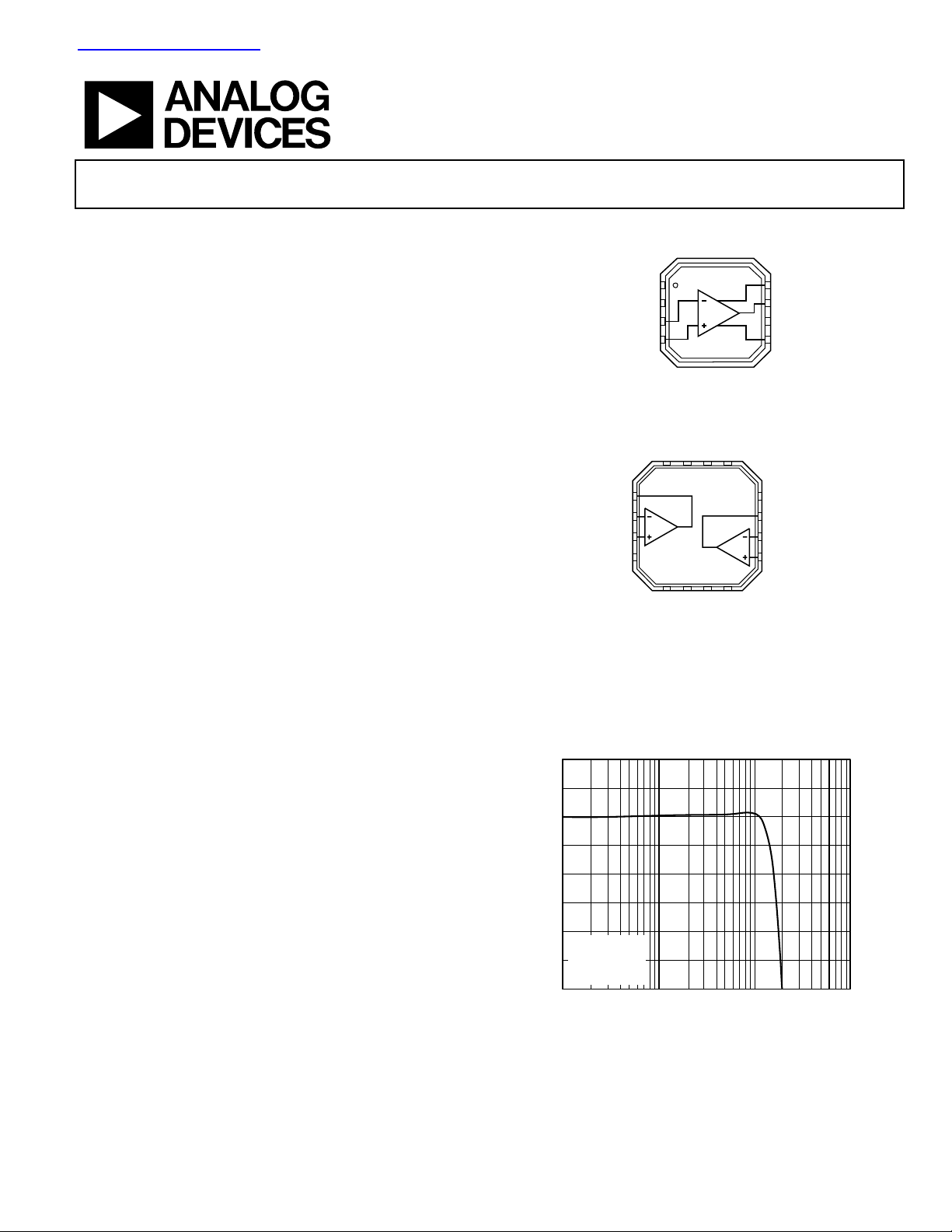
PIN CONFIGURATIONS
ADA4850-1
1POWER DOWN
2NC
–IN
3
4+IN
NC = NO CONNECT
Figure 1. 8-Lead, 3 mm × 3 mm LFCSP
2
1
C
C
D
D
N
6
1
P
N
P
3
4
5
1
1
1
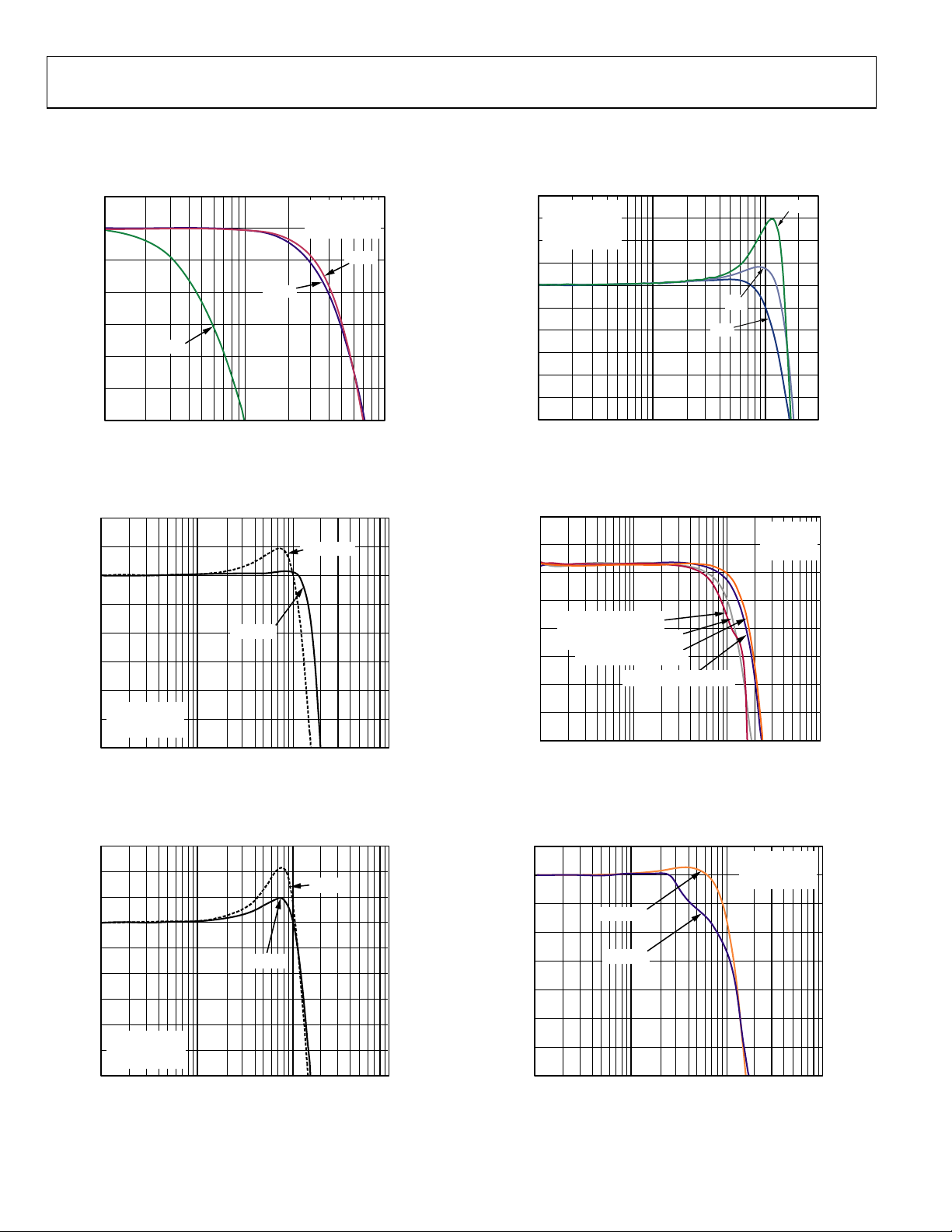
ADA4850-2
1
1
OUT
2–IN1
3+IN1
4–V
S
8
7
5
6
C
C
N
NC = NO CONNECT
C
C
N
N
N
Figure 2. 16-Lead, 3 mm × 3 mm LFCSPP
+V
8
OUTPUT
7
NC
6
–V
5
12 +V
11 V
OUT
10 –IN2
9 +IN2
S
S
05320-106
S
2
05320-043
GENERAL DESCRIPTION
The ADA4850-1, ADA4850-21 are low price, high speed,
voltage feedback rail-to-rail output op amps with ultralow
power-down. Despite their low price, the ADA4850-1/
ADA4850-2 provide excellent overall performance and
versatility. The 175 MHz −3 dB bandwidth and 220 V/µs
slew rate make these amplifiers well-suited for many generalpurpose, high speed applications.
The ADA4850-1/ADA4850-2 are designed to operate at supply
voltages as low as 2.7 V and up to 6 V at 2.4 mA of supply
current per amplifier. In power-down mode, the supply current
is less than 150 nA, ideal for battery-powered applications.
The ADA4850 family provides users with a true single-supply
capability, allowing input signals to extend 200 mV below the
negative rail and to within 2.2 V of the positive rail. The output
of the amplifier can swing within 80 mV of either supply rail.
With its combination of low price, excellent differential gain
(0.12%), differential phase (0.09º), and 0.1 dB flatness out to
14 MHz, these amplifiers are ideal for video applications.
Rev. A
Information furnished by Analog Devices is believed to be accurate and reliable.
However, no responsibility is assumed by Analog Devices for its use, nor for any
infringements of patents or other rights of third parties that may result from its use.
Specifications subject to change without notice. No license is granted by implication
or otherwise under any patent or patent rights of Anal og Devices. Trademarks and
registered trademarks are the property of their respective owners.
The ADA4850-1/ADA4850-2 are designed to work in the
extended temperature range of −40°C to +125°C.
2
1
0
–1
–2
–3
CLOSED-LOOP GAIN (dB)
–4
G = +1
= 5V
V
S
–5
= 1kΩ
R
L
= 0.1V p-p
V
OUT
–6
1 10010 1000
FREQUENCY (MHz)
1
Patent pending.
One Technology Way, P.O. Box 9106, Norwood, MA 02062-9106, U.S.A.
Tel: 781.329.4700
Fax: 781.461.3113 ©2005 Analog Devices, Inc. All rights reserved.
Figure 3. Small Signal Freq uency Respons e
www.analog.com
05320-054

ADA4850-1/ADA4850-2
TABLE OF CONTENTS
Specifications with +3 V Supply..................................................... 3
Headroom and Overdrive Recovery Considerations ............ 12
Specifications with +5 V Supply..................................................... 4
Absolute Maximum Ratings ............................................................ 5
Thermal Resistance ...................................................................... 5
ESD Caution.................................................................................. 5
Typical Performance Characteristics ............................................. 6
Circuit Description......................................................................... 12
REVISION HISTORY
4/05—Rev. 0 to Rev. A
AddedADA4850-1..............................................................Universal
Added 8-Lead LFCSP.........................................................Universal
Changes to Features.......................................................................... 1
Changes to General Description .................................................... 1
Changes to Figure 3.......................................................................... 1
Changes to Table 1............................................................................ 3
Changes to Table 2............................................................................ 4
Changes to Power-Down Pins Section and Table 5 ................... 13
Updated Outline Dimensions....................................................... 14
Changes to Ordering Guide.......................................................... 14
Operating the ADA4850-1/ADA4850-2 on
Bipolar Supplies
Power-Down Pins....................................................................... 13
Outline Dimensions ....................................................................... 14
Ordering Guide .......................................................................... 14
.......................................................................... 13
2/05—Revision 0: Initial Version
Rev. A | Page 2 of 16

ADA4850-1/ADA4850-2
SPECIFICATIONS WITH +3 V SUPPLY
TA = 25°C, RF = 0 Ω for G = +1, RF = 1 kΩ for G > +1, RL = 1 kΩ, unless otherwise noted.
Table 1.
Parameter Conditions Min Typ Max Unit
DYNAMIC PERFORMANCE
−3 dB Bandwidth G = +1, VO = 0.1 V p-p 160 MHz
G = +2, VO = 0.5 V p-p, RL = 150 Ω 45 MHz
Bandwidth for 0.1 dB Flatness G = +2, VO = 0.5 V p-p, RL = 150 Ω 14 MHz
Slew Rate G = +2, VO = 1 V Step 110 V/µs
Settling Time to 0.1% G = +2, VO = 1 V Step, RL = 150 Ω 80 ns
NOISE/DISTORTION PERFORMANCE
Harmonic Distortion (dBc) HD2/HD3 fC = 1 MHz, VO = 2 V p-p, G = +3, RL = 150 Ω −72/−77 dBc
Input Voltage Noise f = 100 kHz 10
Input Current Noise f = 100 kHz 2.5
Differential Gain G = +3, NTSC, RL = 150 Ω, VO = 2 V p-p 0.2 %
Differential Phase G = +3, NTSC, RL = 150 Ω, VO = 2 V p-p 0.2 Degrees
DC PERFORMANCE
Input Offset Voltage 0.6 4.1 mV
Input Offset Voltage Drift 4
Input Bias Current 2.4 4.4 µA
Input Bias Current Drift 4
Input Bias Offset Current 30 nA
Open-Loop Gain VO = 0.25 V to 0.75 V 78 100 dB
INPUT CHARACTERISTICS
Input Resistance Differential/common-mode 0.5/5.0 MΩ
Input Capacitance 1.2 pF
Input Common-Mode Voltage Range −0.2 to +0.8 V
Input Overdrive Recovery Time (Rise/Fall) VIN = +3.5 V to −0.5 V, G = +1 60/50 ns
Common-Mode Rejection Ratio VCM = 0.5 V −76 −108 dB
POWER-DOWN
Power-Down Input Voltage Power-down ADA4850-1/ADA4850-2 <0.7/<0.6 V
Enabled ADA4850-1/ADA4850-2 >0.8/>1.7 V
Turn-Off Time 0.7 µs
Turn-On Time 60 ns
Power-Down Bias Current/ Power Down Pin
Enabled Power-down = 3 V 37 55 µA
Power-Down Power-down = 0 V 0.01 0.2 µA
OUTPUT CHARACTERISTICS
Output Overdrive Recovery Time (Rise/Fall) VIN = +0.7 V to −0.1 V, G = +5 70/100 ns
Output Voltage Swing 0.06 to 2.83 0.03 to 2.92 V
Short-Circuit Current Sinking/sourcing 105/74 mA
POWER SUPPLY
Operating Range
1
2.7 6 V
Quiescent Current/Amplifier 2.4 2.8 mA
Quiescent Current (Power-Down)/Amplifier 15 150 nA
Positive Power Supply Rejection +VS = +3 V to +4 V, −VS = 0 V −83 −100 dB
Negative Power Supply Rejection +VS = +3 V, −VS = 0 V to –1 V −83 −102 dB
1
For operation on bipolar supplies, see the section. Operating the ADA4850-1/ADA4850-2 on Bipolar Supplies
nV/√Hz
pA/√Hz
µV/°C
nA/°C
Rev. A | Page 3 of 16

ADA4850-1/ADA4850-2
SPECIFICATIONS WITH +5 V SUPPLY
TA = 25°C, RF = 0 Ω for G = +1, RF = 1 kΩ for G > +1, RL = 1 kΩ, unless otherwise noted.
Table 2.
Parameter Conditions Min Typ Max Unit
DYNAMIC PERFORMANCE
−3 dB Bandwidth G = +1, VO = 0.1 V p-p 175 MHz
G = +1, VO = 0.5 V p-p 110 MHz
Bandwidth for 0.1 dB Flatness G = +2, VO = 1.4 V p-p, RL = 150 Ω 9 MHz
Slew Rate G = +2, VO = 4 V Step 220 V/µs
G = +2, VO = 2 V Step 160 V/µs
Settling Time to 0.1% G = +2, VO = 1 V Step, RL = 150 Ω 85 ns
NOISE/DISTORTION PERFORMANCE
Harmonic Distortion (dBc) HD2/HD3 fC = 1 MHz, VO = 2 V p-p, G = +2, RL = 150 Ω −81/−86 dBc
Input Voltage Noise f = 100 kHz 10
Input Current Noise f = 100 kHz 2.5
Differential Gain G = +3, NTSC, RL = 150 Ω 0.12 %
Differential Phase G = +3, NTSC, RL = 150 Ω 0.09 Degrees
Crosstalk(RTI)-ADA4850-2 f = 4.5 MHz, RL = 150 Ω, VO = 2 V p-p 60 dB
DC PERFORMANCE
Input Offset Voltage 0.6 4.2 mV
Input Offset Voltage Drift 4
Input Bias Current 2.3 4.2 µA
Input Bias Current Drift 4
Input Bias Offset Current 30 nA
Open-Loop Gain VO = 2.25 V to 2.75 V 83 105 dB
INPUT CHARACTERISTICS
Input Resistance Differential/common-mode 0.5/5.0 MΩ
Input Capacitance 1.2 pF
Input Common-Mode Voltage Range −0.2 to +2.8 V
Input Overdrive Recovery Time (Rise/Fall) VIN = +5.5 V to −0.5 V, G = +1 50/40 ns
Common-Mode Rejection Ratio VCM = 2.0 V −85 −110 dB
POWER-DOWN
Power-Down Input Voltage Power-down ADA4850-1/ADA4850-2 <0.7/<0.6 V
Enabled ADA4850-1/ADA4850-2 >0.8/>1.7 V
Turn-Off Time 0.7 µs
Turn-On Time 50 ns
Power-Down Bias Current/ Power Down Pin
Enabled Power-down = 5 V 0.05 0.13 mA
Power-Down Power-down = 0 V 0.02 0.2 µA
OUTPUT CHARACTERISTICS
Output Overdrive Recovery Time (Rise/Fall) VIN = +1.1 V to −0.1 V, G = +5 60/70 ns
Output Voltage Swing 0.14 to 4.83 0.07 to 4.92 V
Short-Circuit Current Sinking/sourcing 118/94 mA
POWER SUPPLY
Operating Range
1
2.7 6 V
Quiescent Current/Amplifier 2.5 2.9 mA
Quiescent Current (Power-Down)/Amplifier 15 150 nA
Positive Power Supply Rejection +VS = +5 V to +6 V, −VS = 0 V −84 −100 dB
Negative Power Supply Rejection +VS = +5 V, −VS = −0 V to −1 V −84 −102 dB
1
For operation on bipolar supplies, see the section. Operating the ADA4850-1/ADA4850-2 on Bipolar Supplies
nV/√Hz
pA/√Hz
µV/°C
nA/°C
Rev. A | Page 4 of 16

ADA4850-1/ADA4850-2
(
ABSOLUTE MAXIMUM RATINGS
Table 3.
Parameter Rating
Supply Voltage 12.6 V
Power Dissipation See Figure 4
Power Down Pin Voltage (−VS + 6) V
Common-Mode Input Voltage (−VS − 0.5 ) V to (+VS + 0.5) V
Differential Input Voltage +VS to −V
S
Storage Temperature −65°C to +125°C
Operating Temperature Range −40°C to +125°C
Lead Temperature Range
300°C
(Soldering 10 sec)
Junction Temperature 150°C
Stresses above those listed under Absolute Maximum Ratings
may cause permanent damage to the device. This is a stress
rating only; functional operation of the device at these or any
other conditions above those indicated in the operational
section of this specification is not implied. Exposure to absolute
maximum rating conditions for extended periods may affect
device reliability.
The power dissipated in the package (P
quiescent power dissipation and the power dissipated in the die
due to the ADA4850-1/ADA4850-2 drive at the output. The
quiescent power is the voltage between the supply pins (V
times the quiescent current (I
= Quiescent Power + (Total D riv e P o w er − Load Power)
P
D
⎛
V
()
D
⎜
IVP
SS
⎜
2
⎝
).
S
⎞
V
OUTS
⎟
×+×=
⎟
R
L
⎠
RMS output voltages should be considered. If R
, as in single-supply operation, the total drive power is
to −V
S
V
× I
. If the rms signal levels are indeterminate, consider
S
OUT
the worst case, when V
()
D
IVP
SS
= VS/4 for RL to midsupply.
OUT
2
)
4V
/
S
+×=
R
L
In single-supply operation with R
case is V
= VS/2.
OUT
) is the sum of the
D
)
S
2
V
OUT
–
R
L
is referenced
L
referenced to −VS, the worst
L
THERMAL RESISTANCE
θJA is specified for the worst-case conditions, that is, θJA is
specified for the device soldered in the circuit board for surfacemount packages.
Table 4. Thermal Resistance
Package Type θ
JA
16-Lead LFCSP 91 °C/W
8-Lead LFCSP 80 °C/W
Unit
Airflow increases heat dissipation, effectively reducing θ
Also, more metal directly in contact with the package leads and
exposed paddle from metal traces, through holes, ground, and
power planes reduce θ
.
JA
Figure 4 shows the maximum safe power dissipation in the
package vs. the ambient temperature for the LFCSP (91°C/W)
package on a JEDEC standard 4-layer board. θ
approximations.
2.5
Maximum Power Dissipation
The maximum safe power dissipation for the ADA4850-1/
ADA4850-2 is limited by the associated rise in junction
temperature (T
) on the die. At approximately 150°C, which is
J
the glass transition temperature, the plastic changes its
2.0
1.5
LFCSP-8
LFCSP-16
properties. Even temporarily exceeding this temperature limit
may change the stresses that the package exerts on the die,
1.0
permanently shifting the parametric performance of the
ADA4850-1/ADA4850-2. Exceeding a junction temperature of
150°C for an extended period of time can result in changes in
0.5
MAXIMUM POWER DISSIPATION (W)
silicon devices, potentially causing degradation or loss of
functionality.
0
–55 125–45–35–25–15–5 5 152535455565758595105115
AMBIENT TEMPERATURE (°C)
Figure 4. Maximum Power Dissipation vs. Temperature for a 4-Layer Board
ESD CAUTION
ESD (electrostatic discharge) sensitive device. Electrostatic charges as high as 4000 V readily accumulate
on the human body and test equipment and can discharge without detection. Although this product features
proprietary ESD protection circuitry, permanent damage may occur on devices subjected to high energy
electrostatic discharges. Therefore, proper ESD precautions are recommended to avoid performance
degradation or loss of functionality.
values are
JA
.
JA
05320-055
Rev. A | Page 5 of 16
ADA4850-1/ADA4850-2
TYPICAL PERFORMANCE CHARACTERISTICS
TA = 25°C, RF = 0 Ω for G = +1, RF = 1 kΩ for G > +1, RL = 1 kΩ, unless otherwise noted.
1
0
–1
–2
–3
–4
–5
NORMALIZED CLOSED-LOOP GAIN (dB)
–6
1 10 100
G = +10
FREQUENCY (MHz)
G = +2
VS = 5V
R
= 150Ω
L
V
OUT
= 0.1V p-p
Figure 5. Small Signal Frequency Response for Various Gains
2
1
0
–1
–2
–3
CLOSED-LOOP GAIN (dB)
–4
VS = 5V
G = +1
–5
V
= 0.1V p-p
OUT
–6
1 10010 1000
RL = 1kΩ
FREQUENCY (MHz)
RL = 150Ω
Figure 6. Small Signal Frequency Response for Various Loads
3
2
1
0
–1
–2
–3
CLOSED-LOOP GAIN (dB)
–4
G = +1
R
= 150Ω
–5
L
= 0.1V p-p
V
OUT
–6
1 10010 1000
FREQUENCY (MHz)
VS = 5V
= 3V
V
S
Figure 7. Small Signal Frequency Response for Various Supplies
G = –1
05320-044
05320-045
05320-046
4
G = +1
= 5V
V
3
S
= 1kΩ
R
L
V
2
OUT
1
0
–1
–2
–3
CLOSED-LOOP GAIN (dB)
–4
–5
–6
1 10010 300
Figure 8. Small Signal Frequency Response for Various Capacitor Loads
6.2
6.1
6.0
5.9
V
5.8
GAIN (dB)
5.7
5.6
5.5
5.4
100k 100M
1
0
–1
–2
–3
–4
CLOSED-LOOP GAIN (dB)
–5
–6
–7
1 10010 1000
Figure 10. Large Frequency Response for Various Loads
= 0.1V p-p
FREQUENCY (MHz)
= 5V, V
S
VS = 5V, V
OUT
VS = 3V, V
= 2V p-p
= 1.4V p-p
OUT
= 0.5V p-p
OUT
VS = 5V, V
1M 10M
= 0.1V p-p
OUT
FREQUENCY (Hz)
Figure 9. 0.1 dB Flatness Response
R
= 150Ω
L
= 1kΩ
R
L
FREQUENCY (MHz)
0pF
1pF
VS = 5V
G = +2
R
VS = 5V
G = +1
V
OUT
6pF
= 150Ω
L
= 0.5V p-p
05320-007
05320-047
05320-048
Rev. A | Page 6 of 16

ADA4850-1/ADA4850-2
3
VS = 3V
G = +1
2
= 1kΩ
R
L
= 0.1V p-p
V
OUT
1
0
–1
–2
CLOSED-LOOP GAIN (dB)
–3
–4
+25°C
–40°C
+125°C
+85°C
300
G = +2
= 5V
V
S
= 1kΩ
R
L
250
200
150
100
SLEW RATE (V/µs)
50
NEGATIVE SLEW RATE
POSITIVE SLEW RATE
–5
1 1000
10 100
FREQUENCY (MHz)
Figure 11. Small Signal Frequency Response for Various Temperatures
3
VS = 5V
G = +1
2
= 1kΩ
R
L
= 0.1V p-p
V
OUT
1
0
–1
–2
CLOSED-LOOP GAIN (dB)
–3
–4
–5
1 1000
+25°C
–40°C
10 100
FREQUENCY (MHz)
+125°C
+85°C
Figure 12. Small Signal Frequency Response for Various Temperatures
140
120
100
80
60
PHASE
VS = 5V
0
–30
–60
–90
–120
05320-057
05320-098
0
0 0.5 1.0 1.5 2.0 2.5 3.0 3.5 4.0 4.5
OUTPUT VOLTAGE STEP (V)
Figure 14. Slew Rate vs. Output Voltage
10k
1k
A)
µ
VS = 3V, 5V, ADA4850-2
100
10
SUPPLY CURRENT (
VS = 3V, 5V, ADA4850-1 ENABLE
VS = 3V, 5V, ADA4850-1 POWER DOWN
1
0.1
0.5 1.0 1.5 2.0 2.5 3.0 3.5 4.0 4.5
0 5.0
POWER-DOWN VOLTAGE (V)
Figure 15. Supply Current vs. Power-Down Voltage
–40
G = +2
= 5V
V
S
= 150Ω
R
L
–50
–60
–70
V
OUT
V
OUT
= 2V p-p
2 TO V
OUT
1
5.0
05320-024
05320-036
40
OPEN-LOOP GAIN (dB)
20
0
–20
GAIN
100k10k100 1k10 1M 10M 100M 1G
FREQUENCY (Hz)
Figure 13. Open-Loop Gain and Phase vs. Frequency
–150
–180
–210
–240
OPEN-LOOP PHASE (Degrees)
05320-012
–80
CROSSTALK (dB)
–90
–100
V
1 TO V
OUT
1M100k 10M 100M
FREQUENCY (Hz)
OUT
2
Figure 16. Cross talk vs. Frequen cy
05320-037
Rev. A | Page 7 of 16

ADA4850-1/ADA4850-2
–
–
40
G = +1
= 5V
V
S
–50
= 500mV p-p
V
OUT
2.575
2.550
G = +1
= 5V
V
S
R
= 150Ω
L
10pF
0pF
–60
= 1kΩ HD2
R
–70
–80
–90
HARMONIC DISTORTION (dBc)
–100
–110
0.1 100
L
RL = 150Ω HD2
R
= 1kΩ HD3
L
R
= 150Ω HD3
L
110
FREQUENCY (MHz)
Figure 17. Harmonic Distortion vs. Frequency for Various Loads
50
G = +2
= 5V
V
S
= 1kΩ
R
L
–60
–70
V
OUT
–80
–90
–100
HARMONIC DISTORTION (dBc)
–110
–120
0.1 100
V
= 200mV p-p
HD2
= 500mV p-p
OUT
HD2
V
= 200mV p-p
OUT
HD3
V
= 500mV p-p
OUT
HD3
110
FREQUENCY (MHz)
Figure 18. Harmonic Distortion vs. Frequency for Various V
0.65
G = +2
R
= 1kΩ
L
= 5V
V
S
0.60
OUT
05320-102
05320-103
2.525
2.500
2.475
OUTPUT VOLTAGE (V)
2.450
2.425
0 20 40 60 80 100 120 140 160 180 200
TIME (ns)
Figure 20. Small Signal Transient Response for Capacitive Load
3.25
G = +2
= 1kΩ
R
L
= 5V
V
S
3.00
2.75
2.50
2.25
2.00
OUTPUT VOLTAGE FOR 5V SUPPLY (V)
1.75
500 100 150 200
TIME (ns)
Figure 21. Large Signal Transient Response
2.875
G = +1
R
= 1kΩ
L
2.750
0.875
0.750
05320-020
05320-050
0.55
0.50
0.45
OUTPUT VOLTAGE (V)
0.40
0.35
500 100 150 200
TIME (ns)
Figure 19. Small Signal Transient Response for Various Supplies
05320-019
2.625
2.500
OUTPUT VOLTAGE FOR 5V SUPPLY (V)
2.375
2.250
2.125
V
= 3V
S
500 100 150 200
TIME (ns)
VS = 5V
Figure 22. Large Signal Transient Response for Various Supplies
0.625
0.500
0.375
0.250
0.125
OUTPUT VOLTAGE FOR 3V SUPPLY (V)
05320-049
Rev. A | Page 8 of 16

ADA4850-1/ADA4850-2
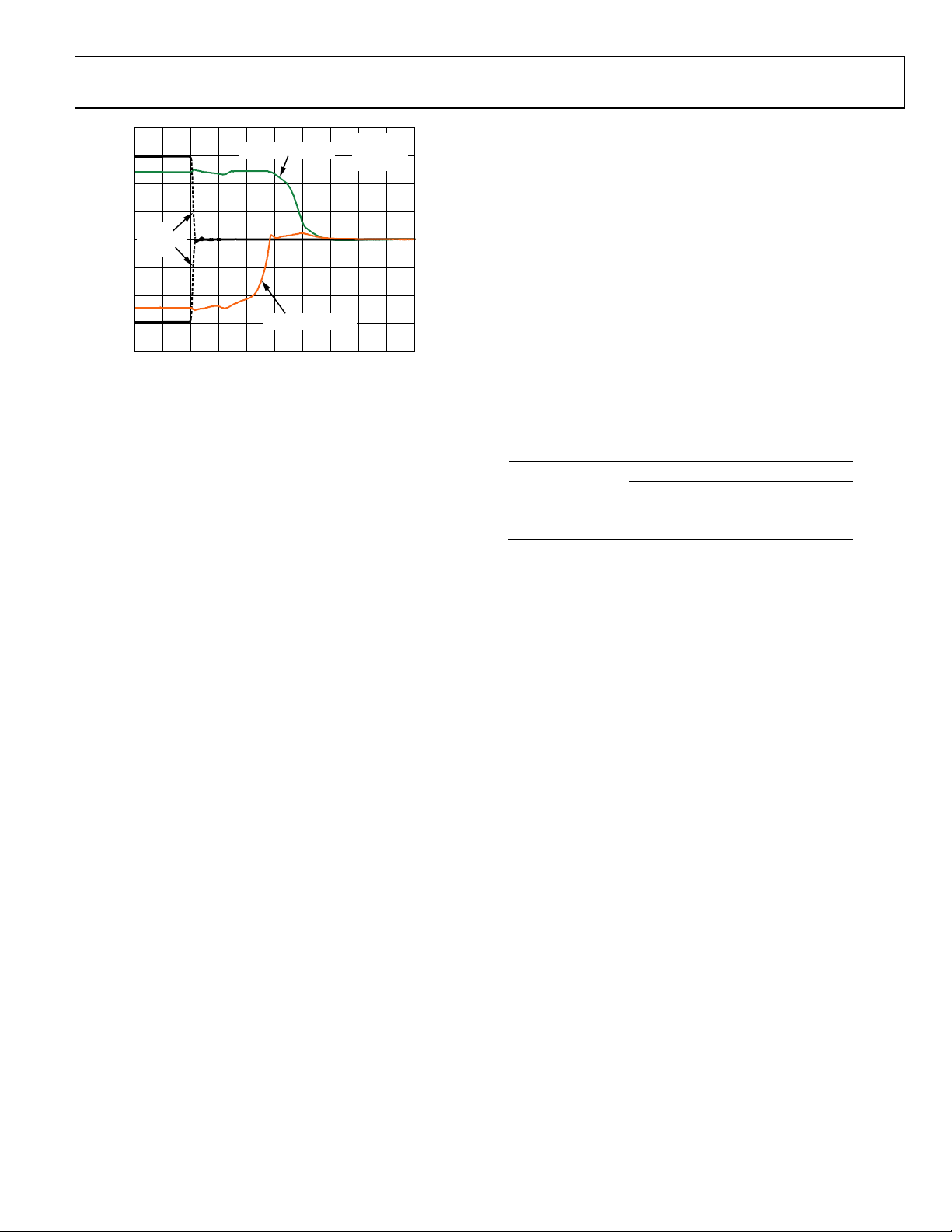
6
5
V
4
DISABLE
3
2
VOLTAGE (V)
1
0
–1
03015 45
V
OUT
TIME (µs)
Figure 23. Enable/Disable Time
5.5
5.0
4.5
4.0
3.5
3.0
2.5
2.0
1.5
1.0
INPUT AND OUTPUT VOLTAGE (V)
0.5
0
–0.5
0 1000
OUTPUT
100 200 300 400 500 600 700 800 900
INPUT
TIME (ns)
Figure 24. Input Overdrive Recovery
3.5
3.0
2.5
2.0
1.5
1.0
0.5
INPUT AND OUTPUT VOLTAGE (V)
0
5 × INPUT
OUTPUT
G = +2
VS = 5V
f
= 400kHz
IN
G = +1
V
= 5V
S
R
= 150Ω
L
f = 1MHz
G = +5
V
= 3V
S
R
= 150Ω
L
f = 1MHz
05320-025
05320-058
1000
100
10
VOLTAGE NOISE (nV/ Hz)
100
10
CURRENT NOISE (pA/ Hz)
350
300
250
200
COUNT
150
100
50
1
1
100k10k100 1k10 1M 10M 100M
FREQUENCY (Hz)
Figure 26. Voltage Noise vs. Frequency
100k10k100 1k10 1M 10M 100M 1G
FREQUENCY (Hz)
Figure 27. Current Noise vs. Frequency
VS = 5V
N = 1720
x = 450µV
σ = 750µV
05320-059
05320-095
–0.5
100 200 300 400 500 600 700 800 900
0 1000
TIME (ns)
Figure 25. Output Overdrive Recovery
05320-060
Rev. A | Page 9 of 16
0
–4 4
–3–2–10123
V
(mV)
OFFSET
Figure 28. Input Offset Voltage Distribution
05320-065
ADA4850-1/ADA4850-2
400
380
360
340
320
V)
µ
(
300
OS
V
280
260
240
220
200
–1.0 3.5
Figure 29. Input Offset Voltage vs. Common-Mode Voltage
0.6
0.5
0.4
VS = 5V
–0.5 0 0.5 1.0 1.5 2.0 2.5 3.0
VCM (V)
+V
SAT
VS = 3V
05320-063
–1.2
+I
B
–1.4
–1.6
VS = 5V
–1.8
–2.0
INPUT BIAS CURRENT (µA)
–2.2
–2.4
–25–105 203550658095110
–40 125
TEMPERATURE (°C)
VS = 3V
–I
B
Figure 32. Input Bias Current vs. Temperature for Various Supplies
95
VS = 5V
= 1kΩ
R
L
90
+VS– V
85
OUT
05320-092
0.3
0.2
0.1
OUTPUT SATURATION VOLTAGE (V)
0
050
5 1015202530354045
LOAD CURRENT (mA)
VS = 5V
–V
SAT
05320-064
Figure 30. Output Saturation Voltage vs. Load Current
(Voltage Differential from Rails)
–30
–32
A)
µ
–34
–36
–38
–40
–42
–44
POWER-DOWN PIN BIAS CURRENT (
–46
–25–105 203550658095110
–40 125
VS = 3V
VS = 5V
TEMPERATURE (°C)
05320-091
Figure 31. Power-Down Bias Current vs. Temperature for Various Supplies
80
75
70
OUTPUT SATURATION VOLTAGE (mV)
65
–40 125
–25 –10 5 20 35 50 65 80 95 110
Figure 33. Output Saturation Voltage vs. Temperature
4.9
4.8
4.7
4.6
4.5
4.4
SUPPLY CURRENT (mA)
4.3
4.2
–25–105 203550658095110
–40 125
Figure 34. Current vs. Temperature for Various Supplies
–VS– V
OUT
TEMPERATURE (°C)
(Voltage Differential from Rails)
VS = 5V
VS = 3V
TEMPERATURE (°C)
05320-062
05320-090
Rev. A | Page 10 of 16

ADA4850-1/ADA4850-2
0
VS = 5V
–10
–20
–30
–40
–50
–60
–70
–80
–90
POWER SUPPLY REJECTION (dB)
–100
–110
100
+PSR
1M100k1k 10k 10M 100M
FREQUENCY (Hz)
Figure 35. Power Supply Rejection (PSR) vs. Frequency
0.7
0.6
–PSR
05320-094
–20
VS = 5V
–30
–40
–50
–60
–70
–80
–90
–100
COMMON-MODE REJECTION (dB)
–110
–120
1k
10k 100k 1M 10M 100M
CHANNEL 1
CHANNEL 2
FREQUENCY (Hz)
Figure 37. Common-Mode Rejection Ratio (CMRR) vs. Frequency
05320-034
0.5
0.4
0.3
0.2
0.1
INPUT OFFSET VOLTAGE (mV)
0
–0.1
–40 125
–25–105 203550658095110
VS = 5V
VS = 3V
TEMPERATURE (°C)
Figure 36. Input Offset Voltage vs. Temperature for Various Supplies
05320-093
Rev. A | Page 11 of 16
ADA4850-1/ADA4850-2
CIRCUIT DESCRIPTION
The ADA4850-1/ADA4850-2 feature a high slew rate input
stage that is a true single-supply topology, capable of sensing
signals at or below the negative supply rail. The rail-to-rail
output stage can swing to within 80 mV of either supply rail
when driving light loads and within 0.17 V when driving 150 Ω.
High speed performance is maintained at supply voltages as low
as 2.7 V.
HEADROOM AND OVERDRIVE RECOVERY
CONSIDERATIONS
Input
The ADA4850-1/ADA4850-2 are designed for use in low
voltage systems. To obtain optimum performance, it is useful to
understand the behavior of the amplifier as input and output
signals approach the amplifier’s headroom limits. The input
common-mode voltage range extends 200 mV below the
negative supply voltage or ground for single-supply operation to
within 2.2 V of the positive supply voltage. Therefore, in a gain
of +3, the ADA4850-1/ADA4850-2 can provide full rail-to-rail
output swing for supply voltage as low as 3.3 V, assuming the
input signal swing is from −V
Exceeding the headroom limit is not a concern for any inverting
gain on any supply voltage, as long as the reference voltage at
the amplifier’s positive input lies within the amplifier’s input
common-mode range.
The input stage sets the headroom limit for signals when the
amplifier is used in a gain of +1 for signals approaching the
positive rail. For high speed signals, however, there are other
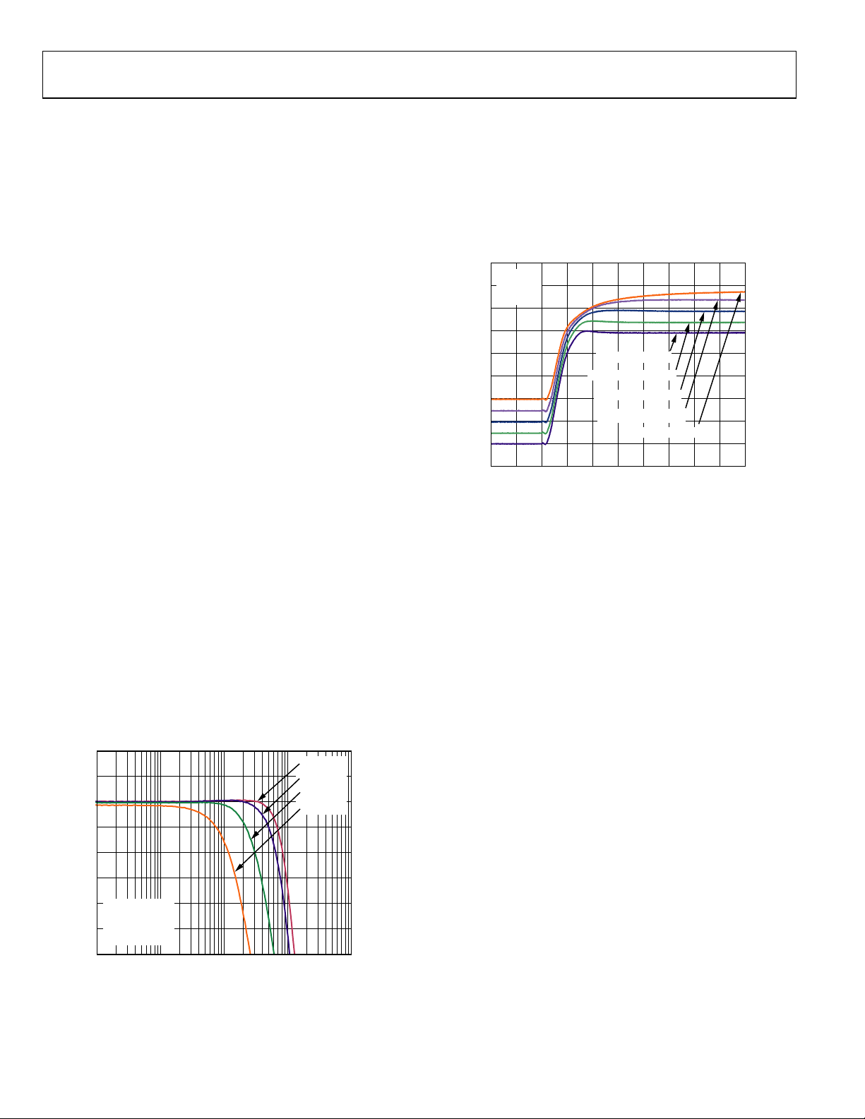
considerations. Figure 38 shows −3 dB bandwidth vs. dc input
voltage for a unity-gain follower. As the common-mode voltage
approaches the positive supply, the bandwidth begins to drop
when within 2 V of +V
distortion or settling time.
2
1
0
–1
–2
GAIN (dB)
–3
–4
VS = 5V
G = +1
R
= 1kΩ
L
–5
V
= 0.1V p-p
OUT
–6
0.1 1000
1 10 100
Figure 38. Unity-Gain Follower Bandwidth vs.
Frequency for Various Input Common-Mode
(or ground) to 1.1 V.
S
. This can manifest itself in increased
S
VCM = 3V
V
= 3.1V
CM
V
= 3.2V
CM
V
= 3.3V
CM
FREQUENCY (MHz)
05320-096
Higher frequency signals require more headroom than the
lower frequencies to maintain distortion performance. Figure 39
illustrates how the rising edge settling time for the amplifier
configured as a unity-gain follower stretches out as the top of a
1 V step input approaches and exceeds the specified input
common-mode voltage limit.
3.6
VS = 5V
3.4
G = +1
R
= 1kΩ
L
3.2
3.0
2.8
2.6
2.4
OUTPUT VOLTAGE (V)
2.2
2.0
1.8
0 100
10 20 30 40 50 60 70 80 90
V
STEP
V
STEP
V
STEP
V
TIME (ns)
STEP
= 2V TO 3V
= 2.1V TO 3.1V
= 2.2V TO 3.2V
= 2.3V TO 3.3V
V
= 2.4V TO 3.4V
STEP
05320-061
Figure 39. Pulse Response, Input Headroom Limits
The recovery time from input voltages 2.2 V or closer to the
positive supply is approximately 50 ns, which is limited by the
settling artifacts caused by transistors in the input stage coming
out of saturation.
The ADA4850-1/ADA4850-2 do not exhibit phase reversal, even
for input voltages beyond the voltage supply rails. Going more than
0.6 V beyond the power supplies turns on protection diodes at the
input stage, which greatly increase the current draw of the devices.
Output
For signals approaching the negative supply and inverting gain,
and high positive gain configurations, the headroom limit is the
output stage. The ADA4850-1/ADA4850-2 amplifiers use a
common-emitter output stage. This output stage maximizes the
available output range, limited by the saturation voltage of the
output transistors. The saturation voltage increases with drive
current, due to the output transistor collector resistance.
As the saturation point of the output stage is approached, the
output signal shows increasing amounts of compression and
clipping. As in the input headroom case, higher frequency signals
require a bit more headroom than the lower frequency signals.
Output overload recovery is typically within 40 ns after the
amplifier’s input is brought to a nonoverloading value.
Figure 40 shows the output recovery transients for the amplifier
recovering from a saturated output from the top and bottom
supplies to a point at midsupply.
Rev. A | Page 12 of 16
ADA4850-1/ADA4850-2
6.5
= +2.5V TO 0V
V
5.5
4.5
3.5
INPUT
2.5
VOLTAGE
EDGES
1.5
0.5
INPUT AND OUTPUT VOLTAGE (V)
–0.5
–1.5
0 100
10 20 30 40 50 60 70 80 90
OUT
V
OUT
TIME (ns)
= –2.5V TO 0V
Figure 40. Overload Recovery
VS = 5V
G = –1
R
= 1kΩ
L
05320-042
OPERATING THE ADA4850-1/ADA4850-2 ON
BIPOLAR SUPPLIES
The ADA4850-1/ADA4850-2 can operate on bipolar supplies
up to ±5 V. The only restriction is that the voltage between −V
S
and the power-down pin must not exceed 6 V. Voltage
differences greater than 6 V can cause permanent damage to the
amplifier. For example, when operating on ±5 V supplies, the
power-down pin must not exceed +1 V.
POWER-DOWN PINS
The ADA4850-1/ADA4850-2 feature an ultralow power-down
mode that lowers the supply current to less than 150 nA. When
a power-down pin is brought to within 0.6 V of the negative
supply, the amplifier is powered down. Table 5 outlines the
power-down pin functionality. To ensure proper operation, the
power-down pins (PD) should not be left floating.
Table 5. Power-Down Pins Functionality
3 V and 5 V
Supply Voltage ADA4850-1 ADA4850-2
Powered Down 0 V to 0.7 V 0 V to 0.6 V
Enabled 0.8 to +V
S
1.7 V to +V
S
Rev. A | Page 13 of 16

ADA4850-1/ADA4850-2
R
R
R
OUTLINE DIMENSIONS
PIN 1
INDICATO
3.00
BSC SQ
TOP
VIEW
2.75
BSC SQ
0.45
0.50
BSC
0.60 MAX
8
5
EXPOSED
PAD
(BOTTOM VIEW)
0.50
0.40
0.30
4
PIN 1
INDICATOR
1
1.89
1.50
1.74
REF
1.59
0.90
0.85
0.80
SEATING
PLANE
INDICATO
12° MAX
PIN 1
0.90
0.85
0.80
SEATING
PLANE
0.25
0.80 MAX
MIN
0.65 TYP
0.05 MAX
0.02 NOM
0.30
0.23
0.20 REF
0.18
Figure 41. 8-Lead Lead Frame Chip Scale Package [LFCSP_VD]
3 mm × 3 mm Body, Very Thin, Dual Lead
(CP-8-2)
Dimensions shown in millimeters
12° MAX
3.00
BSC SQ
TOP
VIEW
0.30
0.23
0.18
*
COMPLIANT
EXCEPT FOR EXPOSED PAD DIMENSION.
2.75
BSC SQ
0.80 MAX
0.65 TYP
0.05 MAX
0.02 NOM
0.20 REF
TO
JEDEC STANDARDS MO-220-VEED-2
0.45
0.50
BSC
1.50 REF
0.60 MAX
13
12
EXPOSED
PAD
(BOTTOM VIEW)
9
8
Figure 42. 16-Lead Lead Frame Chip Scale Package [LFCSP_VQ]
3 mm × 3 mm Body, Very Thin Quad
(CP-16-3)
Dimensions shown in millimeters
1.60
1.45
1.30
0.50
0.40
0.30
16
1
4
5
N
P
I
D
N
I
*
1.65
1.50 SQ
1.35
0.25 MIN
1
O
A
C
T
I
ORDERING GUIDE
Model Temperature Range Package Description Package Outline Branding
ADA4850-1YCPZ-R2
ADA4850-1YCPZ-RL1 −40°C to +125°C 8-Lead Lead Frame Chip Scale Package (LFCSP_VD) CP-8-2 HWB
ADA4850-1YCPZ-RL71 −40°C to +125°C 8-Lead Lead Frame Chip Scale Package (LFCSP_VD) CP-8-2 HWB
ADA4850-2YCPZ-R21 −40°C to +125°C 16-Lead Lead Frame Chip Scale Package (LFCSP_VQ) CP-16-3 HTB
ADA4850-2YCPZ-RL1 −40°C to +125°C 16-Lead Lead Frame Chip Scale Package (LFCSP_VQ) CP-16-3 HTB
ADA4850-2YCPZ-RL71 −40°C to +125°C 16-Lead Lead Frame Chip Scale Package (LFCSP_VQ) CP-16-3 HTB
1
Z = Pb-free part.
1
−40°C to +125°C 8-Lead Lead Frame Chip Scale Package (LFCSP_VD) CP-8-2 HWB
Rev. A | Page 14 of 16

ADA4850-1/ADA4850-2
NOTES
Rev. A | Page 15 of 16

ADA4850-1/ADA4850-2
NOTES
©2005 Analog Devices, Inc. All rights reserved. Trademarks and
registered trademarks are the property of their respective owners.
D05320–0−4/05(A)
Rev. A | Page 16 of 16

 Loading...