

Page 1
A
–
查询ADA4841-1供应商
Low Power, Low Noise and Distortion,
FEATURES
Low power: 1.1 mA/amp
Low wideband noise
2.1 nV/√Hz
1.4 pA/√Hz
Low 1/f noise
7 nV/√Hz @ 10 Hz
13 pA/√Hz @ 10 Hz
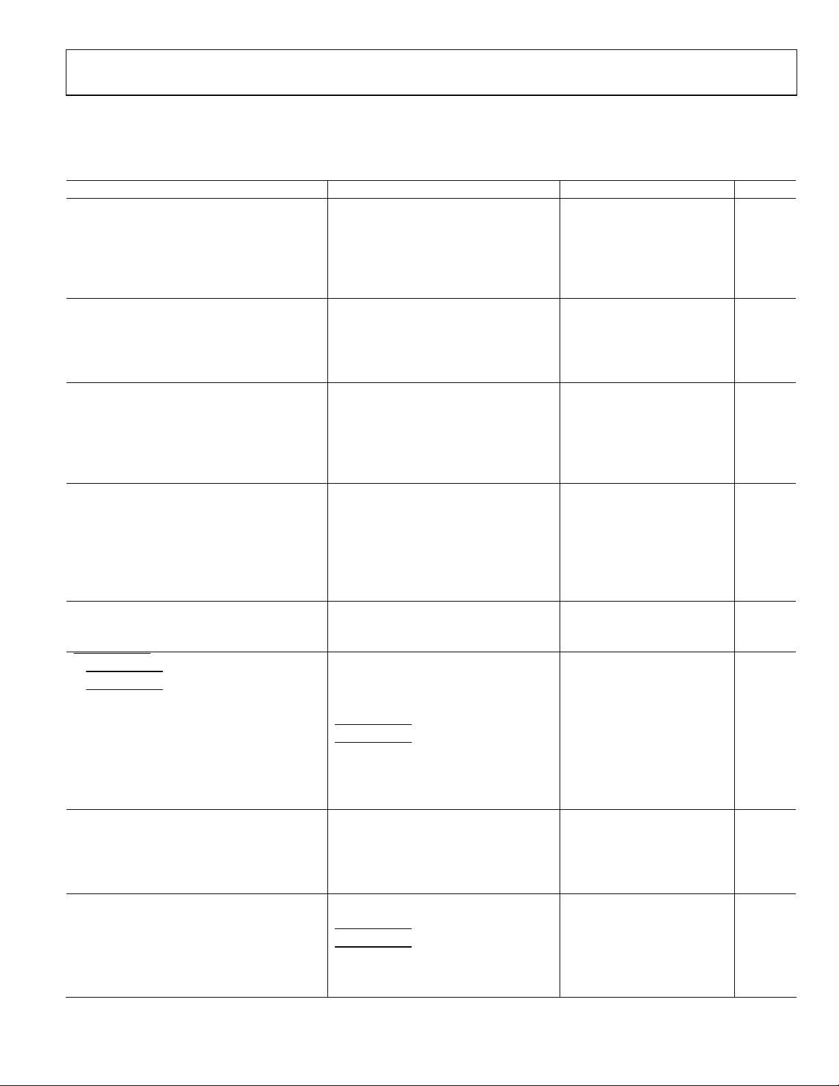
Low distortion: −105 dBc @ 100 kHz, V
High speed
80 MHz, −3 dB bandwidth (G = +1)
12 V/μs slew rate
175 ns settling time to 0.1%
Low offset voltage 0.3 mV max
Rail-to-rail output
Power down
Wide supply range: 2.7 V to 12 V
APPLICATIONS
Low power, low noise signal processing
Battery-powered instrumentation
16-bit PulSAR® ADC drivers
GENERAL DESCRIPTION
= 2 V p-p
O
Rail-to-Rail Output Amplifier
ADA4841-1/ADA4841-2
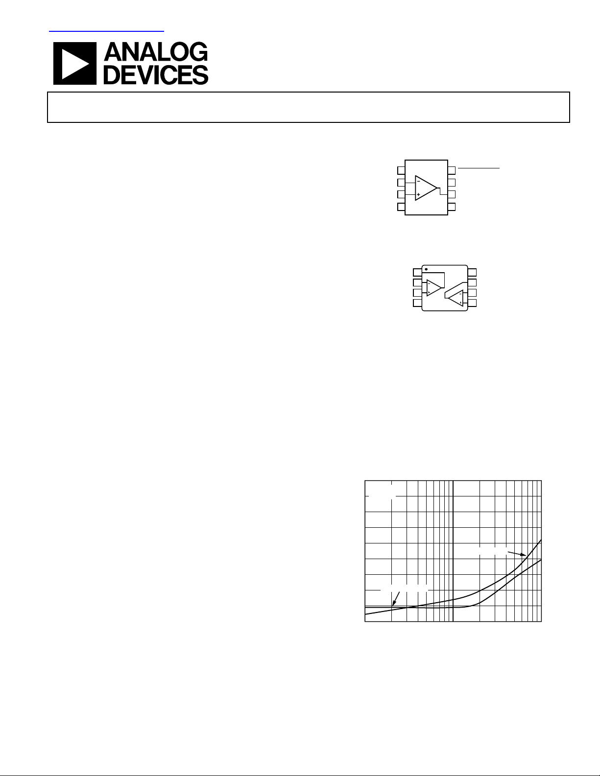
CONNECTION DIAGRAMS
DA4841-1
TOP VIEW
NC
18
(Not to Scale)
–IN
27
+IN
3
–V
4
S
Figure 1. 8-Lead SOIC (R)
ADA4841-2
1
OUT1
2
–IN1
+IN1
3
–V
4
S
(Not to Scale)
Figure 2. 8-Lead MSOP (RM-8)
6
5
TOP VIEW
POWER DOWN
+V
S
V
OUT
NC
8
+V
S
7
OUT2
–IN2
6
+IN2
5
5614-064
05614-001
The ADA4841-1/ADA4841-2 are unity gain stable, low
noise and distortion, rail-to-rail output amplifiers that have a
quiescent current of 1.5 mA maximum. Despite their low power
consumption, these amplifiers offer low wideband voltage noise
performance of 2.1 nV/√Hz and 1.4 pA/√Hz current noise,
along with excellent spurious-free dynamic range (SFDR) of
−105 dBc at 100 kHz. To maintain a low noise environment at
lower frequencies, the amplifiers have low 1/f noise of 7 nV/√Hz
and 13 pA/√Hz at 10 Hz.
The ADA4841-1/ADA4841-2 output can swing to less than
100 mV of either rail. The input common-mode voltage range
extends down to the negative supply. The ADA4841-1/
ADA4841-2 can drive up to 20 pF of capacitive load with
minimal peaking.
The ADA4841-1/ADA4841-2 provide the performance required
to efficiently support emerging 16-bit to 18-bit ADCs and are
ideal for portable instrumentation, high channel count, industrial
measurement, and medical applications. The ADA4841-1/
ADA4841-2 are ideally suited to drive the
AD7685/AD7686,
16-bit PulSAR ADCs.
Rev. B
Information furnished by Analog Devices is believed to be accurate and reliable. However, no
responsibility is assumed by Anal og Devices for its use, nor for any infringements of patents or ot her
rights of third parties that may result from its use. Specifications subject to change without notice. No
license is granted by implication or otherwise under any patent or patent rights of Analog Devices.
Trademarks and registered trademarks are the property of their respective owners.
The ADA4841-1/ADA4841-2 packages feature Pb-free lead
finish. The amplifiers are rated to work over the industrial
temperature range (−40°C to +125°C).
30
VS = ±5V
G = +1
–40
–50
–60
–70
–80
–90
HARMONIC DIS TORTION (dBc)
–100
–110
–120
2V p-p SECOND
0.01 1
FREQUENCY (MHz)
Figure 3. Harmonic Distortion
One Technology Way, P.O. Box 9106, Norwood, MA 02062-9106, U.S.A.
Tel: 781.329.4700 www.analog.com
Fax: 781.461.3113 © 2005 Analog Devices, Inc. All rights reserved.
2V p-p THIRD
0.1
05614-048
Page 2

ADA4841-1/ADA4841-2
TABLE OF CONTENTS
Features .............................................................................................. 1
Headroom Considerations........................................................ 14
Applications....................................................................................... 1
Connection Diagrams...................................................................... 1
General Description......................................................................... 1
Revision History ............................................................................... 2
Specifications..................................................................................... 3
Absolute Maximum Ratings............................................................ 6
Thermal Resistance ...................................................................... 6
ESD Caution.................................................................................. 6
Typical Performance Characteristics............................................. 7
Theory of Operation ...................................................................... 13
Amplifier Description................................................................ 13
DC Errors.................................................................................... 13
Noise Considerations................................................................. 13
REVISION HISTORY
Capacitance Drive...................................................................... 15
Input Protection ......................................................................... 15
Power-Down Operation ............................................................ 16
Applications..................................................................................... 17
Typical Performance Values...................................................... 17
16-Bit ADC Driver..................................................................... 17
Reconstruction Filter................................................................. 17
Layout Considerations............................................................... 18
Ground Plane.............................................................................. 18
Power Supply Bypassing............................................................ 18
Outline Dimensions .......................................................................19
Ordering Guide .......................................................................... 20
10/05—Rev. A to Rev. B
Added ADA4841-2.............................................................Universal
Changes to General Description and Features ............................. 1
Changes to Table 1............................................................................ 3
Changes to Table 2............................................................................ 4
Changes to Table 3............................................................................ 5
Changes to Table 4, Table 5, and Figure 4..................................... 6
Changes to Figure 6.......................................................................... 7
Changes to Figure 12, Figure 13, Figure 15, and Figure 16......... 8
Deleted Figure 25; Renumber Sequentially................................. 10
Changes to Figure 24 and Figure 28............................................. 10
Changes to Figure 31...................................................................... 11
Inserted Figure 37; Renumber Sequentially................................ 12
Changes to Amplifier Description Section and Figure 39........ 13
Changed DC Performance Considerations Section
to DC Errors Section...................................................................... 13
Changes to Noise Considerations Section .................................. 14
Changes to Headroom Considerations Section and Figure 39 15
Changes to Power-Down Operation Section.............................. 16
Changes to 16-Bit ADC Driver Section,
Figure 48, and Figure 49................................................................ 17
Changes to Power Supply Bypassing Section.............................. 18
Updated Outline Dimensions....................................................... 19
Changes to Ordering Guide.......................................................... 20
9/05—Rev. 0 to Rev. A
Changes to Features..........................................................................1
Changes to Figure 2...........................................................................1
Changes to Figure 12.........................................................................8
Changes to Figure 40...................................................................... 14
Changes to Headroom Considerations Section ......................... 15
7/05—Revision 0: Initial Version
Rev. B | Page 2 of 20
Page 3
ADA4841-1/ADA4841-2
SPECIFICATIONS
TA = 25°C, VS = ±5 V, RL = 1 kΩ, Gain = +1, unless otherwise noted.
Table 1.
Parameter Conditions Min Typ Max Unit
DYNAMIC PERFORMANCE
−3 dB Bandwidth VO = 0.02 V p-p 58 80 MHz
V
Slew Rate G = +1, VO = 9 V step, RL = 1 kΩ 12 13 V/μs
Settling Time to 0.1% G = +1, VO = 8 V step 650 ns
Settling Time to 0.01% G = +1, VO = 8 V step 1000 ns
NOISE/HARMONIC PERFORMANCE
Harmonic Distortion HD2/HD3 fC = 100 kHz, VO = 2 V p-p, G = +1 −111/−105 dBc
f
Input Voltage Noise f = 100 kHz 2.1 nV/√Hz
Input Current Noise f = 100 kHz 1.4 pA/√Hz
DC PERFORMANCE
Input Offset Voltage 40 300 μV
Input Offset Voltage Drift 1 μV/°C
Input Bias Current 3 5.3 μA
Input Offset Current 0.1 0.4 μA
Open-Loop Gain VO = ±4 V 103 120 dB
INPUT CHARACTERISTICS
Input Resistance, Common Mode 90 MΩ
Input Resistance, Differential Mode 25 kΩ
Input Capacitance, Common Mode 1 pF
Input Capacitance, Differential Mode 3 pF
Input Common-Mode Voltage Range −5.1 +4 V
Common-Mode Rejection Ratio (CMRR) VCM = −2 V to +2 V 95 115 dB
MATCHING CHARACTERISTICS (ADA4841-2)
Input Offset Voltage 70 μV
Input Bias Current 60 nA
POWER DOWN PIN (ADA4841-1)
POWER DOWN Voltage
POWER DOWN Voltage
Input Current
Enable
Power Down
Switching Speed
Enable 1 μs
Power Down 40 μs
OUTPUT CHARACTERISTICS
Output Voltage Swing G > +1 ±4.90 ±4.955 V
Output Current Limit Sourcing, VIN = +VS , RL = 50 Ω to GND 30 mA
Sinking, VIN = −VS , RL = 50 Ω to GND 60 mA
Capacitive Load Drive 30% overshoot 15 pF
POWER SUPPLY
Operating Range 2.7 12 V
Quiescent Current/Amplifier
Positive Power Supply Rejection Ratio +VS = +5 V to +6 V, −VS = −5 V 95 110 dB
Negative Power Supply Rejection Ratio +VS = +5 V, −VS = −5 V to +6 V 96 120 dB
= 2 V p-p 3 MHz
O
= 1 MHz, VO = 2 V p-p −80/−67 dBc
C
Enabled >3.6 V
Power down <3.2 V
POWER DOWN = +5 V
POWER DOWN = −5 V
POWER DOWN = +5 V
POWER DOWN = −5 V
1 2 μA
−13 −30 μA
1.2 1.5 mA
40 90 μA
Rev. B | Page 3 of 20
Page 4
ADA4841-1/ADA4841-2
TA = 25°C, VS = 5 V, RL = 1 kΩ, Gain = +1, VCM = 2.5 V, unless otherwise noted.
Table 2.
Parameter Conditions Min Typ Max Unit
DYNAMIC PERFORMANCE
−3 dB Bandwidth VO = 0.02 V p-p 54 80 MHz
V
Slew Rate G = +1, VO = 4 V step, RL = 1 kΩ 10 12 V/μs
Settling Time to 0.1% G = +1, VO = 2 V step 175 ns
Settling Time to 0.01% G = +1, VO = 2 V step 550 ns
NOISE/HARMONIC PERFORMANCE
Harmonic Distortion HD2/HD3 fC = 100 kHz, VO = 2 V p-p −109/−105 dBc
f
Input Voltage Noise f = 100 kHz 2.1 nV/√Hz
Input Current Noise f = 100 kHz 1.4 pA/√Hz
Crosstalk f = 100 kHz −117 dB
DC PERFORMANCE
Input Offset Voltage 40 300 μV
Input Offset Voltage Drift 1 μV/°C
Input Bias Current 3 5.3 μA
Input Offset Current 0.1 0.4 μA
Open-Loop Gain VO = 0.5 V to 4.5 V 103 124 dB
INPUT CHARACTERISTICS
Input Resistance, Common Mode 90 MΩ
Input Resistance, Differential Mode 25 kΩ
Input Capacitance, Common Mode 1 pF
Input Capacitance, Differential Mode 3 pF
Input Common-Mode Voltage Range −0.1 +4 V
Common-Mode Rejection Ratio (CMRR) VCM = 2.5 V to 4 V 88 115 dB
MATCHING CHARACTERISTICS (ADA4841-2)
Input Offset Voltage 70 μV
Input Bias Current 70 nA
POWER DOWN PIN (ADA4841-1)
POWER DOWN Voltage
POWER DOWN Voltage
Input Current
Enable
Power Down
Switching Speed
Enable 1 μs
Power Down 40 μs
OUTPUT CHARACTERISTICS
Output Voltage Swing G > +1 0.065 to 4.920 0.029 to 4.974 V
Output Current Limit Sourcing, VIN = +VS, RL = 50 Ω to V
Sinking, VIN = −VS, RL = 50 Ω to V
Capacitive Load Drive 30% overshoot 15 pF
POWER SUPPLY
Operating Range 2.7 12 V
Quiescent Current/Amplifier
Positive Power Supply Rejection Ratio +VS = +5 V to +6 V, −VS = 0 V 95 110 dB
Negative Power Supply Rejection Ratio +VS = +5 V, −VS = 0 V to −1 V 96 120 dB
= 2 V p-p 3 MHz
O
= 1 MHz, VO = 2 V p-p −78/−66 dBc
C
Enabled >3.6
Power down <3.2 V
POWER DOWN = 5 V
POWER DOWN = 0 V
CM
POWER DOWN = 5 V
POWER DOWN = 0 V
1 2 μA
−13 −30 μA
30 mA
CM
60 mA
1.1 1.4 mA
35 70 μA
Rev. B | Page 4 of 20
Page 5
ADA4841-1/ADA4841-2
TA = 25°C, VS = 3 V, RL = 1 kΩ, Gain =+1, VCM = 1.5 V, unless otherwise noted.
Table 3.
Parameter Conditions Min Typ Max Unit
DYNAMIC PERFORMANCE
−3 dB Bandwidth VO = 0.02 V p-p 52 80 MHz
Slew Rate G = +1, VO = 2 V step, RL = 1 kΩ 10 12 V/μs
Settling Time to 0.1% G = +1, VO = 1 V step 120 ns
Settling Time to 0.01% G = +1, VO = 1 V step 250 ns
NOISE/HARMONIC PERFORMANCE
Harmonic Distortion HD2/HD3 fC = 100 kHz, VO = 1 V p-p −97/−100 dBc
f
Input Voltage Noise f = 100 kHz 2.1 nV/√Hz
Input Current Noise f = 100 kHz 1.4 pA/√Hz
DC PERFORMANCE
Input Offset Voltage 40 300 μV
Input Offset Voltage Drift 1 μV/°C
Input Bias Current 3 5.3 μA
Input Offset Current 0.1 0.4 μA
Open-Loop Gain VO = 0.5 V to 2.5 V 101 123 dB
INPUT CHARACTERISTICS
Input Resistance, Common Mode 90 MΩ
Input Resistance, Differential Mode 25 kΩ
Input Capacitance, Common Mode 1 pF
Input Capacitance, Differential Mode 3 pF
Input Common-Mode Voltage Range −0.1 +2 V
Common-Mode Rejection Ratio (CMRR) VCM = 1.5 V to 1.9 V 86 115 dB
MATCHING CHARACTERISTICS (ADA4841-2)
Input Offset Voltage 70 μV
Input Bias Current 60 nA
POWER DOWN PIN (ADA4841-1)
POWER DOWN Voltage
POWER DOWN Voltage
Input Current
Enable
Power Down
Switching Speed
Enable 1 μs
Power Down 40 μs
OUTPUT CHARACTERISTICS
Output Voltage Swing G > +1 0.045 to 2.955 0.023 to 2.988 V
Output Current Limit Sourcing, VIN = +VS, RL = 50 Ω to V
Sinking, VIN = −VS, RL = 50 Ω to V
Capacitive Load Drive 30% overshoot 30 pF
POWER SUPPLY
Operating Range 2.7 12 V
Quiescent Current/Amplifier
Positive Power Supply Rejection Ratio +VS = +3 V to +4 V, −VS = 0 V 95 110 dB
Negative Power Supply Rejection Ratio +VS = +3 V, −VS = 0 V to −1 V 96 120 dB
= 1 MHz, VO = 1 V p-p −79/−80 dBc
C
Enabled >1.6
Power down <1.2 V
POWER DOWN = 3 V
POWER DOWN = 0 V
CM
POWER DOWN = 3 V
POWER DOWN = 0 V
1 2 μA
−10 −30 μA
30 mA
CM
60 mA
1.1 1.3 mA
25 60 μA
Rev. B | Page 5 of 20
Page 6
ADA4841-1/ADA4841-2
(
)
ABSOLUTE MAXIMUM RATINGS
Table 4.
Parameter Rating
Supply Voltage 12.6 V
Power Dissipation See Figure 4
Common-Mode Input Voltage −VS − 0.5 V to +VS + 0.5 V
Differential Input Voltage
±1.8 V
Storage Temperature Range −65°C to +125°C
Operating Temperature Range −40°C to +85°C
Lead Temperature JEDEC J-STD-20
Junction Temperature 150°C
The power dissipated in the package (P
quiescent power dissipation and the power dissipated in the die
due to the amplifier’s drive at the output. The quiescent power is
the voltage between the supply pins (V
current (I
).
S
= Quiescent Power + (Total Dr i v e Po w e r − Load Power)
P
D
⎛
V
V
OUTS
()
D
⎜
IVP
SS
×+×=
⎜
R
2
⎝
L
) is the sum of the
D
) times the quiescent
S
2
⎞
V
OUT
⎟
-
⎟
⎠
R
L
Stresses above those listed under Absolute Maximum Ratings
may cause permanent damage to the device. This is a stress
rating only; functional operation of the device at these or any
other conditions above those indicated in the operational
section of this specification is not implied. Exposure to absolute
maximum rating conditions for extended periods may affect
device reliability.
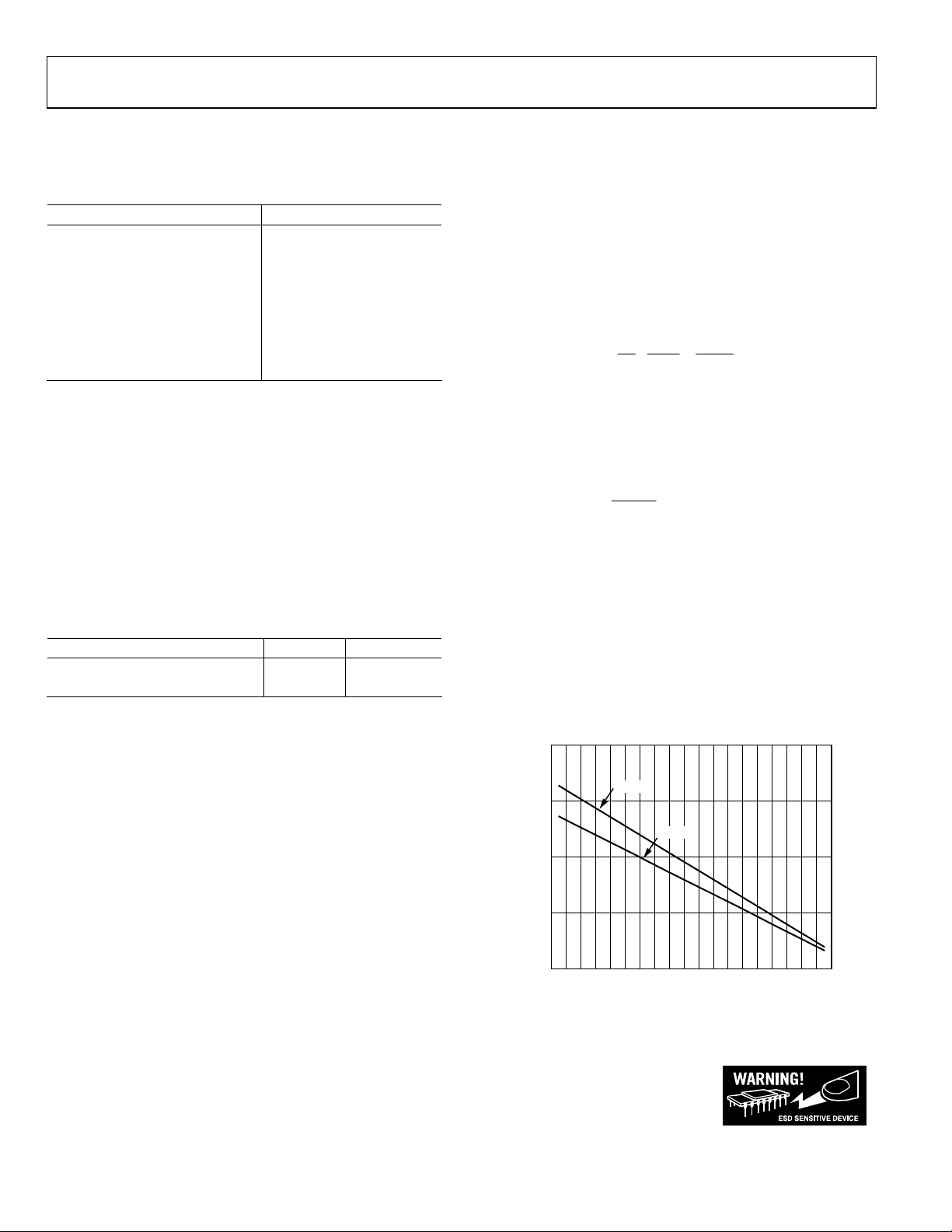
THERMAL RESISTANCE
θJA is specified for the worst-case conditions, that is, θJA is
specified for device soldered in circuit board for surface-mount
packages.
Table 5. Thermal Resistance
Package Type θ
JA
8-lead SOIC 125 °C/W
8-lead MSOP 130 °C/W
Maximum Power Dissipation
The maximum safe power dissipation for the ADA4841-1/
ADA4841-2 is limited by the associated rise in junction
temperature (T
) on the die. At approximately 150°C, which is
J
the glass transition temperature, the plastic changes its
properties. Even temporarily exceeding this temperature limit
may change the stresses that the package exerts on the die,
permanently shifting the parametric performance of the
amplifiers. Exceeding a junction temperature of 150°C for an
extended period can result in changes in silicon devices,
potentially causing degradation or loss of functionality.
Unit
RMS output voltages should be considered. If RL is referenced
, as in single-supply operation, the total drive power is
to −V
S
V
× I
. If the rms signal levels are indeterminate, consider the
S
OUT
worst case, when V
()
D
In single-supply operation with R
= VS/2.
is V
OUT
Airflow increases heat dissipation, effectively reducing θ
= VS/4 for RL to midsupply.
OUT
2
4/
V
S
+×=
IVP
SS
R
L
referenced to −VS, worst case
L
.
JA
In addition, more metal directly in contact with the package
leads and through holes under the device reduces θ
.
JA
Figure 4 shows the maximum safe power dissipation in the
package vs. the ambient temperature for the 8-lead MSOP
(145°C/W) and the 8-lead SOIC (125°C/W) on a JEDEC
standard 4-layer board. θ
2.0
1.5
1.0
0.5
MAXIMUM POWER DISSIPATION (W)
values are approximations.
JA
SOIC
MSOP
0
–35 –15 5 25 45 65 85 105 125
–55
AMBIENT TEMPERATURE (°C)
Figure 4. Maximum Power Dissipation vs. Temperature for a 4-Layer Board
05614-061
ESD CAUTION
ESD (electrostatic discharge) sensitive device. Electrostatic charges as high as 4000 V readily accumulate on
the human body and test equipment and can discharge without detection. Although this product features
proprietary ESD protection circuitry, permanent damage may occur on devices subjected to high energy
electrostatic discharges. Therefore, proper ESD precautions are recommended to avoid performance
degradation or loss of functionality.
Rev. B | Page 6 of 20
Page 7
ADA4841-1/ADA4841-2
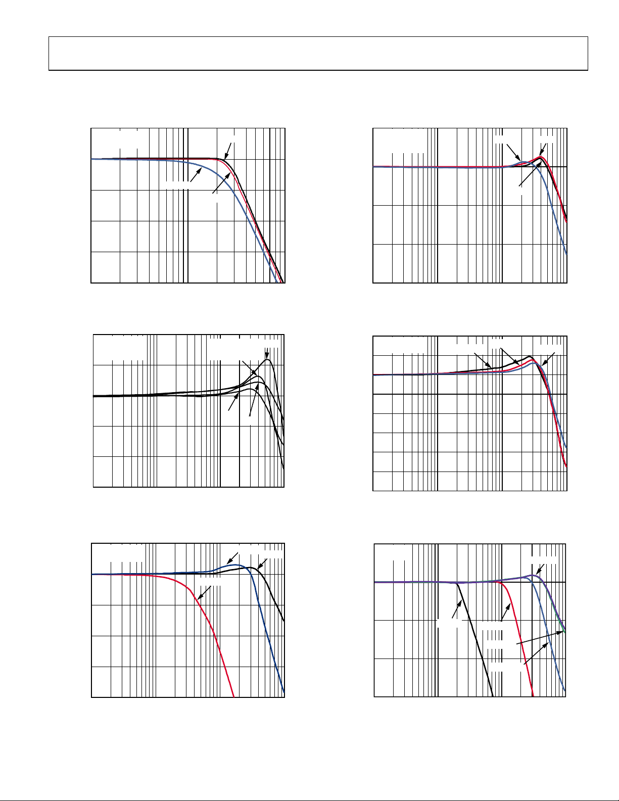
TYPICAL PERFORMANCE CHARACTERISTICS
RL = 1 kΩ, unless otherwise noted.
3
V
= 2V pp
OUT
V
= 5V
S
0
–3
–6
–9
NORMALIZED CLOSED-LOOP GAIN (dB)
–12
0.1 10
G = +10
1
FREQUENCY (MHz)
G = +1
G = +2
Figure 5. Large Signal Frequency Response vs. Gain
6
3
0
–3
CLOSED-LOOP GAIN (dB)
–6
–9
VIN = 20mV p-p
G = +1
V
= 5V
S
0.1
110
FREQUENC Y (MHz)
20pF
WITH
100Ω SNUBBER
0pF
10pF
Figure 6. Small Signal Frequency Response vs. Capacitive Load
20pF
100
05614-021
05614-026
3
VS = 5V
V
= 20mV p-p
IN
G = +1
0
–3
GAIN (dB)
–6
–9
0.1 100
110
FREQUENCY (MHz)
–40°C
+125°C
Figure 8. Small Signal Frequency Response vs. Temperature
2
VIN = 20mV p-p
G = +1
1
0
–1
–2
GAIN (dB)
–3
–4
–5
–6
0.1 100
VS = +3V
110
FREQUENCY (MHz)
VS = +5V
Figure 9. Small Signal Frequency Response vs. Supply Voltage
+25°C
05614-028
VS = ±5V
05614-029
3
VIN = 20mV p-p
V
= 5V
S
0
–3
–6
–9
NORMALIZED CLOSED-LOOP GAIN (dB)
–12
0.1 100
110
FREQUENCY (MHz)
G = +10
G = –1
Figure 7. Small Signal Frequency Response vs. Gain
G = +1
05614-027
Rev. B | Page 7 of 20
3
VS = ±5V
G = +1
0
–3
GAIN (dB)
–6
–9
0.1
2V p-p
110
FREQUENCY (MHz)
400mV p-p
20mV p-p
100mV p-p
Figure 10. Frequency Response for Various V
10mV p-p
05614-014
100
OUT
Page 8

ADA4841-1/ADA4841-2
–
–
140
120
100
80
60
40
OPEN-LOOP GAIN (dB)
20
0
–20
10
MAGNITUDE
PHASE
100 1k 10k 100k 1M 10M
FREQUENCY (Hz)
Figure 11. Open-Loop Gain and Phase vs. Frequency
VS = 5V
100M
0
–20
–40
–60
–80
–100
–120
–140
–160
OPEN-LOOP PHASE (Degrees)
05614-042
–30
V
= 2V p-p
OUT
G = +2
–40
–50
+5V SECOND
–60
–70
–80
–90
+3V THIRD
+3V SECOND
–100
HARMONIC DISTORTION (dBc)
–110
–120
±5V SECOND
–130
0.01 1
0.1
±5V THIRD
+5V THIRD
FREQUENCY (MHz)
Figure 14. Harmonic Distortion vs. Frequency for Various Supplies
05614-047
30
VS = + 5V
= 2V p-p
V
OUT
–40
–50
–60
–70
–80
G = +5 SECOND
–90
–100
HARMONIC DISTORTION (dBc)
–110
–120
–130
0.01 1
G = +2 SECOND
0.1
FREQUENCY ( MHz)
G = +5 THIRD
G = +1 SECOND
G = +1 THIRD
G = +2 THIRD
05614-045
Figure 12. Harmonic Distortion vs. Frequency for Various Gains
30
VS = ±5V
G = +1
–40
–50
–60
–70
–80
–90
–100
HARMONIC DIS TORTIO N (dBc)
–110
–120
0.01 1
8V p-p SECOND
8V p-p THIRD
4V p-p THIRD
4V p-p SECOND
0.1
FREQUENCY ( MHz)
2V p-p THIRD
2V p-p SECOND
05614-046
Figure 13. Harmonic Distortion vs. Frequency for Various Output Voltages
10
VS = ±5V
VOLTAGE NOISE (nV/ Hz)
1
10
100 1k 10k 100k 1M 10M
FREQUENCY (Hz)
05614-034
Figure 15. Voltage Noise vs. Frequency
100
VS = ±5V
10
1
CURRENT NOISE (pA/ Hz)
0.1
10
100 1k 10k
100k
FREQUENCY (Hz)
1M
05614-018
Figure 16. Current Noise vs. Frequency
Rev. B | Page 8 of 20
Page 9

ADA4841-1/ADA4841-2
55
COUNT = 190
x = 0.36μV/°C
50
σ
= 1.21μV/°C
45
40
35
30
25
20
NUMBER OF PARTS
15
10
5
0
–5 6
–4 –2 0 2 4
OFFSET DRIFT DISTRIBUTION (μV/°C)
Figure 17. Input Offset Voltage Drift Distribution
05614-053
0.25
OUTPUT VOLTAGE (V)
0.24
0.23
0.22
0.21
0.20
0.19
G = +2
TIME = 50ns/DIV
VS = +5V
VS = +3V
VS = ±5V
Figure 20. Small Signal Transient Response for Various Supplies
05614-033
NONLINEARITY (μV)
100
(μV)
OFFSET
V
–20
10
G = +1
V
= 5V
S
9
8
7
6
5
4
3
2
1
0
0
V
80
60
40
20
0
1234
VIN (V)
Figure 18. Nonlinearity vs. V
= ±5
S
IN
05614-013
5
0.15
G = +2
V
= 20mV p-p
IN
TIME = 50ns/DIV
0.14
0.13
0.12
0.11
OUTPUT VOLTAGE (V)
0.10
0.09
0pF
10pF
20pF
47pF
Figure 21. Small Signal Transient Response for Various Capacitive Loads
0.130
G = +1
TIME = 50ns/DIV
0.125
0.120
0.115
0.110
0.105
OUTPUT VOLTAGE (V)
0.100
VS = 3V
VS = 5V
05614-031
–40
–60
0–6 6–4 –2 2 4
V
(V)
OUT
Figure 19. Input Error Voltage vs. Output Voltage
05614-036
Rev. B | Page 9 of 20
0.095
0.090
Figure 22. Small Signal Transient Response for Various Supplies
05614-030
Page 10

ADA4841-1/ADA4841-2
6
5
4
3
2
1
INPUT AND OUTPUT VOLTAGE (V)
0
–1
V
IN
V
OUT
VS = 5V
G = +1
TIME = 200ns/DIV
05614-019
4.5
4.0
3.5
3.0
2.5
2.0
1.5
OUTPUT VOLTAGE (V)
1.0
0.5
+125°C
0
–40°C
+25°C
G = +2
= 5
V
S
TIME = 100ns/DIV
05614-016
Figure 23. Input Overdrive Recovery
6
5
4
3
2
1
INPUT AND OUTPUT VOLTAGE (V)
0
–1
VIN⋅ 2
V
OUT
VS = 5V
G = +2
TIME = 100n s/DIV
Figure 24. Output Overdrive Recovery
1.5
VS =±5V
= 2V p-p
V
OUT
TIME = 100ns/DIV
1.0
G = +2
0.5
0
–0.5
OUTPUT VOLTAGE (V)
–1.0
–1.5
G = +1
Figure 25. Large Signal Transient Response for Various Gains
05614-023
05614-022
2.0
1.5
1.0
(mV)
0.5
OUT
0
–0.5
EXPANDED V
–1.0
–1.5
–2.0
6
POWER DOW N PIN
5
4
3
2
POWER DOW N PIN (V)
1
0
–1
Figure 26. Slew Rate vs. Temperature
V
OUT
V
IN
Figure 27. Settling Time
+25°C
–40°C
+125°C
Figure 28. Power-Up Time vs. Temperature
VS = 5V
G = +1
V
= 2V p-p
OUT
TIME = 100ns/DIV
V
(EXPANDED)
OUT
VS = 5V
G = +1
= 1V
V
IN
DC
TIME = 200ns/DIV
2.0
1.5
1.0
0.5
0
–0.5
–1.0
–1.5
–2.0
1.2
1.0
0.8
0.6
0.4
0.2
0
–0.2
(V)
OUT
AND V
IN
V
05614-041
(V)
OUT
V
05614-039
Rev. B | Page 10 of 20
Page 11

ADA4841-1/ADA4841-2
6
POWER DOWN PIN
5
4
3
2
POWER DOWN PIN (V)
1
0
POWER DOWN PIN
–1
Figure 29.
+125°C
+25°C
–40°C
POWER DOWN
Time vs. Temperature
VS = 5V
G = +1
VIN = 1V
TIME = 10μs/DIV
1.2
DC
1.0
0.8
0.6
(V)
OUT
V
0.4
0.2
0
05614-040
–0.2
0
VS = 5V
–20
–40
–60
–80
POWER SUPPLY REJECTION (dB)
–100
–120
100 100M
1k 10k 100k 1M 10M
+PSR
–PSR
FREQUENCY (Hz)
05614-025
Figure 32. PSR vs. Frequency
1.6
VS = 5V
1.4
1.2
1.0
0.8
0.6
0.4
0.2
SUPPLY CURRENT/AMPLIFI ER (mA)
0
–0.2
0.51.01.52.02.53.03.54.04.5
05
POWER DOWN PIN (V)
Figure 30. Supply Current per Amplifier vs.
0
VS = ±5V
G = +1
–20
–40
–60
–80
COMMON-MO DE REJECTIO N (dB)
–100
–120
100 100M
1k 10k 100k 1M 10M
FREQUENCY (Hz)
+125°C
+25°C
–40°C
POWER DOWN
05614-020
.0
Pin Voltage
05614-009
Figure 31. CMR vs. Frequency
100
VS = 5V
10
1
0.1
0.01
CLOSED-LOOP OUTPUT IMPEDANCE (Ω)
0.001
100 100M
Figure 33. Output Impedance vs. Frequency
40
30
20
10
0
–10
–20
–30
INPUT OFFSET VOLTAGE (μV)
–40
–50
–25–105 203550658095110
–40 125
Figure 34. Input Offset Voltage vs. Temperature for Various Supplies
1k 10k 100k 1M 10M
FREQUENCY (Hz)
VS = ±5V
VS = +3V
TEMPERATURE (°C)
05614-024
VS = +5V
05614-057
Rev. B | Page 11 of 20
Page 12

ADA4841-1/ADA4841-2
–
3.6
3.5
3.4
3.3
INPUT BIAS CURRENT (μA)
3.2
3.1
–40 125
VS = +5V
VS = +3V
VS = ±5V
–25–105 203550658095110
TEMPERATURE (°C)
Figure 35. Input Bias Current vs. Temperature for Various Supplies
05614-058
40
G=+1
–50
=5V
V
S
R
=1kΩ
L
–60
–70
–80
–90
–100
CROSSTALK (dB)
–110
–120
–130
–140
10k 100k 1M 10M 1G100M
ATOB
BTOA
FREQUENCY (Hz )
Figure 37. Crosstalk Output to Output
05614-062
1.6
1.5
1.4
1.3
1.2
VS = ±5V
1.1
SUPPLY CURRENT (mA)
1.0
0.9
0.8
VS = +3V
–25–105 203550658095110
–40 125
VS = +5V
TEMPERATURE (°C)
Figure 36. Supply Current vs. Temperature for Various Supplies
05614-059
Rev. B | Page 12 of 20
Page 13

ADA4841-1/ADA4841-2
=
=
THEORY OF OPERATION
AMPLIFIER DESCRIPTION
The ADA4841-1/ADA4841-2 are low power, low noise,
precision voltage-feedback op amps for single or dual voltage
supply operation. The ADA4841-1/ADA4841-2 are fabricated
on ADI’s second generation XFCB process and feature trimmed
supply current and offset voltage. The 2.1 nV/√Hz voltage noise
(very low for a 1.1 mA supply current amplifier), 40 μV offset
voltage, and sub 1 μV/°C offset drift is accomplished with an
input stage made of an undegenerated PNP input pair driving a
symmetrical folded cascode. A rail-to-rail output stage provides
the maximum linear signal range possible on low voltage
supplies and has the current drive capability needed for the
relatively low resistance feedback networks required for low
noise operation. CMRR, PSRR, and open-loop gain are all
typically above 100 dB, preserving the precision performance in
a variety of configurations. Gain bandwidth is kept high for this
power level to preserve the outstanding linearity performance
for frequencies up to 100 kHz. The ADA4841-1 has a powerdown function to further reduce power consumption. All this
results in a low noise, power efficient, precision amplifier that is
well-suited for high resolution and precision applications.
DC ERRORS
Figure 38 shows a typical connection diagram and the major dc
error sources. The ideal transfer function (all error sources set
to 0 and infinite dc gain) can be written as
⎞
⎛
⎜
V ×
OUT
⎜
⎝
– VIN +
– VIP +
Figure 38. Typical Connection Diagram and DC Error Sources
⎞
R
F
⎟
+= 1
⎟
R
G
⎠
R
G
R
S
This reduces to the familiar forms for inverting and
noninverting op amp gain expressions
⎛
⎜
V ×
OUT
⎜
⎝
⎞
R
F
⎟
+= 1
⎟
R
G
⎠
⎛
R
F
⎟
⎜
V
−×
IP
+ VOS–
I
–
B
IB+
V
(2)
IP
V
(1)
IN
⎟
⎜
R
G
⎠
⎝
R
F
+ V
–
OUT
05614-004
The total output voltage error is the sum of errors due to the
amplifier offset voltage and input currents. The output error
due to the offset voltage can be estimated as
V
OUT
ERROR
(4)
⎞
⎛
⎜
⎝
V
OFFSET
NOM
VCM
CMRR
−
VV
P
++
PSRR
V
+
⎛
R
⎞
OUTPNOM
⎟
A
⎠
F
⎟
⎜
+×
1
⎟
⎜
R
G
⎠
⎝
where:
V is the offset voltage at the specified supply voltage.
OFFSET
NOM
This is measured with the input and output at midsupply.
VCM is the common-mode voltage.
V
is the power supply voltage.
P
V is the specified power supply voltage.
p
NOM
CMRR is the common-mode rejection ratio.
PSRR is the power supply rejection ratio.
A is the dc open-loop gain.
The output error due to the input currents can be estimated as
⎞
OUT
ERROR
F
Note that setting R
⎞
⎛
R
F
⎟
⎜
RRV
+×=
G
⎜
⎝
equal to RF||RG compensates for the voltage
S
B
⎟
R
G
⎠
⎛
R
F
⎟
⎜
RI
11)||(
S
⎜
⎝
×
+×−
I
(5)
+−
B
⎟
R
G
⎠
error due to the input bias current.
NOISE CONSIDERATIONS
Figure 39 illustrates the primary noise contributors for the
typical gain configurations. The total rms output noise is
the root-mean-square of all the contributions.
vn _ R
F
4kT × R
F
+ vout_en –
F
vn _ RG =
vn _ RS =
R
R
4kT × R
4kT × R
Figure 39. Noise Sources in Typical Connection
G
G
R
S
S
ven
ien
ien
5614-005
(Noninverting gain, V
⎛
−
R
⎜
=
V ×
OUT
⎜
R
⎝
(Inverting gain, V
= 0 V)
IN
⎞
F
⎟
V
(3)
IN
⎟
G
⎠
= 0 V)
IP
Rev. B | Page 13 of 20
Page 14

ADA4841-1/ADA4841-2
The output noise spectral density can be calculated by
=_
envout
2
⎛
⎞
R
F
⎜
⎟
+++
4414
⎜
⎟
R
G
⎝
⎠
2
2
RienkTRg
+
F
kTRf
⎛
⎜
⎜
⎝
2
⎞
R
F
⎟
[]
++
⎟
R
G
⎠
2
2
2
venRienkTRs
S
(6)
where:
k is Boltzmann’s Constant.
T is the absolute temperature, degrees Kelvin.
ien
is the amplifier input current noise spectral density, pA/√Hz.
ven
is the amplifier input voltage spectral density, nV/√Hz.
R
is the source resistance as shown in Figure 39.
S
R
and RG are the feedback network resistances, as shown in
F
Figure 39.
ven
Source resistance noise, amplifier voltage noise (
voltage noise from the amplifier current noise (
all subject to the noise gain term (1 + R
). Note that with a
F/RG
), and the
ien
× RS) are
2.1 nV/√Hz input voltage noise and 1.4 pA/√Hz input current,
the noise contributions of the amplifier are relatively small for
source resistances between approximately 200 Ω and 30 kΩ.
Figure 40 shows the total RTI noise due to the amplifier vs. the
source resistance. In addition, the value of the feedback resistors
used impacts the noise. It is recommended to keep the value of
feedback resistors between 250 Ω and 1 kΩ to keep the total
noise low.
1000
100
AMPLIFIER + RESISTOR NOISE
10
NOISE (nV/ Hz)
1
SOURCE RESISTANCE NOISE
0.1
10 100k
100 1k 10k
SOURCE RESISTANCE (Ω)
Figure 40. RTI Noise vs. Source Resistance
TOTAL AMPLIFIER NOISE
05614-007
The input stage positive limit is almost exactly a volt below the
positive supply at room temperature. Input voltages above that
start to show clipping behavior. The positive input voltage limit
increases with temperature with a coefficient of about 2 mV/°C.
The lower supply limit is nominally below the minus supply;
therefore, in a standard gain configuration, the output stage
limits the signal headroom on the negative supply side.
and
Figure 42 show the nominal CMRR behavior at the limits of
Figure 41
the input headroom for three temperatures—this is generated
using the subtractor topology shown in
Figure 43, which avoids
the output stage limitation.
300
260
220
180
140
+125°C
100
+25°C
60
20
–40°C
–20
–60
–100
–140
COMMON-MODE ERROR (μV)
–180
–220
–260
–300
3.20 3.40 3.60 3.80 4.00 4.20 4.40 4.60 4.80
3.00 5.00
COMMON-MODE VOLTAGE (V)
COMMON-MODE ERROR (μV)
Figure 41. +CMV vs. Common-Mode Error vs. V
0
–50
–100
–150
–200
–250
–300
–350
–400
–450
–500
–550
–600
–650
–700
–750
–800
–5.80 –5.60 –5.40 –5.20 –5.00 –4.80 –4.60 –4.40 –4.20
–6.00
COMMON-MODE VOLTAGE (V)
Figure 42. −CMV vs. Common-Mode Error vs. V
+
– V
CM
+ V
OUT
OS
–40°C
+25°C
+125°C
OS
–
–4.00
05614-054
05614-055
HEADROOM CONSIDERATIONS
The ADA4841-1/ADA4841-2 are designed to provide
maximum input and output signal ranges with 16-bit to 18-bit
dc linearity. As the input or output headroom limits are
reached, the signal linearity degrades.
Rev. B | Page 14 of 20
05614-051
Figure 43. Common-Range Subtractor
Page 15

ADA4841-1/ADA4841-2
Figure 44 shows the amplifier frequency response as a G = −1
inverter with the input and output stage biased near the
negative supply rail.
6
VS+ = 5V
G = –1
= 20mV p-p
V
IN
3
0
–3
GAIN (dB)
–6
–9
–12
0.1
VS– = –50mV
VS– = –100mV
VS– = –20mV
110
FREQUENCY (MHz)
VS– = –150mV
VS– = –200mV
100
Figure 44. Small Signal Frequency Response vs. Negative Supply Bias
The input voltage (VIN) and reference voltage (VIP) are both at
0 V, (see
Figure 38). +VS is biased at +5 V, and −VS is swept
from −200 mV to −20 mV. With the input and output voltages
biased 200 mV above the bottom rail, the G = −1 inverter
frequency response is not much different from what is seen
with the input and output voltages biased near midsupply. At
150 mV bias, the frequency response starts to decrease and at
20 mV, the inverter bandwidth is less than half its nominal
value.
CAPACITANCE DRIVE
Capacitance at the output of an amplifier creates a delay within
the feedback path that, if within the bandwidth of the loop, can
create excessive ringing and oscillation. The G = +1 follower
topology has the highest loop bandwidth of any typical
configuration and, therefore, is the most vulnerable to the
effects of capacitance load.
A small resistor in series with the amplifier output and the
capacitive load mitigates the problem.
recommended series resistance vs. capacitance for gains
of +1, +2, and +5.
Figure 45 plots the
60
50
40
30
20
SERIES RESISTANCE (Ω)
10
0
10 10000
G = +1
G = +2
G = +5
100 1000
CAPACITANCE LOAD (pF)
05614-050
Figure 45. Series Resistance vs. Capacitance Load
05614-017
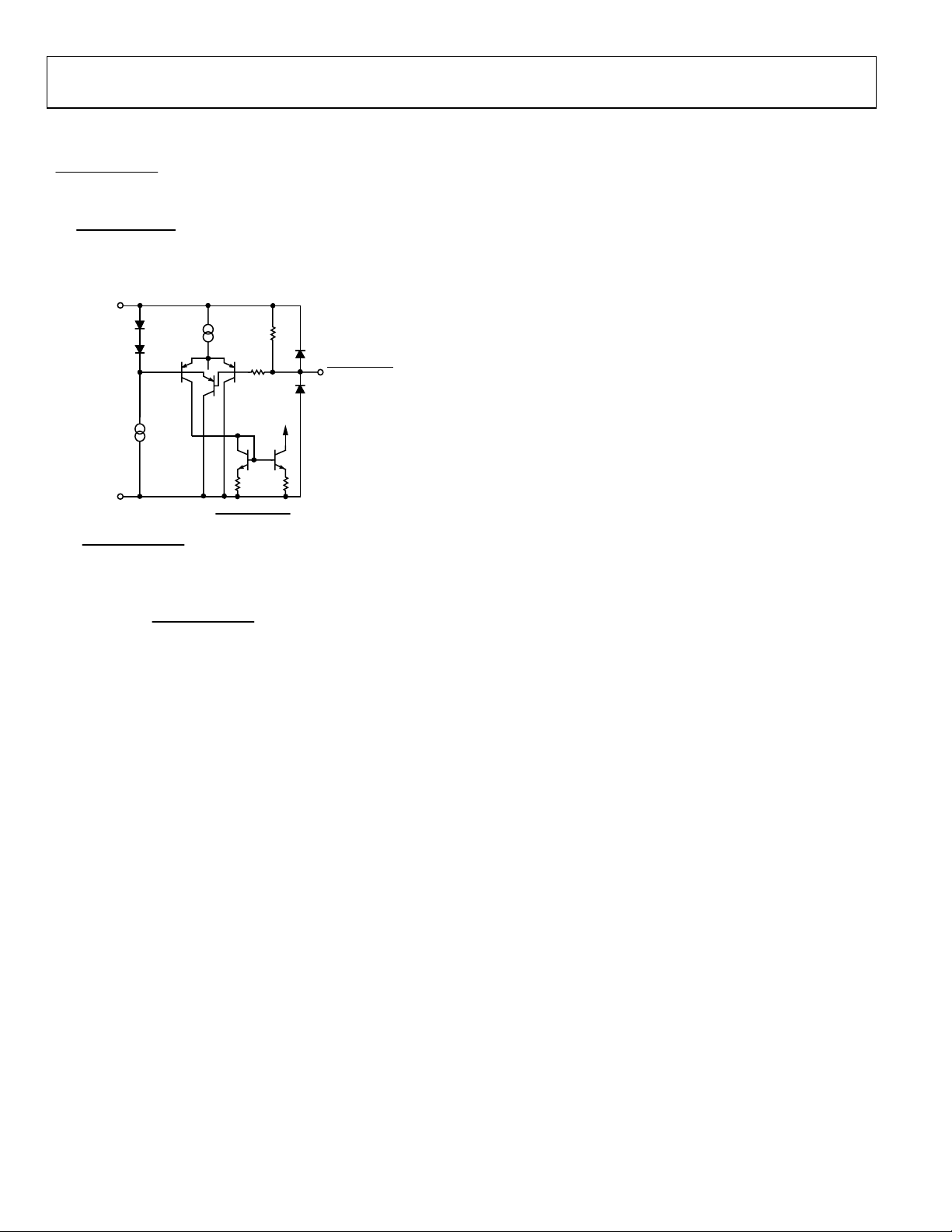
INPUT PROTECTION
The ADA4841-1/ADA4841-2 are fully protected from ESD
events, withstanding ESD events of 2.5 keV with no measured
performance degradation. The precision input is protected
with an ESD network between the power supplies and diode
clamps across the input device pair, as shown in
VCC
BIAS
ESD
VP
ESD
VEE
TO REST OF AMPLIFIER
Figure 46. Input Stage and Protection Diodes
ESD
ESD
Figure 46.
VN
05614-006
For differential voltages above approximately 1.4 V, the diode
clamps start to conduct. Too much current can cause damage
due to excessive heating. If large differential voltages need to be
sustained across the input terminals, it is recommended that the
current through the input clamps be limited to below 150 mA.
Series input resistors sized appropriately for the expected
differential overvoltage provide the needed protection.
The ESD clamps start to conduct for input voltages more than
0.7 V above the positive supply and input voltages more than
0.7 V below the negative supply. It is recommended that the
fault current be limited to less than 150 mA if an overvoltage
condition is expected.
Rev. B | Page 15 of 20
Page 16
ADA4841-1/ADA4841-2
POWER-DOWN OPERATION
Figure 47 shows the ADA4841-1 power-down circuitry. If the
POWER DOWN
input PNP transistor is pulled high through the internal pull-up
resistor to the positive supply, and the part is turned on. Pulling
POWER DOWN
the
supply turns the part off, reducing the supply current to
approximately 40 μA.
VCC
pin is left unconnected, then the base of the
pin approximately 1.7 V below the positive
I
BIAS
ESD
POWER DOWN
ESD
TO
AMPLIFIER
BIAS
VEE
POWER DOWN
The
as shown in
Figure 47.
POWER DOWN
pin is protected with ESD clamps,
Figure 47. Voltages beyond the power supplies
05614-052
Circuit
cause these diodes to conduct. The guidelines for limiting the
overload current in the input protection section should also be
followed for the
POWER DOWN
pin.
Rev. B | Page 16 of 20
Page 17

ADA4841-1/ADA4841-2
C
K
APPLICATIONS
TYPICAL PERFORMANCE VALUES
To reduce design time and eliminate uncertainty Table 6
provides a convenient reference for typical gains, component
values, and performance parameters.
16-BIT ADC DRIVER
The combination of low noise, low power, and high speed
make the ADA4841-1/ADA4841-2 the perfect driver solution
for low power, 16-bit ADCs, such as the
shows a typical 16-bit single-supply application.
There are different challenges to a single-supply, high resolution
design, and the ADA4841-1/ADA4841-2 address these nicely.
In a single-supply system, a main challenge is using the
amplifier in buffer mode with the lowest output noise and
preserving linearity compatible with the ADC.
Rail-to-rail input amplifiers are usually higher noise than the
ADA4841-1/ADA4841-2 and cannot be used in this mode
because of the nonlinear region around the crossover point of
their input stages. The ADA4841-1/ADA4841-2, which has no
crossover region but has a wide linear input range from 100 mV
below ground to 1 V below positive rail, solve this problem, as
shown in
Figure 48. The amplifier, when configured as a
follower, has a linear signal range from 0.25 V above the minus
supply voltage (limited by the amplifier’s output stage) to 1 V
below the positive supply (limited by the amplifier input stage).
A 0 V to +4.096 V signal range can be accommodated with a
positive supply as low as +5.2 V and a negative power supply of
−0.25 V. The 5.2 V supply also allows the use of a small, low
dropout, low temperature drift
ADR364 reference voltage. If
ground is used as the amplifier negative supply, then note that at
the low end of the input range close to ground, the ADA48411/ADA4841-2 exhibits substantial nonlinearity, as any rail-torail output amplifier. The ADA4841-1/ADA4841-2 drive a onepole, low-pass filter. This filter limits the already very low noise
contribution from the amplifier to the
+5.2V
ADR364
33Ω
2.7nF
0V TO 4.096V
ADA4841
100nF
100nF
–0.25V
AD7685. Figure 48
AD7685.
REF
GND
100nF
VDD
AD7685
10μF
IN+
IN–
VIO
SDI
SCK
SDO
CNV
RECONSTRUCTION FILTER
The ADA4841-1/ADA4841-2 can also be used as a reconstruction
filter at the output of DACs for suppression of the sampling
frequency. The filter shown in
Sallen-Key LPF with a fixed gain of G = +1.6.
R1
INPUT
249Ω
Figure 49. Two-Pole 500 kHz Reconstruction Filter Schematic
R2
249Ω
1320pF
Setting the resistors and capacitors equal to each other greatly
simplifies the design equations for the Sallen-Key filter. The
corner frequency, or −3 dB frequency, can be described by
the equation
1
f
=
C
112
R
π
The quality factor, or Q, is shown in the equation
1
Q−=
3
For minimum peaking, set Q equal to 0.707.
The gain, or K, of the amplifier is
R4
R3
1+=
K
Resistor values are kept low for minimal noise contribution,
offset voltage, and optimal frequency response.
Figure 49 is a two-pole, 500 kHz
C2
1320pF
10μF
+5V
0.1μF
C1
840Ω
U1
0.1μF
10μF
–5V
R3
R4
499Ω
OUTPUT
05614-044
05614-060
Figure 48. ADC Driver Schematic
Rev. B | Page 17 of 20
Page 18

ADA4841-1/ADA4841-2
Table 6. Recommended Values and Typical Performance
Peaking
Gain RF (Ω) RG (Ω) −3 dB BW (MHz) Slew Rate (V/μs)
(dB)
+1 0 N/A 77 12.5 0.9 2 2
+2 499 499 34 12.5 0.3 4 5.73
−1 499 499 38 12.5 0.4 4 5.73
+5 499 124 11 12 0 10 11.9
+10 499 54.9 5 12 0 20 21.1
+20 499 26.1 2.3 11.2 0 40 42.2
Output Noise ADA4841-1/
ADA4841-2 Only (nV/√Hz)
Total Output Noise Including
Resistors (nV/√Hz)
Capacitor selection is critical for optimal filter performance.
Capacitors with low temperature coefficients, such as NPO
ceramic capacitors, are good choices for filter elements.
Figure 50
shows the filter response.
5
0
–5
–10
–15
–20
GAIN (dB)
–25
–30
–35
–40
0.03 10
FREQUENCY (MHz)
Figure 50. Filter Frequency Response
10.1
05614-043
LAYOUT CONSIDERATIONS
To ensure optimal performance, careful and deliberate attention
must be paid to the board layout, signal routing, power supply
bypassing, and grounding.
GROUND PLANE
It is important to avoid ground in the areas under and around
the input and output of the ADA4841-1/ADA4841-2. Stray
capacitance created between the ground plane and the input
and output pads of a device are detrimental to high speed
amplifier performance. Stray capacitance at the inverting input,
along with the amplifier input capacitance, lowers the phase
margin and can cause instability. Stray capacitance at the output
creates a pole in the feedback loop. This can reduce phase
margin and can cause the circuit to become unstable.
POWER SUPPLY BYPASSING
Power supply bypassing is a critical aspect in the performance
of the ADA4841-1/ADA4841-2. A parallel connection of
capacitors from each of the power supply pins to ground works
best. A typical connection is shown in
capacitors offer better high frequency response where larger
value electrolytics offer better low frequency performance.
Paralleling different values and sizes of capacitors helps to
ensure that the power supply pins are provided a low ac impedance
across a wide band of frequencies. This is important for minimizing
the coupling of noise into the amplifier. This can be especially
important when the amplifier PSR is starting to roll off—the
bypass capacitors can help lessen the degradation in PSR
performance.
Starting directly at the ADA4841-1/ADA4841-2 power supply
pins, the smallest value capacitor should be placed on the same
side of the board as the amplifier, and as close as possible to the
amplifier power supply pin. The ground end of the capacitor
should be connected directly to the ground plane. Keeping the
capacitors’ distance short but equal from the load is important
and can improve distortion performance. This process should
be repeated for the next largest value capacitor.
It is recommended that a 0.1 μF ceramic 0508 case be used. The
0508 case size offers low series inductance and excellent high
frequency performance. A 10 μF electrolytic capacitor should be
placed in parallel with the 0.1 μF capacitor. Depending on the
circuit parameters, some enhancement to performance can be
realized by adding additional capacitors. Each circuit is different
and should be individually analyzed for optimal performance.
Figure 49. Smaller value
Rev. B | Page 18 of 20
Page 19

ADA4841-1/ADA4841-2
OUTLINE DIMENSIONS
5.00 (0.1968)
4.80 (0.1890)
4.00 (0.1574)
3.80 (0.1497)
85
6.20 (0.2440)
5.80 (0.2284)
41
1.27 (0.0500)
BSC
0.25 (0.0098)
0.10 (0.0040)
COPLANARITY
0.10
CONTROLLING DIMENSIONS ARE IN MILLIMETERS; INCH DIMENSIONS
(IN PARENTHESES) ARE ROUNDED-OFF MILLIMETER EQUIVALENTS FOR
REFERENCE ONLY AND ARE NOT APPROPRIATE FOR USE IN DESIGN.
SEATING
PLANE
COMPLIANT TO JEDEC STANDARDS MS-012-AA
1.75 (0.0688)
1.35 (0.0532)
0.51 (0.0201)
0.31 (0.0122)
0.25 (0.0098)
0.17 (0.0067)
0.50 (0.0196)
0.25 (0.0099)
8°
1.27 (0.0500)
0°
0.40 (0.0157)
× 45°
Figure 51. 8-Lead Standard Small Outline Package [SOIC_N]
Narrow Body (R-8)
Dimensions shown in millimeters and (inches)
3.20
3.00
2.80
8
5
4
SEATING
PLANE
5.15
4.90
4.65
1.10 MAX
0.23
0.08
8°
0°
0.80
0.60
0.40
3.20
3.00
2.80
PIN 1
0.95
0.85
0.75
0.15
0.00
COPLANARITY
1
0.65 BSC
0.38
0.22
0.10
COMPLIANT TO JEDEC STANDARDS MO-187-AA
Figure 52. 8-Lead Mini Small Outline Package [MSOP]
(RM-8)
Dimensions shown in millimeters
Rev. B | Page 19 of 20
Page 20

ADA4841-1/ADA4841-2
ORDERING GUIDE
Model Temperature Range Package Description Package Option Ordering Quantity
ADA4841-1YRZ
ADA4841-1YRZ-R7
ADA4841-1YRZ-RL
ADA4841-2YRMZ
ADA4841-2YRMZ-R7
ADA4841-2YRMZ-RL
1
Z = Pb-free part.
1
1
1
1
1
1
−40°C to +125°C 8-Lead SOIC_N R-8 1
−40°C to +125°C 8-Lead SOIC_N R-8 1,000
−40°C to +125°C 8-Lead SOIC_N R-8 2,500
−40°C to +125°C 8-Lead MSOP RM-8 1
−40°C to +125°C 8-Lead MSOP RM-8 1,000
−40°C to +125°C 8-Lead MSOP RM-8 3,000
© 2005 Analog Devices, Inc. All rights reserved. Trademarks and
registered trademarks are the property of their respective owners.
D05614–0–10/05(B)
Rev. B | Page 20 of 20
Page 21

 Loading...