

Page 1

30 V Zero-Drift, Rail-to-Rail Output
–
A
Data Sheet
FEATURES
Single supply operation: 4.5 V to 30 V
Dual supply operation: ±2.25 V to ±15 V
Low offset voltage: 4 μV maximum
Input offset voltage drift: 0.05 μV/°C maximum
High gain: 130 dB minimum
High PSRR: 120 dB minimum
High CMRR: 130 dB minimum
Input common-mode range includes lower supply rail
Rail-to-rail output
Low supply current: 0.95 mA maximum
APPLICATIONS
Electronic weigh scale
Pressure and position sensors
Strain gage amplifiers
Medical instrumentation
Thermocouple amplifiers
Precision Amplifier
ADA4638-1
PIN CONFIGURATIONS
DA4638-1
1
NC
IN
2
TOP VIEW
(Not to Scale)
+IN
3
V–
4
NOTES
1. NC = NO CONNECT. DO NOT
CONNECT TO THI S PIN.
Figure 1. 8-Lead SOIC
ADA4638-1
1NC
2–IN
TOP VIEW
(Not to Scale)
3+IN
4V–
NOTES
1. NC = NO CONNECT. DO NOT CONNECT TO THI S PIN.
2. IT I S RECOMMENDE D THAT THE EXPOSED PAD BE
CONNECTED TO V–.
Figure 2. 8-Lead LFCSP
8
NC
V+
7
OUT
6
NC
5
8NC
7V+
6OUT
5NC
10072-001
10072-002
GENERAL DESCRIPTION
The ADA4638-1 is a high voltage, high precision, zero-drift
amplifier featuring rail-to-rail output swing. It is guaranteed to
operate from 4.5 V to 30 V single supply or ±2.25 V to ±15 V
dual supplies while consuming less than 0.95 mA of supply
current at ±5 V.
With an offset voltage of 4 µV, offset drift less than 0.05 µV/°C,
no 1/f noise, and input voltage noise of only 1.2 µV p-p (0.1 Hz
to 10 Hz), the ADA4638-1 is suited for high precision applications
where large error sources cannot be tolerated. Pressure sensors,
medical equipment, and strain gage amplifiers benefit greatly
from nearly zero drift over the wide operating temperature
range. Many applications can take advantage of the rail-to-rail
output swing provided by the ADA4638-1 to maximize the signalto-noise ratio (SNR).
The ADA4638-1 is specified for the extended industrial (−40°C
to +125°C) temperature range and is available in 8-lead LFCSP
(3 mm × 3 mm) and SOIC packages.
Table 1. Analog Devices, Inc., Zero-Drift Op Amp Portfolio
Operating
Voltage Type Product
Offset
Voltage
(μV) Max
Offset
Voltage Drift
(μV/°C) Max
30 V Single ADA4638-1 4.5 0.08
Single AD8638 9 0.06 16 V
Dual AD8639 9 0.06
5 V
Single
ADA4528-1 2.5 0.015
AD8628 5 0.02
AD8538 13 0.1
ADA4051-1 15 0.1
Dual
AD8629 5 0.02
AD8539 13 0.1
ADA4051-2 15 0.1
Quad AD8630 5 0.02
Rev. 0
Information furnished by Analog Devices is believed to be accurate and reliable. However, no
responsibility is assumed by Anal og Devices for its use, nor for any infringements of patents or ot her
rights of third parties that may result from its use. Specifications subject to change without notice. No
license is granted by implication or otherwise under any patent or patent rights of Analog Devices.
Trademarks and registered trademarks are the property of their respective owners.
One Technology Way, P.O. Box 9106, Norwood, MA 02062-9106, U.S.A.
Tel: 781.329.4700 www.analog.com
Fax: 781.461.3113 ©2011 Analog Devices, Inc. All rights reserved.
Page 2

ADA4638-1 Data Sheet
TABLE OF CONTENTS
Features.............................................................................................. 1
Applications....................................................................................... 1
Pin Configurations ........................................................................... 1
General Description ......................................................................... 1
Revision History ............................................................................... 2
Specifications..................................................................................... 3
Electrical Characteristics—30 V Operation ............................. 3
Electrical Characteristics—10 V Operation ............................. 4
Electrical Characteristics—5 V Operation................................ 5
Absolute Maximum Ratings............................................................ 6
Thermal Resistance ...................................................................... 6
ESD Caution.................................................................................. 6
REVISION HISTORY
10/11—Revision 0: Initial Version
Typical Performance Characteristics..............................................7
Applications Information.............................................................. 16
Differentiation ............................................................................ 16
Theory of Operation .................................................................. 17
Input Protection ......................................................................... 17
No Output Phase Reversal ........................................................ 17
Noise Considerations................................................................. 18
Comparator Operation.............................................................. 18
Precision Low-Side Current Shunt Sensor.............................. 20
Printed Circuit Board Layout................................................... 20
Outline Dimensions....................................................................... 21
Ordering Guide .......................................................................... 21
Rev. 0 | Page 2 of 24
Page 3

Data Sheet ADA4638-1
SPECIFICATIONS
ELECTRICAL CHARACTERISTICS—30 V OPERATION
VS = 30 V, VCM = VSY/2 V, TA = 25°C, unless otherwise specified.
Table 2.
Parameter Symbol Test Conditions/Comments Min Typ Max Unit
INPUT CHARACTERISTICS
Offset Voltage VOS 0.5 4.5 V
−40°C ≤ TA ≤ +125°C; SOIC 12.5 V
−40°C ≤ TA ≤ +125°C; LFCSP 14.5 V
Offset Voltage Drift ∆VOS/∆T −40°C ≤ TA ≤ +125°C; SOIC 0.08 V/°C
−40°C ≤ TA ≤ +125°C; LFCSP 0.1 V/°C
Input Bias Current IB 45 90 pA
−40°C ≤ TA ≤ +125°C 500 pA
Input Offset Current IOS 25 105 pA
−40°C ≤ TA ≤ +125°C 170 pA
Input Voltage Range 0 27 V
Common-Mode Rejection Ratio CMRR VCM = 0 V to 27 V 130 142 dB
−40°C ≤ TA ≤ +125°C 130 dB
Open-Loop Gain AVO R
−40°C ≤ TA ≤ +125°C 140 dB
Input Resistance, Common Mode R
Input Capacitance, Differential Mode C
Input Capacitance, Common Mode C
INCM
INDM
INCM
OUTPUT CHARACTERISTICS
Output Voltage High VOH R
−40°C ≤ TA ≤ +125°C 29.85 V
R
−40°C ≤ TA ≤ +125°C 29.35 V
Output Voltage Low VOL R
−40°C ≤ TA ≤ +125°C 95 mV
R
−40°C ≤ TA ≤ +125°C 445 mV
Short-Circuit Current ISC ±38 mA
Closed-Loop Output Impedance Z
f = 1 MHz, AV = +1 220 Ω
OUT
POWER SUPPLY
Power Supply Rejection Ratio PSRR VS = 4.5 V to 30 V 120 143 dB
−40°C ≤ TA ≤ +125°C 120 dB
Supply Current/Amplifier ISY I
−40°C ≤ TA ≤ +125°C 1.25 mA
DYNAMIC PERFORMANCE
Slew Rate SR RL = 10 kΩ, CL = 20 pF, AV = +1 1.5 V/s
Overload Recovery Time RL = 10 kΩ, CL = 20 pF, AV = −100 8 s
Settling Time to 0.1% tS V
Unity-Gain Crossover UGC VIN = 30 mV p-p, RL = 10 kΩ, CL = 20 pF, AV = +1
Phase Margin ΦM V
Gain-Bandwidth Product GBP VIN = 30 mV p-p, RL = 10 kΩ, CL = 20 pF, AV = +100 1.5 MHz
−3 dB Closed-Loop Bandwidth f
V
−3dB
NOISE PERFORMANCE
Voltage Noise en p-p f = 0.1 Hz to 10 Hz 1.2 µV p-p
Voltage Noise Density en f = 1 kHz 66 nV/√Hz
Current Noise Density in f = 1 kHz 0.1 pA/√Hz
= 10 kΩ, VO = 1 V to 29 V 140 165 dB
L
= 10 kΩ to VCM 29.90 29.92 V
L
= 2 kΩ to VCM 29.50 29.58 V
L
= 10 kΩ to VCM 50 60 mV
L
= 2 kΩ to VCM 235 270 mV
L
= 0 mA 0.85 1.05 mA
O
= 5 V step, RL = 10 kΩ, CL = 20 pF, AV = −1 4 µs
IN
= 30 mV p-p, RL = 10 kΩ, CL = 20 pF, AV = +1 69 Degrees
IN
= 30 mV p-p, RL = 10 kΩ, CL = 20 pF, AV = +1 2.5 MHz
IN
Rev. 0 | Page 3 of 24
330 GΩ
4 pF
9 pF
1.3
MHz
Page 4

ADA4638-1 Data Sheet
ELECTRICAL CHARACTERISTICS—10 V OPERATION
VS = 10 V, VCM = VSY/2 V, TA = 25°C, unless otherwise specified.
Table 3.
Parameter Symbol Test Conditions/Comments Min Typ Max Unit
INPUT CHARACTERISTICS
Offset Voltage VOS 0.1 4 V
−40°C ≤ TA ≤ +125°C; SOIC 9 V
−40°C ≤ TA ≤ +125°C; LFCSP 12 V
Offset Voltage Drift ∆VOS/∆T −40°C ≤ TA ≤ +125°C; SOIC 0.05 V/°C
−40°C ≤ TA ≤ +125°C; LFCSP 0.08 V/°C
Input Bias Current IB 20 50 pA
−40°C ≤ TA ≤ +125°C 250 pA
Input Offset Current IOS 20 80 pA
−40°C ≤ TA ≤ +125°C 140 pA
Input Voltage Range 0 7 V
Common-Mode Rejection Ratio CMRR VCM = 0 V to 7 V 130 155 dB
−40°C ≤ TA ≤ +125°C 130 dB
Open-Loop Gain AVO R
−40°C ≤ TA ≤ +125°C 130 dB
Input Resistance, Common Mode R
Input Capacitance, Differential Mode C
Input Capacitance, Common Mode C
INCM
INDM
INCM
OUTPUT CHARACTERISTICS
Output Voltage High VOH R
−40°C ≤ TA ≤ +125°C 9.95 V
R
−40°C ≤ TA ≤ +125°C 9.75 V
Output Voltage Low VOL R
−40°C ≤ TA ≤ +125°C 40 mV
R
−40°C ≤ TA ≤ +125°C 145 mV
Short-Circuit Current ISC ±22 mA
Closed-Loop Output Impedance Z
f = 1 MHz, AV = +1 300 Ω
OUT
POWER SUPPLY
Power Supply Rejection Ratio PSRR VS = 4.5 V to 30 V 120 143 dB
−40°C ≤ TA ≤ +125°C 120 dB
Supply Current/Amplifier ISY I
−40°C ≤ TA ≤ +125°C 1.15 mA
DYNAMIC PERFORMANCE
Slew Rate SR RL = 10 kΩ, CL = 20 pF, AV = +1 1.5 V/s
Overload Recovery Time RL = 10 kΩ, CL = 20 pF, AV = −100 14 s
Settling Time to 0.1% tS V
Unity-Gain Crossover
UGC VIN = 30 mV p-p, RL = 10 kΩ, CL = 20 pF, AV = +1
Phase Margin ΦM V
Gain Bandwidth Product GBP VIN = 30 mV p-p, RL = 10 kΩ, CL = 20 pF, AV = +100 1.4 MHz
−3 dB Closed-Loop Bandwidth f
V
−3dB
NOISE PERFORMANCE
Voltage Noise en p-p f = 0.1 Hz to 10 Hz 1.2 µV p-p
Voltage Noise Density en f = 1 kHz 66 nV/√Hz
Current Noise Density in f = 1 kHz 0.1 pA/√Hz
= 10 kΩ, VO = 1 V to 9 V 130 160 dB
L
= 10 kΩ to VCM 9.96 9.97 V
L
= 2 kΩ to VCM 9.85 9.86 V
L
= 10 kΩ to VCM 20 25 mV
L
= 2 kΩ to VCM 80 90 mV
L
= 0 mA 0.8 0.95 mA
O
= 2 V step, RL = 10 kΩ, CL = 20 pF, AV = −1 3 µs
IN
= 30 mV p-p, RL = 10 kΩ, CL = 20 pF, AV = +1 67 Degrees
IN
= 30 mV p-p, RL = 10 kΩ, CL = 20 pF, AV = +1 1.9 MHz
IN
250 GΩ
4 pF
9 pF
1.1
MHz
Rev. 0 | Page 4 of 24
Page 5

Data Sheet ADA4638-1
ELECTRICAL CHARACTERISTICS—5 V OPERATION
VS = 5 V, VCM = VSY/2 V, TA = 25°C, unless otherwise specified.
Table 4.
Parameter Symbol Test Conditions/Comments Min Typ Max Unit
INPUT CHARACTERISTICS
Offset Voltage VOS 1 13 V
−40°C ≤ TA ≤ +125°C; SOIC 18 V
−40°C ≤ TA ≤ +125°C; LFCSP 21 V
Offset Voltage Drift ∆VOS/∆T −40°C ≤ TA ≤ +125°C; SOIC 0.05 V/°C
−40°C ≤ TA ≤ +125°C; LFCSP 0.08 V/°C
Input Bias Current IB 30 90 pA
−40°C ≤ TA ≤ +125°C 230 pA
Input Offset Current IOS 60 170 pA
−40°C ≤ TA ≤ +125°C 200 pA
Input Voltage Range 0 3 V
Common-Mode Rejection Ratio CMRR VCM = 0 V to 3 V 118 140 dB
−40°C ≤ TA ≤ +125°C 118 dB
Open-Loop Gain AVO R
−40°C ≤ TA ≤ +125°C 125 dB
Input Resistance, Common Mode R
Input Capacitance, Differential Mode C
Input Capacitance, Common Mode C
INCM
INDM
INCM
OUTPUT CHARACTERISTICS
Output Voltage High VOH R
−40°C ≤ TA ≤ +125°C 4.97 V
R
−40°C ≤ TA ≤ +125°C 4.87 V
Output Voltage Low VOL R
−40°C ≤ TA ≤ +125°C 15 mV
R
−40°C ≤ TA ≤ +125°C 70 mV
Short-Circuit Current ISC ±22 mA
Closed-Loop Output Impedance Z
f = 1 MHz, AV = +1 340 Ω
OUT
POWER SUPPLY
Power Supply Rejection Ratio PSRR VS = 4.5 V to 30 V 120 143 dB
−40°C ≤ TA ≤ +125°C 120 dB
Supply Current/Amplifier ISY I
−40°C ≤ TA ≤ +125°C 1.15 mA
DYNAMIC PERFORMANCE
Slew Rate SR RL = 10 kΩ, CL = 20 pF, AV = +1 1.5 V/s
Overload Recovery Time RL = 10 kΩ, CL = 20 pF, AV = −100 22 s
Settling Time to 0.1% tS V
Unity-Gain Crossover UGC VIN = 20 mV p-p, RL = 10 kΩ, CL = 20 pF, AV = +1 1.0 MHz
Phase Margin ΦM V
Gain Bandwidth Product GBP VIN = 20 mV p-p, RL = 10 kΩ, CL = 20 pF, AV = +100 1.3 MHz
−3 dB Closed-Loop Bandwidth f
V
−3dB
NOISE PERFORMANCE
Voltage Noise en p-p f = 0.1 Hz to 10 Hz 1.2 µV p-p
Voltage Noise Density en f = 1 kHz 70 nV/√Hz
Current Noise Density in f = 1 kHz 0.015 pA/√Hz
= 10 kΩ, VO = 0.5 V to +4.5 V 125 150 dB
L
= 10 kΩ to VCM 4.98 4.984 V
L
= 2 kΩ to VCM 4.90 4.92 V
L
= 10 kΩ to VCM 7.5 10 mV
L
= 2 kΩ to VCM 37 45 mV
L
= 0 mA 0.8 0.95 mA
O
= 1 V step, RL = 10 kΩ, CL = 20 pF, AV = −1 3 µs
IN
= 20 mV p-p, RL = 10 kΩ, CL = 20 pF, AV = +1 64 Degrees
IN
= 20 mV p-p, RL = 10 kΩ, CL = 20 pF, AV = +1 1.8 MHz
IN
75 GΩ
4 pF
9 pF
Rev. 0 | Page 5 of 24
Page 6

ADA4638-1 Data Sheet
ABSOLUTE MAXIMUM RATINGS
Table 5.
Parameter Rating
Supply Voltage 33 V
Input Voltage1 ±VSY
Input Current ±10 mA
Differential Input Voltage ±V
Output Short-Circuit Duration to GND Indefinite
Storage Temperature Range −65°C to +150°C
Operating Temperature Range −40°C to +125°C
Junction Temperature Range −65°C to +150°C
Lead Temperature (Soldering, 60 sec) 300°C
1
Input voltage should always be limited to less than 30 V.
SY
Stresses above those listed under Absolute Maximum Ratings
may cause permanent damage to the device. This is a stress
rating only; functional operation of the device at these or any
other conditions above those indicated in the operational
section of this specification is not implied. Exposure to absolute
maximum rating conditions for extended periods may affect
device reliability.
THERMAL RESISTANCE
θJA is specified for a device soldered on a 4-layer JEDEC
standard board with zero airflow. For LFCSP packages, the
exposed pad is soldered to the board.
Table 6. Thermal Resistance
Package Type θJA θ
8-Lead SOIC 120 45 °C/W
8-Lead LFCSP 75 12 °C/W
Unit
JC
ESD CAUTION
Rev. 0 | Page 6 of 24
Page 7

Data Sheet ADA4638-1
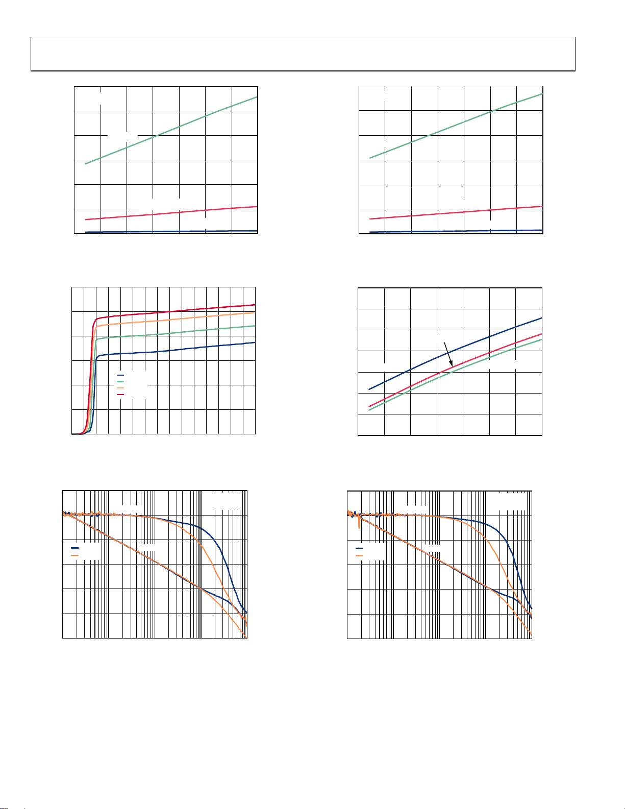
TYPICAL PERFORMANCE CHARACTERISTICS
TA = 25°C, unless otherwise noted.
12
10
VSY= ±2.5V
V
CM=VSY
150 UNITS
/2
30
25
VSY= ±15V
V
CM=VSY
150 UNITS
/2
8
6
4
NUMBER OF AMPLIF IERS
2
0
–9–8–7–6–5–4–3–2–1
–10
OFFSET VOLTAGE (µV)
012345678
Figure 3. Input Offset Voltage Distribution
20
18
16
14
12
10
8
6
NUMBER OF AMPLIFI ERS
4
2
0
0 0.010.020.030.040.050.060.070.08
TCVOS(µV/°C)
VSY= ±2.5V
V
–40°C < T
140 LFCSP UNITS
CM=VSY
/2
< +125°C
A
Figure 4. Input Offset Voltage Drift Distribution
20
15
10
NUMBER OF AMPLIFIERS
5
9
10
10072-003
0
–5.0
–4.5
–4.0
–3.5
–3.0
–2.5
–2.0
OFFSET VOLTAGE (µV)
0
0.5
1.0
1.5
2.0
2.5
3.0
3.5
4.0
4.5
–1.5
–1.0
–0.5
5.0
10072-006
Figure 6. Input Offset Voltage Distribution
14
VSY= ±15V
/2
12
10
8
6
4
NUMBER OF AMPLIFIERS
2
0
0 0.01 0.02 0.03 0.04 0.05 0.06 0.07 0.08
10072-004
TCVOS(µV/°C)
V
CM=VSY
–40°C < T
140 LFCSP UNITS
< +125°C
A
10072-007
Figure 7. Input Offset Voltage Drift Distribution
30
25
20
15
10
NUMBER OF AMPLI FIERS
5
0
0 0.010.020.030.040.050.060.070.08
TCVOS (µV/°C)
VSY= ±2.5V
V
/2
CM=VSY
–40°C ≤ T
140 SOIC UNITS
≤ +125°C
A
Figure 5. Input Offset Voltage Drift Distribution
10072-105
Rev. 0 | Page 7 of 24
18
16
14
12
10
8
6
NUMBER OF AMPLI FIERS
4
2
0
0 0.010.020.030.040.050.060.070.08
TCVOS (µV/°C)
VSY=±15V
/2
V
CM=VSY
–40°C ≤ T
140 SOIC UNITS
≤ +125°C
A
Figure 8. Input Offset Voltage Drift Distribution
10072-108
Page 8

ADA4638-1 Data Sheet
T
10
VSY= ±2.5V
8
6
4
2
AGE (µV)
0
–2
–4
OFFSET VOL
–6
–8
–10
0 0.5 1.0 1.5 2.0 2.5 3.0 3.5 4.0
COMMON-MODE VOLTAGE (V)
Figure 9. Input Offset Voltage vs. Common-Mode Voltage
10072-005
10
VSY=±15V
8
6
4
2
0
–2
–4
OFFSET VOLTAGE (µV)
–6
–8
–10
0 2 4 6 8 10 12 14 16 18 20 22 24 26 28 30
COMMON-MODE VOLTAGE (V)
Figure 12. Input Offset Voltage vs. Common-Mode Voltage
10072-008
200
150
100
50
0
–50
INPUT BIAS CURRENT (pA)
–100
–150
–50 –25 0 25 50 75 100 125
TEMPERATURE (°C)
I
IB+
–
B
V
SY
= ±2.5V
Figure 10. Input Bias Current vs. Temperature
150
VSY= ±2.5V
100
50
–
I
B
0
–50
INPUT BIAS CURRENT (pA)
–100
IB+
150
100
50
0
–50
–100
–150
INPUT BIAS CURRENT (pA)
–200
–250
–50 –25 0 25 50 75 100 125
10072-009
TEMPERATURE (°C)
IB+
–
I
B
V
SY
= ±15V
10072-012
Figure 13. Input Bias Current vs. Temperature
150
VSY=±15V
100
50
0
IB+
–50
INPUT BIAS CURRENT (pA)
–100
–
I
B
–150
0 0.5 1.0 1.5 2.0 2. 5 3.0
COMMON-MODE VOLTAGE (V)
Figure 11. Input Bias Current vs. Common-Mode Voltage
10072-010
–150
0 3 6 9 121518212427
COMMON-MODE VOLTAGE (V)
Figure 14. Input Bias Current vs. Common-Mode Voltage
10072-013
Rev. 0 | Page 8 of 24
Page 9

Data Sheet ADA4638-1
T
10
VSY= ±2.5V
1
100
VSY= ±15V
10
0.1
) TO SUPPLY RAIL (V)
0.01
OL
AGE (V
1m
0.1m
OUTPUT VOL
0.01m
Figure 15. Output Voltage (V
10
0.1
) TO SUPPLY RAIL (V)
0.01
OH
1m
0.1m
OUTPUT VOLTAGE (V
0.01m
Figure 16. Output Voltage (V
–40°C
+25°C
+85°C
+125°C
0.001 0. 01 0.1 1 10 100
VSY= ±2.5V
1
–40°C
+25°C
+85°C
+125°C
0.001 0. 01 0.1 1 10 100
LOAD CURRENT (mA)
) to Supply Rail vs. Load Current
OL
LOAD CURRENT (mA)
) to Supply Rail vs. Load Current
OH
70
VSY= ±2.5V
60
50
40
) TO SUPPLY RAIL (mV)
OL
OU TP U T V OLTA G E ( V
RL = 2kΩ
30
20
10
0
–50 –25 0 25 50 75 100 125
Figure 17. Output Voltage (V
RL = 10kΩ
RL = 100kΩ
TEMPERATURE (°C)
) to Supply Rail vs. Temperature
OL
–40°C
+25°C
1
) TO SUPPLY RAIL (V)
OL
0.1
0.01
10072-011
OU T PU T VO LTAG E (V
0.001
Figure 18. Output Voltage (V
+85°C
+125°C
0.001 0. 01 0.1 1 10 100
LOAD CURRENT (mA)
) to Supply Rail vs. Load Current
OL
10072-014
100
VSY= ±15V
10
–40°C
+25°C
1
) TO SUPPLY RAIL (V)
OH
0.1
0.01
10072-015
OU TPU T VO LTAG E (V
1m
0.001 0.01 0.1 1 10 100
Figure 19. Output Voltage (V
+85°C
+125°C
LOAD CURRENT (mA)
) to Supply Rail vs. Load Current
OH
10072-018
450
VSY= ±15V
400
350
300
250
) TO SUPPLY RAIL (mV)
OL
200
150
100
50
OUTPUT VOLTAGE (V
10072-016
Figure 20. Output Voltage (V
RL = 2kΩ
0
–50 –25 0
RL = 10kΩ
RL = 100kΩ
25 50 75
TEMPERATURE (°C)
) to Supply Rail vs. Temperature
OL
100 125
10072-019
Rev. 0 | Page 9 of 24
Page 10
ADA4638-1 Data Sheet
R
R
120
VSY= ±2.5V
100
80
) TO SUPPLY RAIL (mV)
60
OH
40
20
OUTPUT VOLTAGE (V
0
–50 –25 0 25 50 75 100 125
Figure 21. Output Voltage (V
1.2
1.0
0.8
AMPLIFIER (mA)
0.6
0.4
0.2
SUPPLY CURRENT PE
0
024681012141618202224262830
RL = 2kΩ
TEMPERATURE (° C)
–40°C
+25°C
+85°C
+125°C
SUPPLY VOLTAGE (V)
RL = 10kΩ
) to Supply Rail vs. Temperature
OH
Figure 22. Supply Current vs. Supply Voltage
80
60
PHASE
RL = 100kΩ
VSY=±2.5V
R
= 10kΩ
L
135
90
600
VSY= ±15V
500
400
RL = 2kΩ
) TO SUPPLY RAIL (mV)
300
OH
200
100
OUTPUT VOLTAGE (V
0
–50 –25 0 25 50 75 100 125
10072-017
Figure 24. Output Voltage (V
RL = 10kΩ
RL = 100kΩ
TEMPERATURE (°C)
) to Supply Rail vs. Temperature
OH
10072-020
1.2
1.1
1.0
AMPLIFIER (mA)
0.9
VSY=±15V
0.8
0.7
0.6
SUPPLY CURRENT PE
0.5
–50 –25 0 25 50 75 100 125
10072-021
VSY=±5V
TEMPERATURE (°C)
V
SY
=±2.5V
10072-024
Figure 25. Supply Current vs. Temperature
80
60
PHASE
VSY=±15V
= 10kΩ
R
L
135
90
40
20pF
200pF
20
GAIN (dB)
0
–20
–40
1k 10k 100k 1M 10M
GAIN
FREQUENCY (Hz)
Figure 23. Open-Loop Gain and Phase vs. Frequency
45
0
PHASE (Degrees)
–45
–90
–135
10072-022
Rev. 0 | Page 10 of 24
40
20pF
200pF
20
GAIN (dB)
0
–20
–40
1k 10k 100k 1M 10M
GAIN
FREQUENCY (Hz)
Figure 26. Open-Loop Gain and Phase vs. Frequency
45
0
–45
–90
–135
PHASE (Degrees)
10072-025
Page 11

Data Sheet ADA4638-1
60
50
AV = +100
40
30
AV = +10
20
10
–10
CLOSED-LOOP GAIN (dB)
–20
–30
–40
AV = +1
0
10 100 1k 10k 100k 1M 10M
FREQUENCY (Hz )
VSY=±2.5V
= 10kΩ
R
L
Figure 27. Closed-Loop Gain vs. Frequency
10072-023
60
50
AV = +100
40
30
AV = +10
20
10
–10
CLOSED-LOOP GAIN (dB)
–20
–30
–40
AV = +1
0
10 100 1k 10k 100k 1M 10M
FREQUENCY (Hz )
VSY= ±15V
= 10kΩ
R
L
Figure 30. Closed-Loop Gain vs. Frequency
10072-026
120
100
80
60
CMRR (dB)
40
20
0
100 1k 10k 100k 1M 10M
FREQUENC Y (Hz)
VSY=±2.5V
V
CM=VSY
Figure 28. CMRR vs. Frequency
140
120
100
80
60
PSRR (dB)
40
20
PSRR+
PSRR–
VSY=±2.5V
V
CM=VSY
120
/2
10072-027
100
80
60
CMRR (dB)
40
20
0
100 1k 10k 100k 1M 10M
FREQUENC Y (Hz)
VSY=±15V
V
CM=VSY
/2
10072-030
Figure 31. CMRR vs. Frequency
140
/2
120
100
80
60
PSRR (dB)
40
20
PSRR+
PSRR–
V
=±15V
SY
V
CM=VSY
/2
0
–20
100 1k 10k 100k 1M 10M
FREQUENCY (Hz)
Figure 29. PSRR vs. Frequency
10072-028
Rev. 0 | Page 11 of 24
0
–20
100 1k 10k 100k 1M 10M
FREQUENCY (Hz)
Figure 32. PSRR vs. Frequency
10072-031
Page 12
ADA4638-1 Data Sheet
100
1k
VSY=±2.5V
V
CM=VSY
/2
AV = +10
100
1k
VSY= ±15V
V
CM=VSY
/2
AV = +10
10
(Ω)
1
OUT
Z
0.1
0.01
1m
100 1k 10k 100k 1M 10M
AV = +100
AV = +1
FREQUE NCY (Hz)
Figure 33. Closed-Loop Output Impedance vs. Frequency
VSY= ±2.5V
=1V p-p
V
IN
= +1
A
VOLTAGE (0.5V/DIV)
V
R
L
C
L
=10kΩ
=100pF
10
(Ω)
1
OUT
Z
0.1
0.01
1m
100 1k 10k 100k 1M 10M
10072-029
AV = +100
AV = +1
FREQUE NCY (Hz)
10072-032
Figure 36. Closed-Loop Output Impedance vs. Frequency
VSY=±15V
=24V p-p
V
VOLTAGE (5V/DIV)
IN
A
V
R
L
C
L
= +1
=10kΩ
=100pF
TIME (1µs/DIV)
Figure 34. Large Signal Transient Response
VSY= ±2.5V
V
=100mV p-p
IN
A
= +1
VOLTAGE (20mV/DIV)
V
R
=10kΩ
L
C
=100pF
L
TIME (1µs/DIV)
Figure 35. Small Signal Transient Response
10072-033
TIME (10µs/DIV)
10072-036
Figure 37. Large Signal Transient Response
VSY=±15V
V
=100mV p-p
IN
A
= +1
VOLTAGE (20mV/DIV)
10072-034
V
R
=10kΩ
L
C
=100pF
L
TIME (1µs/DIV)
10072-037
Figure 38. Small Signal Transient Response
Rev. 0 | Page 12 of 24
Page 13

Data Sheet ADA4638-1
T
80
VSY= ±2.5V
70
V
= 100mV p -p
IN
A
= +1
V
60
R
=10kΩ
L
50
40
30
OVERSHOOT (%)
20
10
OS+
OS–
0
1 10 100 1000
LOAD CAPACITANCE (pF)
Figure 39. Small Signal Overshoot vs. Load Capacitance
0.1
0
–0.1
INPUT VOLTAGE (V)
–0.2
VSY=±2.5V
= –100
A
V
=100mV p-p
V
IN
=10kΩ
R
L
=100pF
C
L
10072-035
3
2
1
80
VSY= ±15V
70
60
50
40
30
OVERSHOOT (%)
20
10
0
=100mV p-p
V
IN
= +1
A
V
=10kΩ
R
L
OS+
OS–
1 10 100 1000
LOAD CAPACITANCE (pF)
Figure 42. Small Signal Overshoot vs. Load Capacitance
0.5
0
–0.5
IN PUT VO LTA GE ( V)
–1.0
VSY=±15V
= –100
A
V
=500mV p-p
V
IN
=10kΩ
R
L
=100pF
C
L
10072-038
20
15
10
5
0
OUTPUT VOLTAGE (V)
TIME (10µs/DI V)
Figure 40. Positive Overload Recovery
0.2
0.1
0
INPUT VOLTAGE (V)
–0.1
VSY= ±2.5V
= –100
A
V
=100mV p-p
V
IN
=10kΩ
R
L
=100pF
C
L
TIME (10µs/DI V)
–1
10072-039
TIME (10µs/DIV )
Figure 43. Positive Overload Recovery
1.0
0.5
AGE (V)
0
INPUT VOL
–0.5
1
0
–1
–2
OUTPUT VOLTAGE (V)
–3
10072-040
Figure 44. Negative Overload Recovery
TIME (10µs/DIV)
VSY= ±15V
A
= –100
V
V
=500mV p-p
IN
R
=10kΩ
L
C
=100pF
L
0
–5
5
0
–5
–10
–15
–20
OUTPUT VOLTAGE (V)
10072-042
OUTPUT VOLTAGE (V)
10072-043
Figure 41. Negative Overload Recovery
Rev. 0 | Page 13 of 24
Page 14

ADA4638-1 Data Sheet
INPUT
OUTPUT
VSY = ±2.5V
A
= –1
V
R
= 10kΩ
L
+5mV
–5mV
10072-041
VOLTAGE (1V/DIV)
ERROR BAND
POST GAIN = 5
TIME (2µs/DIV)
Figure 45. Positive Settling Time to 0.1%
INPUT
OUTPUT
VSY = ±2.5V
= –1
A
V
= 10kΩ
R
L
+5mV
–5mV
10072-045
VOLTAGE (1V/DIV)
ERROR BAND
POST GAIN = 5
TIME (2µs/DIV)
Figure 46. Negative Settling Time to 0.1%
VOLTAGE (5V/DIV)
ERROR BAND
POST GAIN = 5
TIME (2µs/DIV)
Figure 48. Positive Settling Time to 0.1%
VOLTAGE (5V/DIV)
ERROR BAND
POST GAIN = 5
TIME (2µs/DIV)
Figure 49. Negative Settling Time to 0.1%
INPUT
OUTPUT
INPUT
OUTPUT
VSY = ±15V
= –1
A
V
= 10kΩ
R
L
VSY = ±15V
= –1
A
V
= 10kΩ
R
L
+25mV
–25mV
+25mV
–25mV
10072-044
10072-048
10k
VSY = ±2.5V
= VSY/2
V
CM
= +10
A
V
1k
100
VOLTAGE NOISE DENSITY (nV/√Hz)
10
1 10 100 1k 10k 100k
FREQUENCY ( Hz)
Figure 47. Voltage Noise Density vs. Frequency
10k
VSY = ±15V
= VSY/2
V
CM
A
= +10
V
1k
100
VOLTAGE NOISE DENSI TY (nV/√Hz)
10
10072-049
1 10 100 1k 10k 100k
FREQUENCY (Hz)
10072-046
Figure 50. Voltage Noise Density vs. Frequency
Rev. 0 | Page 14 of 24
Page 15

Data Sheet ADA4638-1
O
VSY = ±2.5V
V
CM=VSY
A
= +100
V
/2
VSY = ±15V
V
CM=VSY
= +100
A
V
/2
VOLTAGE (0.2µV/DIV)
TIME (1s/DIV)
Figure 51. 0.1 Hz to 10 Hz Noise
100
10
80kHz
FILTER
VIN (V rms)
500kHz
FILTER
1
0.1
THD + N (%)
VSY = ±2.5V
f=1kHz
= +1
A
0.01
0.001
V
=10kΩ
R
L
0.001 0.01 0.1 1
Figure 52. THD + N vs. Amplitude
LTAGE (0.2µV/DIV)
V
TIME (1s/DIV)
10072-047
10072-050
Figure 54. 0.1 Hz to 10 Hz Noise
100
10
1
= +1
V
=10kΩ
L
80kHz
FILTER
0.1
THD + N (%)
VSY = ±15V
0.01
f=1kHz
A
R
0.001
0.001 0.01 0.1 101
10072-051
500kHz
FILTER
VIN (V rms)
10072-053
Figure 55. THD + N vs. Amplitude
1
0.1
500kHz FI LTER
0.01
THD + N (%)
0.001
0.0001
80kHz FILTER
VSY = ±2.5V
= 0.5V rms
V
IN
= +1
A
V
= 10kΩ
R
L
10 100 1k 10k 100k
FREQUENCY (Hz)
Figure 53. THD + N vs. Frequency
10072-052
1
VSY = ±15V
= 7V rms
V
IN
= +1
A
V
= 10kΩ
R
L
0.1
0.01
THD + N (%)
0.001
0.0001
500kHz FILTER
80kHz FILTER
10 100 1k 10k 100k
FREQUENCY (Hz)
Figure 56. THD + N vs. Frequency
10072-054
Rev. 0 | Page 15 of 24
Page 16

ADA4638-1 Data Sheet
APPLICATIONS INFORMATION
The ADA4638-1, with its wide supply voltage range of 4.5 V to
30 V, is a precision, rail-to-rail output, zero-drift operational
amplifier that features a patented combination of auto-zeroing
and chopping technique. This unique topology allows the
ADA4638-1 to maintain its low offset voltage over a wide tempera-
ture range and over its operating lifetime. This amplifier offers
ultralow input offset voltage of 4.5 µV maximum and an input
offset voltage drift of 80 nV/°C maximum. Offset voltage errors
due to common-mode voltage swings and power supply variations are also corrected by the auto-zeroing and chopping technique, resulting in a superb typical CMRR figure of 142 dB and
a PSRR figure of 143 dB at a ±15 V supply voltage. With ultrahigh
dc accuracy and no 1/f noise component, the ADA4638-1 is
ideal for high gain amplification of low level signals in dc or low
frequency applications without the risk of excessive output
voltage errors.
DIFFERENTIATION
Traditionally, zero-drift amplifiers are designed using either the
auto-zeroing or chopping technique. Each technique has its
benefits and drawbacks. Auto-zeroing usually results in low
noise energy at the auto-zeroing frequency, at the expense of
higher low frequency noise due to aliasing of wideband noise
into the auto-zeroed frequency band. Chopping results in lower
low frequency noise at the expense of larger noise energy at the
chopping frequency. The ADA4638-1 uses both auto-zeroing
and chopping in a patented ping-pong arrangement to obtain
lower low frequency noise together with lower energy at the
chopping and auto-zeroing frequencies, maximizing the signalto-noise ratio for the majority of applications. The relatively
high chopping frequency of 16 kHz and auto-zeroing frequency
of 8 kHz simplifies filter requirements for a wide, useful
bandwidth.
Rev. 0 | Page 16 of 24
Page 17

Data Sheet ADA4638-1
THEORY OF OPERATION
Figure 57 shows the ADA4638-1 amplifier block diagram. The
noninverting and inverting amplifier inputs are +IN and –IN,
respectively. The transconductance amplifiers, A1 and A2, are
the two input gain stages; the A3 and A4 transconductance
amplifiers are the nulling amplifiers used to correct the offsets
of A1 and A2, and A
is the output amplifier. A four-phase
OUT
cycle (φ1 to φ4) controls the switches. In Phase 1 (φ1), A1 is
auto-zeroed where both the inputs of A1 are connected to +IN.
A1 produces a differential output current of V
is the input offset voltage of A1, and gm1 is the differential
V
OS1
× gm1, where
OS1
transconductance of A1. The outputs of A1 are then connected
to the inputs and outputs of A3. A3 is designed to have an
equivalent resistance of 1/gm3, where gm3 is the transconductance of A3. The amplified version of V
, which is V
OS1
OS1
×
gm1/gm3, is stored on Capacitors C1 and C2. These capacitors,
together with A3, are used to null out the offset of A1 when A1
amplifies the signal during the φ3 and φ4 phases.
While A1 is being auto-zeroed, A2 (nulled by A4, C3, and C4)
is used for signal amplification. The ADA4638-1 differs from
traditional auto-zero amplifiers in that the input offset voltage
is also chopped during signal amplification. During φ1, +IN
and −IN are applied to the noninverting and inverting inputs,
respectively, of A2. However, during φ2, both the inputs and
outputs of A2 are inverted, and the input offset voltage of A2 is
chopped.
The combination of auto-zeroing and chopping offers two major
benefits. First, any residual offset following the auto-zeroing
process is reduced. During φ1, the output offset voltage of A2 is
+V
and during φ2, it is –V
OSAZ2
, producing a theoretical
OSAZ2
average of zero. Second, the aliased noise spectrum density at dc
due to auto-zeroing is modulated up to the chopping frequency,
and the prechopped noise spectrum density at the chopping
frequency is modulated down to dc. This noise transformation
lowers the noise spectrum density at dc, thus making zero-drift
amplifiers ideal for low frequency signal amplification.
During φ3 and φ4, the roles of A1 and A2 are reversed. A2
offset is nulled, and the input signal is chopped and amplified
using A1.
+IN
–IN
INPUT PROTECTION
The ADA4638-1 has internal ESD protection diodes that are
connected between the inputs and each supply rail. These diodes
protect the input transistors in the event of electrostatic discharge and are reverse-biased during normal operation. However,
if either input exceeds one of the supply rails, these ESD diodes
become forward-biased and large amounts of current begin to
flow through them. Without current limiting, this excessive
fault current causes permanent damage to the device. If the
inputs are expected to be subject to overvoltage conditions,
insert a resistor in series with each input to limit the input
current to 10 mA maximum. However, consider the resistor
thermal noise effect on the entire circuit.
NO OUTPUT PHASE REVERSAL
An undesired phenomenon, phase reversal (also known as
phase inversion) occurs in many amplifiers when one or both of
the inputs are driven beyond the specified input common-mode
voltage range, in effect reversing the polarity of the output. In
some cases, phase reversal can induce lockups and cause
equipment damage as well as self destruction.
The ADA4638-1 has been carefully designed to prevent any
output phase reversal, provided that both inputs are maintained
within the supply voltages. If either one or both inputs may
exceed either supply voltage, place resistors in series with the
inputs to limit the current to less than 10 mA.
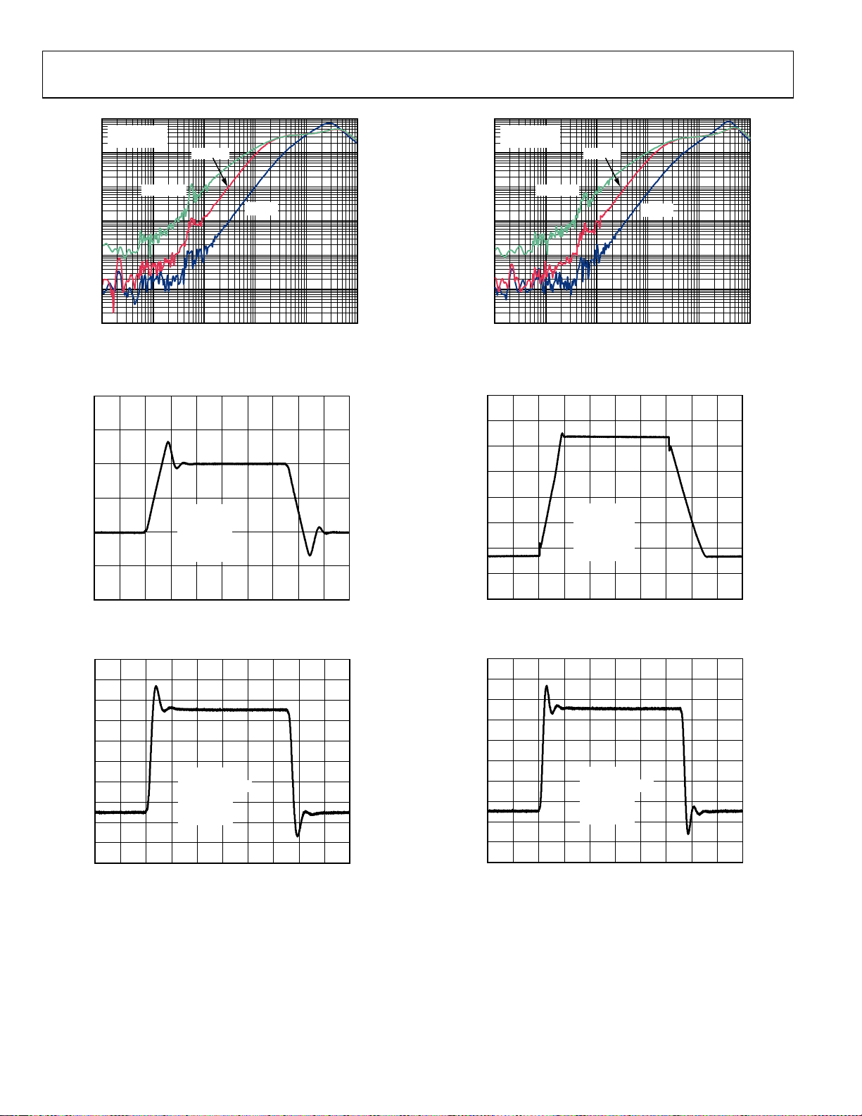
The ADA4638-1 features rail-to-rail output with a supply voltage from 4.5 V to 30 V. Figure 58 shows the input and output
waveforms of the ADA4638-1 configured as a unity-gain buffer
with a supply voltage of ±15 V and a resistive load of 10 kΩ.
The ADA4638-1 does not exhibit phase reversal.
Ф1
Ф1
Ф3
Ф4
Ф4
Ф3
Ф3
Ф3
Ф1
Ф2
Ф2
Ф1
Figure 57. ADA4638-1 Amplifier Block Diagram
A1
A2
Ф4
Ф3
Ф1
Ф1
Ф3
Ф4
Ф2
Ф1
Ф3
Ф3
Ф1
Ф2
A
CC
C1 C2
C3 C4
OUT
OUT
A3
A4
10072-157
Rev. 0 | Page 17 of 24
Page 18

ADA4638-1 Data Sheet
Ω
Ω
V
V
VSY = ±15V
RL=10kΩ
V
IN
V
OUT
VOLTAGE (10V/DIV)
TIME (2µs/DIV)
10072-158
Figure 58. No Phase Reversal
NOISE CONSIDERATIONS
1/f Noise
1/f noise, also known as pink noise or flicker noise, is inherent
in semiconductor devices and increases as frequency decreases.
At low frequency, 1/f noise is a major noise contributor and
causes a significant output voltage offset when amplified by the
noise gain of the circuit. However, the ADA4638-1 eliminates
the 1/f noise internally, thus making it an excellent choice for dc
or low frequency high precision applications. The 0.1 Hz to
10 Hz voltage noise is only 1.2 µV p-p at ±15 V of supply voltage.
The low frequency 1/f noise appears as a slow varying offset to
the ADA4638-1 and is greatly reduced by the combination of
auto-zeroing and chopping technique. This allows the ADA4638-1
to have a much lower noise at dc and low frequency in comparison
to standard low noise amplifiers that are susceptible to 1/f noise.
Figure 47 and Figure 50 show the voltage noise density of the
ADA4638-1 with no 1/f noise.
COMPARATOR OPERATION
Op amps are designed to operate in a closed-loop configuration
with feedback from its output to its inverting input. Figure 59
shows the ADA4638-1 configured as a voltage follower with an
input voltage, which is kept at midpoint of the power supplies.
A1 and A2 indicate the placement of ammeters to measure supply
currents. I
supply pin of the op amp, and I
out of the negative supply pin of the op amp. From Figure 60, as
expected in normal operating condition, the current flowing
into the op amp is equivalent to the current flowing out of the op
amp, where I
+ refers to the current flowing into the positive
SY
− refers to the current flowing
SY
+ = ISY−.
SY
+
SY
A1
ISY+
100k
100k
ADA4638-1
A2
–V
SY
ISY–
V
OUT
10072-059
Figure 59. Voltage Follower
1.0
0.8
0.6
0.4
0.2
0
–0.2
PER AMPLIFIER (mA)
–0.4
SY
I
–0.6
–0.8
–1.0
0 5 10 15 20 25 30
I
+
SY
–
I
SY
VSY (V)
10072-060
Figure 60. Supply Current vs. Supply Voltage (Voltage Follower)
In contrast to op amps, comparators are designed to work in an
open-loop configuration and to drive logic circuits. Although
op amps are different from comparators, occasionally an unused
section of a dual op amp is used as a comparator to save board
space and cost; however, this is not recommended.
Figure 61 and Figure 62 show the ADA4638-1 configured as
a comparator, with resistors R
IN1
and R
in series with the
IN2
input pins.
+
SY
A3 I
I
INPUT
R
IN1
A1 ISY+
+
ADA4638-1
TOTAL
+
V
OUT
I
R
INPUT–
IN2
A2 ISY–
A4 I
–V
SY
TOTAL
–
10072-061
Figure 61. Comparator A
Rev. 0 | Page 18 of 24
Page 19

Data Sheet ADA4638-1
I
+
INPUT
R
IN1
I
R
INPUT–
IN2
+V
SY
A1 I
A3 ISY+
ADA4638-1
A4 ISY–
A2 I
–V
SY
TOTAL
TOTAL
+
V
OUT
–
10072-062
Figure 62. Comparator B
Figure 63 and Figure 64 show the total supply current of the
system, I
out of the supply pins of the ADA4638-1. With R
, and the actual currents, ISY, that flow into and
TOTAL
IN1
= R
IN2
=
100 kΩ and supply voltage of 30 V, the total supply current of
the system is 800 µA to 900 A.
With smaller input series resistors, total supply current of the
system increases much more. Figure 65 and Figure 66 show the
supply currents with R
IN1
= R
= 0 Ω. The total current of the
IN2
system increases to 10 mA.
I
TOTAL
= ISY + I
INPUT
Note that, at 30 V of supply voltage, 8 mA to 9 mA of current
flows through the input pins. This is undesirable. The ADA4638-1
is not recommended to be used as a comparator. If absolutely
necessary, place resistors in series with the inputs of the amplifier to limit input current to less than 10 mA.
For more details on op amps as comparators, refer to the
AN-849 Application Note, Using Op Amps as Comparators.
1.0
0.8
0.6
0.4
0.2
0
–0.2
CURRENT (mA)
–0.4
–0.6
–0.8
–1.0
0 5 10 15 20 25 30
Figure 63. Supply Current vs. Supply Voltage
(Comparator A, R
I
TOTAL
ISY+
I
SY
I
TOTAL
+
–
–
VSY (V)
= R
IN1
= 100 kΩ)
IN2
10072-063
1.0
0.8
0.6
0.4
0.2
0
–0.2
CURRENT (mA)
–0.4
–0.6
–0.8
–1.0
0 5 10 15 20 25 30
I
TOTAL
ISY+
I
SY
I
TOTAL
+
–
–
VSY (V)
10072-064
Figure 64. Supply Current vs. Supply Voltage
(Comparator B, R
12
10
8
6
4
2
0
–2
CURRENT (mA)
–4
–6
–8
–10
–12
I
+
TOTAL
ISY+
I
–
SY
I
–
TOTAL
0 5 10 15 20 25 30
= R
IN1
VSY (V)
= 100 kΩ)
IN2
10072-065
Figure 65. Supply Current vs. Supply Voltage
= R
(Comparator A, R
= 0 kΩ)
IN1
IN2
12
10
8
6
4
2
0
–2
CURRENT (mA)
–4
–6
–8
–10
–12
I
+
TOTAL
ISY+
I
–
SY
I
–
TOTAL
0 5 10 15 20 25 30
VSY (V)
10072-066
Figure 66. Supply Current vs. Supply Voltage
= R
(Comparator B, R
= 0 kΩ)
IN1
IN2
Rev. 0 | Page 19 of 24
Page 20

ADA4638-1 Data Sheet
V
*V
V
PRECISION LOW-SIDE CURRENT SHUNT SENSOR
Many applications require the sensing of signals near the
positive or negative rails. Current shunt sensors are one such
application and are mostly used for feedback control systems.
They are also used in a variety of other applications, including
power metering, battery fuel gauging and feedback controls in
electrical power steering. In such application, it is desirable to
use a shunt with very low resistance to minimize series voltage
drop. This not only minimizes wasted power, but also allows the
measurement of high currents while saving power. A typical
shunt may be 100 mΩ. At a measured current of 1 A, the
voltage produced from the shunt is 100 mV, and the amplifier
error sources are not critical. However, at low measured current
in the 1 mA range, the 100 μV generated across the shunt
demands a very low offset voltage and drift amplifier to
maintain absolute accuracy. The unique attributes of a zerodrift amplifier provides a solution. The ADA4638-1, with its
input common-mode voltage that includes the lower supply rail,
can be used for implementing low-side current shunt sensors.
Figure 67 shows a low-side current sensing circuit using the
ADA4638-1. The ADA4638-1 is configured as a difference
amplifier with a gain of 1000. Although the ADA4638-1 has
high common-mode rejection, the CMR of the system is limited
by the external resistors. Therefore, the key to high CMR for the
system are resistors that are well matched from both the
resistive ratio and relative drift, where R1/R2 = R3/R4. The
resistors are important in determining the performance over
manufacturing tolerances, time, and temperature.
I
R1
100Ω
R3
100Ω
R
0.1Ω
S
S
R
L
10072-167
V
OUT
SY
*
R2
100kΩ
I
V
SY
ADA4638-1
R4
100kΩ
= AMPLIFIER GAIN × VOLTAGE ACROSS R
OUT
= 1000 × RS × I
= 100 × I
Figure 67. Low-Side Current Sensing Circuit
PRINTED CIRCUIT BOARD LAYOUT
The ADA4638-1 is a high precision device with ultralow offset
voltage and offset voltage drift. Therefore, care must be taken in
the design of the printed circuit board (PCB) layout to achieve
optimum performance of the ADA4638-1 at board level.
To avoid leakage currents, keep the surface of the board clean
and free of moisture. Coating the board surface creates a barrier
to moisture accumulation and reduces parasitic resistance on
the board.
Properly bypassing the power supplies and keeping the supply
traces short minimizes power supply disturbances caused by
output current variation. Connect bypass capacitors as close as
possible to the device supply pins. Stray capacitances are a
concern at the outputs and the inputs of the amplifier. It is
recommended that signal traces be kept at a distance of at least
5 mm from supply lines to minimize coupling.
A potential source of offset error is the Seebeck voltage on the
circuit board. The Seebeck voltage occurs at the junction of two
dissimilar metals and is a function of the temperature of the
junction. The most common metallic junctions on a circuit
board are solder-to-board trace and solder-to-component lead.
Figure 68 shows a cross section of a surface-mount component
soldered to a PCB. A variation in temperature across the board
(where T
≠ TA2) causes a mismatch in the Seebeck voltages at
A1
the solder joints thereby resulting in thermal voltage errors that
degrade the performance of the ultralow offset voltage of the
ADA4638-1.
COMPONENT
LEAD
SC1
V
SC2
SOLDER
+
V
TS2
+
T
A2
≠ V
+ V
TS2
SC2
V
SC1
TS1
COPPER
TRACE
+
+
T
A1
SURFACE-MOUNT
COMPONENT
PC BOARD
IF TA1 ≠ TA2, THEN
+ V
V
TS1
Figure 68. Mismatch in Seebeck Voltages Causes Seebeck Voltage Error
To minimize these thermocouple effects, orient resistors so that
heat sources warm both ends equally. Where possible, the input
signal paths should contain matching numbers and types of
components to match the number and type of thermocouple
junctions. For example, dummy components, such as zero value
resistors, can be used to match the thermoelectric error source
(real resistors in the opposite input path). Place matching components in close proximity and orient them in the same manner to
ensure equal Seebeck voltages, thus cancelling thermal errors.
Additionally, use leads that are of equal length to keep thermal
conduction in equilibrium. Keep heat sources on the PCB as far
away from amplifier input circuitry as is practical.
It is highly recommended to use a ground plane. A ground plane
helps distribute heat throughout the board, maintains a constant
temperature across the board, and reduces EMI noise pickup.
10072-067
Rev. 0 | Page 20 of 24
Page 21

Data Sheet ADA4638-1
OUTLINE DIMENSIONS
2.44
3.10
3.00 SQ
2.90
2.34
2.24
5
0.50 BSC
8
PIN 1 INDEX
AREA
0.80
0.75
0.70
SEATING
PLANE
COPLANARITY
EXPOSED
PAD
0.50
0.40
0.30
TOP VIEW
0.05 MAX
0.02 NOM
0.30
0.25
0.20
COMPLIANTTOJEDEC STANDARDS MO-229-WEED
COPLANARIT Y
0.203 REF
0.08
4
BOTTOM VIEW
FOR PROPER CONNECTION OF
THE EXPOSED PAD, REFER TO
THE PIN CONFIGURATION
SECTION OF THIS DATA SHEET.
Figure 69. 8-Lead Lead Frame Chip Scale Package [LFCSP_WD]
3 mm × 3 mm Body, Very Very Thin, Dual Lead
(CP-8-11)
Dimensions shown in millimeters
5.00 (0.1968)
4.80 (0.1890)
4.00 (0.1574)
3.80 (0.1497)
0.25 (0.0098)
0.10 (0.0040)
0.10
SEATING
PLANE
85
1
1.27 (0.0500)
BSC
6.20 (0.2441)
5.80 (0.2284)
4
1.75 (0.0688)
1.35 (0.0532)
0.51 (0.0201)
0.31 (0.0122)
8°
0°
0.25 (0.0098)
0.17 (0.0067)
1
0.50 (0.0196)
0.25 (0.0099)
1.27 (0.0500)
0.40 (0.0157)
1.70
1.60
1.50
N
1
I
P
R
O
T
D
C
I
A
N
I
)
5
1
.
R
0
(
01-24-2011-B
45°
CONTROLLING DIMENSIONS ARE IN MILLIMETERS; INCH DIMENSIONS
(IN PARENTHESES) ARE ROUNDED-OFF MILLIMETER EQUIVALENTS FOR
REFERENCE ONLY AND ARE NOT APPROPRIATE FOR USE IN DESIGN.
COMPLIANT TO JEDEC STANDARDS MS-012-AA
012407-A
Figure 70. 8-Lead Standard Small Outline Package [SOIC_N]
Narrow Body
(R-8)
Dimensions shown in millimeters and (inches)
ORDERING GUIDE
Model1 Temperature Range Package Description Package Option Branding
ADA4638-1ACPZ-R7 −40°C to +125°C 8-Lead Lead Frame Chip Scale Package [LFCSP_WD] CP-8-11 A2W
ADA4638-1ACPZ-RL −40°C to +125°C 8-Lead Lead Frame Chip Scale Package [LFCSP_WD] CP-8-11 A2W
ADA4638-1ARZ −40°C to +125°C 8-Lead Standard Small Outline Package [SOIC_N] R-8
ADA4638-1ARZ-R7 −40°C to +125°C 8-Lead Standard Small Outline Package [SOIC_N] R-8
ADA4638-1ARZ-RL −40°C to +125°C 8-Lead Standard Small Outline Package [SOIC_N] R-8
1
Z = RoHS Compliant Part.
Rev. 0 | Page 21 of 24
Page 22

ADA4638-1 Data Sheet
NOTES
Rev. 0 | Page 22 of 24
Page 23

Data Sheet ADA4638-1
NOTES
Rev. 0 | Page 23 of 24
Page 24

ADA4638-1 Data Sheet
NOTES
©2011 Analog Devices, Inc. All rights reserved. Trademarks and
registered trademarks are the property of their respective owners.
D10072-0-10/11(0)
Rev. 0 | Page 24 of 24
 Loading...