

Page 1
10 μA, Rail-to-Rail I/O, Zero Input
ADA4505-1/ADA4505-2/ADA4505-4
FEATURES
PSRR: 100 dB minimum
CMRR: 105 dB typical
Very low supply current: 10 μA per amplifier maximum
1.8 V to 5 V single-supply or ±0.9 V to ±2.5 V dual-supply operation
Rail-to-rail input and output
3 mV offset voltage maximum
Very low input bias current: 0.5 pA typical
APPLICATIONS
Pressure and position sensors
Remote security
Medical monitors
Battery-powered consumer equipment
Hazard detectors
GENERAL DESCRIPTION
The ADA4505-1/ADA4505-2/ADA4505-4 are single, dual, and
quad micropower amplifiers featuring rail-to-rail input and output
swings while operating from a single 1.8 V to 5 V power supply
or from dual ±0.9 V to ±2.5 V power supplies.
Employing a new circuit technology, these low cost amplifiers
offer zero input crossover distortion (excellent PSRR and CMRR
performance) and very low bias current, while operating with a
supply current of less than 10 µA per amplifier.
This combination of features makes the ADA4505-x amplifiers
ideal choices for battery-powered applications because they
minimize errors due to power supply voltage variations over the
lifetime of the battery and maintain high CMRR even for a railto-rail op amp.
Remote battery-powered sensors, handheld instrumentation
and consumer equipment, hazard detectors (for example, smoke,
fire, and gas), and patient monitors can benefit from the features
of the ADA4505-x amplifiers.
The ADA4505-x family is specified for both the industrial
temperature range (−40°C to +85°C) and the extended industrial
temperature range (−40°C to +125°C). The ADA4505-1 single
amplifier is available in a tiny 5-lead SOT-23 and a 6-ball WLCSP.
The ADA4505-2 dual amplifier is available in a standard 8-lead
MSOP and a 8-ball WLCSP. The ADA4505-4 quad amplifier is
available in a 14-lead TSSOP and a 14-ball WLCSP.
The ADA4505-x family is a member of a growing series of zero
crossover op amps offered by Analog Devices, Inc., including
the AD8505/AD8506/AD8508, which also operate from a single
1.8 V to 5 V power supply or from dual ±0.9 V to ±2.5 V power
supplies.
Rev. D
Information furnished by Analog Devices is believed to be accurate and reliable. However, no
responsibility is assumed by Analog Devices for its use, nor for any infringements of patents or other
rights of third parties that may result from its use. Specifications subject to change without notice. No
license is granted by implication or otherwise under any patent or patent rights of Analog Devices.
Trademarks and registered trademarks are the property of their respective owners.
Crossover Distortion Amplifiers
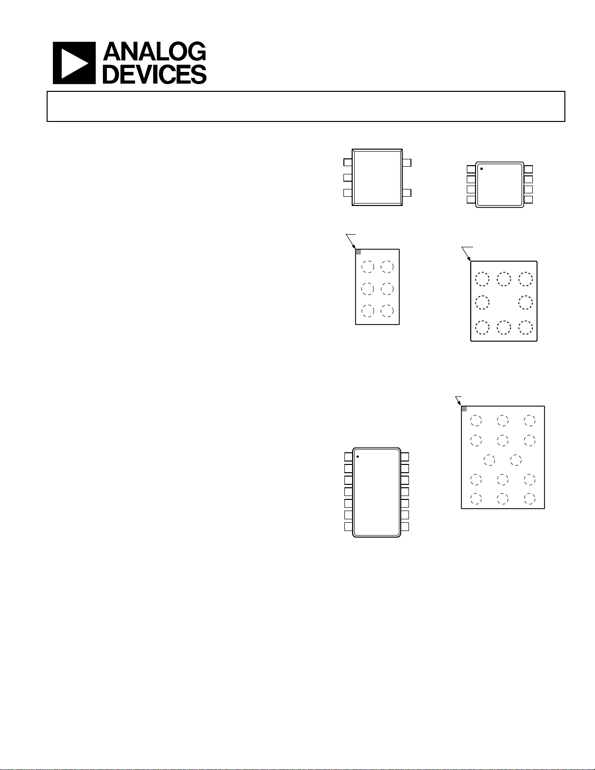
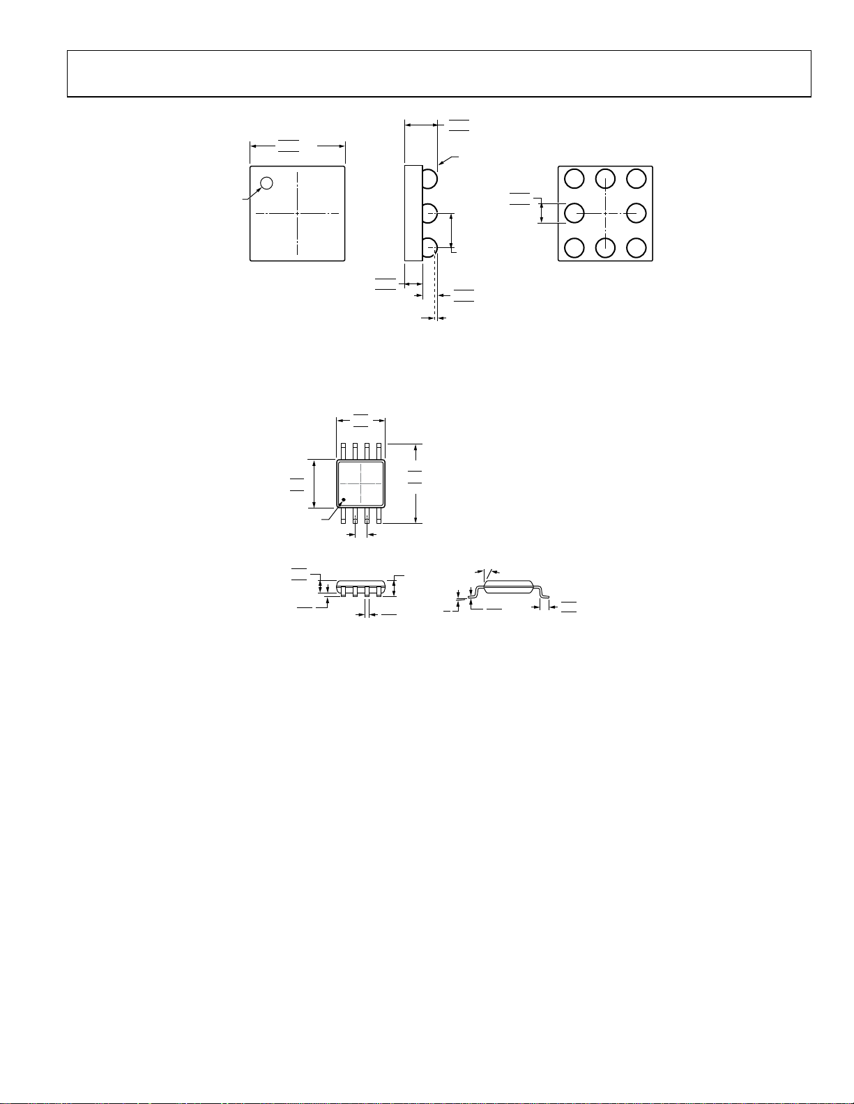
PIN CONFIGURATIONS
OUT
1
ADA4505-1
V–
2
TOP VIEW
(Not to Scal e)
+IN
3
Figure 1. 5-Lead SOT-23 (RJ-5) Figure 2. 8-Lead MSOP (RM-8)
BALL A1
INDICATOR
OUT V+
A1 A2
V–
B1 B2
+IN –IN
C1 C2
ADA4505-1
TOP VIEW
(BALL SIDE DOW N)
Not to Scal e
NC = NO CONNECT
Figure 3. 6-Ball WLCSP (CB-6-7) Figure 4. 8-Ball WLCSP (CB-8-2)
1
OUT A
2
–IN A
+IN A
+IN
–IN B
OUT B
V+
B
ADA4505-4
3
TOP VIEW
4
(Not to Scale)
5
6
7
Figure 5. 14-Lead TSSOP (RU-14) Figure 6. 14-Ball WLCSP (CB-14-1)
One Technology Way, P.O. Box 9106, Norwood, MA 02062-9106, U.S.A.
Tel: 781.329.4700 www.analog.com
Fax: 781.461.3113 ©2008–2010 Analog Devices, Inc. All rights reserved.
NC
14
13
12
11
10
5
4
9
8
V+
–IN
07416-068
OUT D
–IN D
+IN D
V–
+IN C
–IN C
OUT C
OUT A
1
ADA4505-2
2
–IN A
+IN A
07416-001
07416-005
TOP VIEW
3
(Not to Scale)
V–
4
BALL A1
CORNER
OUT B V+ OUT A
A1 A2 A3
–IN B –IN A
B1 B3
+IN B V– +IN A
C1 C2 C3
ADA4505-2
TOP VIEW
(BALL SIDE DOWN)
BALL A1
INDICATOR
OUT D OUT A –IN A
A1
–IN D V– +IN A
B1
+IN D +IN B
C1 C3
+IN C V+ –IN B
D1
–IN C OUT C OUT B
E1
ADA4505-4
TOP VIEW
(BALL SIDE DO WN)
Not to Scale
8
7
6
5
A2
A3
B2
B3
D2
D3
E2
E3
V+
OUT B
–IN B
+IN B
07416-003
07416-004
07416-061
Page 2

ADA4505-1/ADA4505-2/ADA4505-4
TABLE OF CONTENTS
Features .............................................................................................. 1
Applications ....................................................................................... 1
General Description ......................................................................... 1
Pin Configurations ........................................................................... 1
Revision History ............................................................................... 2
Specifications ..................................................................................... 3
Electrical Characteristics—1.8 V Operation ............................ 3
Electrical Characteristics—5 V Operation................................ 4
Absolute Maximum Ratings ............................................................ 5
Thermal Resistance ...................................................................... 5
REVISION HISTORY
7/10—Rev. C to Rev. D
Added 6-Ball WLCSP, ADA4505-1 .................................. Universal
Moved Electrical Characteristics—1.8 V Operation Section .... 3
Changes to Large Signal Voltage Gain Parameter, Table 1 .......... 3
Moved Electrical Characteristics—5 V Operation Section ....... 4
Changes to Large Signal Voltage Gain Parameter, Table 2 .......... 4
Changes to Thermal Resistance Section and Table 4 ................... 5
Updated Outline Dimensions ....................................................... 18
Changes to Ordering Guide .......................................................... 21
7/09—Rev. B to Rev. C
Added 5-Lead SOT-23 (ADA4505-1) ......................... Throughout
Changes to Supply Current per Amplifier Parameter, Table 1 ... 3
Changes to Supply Current per Amplifier Parameter, Table 2 ... 4
Changes to Figure 26 and Figure 29 ............................................... 9
Changes to Figure 31 and Figure 34 ............................................. 10
Changes to Figure 42 and Figure 45 ............................................. 12
Added Figure 49 and Figure 51; Renumbered Sequentially ..... 13
Updated Outline Dimensions ....................................................... 18
Changes to Ordering Guide .......................................................... 20
2/09—Rev. A to Rev. B
Added 14-Ball WLCSP (ADA4505-4) ........................ Throughout
Changes to Thermal Resistance Section ........................................ 5
Changes to Figure 17, Figure 18, Figure 20, and Figure 21 ......... 8
Changes to Figure 42 and Figure 45 ............................................. 12
Updated Outline Dimensions ....................................................... 18
Changes to Ordering Guide .......................................................... 20
ESD Caution...................................................................................5
Typical Performance Characteristics ..............................................6
Theory of Operation ...................................................................... 14
Applications Information .............................................................. 16
Pulse Oximeter Current Source ............................................... 16
Four-Pole, Low-Pass Butterworth Filter for Glucose Monitor
....................................................................................................... 17
Outline Dimensions ....................................................................... 18
Ordering Guide .......................................................................... 21
10/08—Rev. 0 to Rev. A
Added 8-Ball WLCSP (ADA4505-2) and 14-Lead TSSOP
(ADA4505-4) ................................................................. Throughout
Change to Features Section .............................................................. 1
Added Figure 2 and Figure 3; Renumbered Sequentially ............ 1
Changes to Table 1 ............................................................................. 3
Changes to Table 2 ............................................................................. 4
Changes to Thermal Resistance Section ........................................ 5
Changes to Figure 22 and Figure 25................................................ 9
Changes to Figure 40 and Figure 43............................................. 12
Deleted Figure 46 and Figure 48; Renumbered Sequentially ... 13
Change to Theory of Operation Section ..................................... 14
Changes to Figure 52 ...................................................................... 16
Change to Four-Pole Low-Pass Butterworth Filter
for Glucose Monitor Section ......................................................... 17
Updated Outline Dimensions ....................................................... 18
Changes to Ordering Guide .......................................................... 19
7/08—Revision 0: Initial Version
Rev. D | Page 2 of 24
Page 3

ADA4505-1/ADA4505-2/ADA4505-4
SPECIFICATIONS
ELECTRICAL CHARACTERISTICS—1.8 V OPERATION
VSY = 1.8 V, VCM = VSY/2, TA = 25°C, RL = 100 k to GND, unless otherwise specified.
Table 1.
Parameter Symbol Test Conditions/Comments Min Typ Max Unit
INPUT CHARACTERISTICS
Offset Voltage VOS 0 V ≤ VCM ≤ 1.8 V 0.5 3 mV
−40°C ≤ TA ≤ +125°C 4 mV
Input Bias Current IB 0.5 2 pA
−40°C ≤ TA ≤ +85°C 50 pA
−40°C ≤ TA ≤ +125°C 375 pA
Input Offset Current IOS 0.05 1 pA
−40°C ≤ TA ≤ +85°C 25 pA
−40°C ≤ TA ≤ +125°C 130 pA
Input Voltage Range −40°C ≤ TA ≤ +125°C 0 1.8 V
Common-Mode Rejection Ratio CMRR 0 V ≤ VCM ≤ 1.8 V 85 100 dB
−40°C ≤ TA ≤ +85°C 85 dB
−40°C ≤ TA ≤ +125°C 80 dB
Large Signal Voltage Gain AVO
0.05 V ≤ V
R
L
OUT
= 100 kΩ to VCM
≤ 1.75 V,
95 115 dB
−40°C ≤ TA ≤ +125°C 95 dB
Offset Voltage Drift
ΔV
OS
/ΔT
−40°C ≤ T
≤ +125°C 2.5 μV/°C
A
Input Resistance RIN 220 GΩ
Input Capacitance Differential Mode C
Input Capacitance Common Mode C
2.5 pF
INDM
4.7 pF
INCM
OUTPUT CHARACTERISTICS
Output Voltage High VOH R
= 100 kΩ to GND 1.78 1.79 V
L
−40°C ≤ TA ≤ +125°C 1.78 V
R
= 10 kΩ to GND 1.65 1.75 V
L
−40°C ≤ TA ≤ +125°C 1.65 V
Output Voltage Low VOL R
= 100 kΩ to VSY 2 5 mV
L
−40°C ≤ TA ≤ +125°C 5 mV
R
= 10 kΩ to VSY 12 25 mV
L
−40°C ≤ TA ≤ +125°C 25 mV
Short-Circuit Limit ISC V
= VSY or GND ±3.8 mA
OUT
POWER SUPPLY
Power Supply Rejection Ratio PSRR VSY = 1.8 V to 5 V 100 110 dB
−40°C ≤ TA ≤ +85°C 100 dB
−40°C ≤ TA ≤ +125°C 95 dB
Supply Current per Amplifier ISY V
= VSY/2
OUT
ADA4505-1 10 11.5 μA
–40°C ≤ TA ≤ +125°C 15 μA
ADA4505-2/ADA4505-4 7 10 μA
−40°C ≤ TA ≤ +125°C 15 μA
DYNAMIC PERFORMANCE
Slew Rate SR RL = 100 kΩ, CL = 20 pF, G = 1 6.5 mV/μs
Gain Bandwidth Product GBP RL = 1 MΩ, CL = 20 pF, G = 1 50 kHz
Phase Margin ΦM R
= 1 MΩ, CL = 20 pF, G = 1 52 Degrees
L
NOISE PERFORMANCE
Voltage Noise en p-p f = 0.1 Hz to 10 Hz 2.95 μV p-p
Voltage Noise Density en f = 1 kHz 65 nV/√Hz
Current Noise Density in f = 1 kHz 20 fA/√Hz
Rev. D | Page 3 of 24
Page 4

ADA4505-1/ADA4505-2/ADA4505-4
ELECTRICAL CHARACTERISTICS—5 V OPERATION
VSY = 5 V, VCM = VSY/2, TA = 25°C, RL = 100 k to GND, unless otherwise specified.
Table 2.
Parameter Symbol Test Conditions/Comments Min Typ Max Unit
INPUT CHARACTERISTICS
Offset Voltage VOS 0 V ≤ VCM ≤ 5 V 0.5 3 mV
−40°C ≤ TA ≤ +125°C 4 mV
Input Bias Current IB 0.5 2 pA
−40°C ≤ TA ≤ +85°C 50 pA
−40°C ≤ TA ≤ +125°C 375 pA
Input Offset Current IOS 0.05 1 pA
−40°C ≤ TA ≤ +85°C 25 pA
−40°C ≤ TA ≤ +125°C 130 pA
Input Voltage Range −40°C ≤ TA ≤ +125°C 0 5 V
Common-Mode Rejection Ratio CMRR 0 V ≤ VCM ≤ 5 V 90 105 dB
−40°C ≤ TA ≤ +85°C 90 dB
−40°C ≤ TA ≤ +125°C 85 dB
Large Signal Voltage Gain AVO
0.05 V ≤ V
R
= 100 kΩ to VCM
L
≤ 4.95 V,
OUT
−40°C ≤ TA ≤ +125°C 100 dB
Offset Voltage Drift
ΔV
OS
/ΔT
−40°C ≤ T
≤ +125°C 2 μV/°C
A
Input Resistance RIN 220 GΩ
Input Capacitance Differential Mode C
Input Capacitance Common Mode C
2.5 pF
INDM
4.7 pF
INCM
OUTPUT CHARACTERISTICS
Output Voltage High VOH R
= 100 kΩ to GND 4.98 4.99 V
L
−40°C ≤ TA ≤ +125°C 4.98 V
R
= 10 kΩ to GND 4.9 4.95 V
L
−40°C ≤ TA ≤ +125°C 4.9 V
Output Voltage Low VOL R
= 100 kΩ to VSY 2 5 mV
L
−40°C ≤ TA ≤ +125°C 5 mV
R
= 10 kΩ to VSY 10 25 mV
L
−40°C ≤ TA ≤ +125°C 25 mV
Short-Circuit Limit ISC V
= VSY or GND ±40 mA
OUT
POWER SUPPLY
Power Supply Rejection Ratio PSRR VSY = 1.8 V to 5 V 100 110 dB
−40°C ≤ TA ≤ +85°C 100 dB
−40°C ≤ TA ≤ +125°C 95 dB
Supply Current per Amplifier ISY V
= VSY/2
OUT
ADA4505-1 9 10.5 μA
–40°C ≤ TA ≤ +125°C 15 μA
ADA4505-2/ADA4505-4 7 10 μA
−40°C ≤ TA ≤ +125°C 15 μA
DYNAMIC PERFORMANCE
Slew Rate SR RL = 100 kΩ, CL = 20 pF, G = 1 6 mV/μs
Gain Bandwidth Product GBP RL = 1 MΩ, CL = 20 pF, G = 1 50 kHz
Phase Margin ΦM R
= 1 MΩ, CL = 20 pF, G = 1 52 Degrees
L
NOISE PERFORMANCE
Voltage Noise en p-p f = 0.1 Hz to 10 Hz 2.95 μV p-p
Voltage Noise Density en f = 1 kHz 65 nV/√Hz
Current Noise Density in f = 1 kHz 20 fA/√Hz
Rev. D | Page 4 of 24
105 120 dB
Page 5
ADA4505-1/ADA4505-2/ADA4505-4
ABSOLUTE MAXIMUM RATINGS
Table 3.
Parameter Rating
Supply Voltage 5.5 V
Input Voltage ±VSY ± 0.1 V
Input Current1 ±10 mA
Differential Input Voltage2 ±VSY
Output Short-Circuit Duration to GND Indefinite
Storage Temperature Range −65°C to +150°C
Operating Temperature Range −40°C to +125°C
Junction Temperature Range −65°C to +150°C
Lead Temperature (Soldering, 60 sec) 300°C
1
Input pins have clamp diodes to the supply pins. Limit input current to 10 mA
or less whenever the input signal exceeds the power supply rail by 0.1 V.
2
Diff erential input voltage is limited to 5 V or the supply voltage, whichever is less.
Stresses above those listed under Absolute Maximum Ratings
may cause permanent damage to the device. This is a stress
rating only; functional operation of the device at these or any
other conditions above those indicated in the operational
section of this specification is not implied. Exposure to absolute
maximum rating conditions for extended periods may affect
device reliability.
THERMAL RESISTANCE
θJA is specified for the worst-case conditions, that is, a device
soldered in a circuit board for surface-mount packages with its
exposed paddle soldered to a pad (if applicable). Simulated
thermal numbers on a 4-layer (2S/2P) JEDEC standard thermal
test board, unless otherwise specified.
Table 4.
Package Type θJA θJC Unit
5-Lead SOT-23 (RJ-5) 190 92 °C/W
6-Ball WLCSP (CB-6-7) 105 2.6 °C/W
8-Lead MSOP (RM-8) 142 45 °C/W
8-Ball WLCSP (CB-8-2) 82 N/A °C/W
14-Lead TSSOP (RU-14) 112 35 °C/W
14-Ball WLCSP (CB-14-1) 64 N/A °C/W
ESD CAUTION
Rev. D | Page 5 of 24
Page 6
ADA4505-1/ADA4505-2/ADA4505-4
TYPICAL PERFORMANCE CHARACTERISTICS
TA = 25°C, unless otherwise noted.
140
120
VSY = 1.8V
= VSY/2
V
CM
140
120
VSY = 5V
V
= VSY/2
CM
100
80
60
40
NUMBER OF AMPLIFIERS
20
0
–3.0 –2.5 –2.0 –1.5 –1.0 –0. 5 0 0.5 1.0 1.5 2.0 2. 5 3.0
V
(mV)
OS
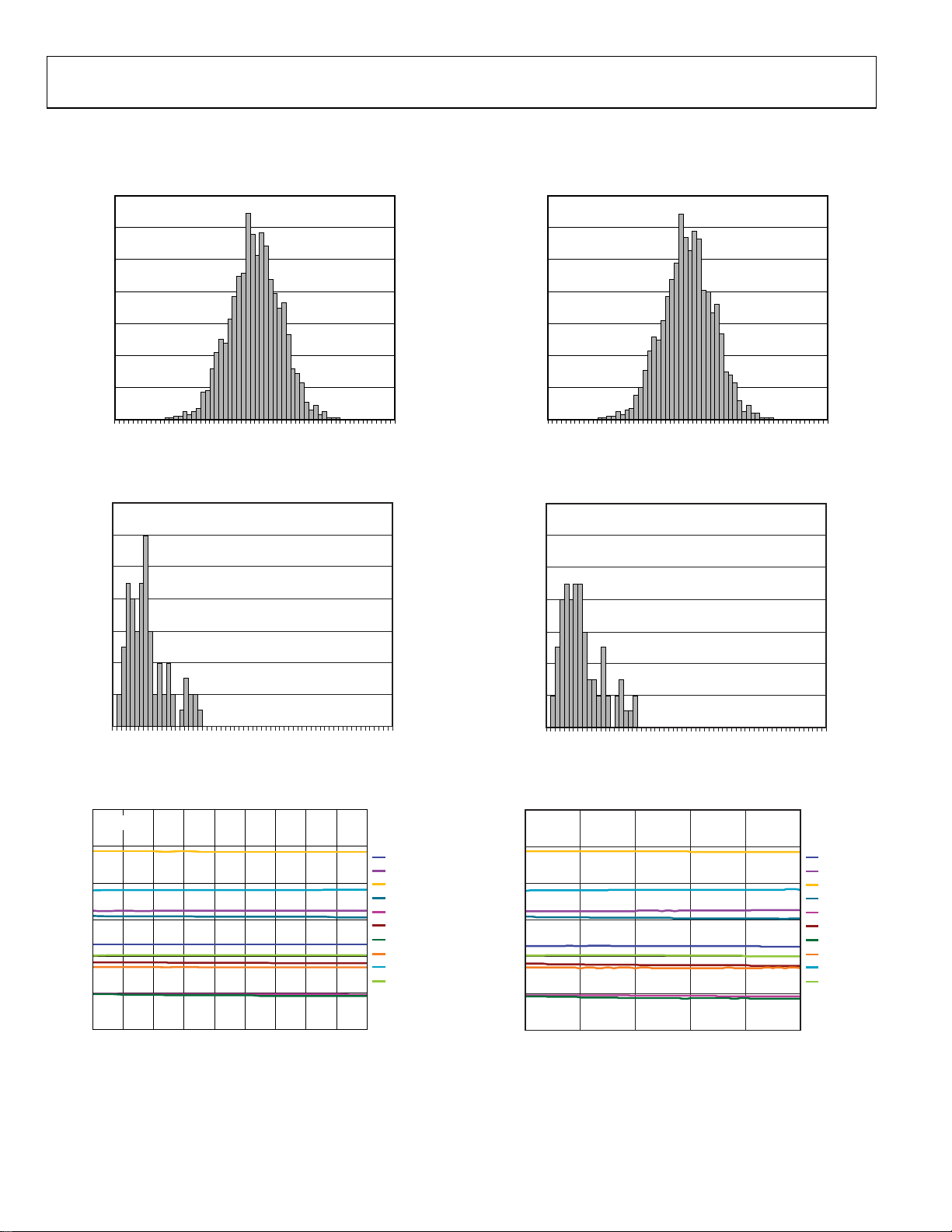
Figure 7. Input Offset Voltage Distribution
NUMBER OF AMPL IFIERS
14
12
10
8
6
4
2
VSY = 1.8V
–40°C T
A
125°C
100
80
60
40
NUMBER OF AMPLIFIERS
20
0
07416-007
–3.0 –2.5 –2.0 –1.5 –1.0 –0. 5 0 0.5 1.0 1.5 2.0 2. 5 3.0
V
(mV)
OS
07416-008
Figure 10. Input Offset Voltage Distribution
NUMBER OF AMPLIFIERS
14
12
10
8
6
4
2
VSY = 5V
–40°C T
125°C
A
0
0 0.5 1.0 1.5 2.0 2.5 3.0 3.5 4.0 4.5 5.0 5.5 6.0
TCV
OS
(µV/°C)
Figure 8. Input Offset Voltage Drift Distribution
1500
VSY = 1.8V
1000
500
(µV)
0
OS
V
–500
–1000
–1500
0 0.2 0.4 0.6 0.8 1.0 1.2 1.4 1.6 1.8
V
(V)
CM
Figure 9. Input Offset Voltage vs. Common-Mode Voltage
07416-009
DEVICE 1
DEVICE 2
DEVICE 3
DEVICE 4
DEVICE 5
DEVICE 6
DEVICE 7
DEVICE 8
DEVICE 9
DEVICE 10
07416-011
Rev. D | Page 6 of 24
0
0 0.5 1.0 1.5 2.0 2.5 3.0 3.5 4.0 4.5 5.0 5. 5 6.0
TCV
OS
(µV/°C)
Figure 11. Input Offset Voltage Drift Distribution
1500
VSY = 5V
1000
500
0
(µV)
OS
V
–500
–1000
–1500
012345
V
(V)
CM
Figure 12. Input Offset Voltage vs. Common-Mode Voltage
07416-010
DEVICE 1
DEVICE 2
DEVICE 3
DEVICE 4
DEVICE 5
DEVICE 6
DEVICE 7
DEVICE 8
DEVICE 9
DEVICE 10
07416-012
Page 7

ADA4505-1/ADA4505-2/ADA4505-4
TA = 25°C, unless otherwise noted.
1000
VSY = 1.8V
I
B+
I
B–
1000
VSY = 5V
I
B+
I
B–
100
10
(pA)
B
I
1
0.1
0 25 50 75 100 125
TEMPERATURE (° C)
Figure 13. Input Bias Current vs. Temperature
1000
100
(pA)
B
I
125°C
105°C
10
85°C
1
25°C
VSY = 1.8V
I
B+
AND I
100
10
(pA)
B
I
1
0.1
07416-013
0 25 50 75 100 125
TEMPERATURE ( °C)
07416-015
Figure 16. Input Bias Current vs. Temperature
1000
B–
125°C
100
105°C
10
(pA)
B
85°C
I
1
25°C
VSY = 5V
AND I
I
B+
B–
0.1
0 0. 2 0.4 0.6 0.8 1.0 1.2 1.4 1.6 1.8
V
(V)
CM
Figure 14. Input Bias Current vs. Common-Mode Voltage and Temperature
10k
VSY = 1.8V
1k
100
) TO SUPPLY RAIL (mV)
10
OH
1
–40°C
0.1
OUTPUT VOLTAGE (V
0.01
0.001 0.01 0.1
LOAD CURRENT (mA)
1101
+25°C
+85°C
+125°C
00
Figure 15. Output Voltage (VOH) to Supply Rail vs. Load Current
and Temperature
0.1
012 345
07416-014
V
(V)
CM
07416-016
Figure 17. Input Bias Current vs. Common-Mode Voltage and Temperature
10k
VSY = 5V
1k
100
) TO SUPPLY RAIL (mV)
10
OH
1
–40°C
0.1
OUTPUT VO LTAGE (V
0.01
0.001 0.01 0.1
07416-017
LOAD CURRENT (mA)
1101
+25°C
+85°C
+125°C
00
07416-018
Figure 18. Output Voltage (VOH) to Supply Rail vs. Load Current
and Temperature
Rev. D | Page 7 of 24
Page 8

ADA4505-1/ADA4505-2/ADA4505-4
TA = 25°C, unless otherwise noted.
10k
VSY = 1.8V
10k
VSY = 5V
1k
100
) TO SUPPLY RAIL (mV)
10
OL
1
–40°C
0.1
OUTPUT VOL TAGE (V
0.01
0.001 0.01 0.1
LOAD CURRENT (mA)
1 10 100
+25°C
+85°C
+125°C
Figure 19. Output Voltage (VOL) to Supply Rail vs. Load Current
and Temperature
1.800
RL = 100k
1.795
] (V)
OH
1.790
1.785
OUTPUT VOLTAGE [V
1.780
VSY = 1.8V
1.775
–40 –25 –10 5 20 35 50 65 80 95 110 125
RL = 10k
TEMPERATURE (° C)
Figure 20. Output Voltage (VOH) vs. Temperature
25
VSY = 1.8V
1k
100
) TO SUPPLY RAIL (mV)
10
OL
1
–40°C
0.1
OUTPUT VOL TAGE (V
0.01
07416-019
0.001 0.01 0.1
LOAD CURRENT (mA)
1 10 100
+25°C
+85°C
+125°C
07416-020
Figure 22. Output Voltage (VOL) to Supply Rail vs. Load Current
and Temperature
5.000
4.995
] (V)
4.990
OH
4.985
4.980
OUTPUT VO LTAGE [V
4.975
VSY = 5V
4.970
–40 –25 –10 5 20 35 50 65 80 95 110 125
07416-021
RL = 100k
RL = 10k
TEMPERATURE ( °C)
07416-022
Figure 23. Output Voltage (VOH) vs. Temperature
25
VSY = 5V
20
] (mV)
OL
15
10
OUTPUT VOLTAGE [V
5
0
–40 –25 –10 5 20 35 50 65 80 95 110 125
RL = 10k
RL = 100k
TEMPERATURE (° C)
Figure 21. Output Voltage (VOL) vs. Temperature
07416-023
20
] (mV)
OL
15
10
OUTPUT VO LTAGE [V
5
0
–40–25–105 203550658095110125
RL = 10k
RL = 100k
TEMPERATURE (° C)
Figure 24. Output Voltage (VOL) vs. Temperature
07416-024
Rev. D | Page 8 of 24
Page 9
ADA4505-1/ADA4505-2/ADA4505-4
TA = 25°C, unless otherwise noted.
VSY = 1.8V
225
180
135
90
45
0
–45
–90
–135
–180
–225
100
80
60
40
20
0
PHASE (Degrees)
07416-025
–20
–40
OPEN-LOOP GAIN (dB)
–60
–80
–100
100 1k 10k 100k 1M
GAIN
PHASE
FREQUENCY (Hz)
VSY = 5V
225
180
135
90
45
0
–45
–90
–135
–180
–225
PHASE (Degrees)
07416-026
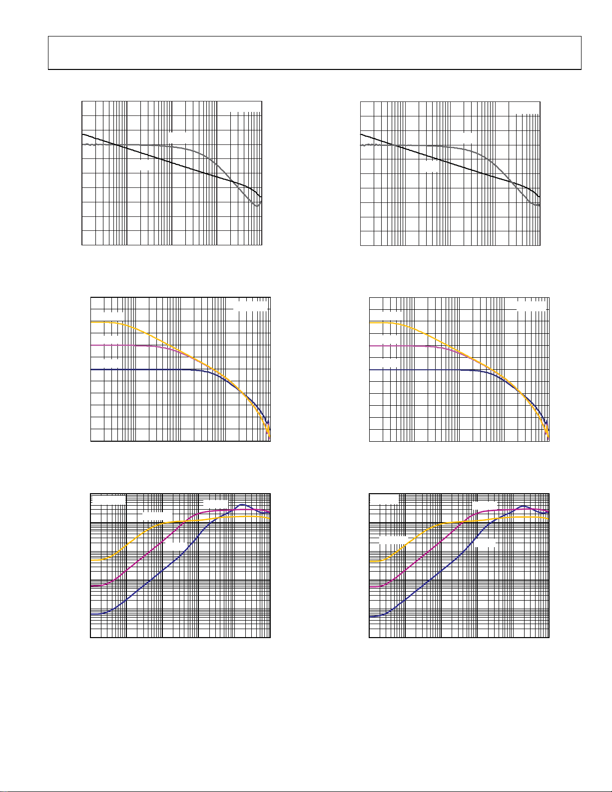
Figure 28. Open-Loop Gain and Phase vs. Frequency
60
50
G = –100
40
30
G = –10
20
10
G = –1
0
–10
–20
CLOSED-LOOP GAIN (dB)
–30
–40
–50
–60
100 1k 10k 100k 1M
07416-027
FREQUENCY (Hz)
VSY = 5V
07416-028
Figure 29. Closed-Loop Gain vs. Frequency
10k
VSY = 5V
1k
G = –10
100
80
60
40
20
0
–20
–40
OPEN-LOOP GAIN (dB)
–60
–80
–100
100 1k 10k 100k 1M
GAIN
PHASE
FREQUENCY (Hz)
VSY = 1.8V
Figure 25. Open-Loop Gain and Phase vs. Frequency
60
50
G = –100
40
30
G = –10
20
10
G = –1
0
–10
–20
CLOSED-LOOP GAIN (dB)
–30
–40
–50
–60
100 1k 10k 100k 1M
FREQUENCY (Hz)
Figure 26. Closed-Loop Gain vs. Frequency
10k
1k
VSY = 1.8V
G = –100
G = –10
100
()
OUT
Z
10
1
0.1
10 100 1k 10k 100k 1M
G = –1
FREQUENCY (Hz)
Figure 27. Output Impedance vs. Frequency
G = –100
100
()
OUT
Z
10
1
0.1
10 100 1k 10k 100k 1M
07416-062
FREQUENCY (Hz)
Figure 30. Output Impedance vs. Frequency
G = –1
07416-063
Rev. D | Page 9 of 24
Page 10

ADA4505-1/ADA4505-2/ADA4505-4
TA = 25°C, unless otherwise noted.
120
100
VSY = 1.8V
120
100
VSY = 5V
80
60
CMRR (dB)
40
20
0
100 1k 10k 100k 1M
FREQUENCY (Hz)
Figure 31. CMRR vs. Frequency
120
100
80
60
PSRR (dB)
40
20
PSRR+
PSRR–
0
10 100 1k 10k 100k 1M
FREQUENCY (Hz)
VSY = 1.8V
Figure 32. PSRR vs. Frequency
140
130
120
1.8V VSY 5V
80
60
CMRR (dB)
40
20
0
100 1k 10k 100k 1M
07416-031
FREQUENCY (Hz)
07416-032
Figure 34. CMRR vs. Frequency
120
100
80
60
PSRR (dB)
40
20
PSRR+
PSRR–
0
10 100 1k 10k 100k 1M
07416-033
FREQUENCY (Hz)
VSY = 5V
07416-034
Figure 35. PSRR vs. Frequency
1k
VSY = 5V
110
PSRR (dB)
100
90
80
–40 –25 –10 5 20 35 50 65 80 95 110 125
TEMPERATURE ( °C)
Figure 33. PSRR vs. Temperature
07416-035
100
(nV/Hz)
VSY = 1.8V
n
e
10
1 10 100 1000
FREQUENCY (Hz)
Figure 36. Voltage Noise Density vs. Frequency
07416-050
Rev. D | Page 10 of 24
Page 11

ADA4505-1/ADA4505-2/ADA4505-4
T
TA = 25°C, unless otherwise noted.
80
VSY = 1.8V
V
70
R
60
= 10mV p-p
IN
= 100k
L
80
70
60
VSY = 5V
= 10mV p-p
V
IN
= 100k
R
L
50
40
30
OVERSHOOT (%)
20
10
0
10 100 1000
CAPACITANCE (pF )
OS+
OS–
Figure 37. Small Signal Overshoot vs. Load Capacitance
T
VOLTAGE (500mV/DIV)
1.490V p-p
LOAD = 100k || 100pF
V
= 1.8V
SY
50
40
30
OVERSHOOT (%)
20
10
0
10 100 1000
07416-036
CAPACITANCE (pF )
OS+
OS–
07416-037
Figure 40. Small Signal Overshoot vs. Load Capacitance
T
3.959V p-p
VOLTAGE (1V/DIV)
LOAD = 100k || 100pF
= 5V
V
SY
T
TIME (200µs/DIV)
TIME (200µs/DIV)
LOAD = 100k || 100pF
V
= 5V
SY
07416-039
07416-041
TIME (200µs/DIV)
Figure 38. Large Signal Transient Response
T
AGE (2mV/DIV)
VOL
TIME (200µs/DIV)
Figure 39. Small Signal Transient Response
LOAD = 100k || 100pF
V
= 1.8V
SY
07416-038
Figure 41. Large Signal Transient Response
VOLTAGE (2mV/DIV)
07416-040
Figure 42. Small Signal Transient Response
Rev. D | Page 11 of 24
Page 12

ADA4505-1/ADA4505-2/ADA4505-4
TA = 25°C, unless otherwise noted.
35
40
30
25
20
(A)
SY
I
15
10
5
0
0 0.5 1.0 1.5 2.0 2.5 3.0 3.5 4.0 4.5 5.0
VSY (V)
ADA4505-4
ADA4505-2
ADA4505-1
Figure 43. Supply Current vs. Supply Voltage
VSY = 1.8V
2.95µV p-p
35
30
25
20
(A)
SY
I
15
10
5
0
–40 –25 –10 5 20 35 50 65 80 95 110 125
07416-064
ADA4505-4, VSY = 1.8V
ADA4505-4, V
ADA4505-1, VSY = 1.8V
ADA4505-1, V
= 5V
SY
TEMPERATURE (°C)
= 5V
SY
ADA4505-2, VSY = 1.8V
ADA4505-2, V
= 5V
SY
07416-065
Figure 46. Total Supply Current vs. Temperature
VSY = 5V
2.95µV p-p
INPUT VOLTAGE NOISE (0.5µV/DIV)
TIME (s)
Figure 44. Input Voltage Noise, 0.1 Hz to 10 Hz Noise
0
VSY = 1.8V
R
= 100k
L
–20
G = –100
–40
–60
–80
–100
CHANNEL SEPARATION (dB)
–120
–140
100 1k 10k 100k
100k
1k
FREQUENCY (Hz)
VIN = 0.5V p-p
V
= 1V p-p
IN
V
= 1.7V p-p
IN
Figure 45. Channel Separation vs. Frequency
07416-052
07416-057
INPUT VOLTAGE NOISE (0.5µV/DIV)
TIME (s)
Figure 47. Input Voltage Noise, 0.1 Hz to 10 Hz Noise
0
VSY = 5V
= 100k
R
L
–20
G = –100
–40
–60
–80
–100
CHANNEL SEPARATIO N (dB)
–120
–140
100 1k 10k 100k
100k
1k
FREQUENCY (Hz)
VIN = 1V p-p
= 2V p-p
V
IN
= 3V p-p
V
IN
= 4V p-p
V
IN
= 4.99V p-p
V
IN
Figure 48. Channel Separation vs. Frequency
07416-053
07416-058
Rev. D | Page 12 of 24
Page 13

ADA4505-1/ADA4505-2/ADA4505-4
2
TA = 25°C, unless otherwise noted.
1.8
1.5
VSY = 1.8V
= 1.7V
V
IN
G = 1
= 100k
R
L
6
5
VSY = 5V
V
= 4.9V
IN
G = 1
R
= 100k
L
1.2
0.9
0.6
OUTPUT SWING (V)
0.3
0
10 1 00 1k 10k 100k
FREQUENCY (Hz)
Figure 49. Output Swing vs. Frequency
VSY = ±0.9V
G = 1
= 100k
R
L
= NO LOAD
C
L
V
IN
V
OUT
4
3
2
OUTPUT SWING (V)
1
0
10 10 0 1k 10k 100k
07416-059
FREQUENCY (Hz)
07416-060
Figure 51. Output Swing vs. Frequency
VSY = ±2.5V
G = 1
= 100k
R
L
= NO LOAD
C
L
V
OUT
V
IN
1
TIME (400µs/DIV)
Figure 50. No Phase Reversal
07416-066
TIME (400µs/DIV)
Figure 52. No Phase Reversal
07416-067
Rev. D | Page 13 of 24
Page 14

ADA4505-1/ADA4505-2/ADA4505-4
V
THEORY OF OPERATION
The ADA4505-1/ADA4505-2/ADA4505-4 are unity-gain stable
CMOS rail-to-rail input/output operational amplifiers designed
to optimize performance in current consumption, PSRR, CMRR,
and zero crossover distortion, all embedded in a small package.
The typical offset voltage is 500 µV, with a low peak-to-peak
voltage noise of 2.95 µV from 0.1 Hz to 10 Hz and a voltage
noise density of 65 nV/√Hz at 1 kHz.
The ADA4505-x amplifiers are designed to solve two key
problems in low voltage battery-powered applications: battery
voltage decrease over time and rail-to-rail input stage distortion.
In battery-powered applications, the supply voltage available to
the IC is the voltage of the battery. Unfortunately, the voltage of
a battery decreases as it discharges itself through the load. This
voltage drop over the lifetime of the battery causes an error in
the output of the op amps. Some applications requiring precision
measurements during the entire lifetime of the battery use voltage
regulators to power up the op amps as a solution. If a design
uses standard battery cells, the op amps experience a supply
voltage change from roughly 3.2 V to 1.8 V during the lifetime
of the battery. This means that for a PSRR of 70 dB minimum in
a typical op amp, the input-referred offset error is approximately
440 µV. If the same application uses the ADA4505-x with a 100 dB
minimum PSRR, the error is only 14 µV. It is possible to calibrate
this error out or to use an external voltage regulator to power
the op amp, but these solutions can increase system cost and
complexity. The ADA4505-x amplifiers solve the impasse with
no additional cost or error-nullifying circuitry.
The second problem with battery-powered applications is the
distortion caused by the standard rail-to-rail input stage. Using
a CMOS nonrail-to-rail input stage (that is, a single differential
pair) limits the input voltage to approximately one V
source voltage) away from one of the supply lines. Because V
(gate-
GS
GS
for normal operation is commonly over 1 V, a single differential
pair, input stage op amp greatly restricts the allowable input
voltage range when using a low supply voltage. This limitation
restricts the number of applications where the nonrail-to-rail
input op amp was originally intended to be used. To solve this
problem, a dual differential pair input stage is usually implemented
(see Figure 53); however, this technique has its own drawbacks.
One differential pair amplifies the input signal when the commonmode voltage is on the high end, whereas the other pair amplifies
the input signal when the common-mode voltage is on the low
end. This method also requires control circuitry to operate the
two differential pairs appropriately. Unfortunately, this topology
leads to a very noticeable and undesirable problem; if the signal
level moves through the range where one input stage turns off and
the other one turns on, noticeable distortion occurs (see Figure 54).
V
IN+
Q3 Q1
I
B
V
SS
Figure 53. Typical Dual Differential Pair Input Stage Op Amp
(Dual PMOS Q1 and Q2 Transistors Form the Lower End of the Input Voltage
Range; Dual NMOS Q3 and Q4 Transistors Form the Upper End)
300
VSY = 5V
250
200
150
100
(µV)
OS
–50
V
–100
–150
–200
–250
–300
Figure 54. Typical Input Offset Voltage vs. Common-Mode Voltage
Response in a Dual Differential Pair Input Stage Op Amp (Powered by a 5 V
Supply; Results of Approximately 100 Units per Graph Are Displayed)
This distortion forces the designer to devise impractical ways
= 25°C
T
A
50
0
0
Q2
1.5 3.5 5.0
1.00.5 2.5 4.54.03.02.0
to avoid the crossover distortion areas, thereby narrowing the
common-mode dynamic range of the operational amplifier. The
ADA4505-x family solves this crossover distortion problem by
using an on-chip charge pump to power the input differential
pair. The charge pump creates a supply voltage higher than the
voltage of the battery, allowing the input stage to handle a wide
range of input signal voltages without using a second differential
pair. With this solution, the input voltage can vary from one
supply extreme to the other with no distortion, thereby restoring
the full common-mode dynamic range of the op amp.
The charge pump has been carefully designed so that switching
noise components at any frequency, both within and beyond the
amplifier bandwidth, are much lower than the thermal noise floor.
Therefore, the spurious-free dynamic range (SFDR) is limited
only by the input signal and the thermal or flicker noise. There
is no intermodulation between input signal and switching noise.
DD
Q4
VCM (V)
V
BIAS
V
IN–
I
B
07416-043
07416-044
Rev. D | Page 14 of 24
Page 15

ADA4505-1/ADA4505-2/ADA4505-4
V
V
V
V
Figure 55 displays a typical front-end section of an operational
amplifier with an on-chip charge pump.
= POSITIVE PUMPED VOLTAGE =
V
BIAS
+IN
PP
PP
Q2
Q1
–IN
V
DD
V
Figure 55. Typical Front-End Section of an Op Amp
with Embedded Charge Pump
DD
CASCODE
STAGE
AND
RAIL-TO- RAIL
OUTPUT
STAGE
SS
+ 1.8
OUT
07416-045
Figure 56 shows the typical response of two devices from Figure 12,
which shows the input offset voltage vs. input common-mode
voltage for 10 devices. Figure 56 is expanded to make it easier to
compare with Figure 54, which shows the typical input offset
voltage vs. common-mode voltage response in a dual differential
pair input stage op amp.
300
VSY = 5V
250
T
= 25°C
A
200
150
100
50
0
(µV)
OS
–50
V
–100
–150
–200
–250
–300
0
1.5 3.5 5.0
1.00.5 2.5 4.54. 03.02.0
VCM (V)
07416-046
Figure 56. Input Offset Voltage vs. Input Common-Mode Voltage Response
(Powered by a 5 V Supply; Results of Two Units Are Displayed)
This solution improves the CMRR performance tremendously.
For example, if the input varies from rail to rail on a 2.5 V
supply rail, using a part with a CMRR of 70 dB minimum,
an input-referred error of 790 µV is introduced. Another part
with a CMRR of 52 dB minimum generates a 6.3 mV error.
The ADA4505-x family CMRR of 90 dB minimum causes only
a 79 µV error. As with the PSRR error, there are complex ways
to minimize this error, but the ADA4505-x family solves this
problem without incurring unnecessary circuitry complexity or
increased cost.
Rev. D | Page 15 of 24
Page 16

ADA4505-1/ADA4505-2/ADA4505-4
V
APPLICATIONS INFORMATION
PULSE OXIMETER CURRENT SOURCE
A pulse oximeter is a noninvasive medical device used for
continuously measuring the percentage of hemoglobin (Hb)
saturated with oxygen and the pulse rate of a patient. Hemoglobin that is carrying oxygen (oxyhemoglobin) absorbs light in
the infrared (IR) region of the spectrum; hemoglobin that is not
carrying oxygen (deoxyhemoglobin) absorbs visible red (R) light.
In pulse oximetry, a clip containing two LEDs (sometimes more,
depending on the complexity of the measurement algorithm) and
the light sensor (photodiode) is placed on the finger or earlobe
of the patient. One LED emits red light (600 nm to 700 nm), and
the other emits light in the near IR (800 nm to 900 nm) region.
The clip is connected by a cable to a processor unit. The LEDs
are rapidly and sequentially excited by two current sources (one
for each LED) whose dc levels depend on the LED being driven,
based on manufacturer requirements; the detector is synchronized
to capture the light from each LED as it is transmitted through
the tissue.
An example design of a dc current source driving the red and
infrared LEDs is shown in Figure 57. These dc current sources
allow 62.5 mA and 101 mA to flow through the red and infrared
LEDs, respectively. First, to prolong battery life, the LEDs are
driven only when needed. One third of the ADG733 SPDT
analog switch is used to disconnect/connect the 1.25 V voltage
reference from/to each current circuit. When driving the LEDs,
the ADR1581 1.25 V voltage reference is buffered by one half of
the ADA4505-2; the presence of this voltage on the noninverting
input forces the output of the op amp (due to the negative feedback) to maintain a level that causes its inverting input to track
the noninverting pin. Therefore, the 1.25 V appears in parallel
with the 20 Ω R1 or 12.4 R5 current source resistor, creating
the flow of the 62.5 mA or 101 mA current through the red or
infrared LED as the output of the op amp turns on the Q1 or Q2
N-MOSFET IRLMS2002.
The maximum total quiescent currents for one half of the
ADA4505-2, the ADR1581, and the ADG733 are 15 µA, 70 µA,
and 1 µA, respectively, for a total of 86 µA current consumption
(430 µW power consumption) per circuit, which is good for a
system powered by a battery. If the accuracy and temperature
drift of the total design need improvement, use a more accurate
and low temperature coefficient drift voltage reference and current
source resistor. C3 and C4 are used to improve stabilization of U1;
R3 and R7 are used to provide some current limit into the U1
inverting pin; and R2 and R6 are used to slow the rise time of
the N-MOSFET when it turns on. These elements may not be
needed, or some bench adjustments may be required.
+5
CONNECT TO RED LED
+5V
C1
62.5mA
R2
22
Q1
IRLMS2002
R3
1k
R1
20
0.1%
1/4 W MIN
CONNECT TO I NFRARED LED
101mA
R6
22
Q2
IRLMS2002
R7
1k
R5
12.4
0.1%
1/2 W MIN
0.1µF
ADA4505-2
V
OUT1
ADA4505-2
V
OUT2
INFRARED CURRENT
8
V+
7
V–
4
C3
22pF
RED CURRENT
SOURCE
+5V
U1
1/2
8
V+
1
V–
4
C4
22pF
SOURCE
1/2
U1
C2
0.1µF
14
5
6
15
4
8
3
2
D1
D2
D3
GND
U2
ADG733
16
V
DD
S1A
S1B
S2A
S2B
S3A
S3B
A2
A1
A0
EN
V
SS
7
+5V
12
R4
53.6k
13
V
2
1
5
3
9
10
11
6
U3
ADR1581
Figure 57. Pulse Oximeter Red and Infrared Current Sources Using the
ADA4505-2 as a Buffer to the Voltage Reference Device
REF
I_BIT2
I_BIT1
I_BIT0
I_ENA
= 1.25V
07416-047
Rev. D | Page 16 of 24
Page 17

ADA4505-1/ADA4505-2/ADA4505-4
FOUR-POLE, LOW-PASS BUTTERWORTH FILTER FOR GLUCOSE MONITOR
There are several methods of glucose monitoring: spectroscopic
absorption of infrared light in the 2 µm to 2.5 µm range, reflectance spectrophotometry, and the amperometric type using
electrochemical strips with glucose oxidase enzymes. The
amperometric type generally uses three electrodes: a reference
electrode, a control electrode, and a working electrode. Although
this is a very old and widely used technique, signal-to-noise
ratio and repeatability can be improved using the ADA4505-x
family, with its low peak-to-peak voltage noise of 2.95 µV from
0.1 Hz to 10 Hz and voltage noise density of 65 nV/√Hz at 1 kHz.
C1
1000pF
R1
5M
Another consideration is operation from a 3.3 V battery. Glucose
signal currents are usually less than 3 µA full scale; therefore,
the I-to-V converter requires low input bias current. The
ADA4505-x family is an excellent choice because it provides
0.5 pA typical and 2 pA maximum input bias current at ambient
temperature.
A low-pass filter with a cutoff frequency of 80 Hz to 100 Hz is
desirable in a glucose meter device to remove extraneous noise;
this can be a simple two-pole or four-pole Butterworth filter.
Low power op amps with bandwidths of 50 kHz to 500 kHz
should be adequate. The ADA4505-x family, with its 50 kHz GBP
and 7 µA typical current consumption, meets these requirements.
A circuit design of a four-pole Butterworth filter (preceded by a
one-pole low-pass filter) is shown in Figure 58. With a 3.3 V
battery, the total power consumption of this design is 198 µW
typical at ambient temperature.
CONTROL
WORKING
REFERENCE
+3.3V
8
3
V+
V–
2
4
ADA4505-2
DUPLICATE O F CIRCUIT ABO VE
R2
22.6k
1
U1
1/2
R3
22.6k
0.047µF
C2
0.1µF
C3
+3.3V
5
6
ADA4505-2
8
V+
V–
4
1/2
U1
R4
22.6k
7
Figure 58. Four-Pole Butterworth Filter That Can Be Used in a Glucose Meter
R5
22.6k
0.047µF
C4
0.1µF
ADA4505-2
8
V+
V–
4
1/2
U2
1
V
OUT
07416-048
+3.3V
C5
3
2
Rev. D | Page 17 of 24
Page 18

ADA4505-1/ADA4505-2/ADA4505-4
0
0
OUTLINE DIMENSIONS
3.00
2.90
2.80
.15 MAX
.05 MIN
1.70
1.60
1.50
1.30
1.15
0.90
5
123
4
1.90
BSC
0.50 MAX
0.35 MIN
COMPLIANT TO JEDEC ST ANDARDS MO-178-AA
0.95 BSC
1.45 MAX
0.95 MIN
3.00
2.80
2.60
SEATING
PLANE
0.20 MAX
0.08 MIN
10°
0.55
0.20
5°
BSC
0°
0.45
0.35
121608-A
Figure 59. 5-Lead Small Outline Transistor Package [SOT-23]
(RJ-5)
Dimensions shown in millimeters
0.645
0.600
0.555
SEATING
PLANE
0.287
0.267
0.247
0.05 NOM
COPLANARITY
0.80
BSC
0.40
BSC
0.40 BSC
12
BOTTOM VIEW
(BALL SIDE UP)
A
B
C
081709-A
BALL A1
IDENTIFIER
0.945
0.905
0.865
TOP VIEW
(BALL SIDE DOWN)
1.425
1.385
1.345
0.415
0.400
0.385
0.230
0.200
0.170
Figure 60. 6-Ball Wafer Level Chip Scale Package [WLCSP]
(CB-6-7)
Dimensions shown in millimeters
Rev. D | Page 18 of 24
Page 19
ADA4505-1/ADA4505-2/ADA4505-4
1.460
1.420 SQ
1.380
BALL 1
IDENTIFIER
TOP VIEW
0.380
0.355
0.330
COPLANARITY
0.075
0.650
0.595
0.540
SEATING
PLANE
0.50
BALL PITCH
0.270
0.240
0.210
0.340
0.320
0.300
BOTTOM VIEW
(BALL SI DE UP)
123
A
B
C
011008-B
Figure 61. 8-Ball Wafer Level Chip Scale Package [WLCSP]
(CB-8-2)
Dimensions shown in millimeters
3.20
3.00
2.80
8
5
4
0.40
0.25
5.15
4.90
4.65
1.10 MAX
15° MAX
0.23
6°
0.09
0°
0.80
0.55
0.40
100709-B
3.20
3.00
2.80
PIN 1
IDENTIFIER
0.95
0.85
0.75
0.15
0.05
COPLANARITY
1
0.65 BSC
0.10
COMPLIANT TO JEDEC STANDARDS MO-187-AA
Figure 62. 8-Lead Mini Small Outline Package [MSOP]
(RM-8)
Dimensions shown in millimeters
Rev. D | Page 19 of 24
Page 20

ADA4505-1/ADA4505-2/ADA4505-4
5.10
5.00
4.90
14
4.50
4.40
4.30
1
8
6.40
BSC
7
PIN 1
0.65 BSC
1.05
1.00
0.80
0.15
0.05
COPLANARITY
0.10
0.30
0.19
COMPLIANT TO JEDEC STANDARDS MO-153-AB-1
1.20
MAX
SEATING
PLANE
0.20
0.09
8°
0°
0.60
0.45
061908-A
0.75
Figure 63. 14-Lead Thin Shrink Small Outline Package [TSSOP]
(RU-14)
Dimensions shown in millimeters
BALL 1
IDENTIFIER
1.50
1.46
1.42
3.00
2.96
2.92
0.650
0.595
0.540
SEATING
PLANE
0.340
0.320
0.300
2.00
BSC
BSC
0.50 BSC
0.50 BSC
0.50 BSC
0.25
0.25
BSC
0.25
BSC
0.25
3
2
BSC
1
A
B
C
D
E
061208-A
TOP VIEW
(BALL SIDE DOW N)
0.380
0.355
0.330
0.10 MAX
COPLANARITY
0.270
0.240
0.210
0.50
BSC
1.00
BSC
BOTTOM VIEW
(BALL SIDE UP)
Figure 64. 14-Ball Wafer Level Chip Scale Package [WLCSP]
(CB-14-1)
Dimensions shown in millimeters
Rev. D | Page 20 of 24
Page 21

ADA4505-1/ADA4505-2/ADA4505-4
ORDERING GUIDE
Model1 Temperature Range Package Description Package Option Branding
ADA4505-1ARJZ-R2 −40°C to +125°C 5-Lead SOT-23 RJ-5 A2D
ADA4505-1ARJZ-RL −40°C to +125°C 5-Lead SOT-23 RJ-5 A2D
ADA4505-1ARJZ-R7 −40°C to +125°C 5-Lead SOT-23 RJ-5 A2D
ADA4505-1ACBZ-R7 −40°C to +125°C 6-Ball WLCSP CB-6-7 A2F
ADA4505-1ACBZ-RL −40°C to +125°C 6-Ball WLCSP CB-6-7 A2F
ADA4505-2ACBZ-RL −40°C to +125°C 8-Ball WLCSP CB-8-2 A21
ADA4505-2ACBZ-R7 −40°C to +125°C 8-Ball WLCSP CB-8-2 A21
ADA4505-2ARMZ −40°C to +125°C 8-Lead MSOP RM-8 A21
ADA4505-2ARMZ-RL −40°C to +125°C 8-Lead MSOP RM-8 A21
ADA4505-4ARUZ −40°C to +125°C 14-Lead TSSOP RU-14
ADA4505-4ARUZ-RL −40°C to +125°C 14-Lead TSSOP RU-14
ADA4505-4ACBZ-RL −40°C to +125°C 14-Ball WLCSP CB-14-1 A2A
ADA4505-4ACBZ-R7 −40°C to +125°C 14-Ball WLCSP CB-14-1 A2A
1
Z = RoHS Compliant Part.
Rev. D | Page 21 of 24
Page 22

ADA4505-1/ADA4505-2/ADA4505-4
NOTES
Rev. D | Page 22 of 24
Page 23

ADA4505-1/ADA4505-2/ADA4505-4
NOTES
Rev. D | Page 23 of 24
Page 24

ADA4505-1/ADA4505-2/ADA4505-4
NOTES
©2008–2010 Analog Devices, Inc. All rights reserved. Trademarks and
registered trademarks are the property of their respective owners.
D07416-0-7/10(D)
Rev. D | Page 24 of 24
 Loading...