

Page 1

with Output Short-to-Battery Protection
ADA4432-1/ADA4433-1
Information furnished by Analog Devices is believed to be accurate and reliable. However, no
Trademarks and registered trademarks are the property of their respective owners.
Fax: 781.461.3113 ©2012 Analog Devices, Inc. All rights reserved.
IN
GND
STB
(LFCSP ONLY)ENA +V
S
×1
×2
STB
ADA4432-1
OFFSET
SD
OUT
10597-001
+IN
GND
STBENA +V
S
R
R
2R
2R
×1
STB
STB
ADA4433-1
SD
–OUT
+OUT
10597-002
–IN
×1
SD
+
–
Data Sheet
FEATURES
Qualified for automotive applications
Output overvoltage (short-to-battery) protection up to 18 V
Short-to-battery output flag for wire diagnostics
Output short-to-ground protection
Fifth-order, low-pass video filter
0.1 dB flatness to 3 MHz
−3 dB bandwidth of 10 MHz
45 dB rejection at 27 MHz
Ultralow power-down current: 13.5 µA typical
Low quiescent current
7.6 mA typical (ADA4432-1)
13.2 mA typical (ADA4433-1)
Low supply voltage: 2.6 V to 3.6 V
Small packaging
8-lead, 3 mm × 3 mm LFCSP
6-lead SOT-23 (ADA4432-1 only)
Wide operating temperature range: −40°C to +125°C
APPLICATIONS
Automotive rearview cameras
Automotive video electronic control units (ECUs)
Surveillance video systems
GENERAL DESCRIPTION
The ADA4432-1 (single-ended output) and ADA4433-1
(differential output) are fully integrated video reconstruction
filters that combine overvoltage protection (short-to-battery [STB]
protection) and short-to-ground (STG) protection on the outputs,
with excellent video specifications and low power consumption.
The combination of STB protection and robust ESD tolerance
allows the ADA4432-1 and the ADA4433-1 to provide superior
protection in the hostile automotive environment.
The ADA4432-1 is a single-ended input/single-ended output
video filter capable of driving long back-terminated cables.
The ADA4433-1 is a fully differential video filter that can be
used as a fully differential input to a differential output or as a
single-ended input to a differential output, allowing it to easily
connect to both differential and single-ended sources. It is
capable of driving twisted pair or coaxial cable with minimal
line attenuation. Differential signal processing reduces the effects
of ground noise, which can plague ground referenced systems.
The ADA4433-1 is ideal for differential signal processing (gain
and filtering) throughout the signal chain, simplifying the
conversion between single-ended and differential components.
Rev. A
responsibility is assumed by Analog Devices for its use, nor for any infringements of patents or other
rights of thi rd parties that may result from its use. Specifications subject to change with out notice. No
license is granted by implication or otherwise under any patent or patent rights of Analog Devices.
SD Video Filter Amplifiers
FUNCTIONAL BLOCK DIAGRAMS
Figure 1.
Figure 2.
The short-to-battery protection integrated into the ADA4432-1
and ADA4433-1 protects against both dc and transient
overvoltage events, caused by an accidental short to a battery
voltage up to 18 V. The Analog Devices, Inc., short-to-battery
protection eliminates the need for large output coupling capacitors
and other complicated circuits used to protect standard video
amplifiers, saving space and cost.
The ADA4432-1 and ADA4433-1 feature a high-order filter with
−3 dB cutoff frequency response at 10 MHz and 45 dB of rejection
at 27 MHz. The ADA4432-1 and ADA4433-1 feature an internally
fixed gain of 2 V/V. This makes the ADA4432-1 and ADA4433-1
ideal for SD video applications, including NTSC and PAL.
The ADA4432-1 and ADA4433-1 operate on single supplies as
low as 2.6 V and as high as 3.6 V while providing the dynamic
range required by the most demanding video systems.
The ADA4432-1 and ADA4433-1 are offered in an 8-lead, 3 mm ×
3 mm LFCSP package. The ADA4432-1 is also available in a
6-lead SOT-23 package. All are rated for operation over the
wide automotive temperature range of −40°C to +125°C.
One Technology Way, P.O. Box 9106, Norwood, MA 02062-9106, U.S.A.
Tel: 781.329.4700
www.analog.com
Page 2

ADA4432-1/ADA4433-1 Data Sheet
TABLE OF CONTENTS
Features .............................................................................................. 1
Applications ....................................................................................... 1
General Description ......................................................................... 1
Functional Block Diagrams ............................................................. 1
Revision History ............................................................................... 2
Specifications ..................................................................................... 3
ADA4432-1 Specifications .......................................................... 3
ADA4433-1 Specifications .......................................................... 4
Absolute Maximum Ratings ............................................................ 6
Thermal Resistance ...................................................................... 6
Maximum Power Dissipation ..................................................... 6
ESD Caution .................................................................................. 6
Pin Configuration and Function Descriptions ............................. 7
Typical Performance Characteristics ............................................. 9
ADA4432-1 Typical Performance Characteristics ................... 9
ADA4433-1 Typical Performance Characteristics ................. 12
Theory of Operation ...................................................................... 15
Short Circuit (Short-to-Ground) Protection .............................. 15
Overvoltage (Short-to-Battery) Protection ................................ 15
Short-to-Battery Output Flag ................................................... 15
ESD Protection ........................................................................... 16
Enable/Disable Modes (ENA Pin) ........................................... 16
Operating Supply Voltage Range.............................................. 16
Applications Information .............................................................. 17
Methods of Transmission .......................................................... 17
Printed Circuit Board (PCB) Layout ....................................... 17
Configuring the ADA4433-1 for Single-Ended Input Signals ... 18
Pin-Compatible ADA4432-1 and ADA4433-1 ...................... 19
Typical Application Circuits ..................................................... 20
Fully DC-Coupled Transmission Line .................................... 22
Low Power Considerations....................................................... 23
Outline Dimensions ....................................................................... 24
Ordering Guide .......................................................................... 25
Automotive Products ................................................................. 25
REVISION HISTORY
5/12—Rev. 0 to Rev. A
Added ADA4432-1 and 6-Lead SOT-23 ......................... Universal
Added Figure 1; Renumbered Sequentially .................................. 1
Added Table 1; Renumbered Sequentially .................................... 3
Changes to Table 2 ............................................................................ 4
Added Figure 4, Figure 5, Table 5, and Table 6 ............................. 7
Added Figure 7 to Figure 24............................................................ 9
Changes to Operating Supply Voltage Range Section ............... 16
Added Methods of Transmission Section, Pseudo Differential
Mode (Unbalanced Source Termination) Section, Figure 43,
Pseudo Differential Mode (Balanced Source Impedance)
Section and Figure 44 ..................................................................... 17
Changed Fully Differential Transmission Mode Section to Fully
Differential Mode Section ............................................................. 17
Added Pin Compatible ADA4432-1 and ADA4433-1 Section,
Example Configuration for Package-Compatible PCB Section,
and Figure 48 to Figure 51 ............................................................ 19
Added Figure 52 ............................................................................. 20
Added Figure 54 ............................................................................. 22
Added Low Power Consideration, Figure 56, and Figure 57.... 23
Updated Outline Dimensions ....................................................... 24
Changes to Ordering Guide .......................................................... 25
4/12—Revision 0: Initial Version
Rev. A | Page 2 of 28
Page 3

Data Sheet ADA4432-1/ADA4433-1
OUTPUT CHARACTERISTICS
Quiescent Current
No input signal, no load
7.6
10
mA
SPECIFICATIONS
ADA4432-1 SPECIFICATIONS
TA = 25°C, +VS = 3.3 V, RL = 150 Ω, unless otherwise specified.
Table 1.
Parameter Test Conditions/Comments Min Typ Max Unit
DYNAMIC PERFORMANCE
−3 dB Small Signal Bandwidth V
−3 dB Large Signal Bandwidth V
ADA4432-1W only: T
1 dB Flatness V
ADA4432-1W only: T
0.1 dB Flatness V
Out-of-Band Rejection f = 27 MHz, V
ADA4432-1W only: T
Differential Gain Modulated 10-step ramp, sync tip at 0 V 0.38 %
Differential Phase Modulated 10-step ramp, sync tip at 0 V 0.69 Degrees
Group Delay Variation f = 100 kHz to 5 MHz 8 ns
Pass Band Gain 5.80 6 6.24 dB
ADA4432-1W only: T
NOISE/HARMONIC PERFORMANCE
Signal-to-Noise Ratio 100% white signal, f = 100 kHz to 5 MHz 70 dB
INPUT CHARACTERISTICS
Input Voltage Range Limited by the output voltage range 0 to 1.34 0 to 1.4 0 to 1.45 V
ADA4432-1W only: T
Input Resistance >1.0 GΩ
Input Capacitance 8 pF
Input Bias Current 35 pA
= 0.2 V p-p 10.5 MHz
OUT
= 2 V p-p 9.3 10.5 MHz
OUT
to T
MIN
MAX
= 2 V p-p 8.3 9.4 MHz
OUT
to T
MIN
MAX
= 2 V p-p 3.3 MHz
OUT
= 2 V p-p 37 43 dB
OUT
to T
MIN
MAX
to T
MIN
MAX
to T
MIN
MAX
8.6 MHz
7.6 MHz
35 dB
5.57 6.44 dB
0 to 1.3 0 to 1.47 V
Output Offset Voltage VIN = 0 V 192 280 mV
ADA4432-1W only: T
MIN
to T
MAX
300 mV
Output Voltage Swing RL = 150 Ω 0.28 +VS − 0.42 V
ADA4432-1W only: T
MIN
to T
MAX
0.30 +VS − 0.45 V
Linear Output Current ±37 mA
Short-Circuit Output Current ±50 mA
SHORT-TO-BAT TERY
Overvoltage Protection Range +VS 18 V
ADA4432-1W only: T
MIN
to T
MAX
+VS 18 V
STB Output Trigger Threshold Back termination = 75 Ω 6.3 7.2 8.1 V
ADA4432-1W only: T
MIN
to T
MAX
6.0 8.4 V
Disconnect Time After the fault is applied 150 ns
Reconnect Time After the fault is removed 300 ns
POWER SUPPLY
Power Supply Range1 2.6 3.6 V
ADA4432-1W only: T
MIN
to T
MAX
13 mA
Quiescent Current, Disabled ENA = 0 V 14 20 µA
ADA4432-1W only: T
MIN
to T
MAX
25 µA
Quiescent Current, Short-to-Battery Short-to-battery fault condition: 18 V 4.6 mA
Quiescent Current, Short to Ground Short on far end of output termination (75 Ω) 47 mA
PSRR Δ+V
= ±0.3 V, f = dc −63 dB
S RIPPLE
ENABLE PIN
Input Leakage Current ENA = high/low +0.3/−14 µA
Rev. A | Page 3 of 28
Page 4

ADA4432-1/ADA4433-1 Data Sheet
ENA V
Input voltage to disable device
≤0.6 V
ADA4433-1W only: T
to T
39
dB
ADA4433-1W only: T
to T
5.71 6.28
dB
Input Resistance
Differential
800 kΩ
Parameter Test Conditions/Comments Min Typ Max Unit
LOGIC OUTPUT/INPUT LEVELS
STB V
OH
STB V
OL
ENA V
IH
IL
OPERATING TEMPERATURE RANGE −40 +125 °C
1
Recommended range for optimal performance. Exceeding this range is not recommended.
ADA4433-1 SPECIFICATIONS
TA = 25°C, +VS = 3.3 V, V
Table 2.
Parameter Test Conditions/Comments Min Typ Max Unit
DYNAMIC PERFORMANCE
−3 dB Small Signal Bandwidth V
−3 dB Large Signal Bandwidth V
ADA4433-1W only: T
1 dB Flatness V
ADA4433-1W only: T
0.1 dB Flatness V
Out-of-Band Rejection f = 27 MHz 41 45 dB
Differential Gain Modulated 10-step ramp, sync tip at 0 V 0.5 %
Differential Phase Modulated 10-step ramp, sync tip at 0 V 1.7 Degrees
Group Delay Variation f = 100 kHz to 5 MHz 8 ns
Pass Band Gain 5.89 6 6.15 dB
NOISE/HARMONIC PERFORMANCE
Signal-to-Noise Ratio 100% white signal, f = 100 kHz to 5 MHz 67 dB
INPUT CHARACTERISTICS
Input Common-Mode Voltage Range 0 to 2.1 0 to 2.2 0 to 2.3 V
ADA4433-1W only: T
= 0.5 V, RL = 150 Ω, unless otherwise specified.
−IN
V
≥ 7.2 V (fault condition) 3.3 V
OUT
V
≤ 3.1 V (normal operation) 0.02 mV
OUT
Input voltage to enable device ≥2.4 V
= 0.2 V p-p 9.9 MHz
OUT
= 2 V p-p 8.8 9.9 MHz
OUT
to T
MIN
MAX
= 2 V p-p 7.7 8.7 MHz
OUT
to T
MIN
MAX
= 2 V p-p 3 MHz
OUT
MIN
MAX
MIN
MAX
to T
MIN
MAX
8.2 MHz
7.2 MHz
0 to 2.0 0 to 2.5 V
Common mode 400 kΩ
Input Capacitance Common mode 1.8 pF
Input Bias Current 30 pA
CMRR V
OUTPUT CHARACTERISTICS
Output Offset Voltage V
ADA4433-1W only: T
Output Voltage Swing Each single-ended output, R
ADA4433-1W only: T
Linear Output Current ±29 mA
Short-Circuit Output Current ±60 mA
Output Balance Error DC to f = 100 kHz, VIN = 0.5 V p-p −50 dB
SHORT-TO-BAT TERY
Protection Range +VS 18 V
ADA4433-1W only: T
STB Output Trigger Threshold Each output back termination = 37.5 Ω 5.0 5.4 5.7 V
ADA4433-1W only: T
Disconnect Time After the fault is applied 150 ns
Reconnect Time After the fault is removed 300 ns
−IN
+IN
= V
= 0.1 V to 1.1 V −55 dB
+IN
= V
= 0 V 1.65 1.9 V
−IN
to T
MIN
MAX
= 150 Ω 0.54 +VS − 0.55 V
L, dm
to T
MIN
MAX
to T
MIN
MAX
to T
MIN
MAX
Rev. A | Page 4 of 28
1.9 V
0.6 +VS – 0.6 V
+VS 18 V
4.9 6.0 V
Page 5

Data Sheet ADA4432-1/ADA4433-1
Quiescent Current, Disabled
ENA = 0 V
13.5
22
µA
ENA V
Input voltage to disable device
≤0.6 V
Parameter Test Conditions/Comments Min Typ Max Unit
POWER SUPPLY
Power Supply Range1 2.6 3.6 V
Quiescent Current No input signal, no load 13.2 18 mA
ADA4433-1W only: T
MIN
to T
MAX
19 mA
ADA4433-1W only: T
MIN
to T
MAX
30 µA
Quiescent Current, Short-to-Battery Short-to-battery fault condition: 18 V 18 mA
Quiescent Current, Short-to-Ground Short on far end of output termination (37.5 Ω) 60 mA
PSRR Δ+V
= ±0.3 V, f = dc −80 dB
S RIPPLE
ENABLE PIN
Input Leakage Current ENA = high/low +0.3/−14 µA
LOGIC OUTPUT/INPUT LEVELS
STB V
STB V
ENA V
OH
OL
IH
IL
V
≥ 5.7 V (fault condition) 3.3 V
OUT
V
≤ 3 V (normal operation) 0.02 V
OUT
Input voltage to enable device ≥2.4 V
OPERATING TEMPERATURE RANGE −40 +125 °C
1
Recommended range for optimal performance. Exceeding this range is not recommended.
Rev. A | Page 5 of 28
Page 6

ADA4432-1/ADA4433-1 Data Sheet
0
1
2
3
4
5
–40 –20 0 20 40 60 80 100 120
MAXIMUM POWER DISSIPATION (W)
AMBIENT T E M P E RATURE (ºC)
TJ = 150°C
LFCSP
SOT-23
10597-003
ABSOLUTE MAXIMUM RATINGS
Table 3.
Parameter Rating
Supply Voltage 4 V
Output Common-Mode Voltage 22 V
Input Differential Voltage +V
S
Power Dissipation See Figure 3
Storage Temperature Range −65°C to +125°C
Operating Temperature Range −40°C to +125°C
Lead Temperature (Soldering, 10 sec) 260°C
Junction Temperature 150°C
Stresses above those listed under Absolute Maximum Ratings
may cause permanent damage to the device. This is a stress
rating only; functional operation of the device at these or any
other conditions above those indicated in the operational
section of this specification is not implied. Exposure to absolute
maximum rating conditions for extended periods may affect
device reliability.
THERMAL RESISTANCE
θJA is specified for the device soldered to a high thermal
conductivity 4-layer (2s2p) circuit board, as described in
EIA/JESD 51-7.
The power dissipated in the package (P
quiescent power dissipation and the power dissipated in the
package due to the load drive for all outputs. The quiescent
power is the voltage between the supply pins (V
quiescent current (I
). The power dissipated due to the load drive
S
depends on the particular application. For each output, the
power due to load drive is calculated by multiplying the load
current by the associated voltage drop across the device. The
power dissipated due to the loads is equal to the sum of the
power dissipations due to each individual load. RMS voltages
and currents must be used in these calculations.
Airflow increases heat dissipation, effectively reducing θ
Figure 3 shows the maximum power dissipation in the package
vs. the ambient temperature for the 6-lead SOT-23 (170°C/W)
and the 8-lead LFCSP (50°C/W) on a JEDEC standard 4-layer
board. θ
values are approximate.
JA
) is the sum of the
D
) times the
S
.
JA
Table 4.
Package Type θJA θJC Unit
6-Lead SOT-23 170 Not applicable °C/W
8-Lead LFCSP 50 5 °C/W
MAXIMUM POWER DISSIPATION
The maximum safe power dissipation in the ADA4432-1 and
ADA4433-1 packages are limited by the associated rise in
junction temperature (T
which is the glass transition temperature, the plastic changes its
properties. Exceeding a junction temperature of 150°C for an
extended time can result in changes in the silicon devices,
potentially causing failure.
) on the die. At approximately 150°C,
J
Figure 3. Maximum Power Dissipation vs.
Ambient Temperature for a 4-Layer Board
ESD CAUTION
Rev. A | Page 6 of 28
Page 7

Data Sheet ADA4432-1/ADA4433-1
5
ENA
Enable Function. Connect to +VS or float for
NOTES
1. NC = NO CONNE C T.
2. THE EXPOSED PAD CAN BE CONNECTED
TO THE GROUND P LANE.
3+V
S
4OUT
1NC
2STB
6 GND
5 NC
8 IN
7 ENA
ADA4432-1
TOP VIEW
(Not to
Scale)
10597-004
IN
1
GND
NOTES:
1. NC = NO CONNE C T.
2
NC
3
+V
S
6
ENA
5
OUT
4
ADA4432-1
TOP VIEW
(Not to S cale)
10597-005
PIN CONFIGURATION AND FUNCTION DESCRIPTIONS
Figure 4. ADA4432-1 LFCSP Pin Configuration, Top View
Table 5. ADA4432-1 LFCSP Pin Function Descriptions
Pin
Mnemonic Description
No.
1 NC No Connect. Do not connect to this pin.
2 STB Short-to-Battery Indicator Output. A logic
high indicates a short-to-battery condition,
and a logic low indicates normal operation.
3 +VS Positive Power Supply. Bypass with 0.1 µF
capacitor to GND.
4 OUT Amplifier Output.
5 NC No Connect. Do not connect to this pin.
6 GND Power Supply Ground Pin.
7 ENA Enable Function. Connect to +VS or float for
normal operation; connect to GND for
device disable.
8 IN Input.
EPAD The exposed pad can be connected to the
ground plane.
Figure 5. ADA4432-1 SOT-23 Pin Configuration, Top View
Table 6. ADA4432-1 SOT-23 Pin Function Descriptions
Pin
Mnemonic Description
No.
1 IN Input.
2 GND Power Supply Ground Pin.
3 NC No Connect. Do not connect to this pin.
4 OUT Amplifier Output.
normal operation; connect to GND for
device disable.
6 +VS Positive Power Supply. Bypass with 0.1 µF
capacitor to GND.
Rev. A | Page 7 of 28
Page 8

ADA4432-1/ADA4433-1 Data Sheet
5
−OUT
Inverting Output.
ADA4433-1
NOTES
1. THE EXPOSED
1–IN
2STB
TOP VIEW
(Not to
3+V
S
TO THE GROUND P LANE.
Scale)
4+OUT
PAD CAN BE CONNECTED
8 +IN
7 ENA
6 GND
5 –OUT
10597-006
Figure 6. ADA4433-1 LFCSP Pin Configuration, Top View
Table 7. ADA4433-1 LFCSP Pin Function Descriptions
Pin No. Mnemonic Description
1 −IN Inverting Input.
2 STB Short-to-Battery Indicator Output. A logic high indicates a short-to-battery condition, and a logic low indicates
normal operation.
3 +VS Positive Power Supply. Bypass with a 0.1 µF capacitor to GND.
4 +OUT Noninverting Output.
6 GND Ground.
7 ENA Enable Function. Connect to +VS or float for normal operation; connect to GND for device disable.
8 +IN Noninverting Input.
EPAD The exposed pad can be connected to the ground plane.
Rev. A | Page 8 of 28
Page 9

Data Sheet ADA4432-1/ADA4433-1
–66
–60
–54
–48
–42
–36
–30
–24
–18
–12
–6
0
6
12
0.1 1 10 100
GAIN (dB)
FREQUENCY (MHz)
V
OUT
= 2.0V p-p
V
OUT
= 0.2V p-p
10597-040
–66
–60
–54
–48
–42
–36
–30
–24
–18
–12
–6
0
6
12
0.1 1 10 100
GAIN (dB)
+125°C
+25°C
–40°C
FREQUENCY (MHz)
V
OUT
= 2.0V p-p
10597-041
3.0
3.5
4.0
4.5
5.0
5.5
6.0
6.5
7.0
0.1 1 10
GAIN (dB)
FREQUENCY (MHz)
R
LOAD
= 75Ω
R
LOAD
= 100Ω
R
LOAD
= 150Ω
V
OUT
= 2.0V p-p
10597-042
3.0
3.5
4.0
4.5
5.0
5.5
6.0
6.5
0.1 1 10 100
GAIN (dB)
FREQUENCY (MHz)
V
OUT
= 2.0V p-p
V
OUT
= 0.2V p-p
10597-048
3.0
3.5
4.0
4.5
5.0
5.5
6.0
6.5
0.1 1 10 100
GAIN (dB)
FREQUENCY (MHz)
V
OUT
= 2.0V p-p
+125°C
–40°C
+25°C
10597-049
10
20
30
40
50
60
70
80
90
100
0.1 1 10 100
GROUP DELAY (ns)
FREQUENCY (MHz)
10597-050
TYPICAL PERFORMANCE CHARACTERISTICS
ADA4432-1 TYPICAL PERFORMANCE CHARACTERISTICS
TA = 25°C, +VS = 3.3 V, RL = 150 Ω, unless otherwise specified.
Figure 7. Frequency Response at Various Output Amplitudes
Figure 8. Large Signal Frequency Response at Various Temperatures
Figure 10. 1 dB Flatness Response at Various Output Amplitudes
Figure 11. 1 dB Flatness Response at Various Temperatures
Figure 9. 1 dB Flatness Response at Various Load Resistances
Figure 12. Group Delay vs. Frequency
Rev. A | Page 9 of 28
Page 10

ADA4432-1/ADA4433-1 Data Sheet
–1.5
–1.0
–0.5
0
0.5
1.0
1.5
0 1 2 3 4 5 6 7 8 9 10 11
DIFFERENTIAL GAIN (%)
f = 3.58MHz
10597-043
5.95
5.96
5.97
5.98
5.99
6.00
6.01
6.02
6.03
6.04
6.05
–40 –20 0 20 40 60 80 100 120
GAIN (dB)
TEMPERATURE (°C)
10597-057
–1.0
–0.5
0
0.5
1.0
1.5
2.0
2.5
3.0
3.5
4.0
–200 0 200 400 600 800 1000 1200 1400 1600 1800
VOLTAGE (V)
TIME (ns)
V
ENA
V
OUT
10597-044
–1.5
–1.0
–0.5
0
0.5
1.0
1.5
0 1 2 3 4 5 6 7 8 9 10 11
DIFFERENTIAL PHASE (Degrees)
f = 3.58MHz
10597-051
0 0.01 0.02 0.03 0.04 0.05
0
10
20
30
40
50
60
OUTPUT OFFSET DRIFT (V)
HITS
CSP
N: 300
MEAN: 23.5
SOT-23
N: 300
MEAN: 19
10597-056
0
2
4
6
8
10
12
0 0.4 0.8 1.2 1.6 2 2.4 2.8 3.2
SUPPLY CURRENT (mA)
ENABLE VOLTAGE (V)
+125°C
+25°C
–40°C
10597-052
Figure 13. Differential Gain Plot
Figure 14. DC Pass Band Gain Drift (−40°C to +125°C)
Figure 16. Differential Phase Plot
Figure 17. Total Output Offset Voltage Drift (−40°C to +125°C)
Figure 15 Enable (ENA)/Disable Time
Figure 18. Supply Current vs. Enable Voltage at Various Temperatures
Rev. A | Page 10 of 28
Page 11

Data Sheet ADA4432-1/ADA4433-1
–1
0
1
2
3
4
5
6
7
8
9
10
11
12
13
0 200 400 600 800 1000 1200 1400 1600
VOLTAGE (V)
TIME (ns)
STB OUTP UT
V
OUT
OVER
VOLTAGE
PULSE
10597-045
TEMPERATURE (°C)
6
7
8
9
10
11
–40 –20 0 20 40 60 80 100 120
SUPPLY CURRENT (mA)
10597-046
–0.3
0.3
0.9
1.5
2.1
2.7
3.3
0 100 200 300 400 500 600 700 800 900 1000
VOLTAGE (V)
TIME (ns)
VIN = 1.0V p-p
10597-047
0
1
2
3
4
0 1 2 3 4 5 6 7 8 9 10 11 12 13 14 15 16 17 18
FLAG VOLTAGE (V)
SHORT-TO-BATTERY (V)
STB OUTP UT
TRIGGER POINT
STB OUTP UT
RESET POINT
10597-053
–60
–50
–40
–30
–20
–10
0
0.1 1 10 100
PSRR (dB)
FREQUENCY (MHz)
REFFERED TO OUTPUT
SOT-23
LFCSP
10597-054
–130
–120
–110
–100
–90
–80
–70
–60
–50
–40
0.1 1 10 100
GAIN (dB)
FREQUENCY (MHz)
10597-055
LFCSP
SOT-23
Figure 19. STB Output Flag Response Time
Figure 20. Supply Current vs. Temperature
Figure 22. STB Output Response vs. Short-to-Battery Voltage on Outputs
Figure 23. Power Supply Rejection Ratio (PSRR) vs. Frequency
Figure 21. Output Transient Response
Figure 24. Input-to-Output Off (Disabled) Isolation vs. Frequency
Rev. A | Page 11 of 28
Page 12

ADA4432-1/ADA4433-1 Data Sheet
–66
–60
–54
–48
–42
–36
–30
–24
–18
–12
–6
0
6
12
0.1 1 10 100
GAIN (dB)
FREQUENCY (MHz)
V
OUT
= 0.2V p-p
V
OUT
= 2.0V p-p
10597-007
–66
–60
–54
–48
–42
–36
–30
–24
–18
–12
–6
0
6
12
0.1 1 10 100
GAIN (dB)
FREQUENCY (MHz)
+125°C
+25°C
–40°C
10597-008
V
OUT
= 2.0V p-p
3.0
3.5
4.0
4.5
5.0
5.5
6.0
6.5
7.0
0.1 1 10
GAIN (dB)
FREQUENCY (MHz)
R
LOAD
= 75Ω
R
LOAD
= 150Ω
V
OUT
= 2.0V p-p
R
LOAD
= 100Ω
10597-009
3.0
3.5
4.0
4.5
5.0
5.5
6.0
6.5
0.1 1 10 100
GAIN (dB)
FREQUENCY (MHz)
V
OUT
= 0.2V p-p
V
OUT
= 2.0V p-p
10597-010
3.0
3.5
4.0
4.5
5.0
5.5
6.0
6.5
0.1 1 10 100
GAIN (dB)
FREQUENCY (MHz)
+125°C
+25°C
–40°C
10597-011
V
OUT
= 2.0V p-p
10
20
30
40
50
60
70
80
90
100
0.1 1 10 100
GROUP DELAY (ns)
FREQUENCY (MHz)
10597-012
ADA4433-1 TYPICAL PERFORMANCE CHARACTERISTICS
TA = 25°C, +VS = 3.3 V, V
= 0.5 V, RL = 150 Ω, unless otherwise specified.
−IN
Figure 25. Frequency Response at Various Output Amplitudes
Figure 26. Large Signal Frequency Response at Various Temperatures
Figure 28. 1 dB Flatness Response at Various Output Amplitudes
Figure 29. 1 dB Flatness Response at Various Temperatures
Figure 27. 1 dB Flatness Response at Various Load Resistances
Figure 30. Group Delay vs. Frequency
Rev. A | Page 12 of 28
Page 13

Data Sheet ADA4432-1/ADA4433-1
–1.5
–1.0
–0.5
0
0.5
1.0
1.5
0 1 2 3 4 5 6 7 8 9 10 11
DIFFERENTIAL GAIN (%)
10597-013
f = 3.58MHz
–60
–55
–50
–45
–40
–35
–30
–25
0.1 1 6
OUTPUT BALANCE (dB)
FREQUENCY (MHz)
10597-014
V
OUT
= 2.0V p-p
–1.0
–0.5
0
0.5
1.0
1.5
2.0
2.5
3.0
3.5
4.0
–200 0 200 400 600 800 1000 1200 1400 1600 1800
VOLTAGE (V)
TIME (ns)
V
ENA
+V
OUT
–V
OUT
10597-015
–1.5
–1.0
–0.5
0
0.5
1.0
1.5
0 1 2 3 4 5 6 7 8 9 10 11
DIFFERENTIAL PHASE (Degrees)
10597-016
f = 3.58MHz
–0.04 –0.02
0
OUTPUT COMMON-MODE OFFSET DRIFT (V)
NUMBER OF DEV ICES
0.02 0.04
0
10
20
30
40
50
10597-017
N = 300
0
2
4
6
8
10
12
14
16
18
0 0.4 0.8 1.2 1.6 2.0 2.4 2.8 3.2
SUPPLY CURRENT (mA)
ENABLE VOLTAGE (V)
+125°C
+25°C
–40°C
10597-018
Figure 31. Differential Gain Plot
Figure 32. Output Balance Error vs. Frequency
Figure 34. Differential Phase Plot
Figure 35. Total Output Common-Mode Offset Voltage Drift
(−40°C to +125°C)
Figure 33. Enable (ENA)/Disable Time
Figure 36. Supply Current vs. Enable Voltage at Various Temperatures
Rev. A | Page 13 of 28
Page 14

ADA4432-1/ADA4433-1 Data Sheet
13
0 200 400 600 800 1000 1200 1400 1600
VOLTAGE (V)
TIME (ns)
STB
OUTPUT
10597-019
+V
OUT
–V
OUT
OVER
VOLTAGE
PULSE
11
12
13
14
15
16
–40 –20 0 20 40 60 80 100 120
SUPPLY CURRENT (mA)
TEMPERATURE (°C)
10597-020
0.6
0.9
1.2
1.5
1.8
2.1
2.4
2.7
3.0
OUTPUT VOLTAGE (V)
TIME (ns)
10597-021
1000 200 300 400 500 600 700 800
VIN= 1.0V p-p
4
FLAG VOLTAGE (V)
–80
–70
–60
–50
–40
–30
–20
–10
0
0.1 1 10 100
PSRR (dB)
FREQUENCY (MHz)
10597-023
REFERRED TO OUTPUT
–100
–90
–80
–70
–60
–50
0.1 1 10 100
GAIN (dB)
FREQUENCY (MHz)
10597-024
12
11
10
9
8
7
6
5
4
3
2
1
0
–1
Figure 37. STB Output Flag Response Time
STB OUTP UT
RESET POINT
3
STB OUTP UT
2
1
0
0 1 2 3 4 5 6 7 8 9 10 11 12 13 14 15 16 17 18
TRIGGER POINT
SHORT-TO-BATTERY (V)
10597-022
Figure 40. STB Output Response vs. Short-to-Battery Voltage on Outputs
Figure 38. Supply Current vs. Temperature
Figure 39. Output Transient Response
Figure 41. Power Supply Rejection Ratio (PSRR) vs. Frequency
Figure 42. Input-to-Output Off (Disabled) Isolation vs. Frequency
Rev. A | Page 14 of 28
Page 15

Data Sheet ADA4432-1/ADA4433-1
THEORY OF OPERATION
The ADA4432-1 and ADA4433-1 with short-to-battery and
short-to-ground protection are designed as fifth-order, low-pass
filters with a fixed gain of 2 that is capable of driving 2 V p-p video
signals into doubly terminated video transmission lines on a single
supply as low as 2.6 V. The filter has a 1 dB flatness of 9 MHz
and provides a typical out-of-band rejection of 45 dB at 27 MHz.
The ADA4432-1 is a single-ended filter/driver that can be used
with both ac- and dc-coupled inputs and outputs, with an input
range that includes ground for use with a ground referenced
digital-to-analog converter (DAC) in a single-supply application.
To ensure accurate reproduction of ground referenced signals
without saturating the output devices, an internal offset is
added to shift the output voltage up by 200 mV.
The ADA4433-1 is a fully differential filter/driver that is also
designed for compliance with both ac- and dc-coupled inputs and
outputs. The ADA4433-1 can be driven by a differential or single-
ended source and provides a fully differential output signal that
is biased at a voltage equal to half the supply voltage (+V
/2). When
S
the device is used with a single-ended input source, bias the
inverting input, −IN, at the middle of the input voltage range
applied to the noninverting input, +IN, allowing each output
signal to swing equally around the midsupply point (see the
Configuring the ADA4433-1 for Single-Ended Input Signals
section). This is particularly important to maximize output
voltage headroom in low supply voltage applications.
SHORT CIRCUIT (SHORT-TO-GROUND) PROTECTION
Both the ADA4432-1 and ADA4433-1 include internal protection
circuits that limit the output sink or source current to 60 mA.
This short circuit protection prevents damage to the ADA4432-1
and ADA4433-1 when the output(s) are shorted to ground, to a
low impedance source, or together (in the case of the ADA4433-1)
for an extended time. In addition, in the case of the ADA4433-1,
the total sink or source current for both outputs is limited to
50 mA, which helps protect the device in the event of both outputs
being shorted to a low impedance. However, short circuit
protection does not affect the normal operation of the devices
because one output sources current, whereas the other output
sinks current when driving a differential output signal.
OVERVOLTAGE (SHORT-TO-BATTERY) PROTECTION
Both the ADA4432-1 and ADA4433-1 include internal protection
circuits to ensure that internal circuitry is not subjected to
extreme voltages or currents during an overvoltage event
applied to their outputs. A short-to-battery condition usually
consists of a voltage on the outputs that is significantly higher
than the power supply voltage of the amplifier. Duration can
vary from a short transient to a continuous fault.
Rev. A | Page 15 of 28
The ADA4432-1 and ADA4433-1 can withstand voltages of up
to 18 V on the outputs. Critical internal nodes are protected from
exposure to high voltages by circuitry that isolates the output
devices from the high voltage and limits internal currents. This
protection is available whether the device is enabled or disabled,
even when the supply voltage is removed.
The output devices are disconnected when the voltage at the
output pins exceeds the supply voltage. After the overvoltage
condition is removed, internal circuitry pulls the output voltage
back within normal operating levels. The output devices are
reconnected when the voltage at the output pins falls below the
supply voltage by about 300 mV. When the devices are used with a
doubly terminated cable, the voltage sensed at the output pins is
lower than the voltage applied to the cable by the voltage drop
across the back termination resistor. The maximum voltage drop
across the back termination resistor is limited by the short-circuit
current protection; therefore, the threshold at which the overvoltage protection responds to a voltage applied to the cable is
V
THRESH (CABLE)
= +VS + I
LIMITRT
where:
V
THRESH (CABLE)
is the voltage applied to the cable that activates the
internal isolation circuitry.
+V
is the positive supply voltage.
S
I
is the internal short-circuit current limit, typically 50 mA.
LIMIT
R
the back termination resistance.
T
If the voltage applied to the cable is lower than V
THRESH (CABLE)
, the
voltage seen at the output pins is lower than the supply voltage,
so no overvoltage condition is detected. However, the internal
circuitry is protected by the short circuit current limit; therefore,
the ADA4432-1/ADA4433-1 can withstand an indefinite duration
short to any positive voltage up to 18 V without damage.
SHORT-TO-BATTERY OUTPUT FLAG
In addition to the internal protection circuitry, the short-tobattery output flag (STB pin) indicates an overvoltage condition
on either or both output pins. The flag is present whenever the
internal overvoltage protection is active; therefore, it is available
when the device is enabled or disabled. It is not available, however,
when the supply voltage is removed, although the internal
protection is still active. The threshold at which the short-tobattery flag is activated and deactivated is the same as the
threshold for the protection circuitry.
Table 8. STB Pin Logic
STB Pin Output Device State
High (Logic 1) Overvoltage fault condition
Low (Logic 0) Normal operation
Page 16

ADA4432-1/ADA4433-1 Data Sheet
ESD PROTECTION
All pins on the ADA4432-1 and ADA4433-1 are protected with
internal ESD protection structures connected to the power supply
pins (+V
and GND). These structures provide protection during
S
the handling and manufacturing process.
The outputs (OUT for the ADA4432-1 and +OUT and −OUT
for the ADA4433-1) can be exposed to dc voltages well above the
supply voltage in an overvoltage event; therefore, conventional
ESD structure protection cannot be used. Instead, the outputs
are protected by Analog Devices proprietary ESD devices, which
allow protection and recovery from an overvoltage event while
providing ESD protection well beyond the handling and
manufacturing requirements.
The outputs of the ADA4432-1 and ADA4433-1 are ESD
protected to survive ±8 kV and ±6 kV human body model
(HBM), respectively.
ENABLE/DISABLE MODES (ENA PIN)
The power-down or enable/disable (ENA) pin is internally pulled
up to +V
pin is high, the amplifier is enabled; pulling ENA low disables
the ADA4432-1 and ADA4433-1, reducing the supply current
to a very low 13.5 µA. With no external connection, this pin
floats high, enabling the amplifier.
through a 250 kΩ resistor. When the voltage on this
S
Table 9. ENA Pin Function
ENA Pin Input Device State
High (Logic 1) Enabled
Low (Logic 0) Disabled
High-Z (Floating) Enabled
OPERATING SUPPLY VOLTAGE RANGE
The ADA4432-1 and ADA4433-1 are specified over an operating
supply voltage range of 2.6 V to 3.6 V. This range establishes the
nominal utilization voltage at which the devices perform in
conformance with their specifications. The operating supply
voltage refers to sustained voltage levels and not to a momentary
voltage excursion that can occur due to variation in the output of
the supply regulator. When the devices operate at the limits of the
operating supply voltage range (2.6 V to 3.6 V), excursions that are
outside of this range, but less than the absolute maximum, can
lead to some performance degradation; however, they do not
damage the device.
Rev. A | Page 16 of 28
Page 17
Data Sheet ADA4432-1/ADA4433-1
INN
INP
ADA4830-1
75Ω
−
+
75Ω
POSITIVE W IRE
NEGATIVE W IRE
DRIVER PCB
ADA4432-1
10597-025
INN
INP
ADA4830-1
75Ω
−
+
37.5Ω
37.5Ω
POSITIVE W IRE
NEGATIVE W IRE
DRIVER PCB
ADA4432-1
10597-026
INN
INP
ADA4830-1
75Ω
−
+
37.5Ω
37.5Ω
POSITIVE W IRE
NEGATIVE W IRE
DRIVER PCB
ADA4433-1
10597-027
APPLICATIONS INFORMATION
METHODS OF TRANSMISSION
Pseudo Differential Mode (Unbalanced Source Termination)
The ADA4432-1 can be used as a pseudo differential driver
with an unbalanced transmission line. Pseudo differential mode
uses a single conductor to carry an unbalanced data signal from
the driver to the receiver, while a second conductor is used as a
ground reference signal.
The positive conductor connects the ADA4432-1 output to the
positive input of a differential receiver, such as ADA4830-1. The
negative wire or ground conductor from the source circuitry
connects to the negative input of the receiver. Match the impedance
of the input termination at the receiver to the output termination
of the ADA4432-1 (see Figure 43).
Fully Differential Mode
The ADA4433-1 is designed to be used as a fully differential driver.
The differential outputs of the ADA4433-1 allow fully balanced
transmission using twisted or untwisted pair cable. In this
configuration, the differential output termination consists of two
source resistors, one on each output, and each equal to half the
receiver input termination. For example, in a 75 Ω system, each
output of the ADA4433-1 is back terminated with 37.5 Ω resistors
that are connected to a differential resistance of 75 Ω at the receiver.
An illustration of this arrangement is shown in Figure 45.
Figure 43. Pseudo Differential Mode
Pseudo Differential Mode (Balanced Source Impedance)
Pseudo differential signaling is typically implemented using
unbalanced source termination, as shown in Figure 43. With this
arrangement, however, common-mode signals on the positive
and negative inputs receive different attenuation due to unbalanced
termination at the source. This effectively converts some of the
common-mode signal into a differential mode signal, degrading
the overall common-mode rejection of the system. System
common-mode rejection can be improved by balancing the output
impedance of the driver, as shown in Figure 44. Splitting the source
termination resistance evenly between the hot and cold conductors
results in matched attenuation of the common-mode signals,
ensuring maximum rejection.
Figure 44. Pseudo Differential Mode with Balanced Source Impedance
Rev. A | Page 17 of 28
Figure 45. Fully Differential Mode
PRINTED CIRCUIT BOARD (PCB) LAYOUT
As with all high speed applications, attention to PCB layout is of
paramount importance. Adhere to standard high speed layout
practices when designing with the ADA4432-1 and ADA4433-1.
A solid ground plane is recommended. Place a 0.1 µF surfacemount, ceramic power supply decoupling capacitor as close as
possible to the supply pin.
Connect the GND pin(s) to the ground plane with a trace that is
as short as possible. Us e controlled impedance traces of the shortest
length possible to connect to the signal I/O pins and do not run the
traces over any voids in the ground plane. A 75 Ω impedance level
is typically used in video applications. All signal outputs of the
ADA4432-1 and AD
A4433-1 should include series termination
resistors when driving transmission lines.
When the ADA4432-1 or the ADA4433-1 receives its inputs from a
device with current outputs, the required load resistor value for
the output current is most often different from the characteristic
impedance of the signal traces. In this case, if the interconnections
are sufficiently short (less than 2 inches), the trace does not
need to be terminated in its characteristic impedance.
Page 18
ADA4432-1/ADA4433-1 Data Sheet
INPUT SIGNAL
ADA4433-1
V
+IN
V
OCM
=
1.65V
V
+OUT
V
–OUT
+
–
V
–IN
V
DIFF
(IN) = V
+IN
– V
–IN
V
DIFF
(OUT) = V
+OUT
– V
–OUT
V
OUT
= V
DIFF
(OUT) ÷ 2
V
OUT
R
2R
2.65V
0.65V
R
0V
1.0V
1V p-p
DIFFERENTIAL OUTPUT SIGNAL DIFFERENTIAL OUTPUT SIGNAL ACROS S 2R
1V p-p
10597-028
INPUT SIGNAL
ADA4433-1
V
OCM
=
1.65V
+
–
V
DIFF
(IN) = V
+IN
– V
–IN
V
DIFF
(OUT) = V
+OUT
– V
–OUT
V
OUT
= V
DIFF
(OUT) ÷ 2
V
OUT
R
2R
1.15V
2.15V
R
0V
0.5V
1.0V
1V p-p
DIFFERENTIAL OUTPUT SIGNAL DIFFERENTIAL OUTPUT SIGNAL ACROS S 2R
1V p-p
10597-029
V
+IN
V
+OUT
V
–OUT
V
–IN
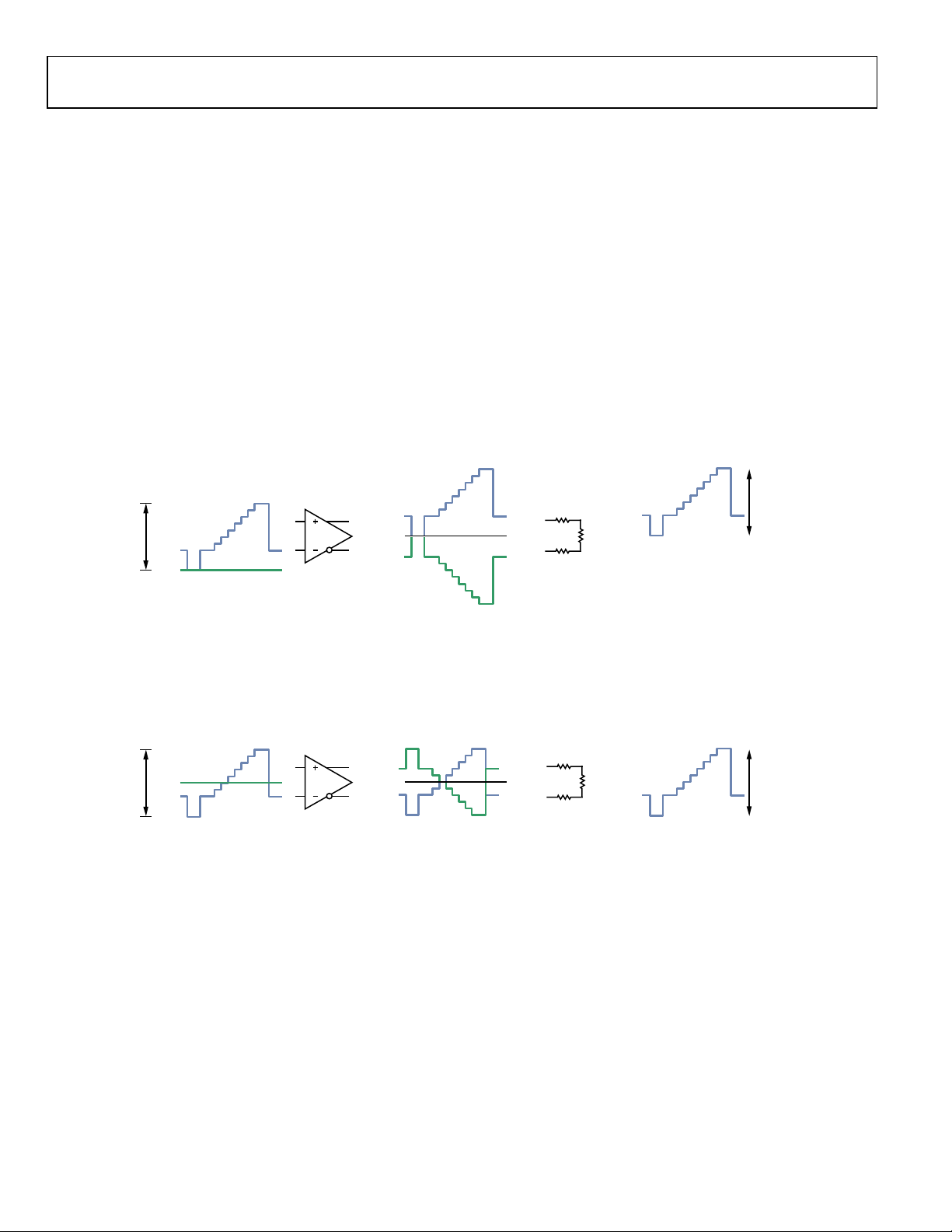
CONFIGURING THE ADA4433-1 FOR SINGLEENDED INPUT SIGNALS
The ADA4433-1 is a fully differential filter/driver that can be
used as a single-ended-to-differential amplifier or as a differentialto-differential amplifier. In single-ended-to-differential output
applications, bias the −IN input appropriately to optimize the
output range. To make the most efficient use of the output range
of the ADA4433-1, especially with low supply voltages, it is
important to allow the differential output voltage to swing in
both a positive and negative direction around the output commonmode voltage (V
differential input voltage must swing both positive and negative.
Figure 46 shows a 1 V p-p single-ended signal on +IN with −IN
grounded. This produces a differential input voltage that ranges
from 0 V to 1 V. The resulting differential output voltage is
) level, the midsupply point. To do this, the
OCM
strictly positive, where each output swings only above V
below V
, the midsupply V
−OUT
level. Directly at the output of the
OCM
ADA4433-1, the output voltage extends from 0.65 V to 2.65 V,
requiring a full 2 V of output to produce a 1 V p-p signal at the
receiver (represented by the voltage across 2R).
To make a more efficient use of the output range, the −IN input is
biased at the midpoint of the expected input signal range, as shown
in Figure 47. A 1 V p-p single-ended signal on +IN, with −IN
biased at 0.5 V, produces a differential input voltage that ranges
from −0.5 V to +0.5 V. The resulting differential output voltage
now contains both positive and negative components, where
each output swings both above and below the midsupply V
level. Directly at the output of the ADA4433-1, the output
voltage now extends only from 1.15 V to 2.15 V, requiring only
1 V of the output to produce a 1 V p-p signal at the receiver.
+OUT
or
OCM
Figure 46. Single-Ended-to-Differential Configuration with Negative Input (−IN) Connected to Ground
Figure 47. Single-Ended-to-Differential Configuration with Negative Input (−IN) Connected to 0.5 V
Rev. A | Page 18 of 28
Page 19

Data Sheet ADA4432-1/ADA4433-1
NOTES
1. NC = NO CONNE C T.
2. THE EXPOSED PAD MAY BE CONNECTED
TO THE GROUND P LANE.
3+V
S
4OUT
1NC
2STB
6 GND
5 NC
8 IN
7 ENA
ADA4432-1
TOP VIEW
10597-031
(Not to
Scale)
ENA
VIDEO
NOTES
1. THE EXPOSED PAD MAY BE CONNECTED
TO THE GROUND P LANE.
3+V
S
4+OUT
1–IN
2STB
6 GND
5 –OUT
8 +IN
7 ENA
ADA4433-1
TOP VIEW
(Not to
Scale)
10597-030
ENA
VIDEO
10597-032
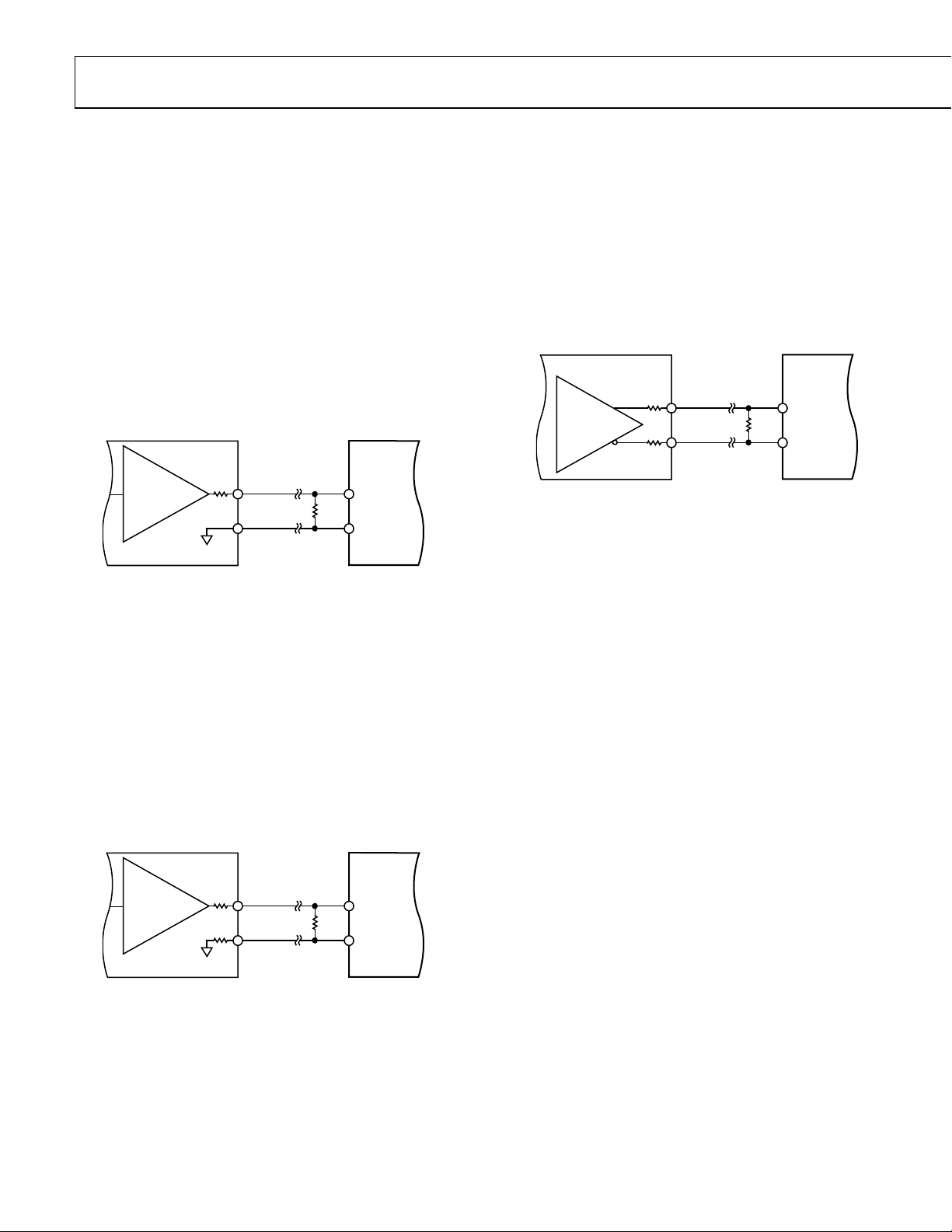
PIN-COMPATIBLE ADA4432-1 AND ADA4433-1
The ADA4432-1 and ADA4433-1 are single-ended output and
differential output, respectively, short-to-battery protected video
filters for automotive applications. Each version shares a common
package, the 8-lead LFSCP, which allows them to share a common
pinout and footprint. This allows a designer to change from a
single-ended output configuration to a differential output on
the same PCB with only minimal change to the external resistor
values and placements. Figure 48 and Figure 50 show the pin
configuration of the ADA4432-1 and ADA4433-1 in 8-lead
LFCSP packages. Figure 49 and Figure 51 show an example
schematic configured for the ADA4432-1 and the ADA4433-1,
respectively.
Example Configuration for Package-Compatible PCB
The single-ended output with the ADA4432-1 includes the following:
• R1 matches the requirement for the source.
• R2, R3, and R6 are not installed.
• C3 is not installed.
• R5 is chosen to match the receiver termination impedance.
• R8 is 0 Ω to provide ground reference.
The differential output with the ADA4433-1 includes the following:
• R1 matches the requirement for the source.
• R2 and R3 are chosen to provide the correct bias for −IN.
• C3 is for the −IN bypass.
• R5 and R6 are chosen to match the receiver termination
impedance.
• R8 is not installed.
Figure 48. 8-Lead LFCSP Package Pin Configuration, ADA4432-1
INPUT
DNI
R1
75Ω
+V
S
R3
DNI
C3
R2
DNI
Figure 49. Example Compatible Schematic Configured for the ADA4432-1
GND NCIN ENA
ADA4432-1
+VSOUTNC STB
2
1 3 4
STB
2.2µF
Figure 50. 8-Lead LFCSP Package Pin Configuration, ADA4433-1
R6
DNI
58 7 6
R8
0Ω
GROUND
REFERENCE
CONDUCTOR
INPUT
75Ω
R1
GND –OUT+IN ENA
R6
37.5Ω
58 7 6
DNI
R8
NEGATIVE
OUTPUT
CONDUCTOR
ADA4433-1
+V
S
+VS+OUT–IN STB
2
1 3 4
STB
2.2µF
R5
37.5Ω
C1
C2
0.1µF
POSITIVE
OUTPUT
CONDUCTOR
+V
S
0.1µF
R3
7.5kΩ
C3
R2
1.33kΩ
R5
75Ω
C1
C2
0.1µF
POSITIVE
OUTPUT
CONDUCTOR
+V
S
10597-033
Figure 51. Example Compatible Schematic Configured for the ADA4433-1
Rev. A | Page 19 of 28
Page 20
ADA4432-1/ADA4433-1 Data Sheet
STB
33µF 10µF
GND_IO GND_IO
0.1µF
GND_IO GND_IO
33µF 10µF
PGND PGND
0.1µF
PGND PGND
33µF 10µF
AGND AGND
0.1µF
AGND
1µF
AGND AGND
ENABLE
(INPUT) VAA
33µF 10µF
DGND DGND
0.1µF
DGND
VDD
P0
PIXEL PORT
INPUTS
P1
P2
P3
COMP
RSET
DAC1
DAC2
DAC3
ALSB
P4
P5
P6
P7
P8
P9
P10
P11 (ADV7393 ONLY)
ADV7391/
ADV7393
ADA4432-1
SOT-23 PACKAGE
P12
P13
P14
P15
HSYNC
VSYNC
CLKINCLOCK INPUT
SDA
SCL
EXTERNAL LOOP
FILTER
(OPTIONAL)
AGND PGND DGND DGND GND_IO
AGND PGND DGND DGND GND_IO
150nF
12nF
170Ω
4.12kΩ
75Ω
75Ω
TWISTED
PAIR
300Ω
AGND
DGND
AGND
2.2nF
IN
GND
VOUT
AGND
VDD
VAA
PVDD
VDD_IO
DGND
PIXEL PORT
INPUTS
I2C PORT
PVDD
10597-035
2.2µF
AGND
ENA
+V
S
0.1µF
AGND
100nF
100nF
100nF
VDD_IO
PVDD
VAA
VDD
RESET
EXT_LF
100nF
STB
STB FLAG
(OUTPUT)
CONTROL
INPUTS/OUTPUTS
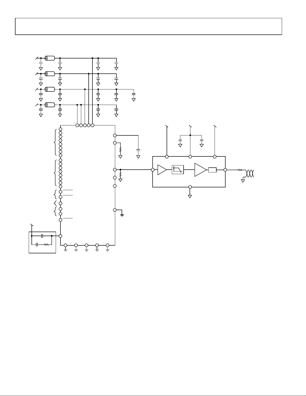
TYPICAL APPLICATION CIRCUITS
Figure 52. ADA4432-1 and ADV7391/ADV7393 Video Encoder Application Circuit
Rev. A | Page 20 of 28
Page 21
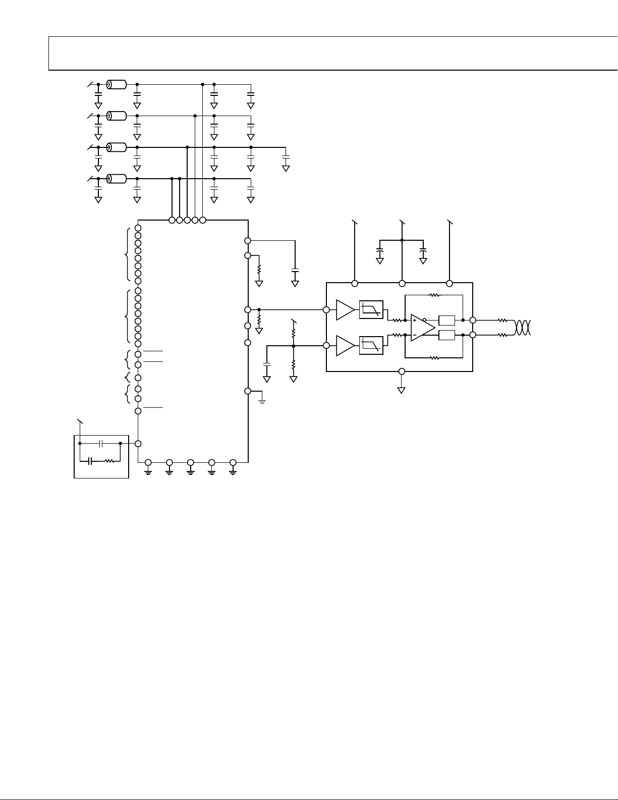
Data Sheet ADA4432-1/ADA4433-1
STB
STB
STB
33µF 10µF
GND_IO GND_IO
0.1µF
GND_IO
100nF
GND_IO
33µF 10µF
PGND PGND
0.1µF
PGND
100nF
PGND
33µF 10µF
0.1µF
AGND AGND
0.1µF
AGND
100nF 1µF
AGND AGND
ENABLE
(INPUT)
STB FLAG
(OUTPUT)VAA
33µF
VDD_IO
PVDD
VAA
VDD
10µF
DGND DGND
0.1µF
2.2µF
AGND
ENA +V
S
0.1µF
AGND
DGND
VDD
P0
PIXEL PORT
INPUTS
P1
P2
P3
COMP
R
SET
DAC 1
DAC 2
DAC 3
ALSB
P4
P5
P6
P7
P8
P9
P10
P11 (ADV7393 ONLY)
ADV7391/
ADV7393
ADA4433-1
P12
P13
P14
P15
HSYNC
VSYNC
CLKINCLOCK INPUT
SDA
SCL
RESET
EXTERNAL LOOP
FILTER
(OPTIONAL)
EXT_LF
AGND PGND DGND DGND GND_IO
AGND PGND DGND DGND GND_IO
150nF
12nF
170Ω
4.12kΩ
7.5kΩ
37.5Ω
37.5Ω
75Ω
TWISTED
PAIR
1.33kΩ
300Ω
AGND
DGND
AGND
AGND
2.2nF
+IN
–IN
GND
+OUT
–OUT
AGND
VDD
V
AA
PV
DD
V
DD_IO
100nF
DGND
PIXEL PORT
INPUTS
CONTROL
INPUTS/OUTPUTS
I2C PORT
PVDD
VAA
10597-034
Figure 53. ADA4433-1 and ADV7391/ADV7393 Video Encoder Application Circuit
Rev. A | Page 21 of 28
Page 22

ADA4432-1/ADA4433-1 Data Sheet
OR VIDEO
ENCODER
STB FLAG
+V
10597-037
INN
VOUT
TO
VIDEO
DECODER
GND
INP
ADA4830-1
ADA4433-1
75Ω
−
+
+
STBENA +VS
4.7µF
0.1µF
+VS
ENABLE
(INPUT)
STB FLAG
(OUTPUT)
2.2µF
0.1µF
4.99kΩ
+V
S
(5.0V)
VREF
−
+
75Ω
TWISTED
PAIR
R
T
+V
S
GND
LPF
LPF
+
STBENA +V
S
ENABLE
(INPUT)
STB FLAG
(OUTPUT)
2.2µF
0.1µF
0.1µF
+V
S
(3.3V)
+IN
–IN
–OUT
+OUT
37.5Ω
1.33kΩ
7.5kΩ
37.5Ω
FROM
IMAGER
OR VIDEO
ENCODER
10597-036
FULLY DC-COUPLED TRANSMISSION LINE
The ADA4432-1and ADA4433-1 are designed to be used with
high common-mode rejection, high input impedance receivers
such as the ADA4830-1, ADA4830-2, or other generic receivers.
The very low output impedance of the ADA4432-1 and the
ADA4433-1 allow them to be used in fully dc-coupled transmission
line applications in which there may be a significant discrepancy
between voltage levels at the ground pins of the driver and
receiver. As long as the voltage difference between reference
ENABLE
(INPUT)
2.2µF
+V
(3.3V)
S
STB FLAG
(OUTPUT)
0.1µF
levels at the transmitter and receiver is within the common-mode
range of the receiver, very little current flow results, and no image
degradation is anticipated.
Figure 54 and Figure 55 show an example configuration of a
completely dc-coupled transmission using the ADA4432-1 and
the ADA4433-1 along with a high input impedance differential
receiver.
S
ENABLE
(INPUT)
+VS
2.2µF
(5.0V)
+
(OUTPUT)
4.99kΩ
0.1µF
STBENA +VS
IMAGER
FROM
IN
R
T
ENA +V
S
ADA4432-1 LFCSP PACKAGE
GND
Figure 54. ADA4432-1 Video Filter and the ADA4830-1 Difference Amplifier in a DC-Coupled Configuration
Figure 55. ADA4433-1 Video Filter and ADA4830-1 Difference Amplifier in a DC-Coupled Configuration
VREF
4.7µF
75Ω
INP
INN
VOUT
0.1µF
TO VIDEO
DECODER
+
−
STB
STB
OUT
75Ω
TWISTED
−
+
75Ω
PAIR
ADA4830-1
GND
Rev. A | Page 22 of 28
Page 23

Data Sheet ADA4432-1/ADA4433-1
75Ω CABLE
75Ω
ADV7391
510Ω
3.3V
R
SET
75Ω
10597-038
300Ω
75Ω
75Ω
75Ω CABLE
ADV7391
4.12kΩ
3.3V
3.3V
R
SET
10597-039
ADA4432-1
LOW POWER CONSIDERATIONS
Using a series source termination and a shunt load termination on
a low supply voltage with the ADA4432-1 or ADA4433-1 realizes
significant power savings compared with driving a video cable
directly from a DAC output. Figure 56 shows a video DAC
driving a cable directly. Properly terminated, a DAC driven
transmission line requires two 75 Ω loads in parallel, demanding
in excess of 33 mA to reach a full-scale voltage level of 1.3 V.
Figure 57 shows the same video load being driven using the
ADA4432-1 and a series-shunt termination. This requires two
times the output voltage to drive the equivalent of 150 Ω but
only requires a little more than 15 mA to reach a full-scale output.
When running on the same supply voltage as the DAC, this result
in a 74% reduction in power consumption compared with the
circuit in Figure 56. The high order filtering provided by the
ADA4432-1 lowers the requirements on the DAC oversampling
ratio, realizing further power savings. The main source for power
savings realized by the configuration shown in Figure 57 comes
from the low drive mode setting for the ADV7391. This along
with the reduction in the requirement for oversampling (PLL
turned off), and the reduced load current required, results in
significant power savings.
For more detailed information on low drive mode, see the
ADV7391 data sheet.
Figure 56. Driving a Video Transmission Line Directly with a DAC
Figure 57. Driving a Video Transmission Line with the ADA4432-1
Rev. A | Page 23 of 28
Page 24

ADA4432-1/ADA4433-1 Data Sheet
2.44
P
TO
JEDEC STANDARDS MO-229-WEED
01-24-2011-B
COMPLIANT TO JEDEC STANDARDS MO-178-AB
10°
4°
0°
SEATING
PLANE
1.90
BSC
0.95 BSC
0.60
BSC
6 5
1 2 3
4
3.00
2.90
2.80
3.00
2.80
2.60
1.70
1.60
1.50
1.30
1.15
0.90
0.15 MAX
0.05 MIN
1.45 MAX
0.95 MIN
0.20 MAX
0.08 MIN
0.50 MAX
0.30 MIN
0.55
0.45
0.35
PIN 1
INDICATOR
12-16-2008-A
OUTLINE DIMENSIONS
2.34
2.24
5
EXPOSED
PAD
4
BOTTOM VIEW
FOR PROPER CONNECTION OF
THE EXPOSED PAD, REFER TO
THE PIN CONFIGURATION AND
FUNCTION DESCRIPTIONS
SECTION OF THIS DATA SHEET.
0.50 BSC
8
1
1.70
1.60
1.50
PIN 1
INDICATOR
(R 0.15)
IN 1 INDEX
AREA
0.80
0.75
0.70
SEATING
PLANE
3.10
3.00 SQ
2.90
TOP VIEW
0.30
0.25
0.20
COMPLIANT
0.50
0.40
0.30
0.05 MAX
0.02 NOM
COPLANARITY
0.203 REF
0.08
Figure 58. 8-Lead Lead Frame Chip Scale Package [LFCSP_WD]
3 mm × 3 mm Body, Very Very Thin, Dual Lead
(CP-8-11)
Dimensions shown in millimeters
Figure 59. 6-Lead Small Outline Transistor Package [SOT-23]
(RJ-6)
Dimensions shown in millimeters
Rev. A | Page 24 of 28
Page 25

Data Sheet ADA4432-1/ADA4433-1
ORDERING GUIDE
1, 2
Model
ADA4432-1BRJZ-R2 −40°C to +125°C 6-Lead Small Outline Transistor Package [SOT-23] RJ-6 322 250
ADA4432-1BRJZ-R7 −40°C to +125°C 6-Lead Small Outline Transistor Package [SOT-23] RJ-6 322 3000
ADA4432-1WBRJZ-R7 −40°C to +125°C 6-Lead Small Outline Transistor Package [SOT-23] RJ-6 323 3000
ADA4432-1BRJ-EBZ SOT-23 Evaluation Board
ADA4432-1BCPZ-R2 −40°C to +125°C 8-Lead Lead Frame Chip Scale Package [LFCSP_WD] CP-8-11 321 250
ADA4432-1BCPZ-R7 −40°C to +125°C 8-Lead Lead Frame Chip Scale Package [LFCSP_WD] CP-8-11 321 1500
ADA4432-1WBCPZ-R7 −40°C to +125°C 8-Lead Lead Frame Chip Scale Package [LFCSP_WD] CP-8-11 H33 1500
ADA4432-1BCP-EBZ LFCSP_WD Evaluation Board
ADA4433-1BCPZ-R2 −40°C to +125°C 8-Lead Lead Frame Chip Scale Package [LFCSP_WD] CP-8-11 331 250
ADA4433-1BCPZ-R7 −40°C to +125°C 8-Lead Lead Frame Chip Scale Package [LFCSP_WD] CP-8-11 331 1500
ADA4433-1WBCPZ-R7 −40°C to +125°C 8-Lead Lead Frame Chip Scale Package [LFCSP_WD] CP-8-11 H2Z 1500
ADA4433-1BCP-EBZ Evaluation Board
1
Z = RoHS Compliant Part.
2
W = Qualified for Automotive Applications.
Temperature
Range Package Description
AUTOMOTIVE PRODUCTS
The ADA4432-1W and ADA4433-1W models are available with controlled manufacturing to support the quality and reliability
requirements of automotive applications. Note that these automotive models may have specifications that differ from the commercial
models; therefore, designers should review the Specifications section of this data sheet carefully. Only the automotive grade products
shown are available for use in automotive applications. Contact your local Analog Devices account representative for specific product
ordering information and to obtain the specific Automotive Reliability reports for these models.
Package
Option Branding
Ordering
Quantity
Rev. A | Page 25 of 28
Page 26

ADA4432-1/ADA4433-1 Data Sheet
NOTES
Rev. A | Page 26 of 28
Page 27

Data Sheet ADA4432-1/ADA4433-1
NOTES
Rev. A | Page 27 of 28
Page 28

ADA4432-1/ADA4433-1 Data Sheet
©2012 Analog Devices, Inc. All rights reserved. Trademarks and
NOTES
registered trademarks are the property of their respective owners.
D10597-0-5/12(A)
Rev. A | Page 28 of 28
 Loading...