

Page 1
Ultralow Power SD Video Filter
V
www.BDTIC.com/ADI
FEATURES
Third-order, low-pass video filter
1 dB flatness out to 6 MHz
27 dB rejection at 27 MHz
Low quiescent current: 4.7 mA typical
Low power-down current: 24 μA typical
Load detection capability
SAG correction
Allows use of smaller capacitors in ac-coupled outputs
Low supply voltage: 2.5 V to 3.6 V
Charge pump
Creates a negative voltage from single positive supply
Allows capless output coupling with no dc offset
Rail-to-rail output
High input-to-output isolation in disabled state
89 dB @ 1 MHz
Small package
3 mm × 3 mm LFCSP
Low 0.55 mm package height
Wide operating temperature range: −40°C to +85°C
APPLICATIONS
Portable media players
Portable gaming consoles
Cell phones
Digital still cameras
Portable DVD players
Portable video cameras
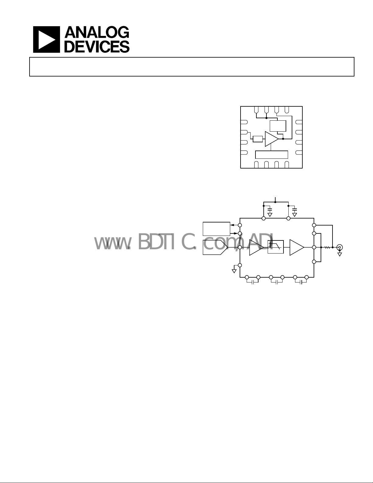
SYSTEM
CONTRO LLER
VIDEO
DAC/
ENCODER
with Load Detection
PIN CONFIGURATION
FB1
FB2
OUT
16
15
+V
1
S
2
IN
G = 2
DIS
LDO
LPF
3
4
CHARGE PUMP
5
6
CAP3
CAP4
Figure 1.
110
4
3
2
7
+V
LDO
DIS
IN
GND
CAP4 CAP3
56891112
S
ADA4431-1
x1 x2
CAP2 CAP1
0.1µF
Figure 2. Typical Application Circuit
SAG
14
13
LOAD
DETECT
7
8
GND
CAP2
+
S
0.1µF 0.1µF
+V
S
LPF
SUBS GND
0.1µF
ADA4431-1
12
GND
SUBS
11
10
+V
S
CAP1
9
06734-001
16
FB1
15
FB2
OUT
SAG
1.0µF
VIDEO
OUT
75Ω
14
13
6734-002
GENERAL DESCRIPTION
The ADA4431-1 is a fully integrated video reconstruction filter
that combines excellent video specifications with low power
consumption, making it ideal for portable video filtering
applications. The ADA4431-1 is able to detect whether a video
load is present at the output, powering down the device when
the load is disconnected.
The ADA4431-1 operates on single supplies as low as 2.5 V
w
hile providing the dynamic range required by the most
demanding video systems. The on-board charge pump
provides a virtual negative supply, allowing the video signal to
be dc-coupled and the black level to be set to ground, while the
sync passes cleanly at 300 mV below ground.
Rev. 0
Information furnished by Analog Devices is believed to be accurate and reliable. However, no
responsibility is assumed by Anal og Devices for its use, nor for any infringements of patents or ot her
rights of third parties that may result from its use. Specifications subject to change without notice. No
license is granted by implication or otherwise under any patent or patent rights of Analog Devices.
Trademarks and registered trademarks are the property of their respective owners.
When operating with the charge pump off, the ADA4431-1
rovides a dc offset to keep the sync tip approximately 100 mV
p
above ground. In addition, the part features SAG correction,
which permits the use of smaller capacitors in applications with
ac-coupled outputs.
The ADA4431-1 is packaged in a low profile 16-lead LFCSP and
perates in the industrial temperature range of −40°C to +85°C.
o
One Technology Way, P.O. Box 9106, Norwood, MA 02062-9106, U.S.A.
Tel: 781.329.4700 www.analog.com
Fax: 781.461.3113 ©2007 Analog Devices, Inc. All rights reserved.
Page 2

ADA4431-1
www.BDTIC.com/ADI
TABLE OF CONTENTS
Features .............................................................................................. 1
Applications....................................................................................... 1
Pin Configuration............................................................................. 1
General Description......................................................................... 1
Revision History ............................................................................... 2
Specifications..................................................................................... 3
Absolute Maximum Ratings............................................................ 5
Thermal Resistance ...................................................................... 5
Maximum Power Dissipation ..................................................... 5
ESD Caution.................................................................................. 5
REVISION HISTORY
8/07—Revision 0: Initial Version
Pin Configuration and Function Descriptions..............................6
Typical Perf or m an c e Charac t e r istics ..............................................7
Theory of Operation .........................................................................9
Overview ........................................................................................9
Charge Pump Operation..............................................................9
Load Detect....................................................................................9
Evaluation Board ............................................................................ 10
Outline Dimensions ....................................................................... 12
Ordering Guide .......................................................................... 12
Rev. 0 | Page 2 of 12
Page 3

ADA4431-1
www.BDTIC.com/ADI
SPECIFICATIONS
VS = 3.0 V (@ TA = 25°C, VIN = 1 V p-p, RL = 150 Ω, DIS = 3.0 V, charge pump on), unless otherwise noted.
Table 1.
Parameter Test Conditions/Comments Min Typ Max Unit
ELECTRICAL SPECIFICATIONS
Quiescent Supply Current
Normal Mode Video load present 4.7 7.2 mA
Load Searching Mode No video load 0.1 mA
Disabled Mode DIS = 0 V 24 μA
Disable Pin Current DIS = 3.0 V (enabled and charge pump on) 3 6 μA
DIS = 0 V (disabled) −17 −30 μA
Supply Voltage Range 2.5 3.6 V
Input Voltage Limited by output range 1.3 V
Input Resistance 10 MΩ
Input Capacitance 1 pF
Output Voltage Range −0.8 to +2.8 V
Output Offset Voltage −650 −600 −560 mV
Power Supply Rejection f = 100 kHz, output referred 36 42 dB
Pass-Band Gain 5.7 6.0 6.2 dB
Input-to-Output Isolation—Disabled f = 1 MHz, DIS = 0 V 89 dB
FILTER CHARACTERISTICS
−3 dB Bandwidth 7.1 7.9 9.1 MHz
1 dB Flatness 6 MHz
Out-of-Band Rejection f = 27 MHz 25 27 dB
Differential Gain Modulated 10 step ramp, sync tip at 0 V 0.7 %
Differential Phase Modulated 10 step ramp, sync tip at 0 V 0.3 Degrees
Linear Output Current 40 mA
Group Delay Variation f = 100 kHz to 5 MHz 30 ns
Rev. 0 | Page 3 of 12
Page 4
ADA4431-1
www.BDTIC.com/ADI
VS = 3.0 V (@ TA = 25°C, VIN = 1 V p-p, RL = 150 Ω, DIS = floating, charge pump off), unless otherwise noted.
Table 2.
Parameter Test Conditions/Comments Min Typ Max Unit
ELECTRICAL SPECIFICATIONS
Quiescent Supply Current
Normal Mode Video load present 1.6 2.2 mA
Load Searching Mode No video load 0.1 mA
Disabled Mode DIS = 0 V 24 μA
Disable Pin Current DIS = 0 V −17 −30 μA
Supply Voltage Range 2.5 3.6 V
Input Voltage Limited by output range 1.3 V
Input Resistance 10 MΩ
Input Capacitance 1 pF
Output Voltage Range 0 to 2.8 V
Output Offset Voltage 0.1 0.2 V
Power Supply Rejection f = 100 kHz, output referred 38 48 dB
Pass-Band Gain 5.8 6.0 6.2 dB
Input-to-Output Isolation—Disabled f = 1 MHz, DIS = 0 V 89 dB
FILTER CHARACTERISTICS
−3 dB Bandwidth 6.7 7.5 8.4 MHz
1 dB Flatness 6 MHz
Out-of-Band Rejection f = 27 MHz 26 29 dB
Differential Gain Modulated 10 step ramp, sync tip at 0 V 0.4 %
Differential Phase Modulated 10 step ramp, sync tip at 0 V 0.3 Degrees
Linear Output Current 40 mA
Group Delay Variation f = 100 kHz to 5 MHz 30 ns
Rev. 0 | Page 4 of 12
Page 5

ADA4431-1
www.BDTIC.com/ADI
ABSOLUTE MAXIMUM RATINGS
Table 3.
Parameter Rating
Supply Voltage 4.0 V
Power Dissipation See Figure 3
Storage Temperature Range –65°C to +125°C
Operating Temperature Range –40°C to +85°C
Lead Temperature (Soldering 10 sec) 300°C
Junction Temperature 150°C
Stresses above those listed under Absolute Maximum Ratings
may cause permanent damage to the device. This is a stress
rating only; functional operation of the device at these or any
other conditions above those indicated in the operational
section of this specification is not implied. Exposure to absolute
maximum rating conditions for extended periods may affect
device reliability.
THERMAL RESISTANCE
θJA is specified for the device (including exposed pad) soldered
The power dissipated in the package (P
quiescent power dissipation and the power dissipated in the
package due to the load drive. The quiescent power is the voltage
between the supply pins (V
The power dissipated due to the load drive depends upon the
particular application. The power due to load drive is calculated
by multiplying the load current by the associated voltage drop
across the device. RMS voltages and currents must be used in
these calculations.
Airflow increases heat dissipation, effectively reducing θ
addition, more metal directly in contact with the package leads
and exposed pad from metal traces, through-holes, ground, and
power planes reduces the θ
Figure 3 shows the maximum safe power dissipation in the
ackage vs. the ambient temperature for the 16-lead LFCSP
p
package (43°C/W) on a JEDEC standard 4-layer board.
5.0
4.5
to a high thermal conductivity 2s2p circuit board, as described
in EIA/JESD 51-7. The exposed pad is not electrically connected to
the device. It is typically soldered to a pad on the PCB that is
4.0
3.5
thermally and electrically connected to an internal ground plane.
3.0
Table 4. Thermal Resistance
Package Type θ
16-lead LFCSP-UQ (CP-16-12) 43 °C/W
JA
Unit
MAXIMUM POWER DISSIPATION
The maximum safe power dissipation in the ADA4431-1
2.5
2.0
MAXIMUM POWER DISSIPATION (W)
1.5
1.0
–40 –30 –20 –10 0 10 20 30 40 50 60 70 80 90 100
package is limited by the associated rise in junction temperature
(T
) on the die. At approximately 150°C, which is the glass
J
transition temperature, the plastic changes its properties. Even
temporarily exceeding this temperature limit can change the
Figure 3. Maximum Power Dissipation vs. Temperature for a 4-Layer Board
ESD CAUTION
stresses that the package exerts on the die, permanently shifting
the parametric performance of the ADA4431-1. Exceeding a
junction temperature of 150°C for an extended period can result in
changes in the silicon devices potentially causing failure.
) times the quiescent current (IS).
S
.
JA
AMBIENT TEM PERATURE (°C)
) is the sum of the
D
JA
. In
06743-003
Rev. 0 | Page 5 of 12
Page 6

ADA4431-1
www.BDTIC.com/ADI
PIN CONFIGURATION AND FUNCTION DESCRIPTIONS
FB1
FB2
OUT
16
+V
1
S
ADA4431-1
2
IN
DIS
LDO
3
4
TOP VIEW
(Not to Scale)
5
CAP4
Figure 4. Pin Configuration
Table 5. Pin Function Descriptions
Pin No. Mnemonic Description
1 +V
S
Supply Voltage.
2 IN Video Input.
3 DIS Disable Pin. High = charge pump on, floating = charge pump off, low = disabled.
4 LDO Load Detect Output. High = video load present.
5 CAP4 Capacitor 2, Lead 2.
6 CAP3 Capacitor 2, Lead 1.
7 GND Ground.
8 CAP2 Capacitor 1, Lead 2.
9 CAP1 Capacitor 1, Lead 1.
10 +V
S
Supply Voltage.
11 SUBS Substrate Voltage Pin. Bypass to GND with 1.0 μF capacitor.
12 GND Ground.
13 SAG SAG Feedback Pin.
14 OUT Video Output.
15 FB2 Load Detect Feedback Pin 2. Connect to device side of series termination resistor.
16 FB1 Load Detect Feedback Pin 1. Connect to load side of series termination resistor.
SAG
14
15
13
12
GND
SUBS
11
10
+V
S
CAP1
9
6
7
8
GND
CAP3
CAP2
06743-004
Rev. 0 | Page 6 of 12
Page 7

ADA4431-1
–
www.BDTIC.com/ADI
TYPICAL PERFORMANCE CHARACTERISTICS
VS = 3.0 V (@ TA = 25°C, VIN = 1 V p-p, RL = 150 Ω, unless otherwise noted).
–10
–20
10
0
CHARGE PUMP ON
60
50
40
–30
–40
NORMALIZED GAIN (dB)
–50
–60
–70
0.1 1 10 100
CHARGE PUMP OFF
FREQUENCY (MHz)
Figure 5. Large Signal Frequency Response
1
CHARGE PUMP ON
0
–1
–2
CHARGE PUMP OFF
–3
NORMALIZED GAIN (dB)
–4
–5
0.1 1 10
FREQUENCY (MHz)
Figure 6. Frequency Response Flatness
60
DIS = 0V
–65
–70
–75
–80
–85
–90
NORMALIZED GAIN (dB)
–95
–100
–105
0.1 1 10 100
FREQUENCY (MHz )
Figure 7. Input-to-Output Isolation vs. Frequency
30
20
GROUP DELAY (ns)
10
0
0.1 1 10 100
06734-005
CHARGE PUMP OFF
CHARGE PUMP ON
FREQUENCY (MHz)
06734-008
Figure 8. Group Delay vs. Frequency
0
VIN = 100mV p-p
DIS = 3V
–5
–10
–15
–20
–25
PSRR (dB)
–30
–35
–40
–45
–50
06734-006
CHARGE PUMP ON
CHARGE PUMP OF F
0.1 1 10 100
FREQUENCY (MHz)
06734-009
Figure 9. PSRR vs. Frequency
10
0
–10
–20
–30
–40
NORMALIZED GAIN (dB)
–50
–60
0.1 1 10 100
06734-007
FREQUENCY (MHz)
+85°C
+25°C
0°C
–40°C
06734-010
Figure 10. Frequency Response for Various Temperatures
Rev. 0 | Page 7 of 12
Page 8

ADA4431-1
www.BDTIC.com/ADI
1
0
+85°C
–1
+25°C
0°C
–40°C
–2
–3
–4
NORMALIZED GAIN (dB)
–5
–6
–7
0.1 1 10
FREQUENCY (MHz )
Figure 11. Flatness Response for Various Temperatures
6
5
4
3
2
06734-011
DISABLE (DIS ) PIN
1
T
CH2 200mV M100ns A CH1 316mV
Figure 14. Transient Response
T
06734-015
2
SUPPLY CURRENT (mA)
1
0
03.02.52.01.51.00.5
DISABLE (DIS ) PIN VOL TAGE (V)
Figure 12. Supply Current vs. Disable (DIS) Pin Voltage
7
6
5
4
3
2
SUPPLY CURRENT (mA)
1
0
–40 –30 –20 –10 0 10 20 30 40 50 60 70 80 90
ACTIVE
DISABLED
TEMPERATURE (°C)
Figure 13. Supply Current vs. Temperature
2
06734-012
CH1 2.00V CH2 500mV M10.0ms A CH1 1.72V
OUTPUT
06734-016
Figure 15. Output Enable
70
60
50
40
30
20
DISABLED SUPPL Y CURRENT (µA)
10
0
06734-014
1
2
CH1 2.00V CH2 500mV M40.0ns A CH1 1.72V
T
DISABLE (DIS) PIN
OUTPUT
06734-017
Figure 16. Output Disable
Rev. 0 | Page 8 of 12
Page 9

ADA4431-1
www.BDTIC.com/ADI
THEORY OF OPERATION
OVERVIEW
The ADA4431-1 is designed for exceptional performance as
both a filter and a low power driver for portable video applications.
This performance is achieved by providing third-order filtering
without trading off power consumption or device size. While
consuming only 4.7 mA quiescent supply current, the ADA4431-1
provides video output on a single-supply as low as 2.5 V.
The ADA4431-1 also features a load detect circuit, which senses
urrent through the external 75 Ω back-termination resistor.
c
When either no video load or a short circuit is detected, the
ADA4431-1 enters a low power state. In this state, it draws
0.1 mA, continues to monitor the load current, and powers up
automatically when a video load is connected. Optionally, the
ADA4431-1 can be powered down via the disable pin (DIS).
Another external pin (LDO) outputs the load detection state
(for example, to an external system controller). This pin is high
(+V
) when a video load is present, and low (0 V) in the absence
S
of a video load or when the output is short-circuited.
The ADA4431-1 is intended for use in applications that have
b
oth ac- and dc-coupled inputs and outputs. The rail-to-rail
buffer on the ADA4431-1 output is able to drive 2 V p-p video
signals into two doubly terminated video loads (150 Ω each) on
a single 2.5 V supply. The ADA4431-1 has a gain of 2 when the
SAG correction pin is tied directly to the output, which makes
up for the 6 dB termination loss (see
W
hen the SAG feature is used, the ADA4431-1 has a low
frequency gain of 2.5 (≈8 dB) and a high frequency gain of 2
(see Figure 17, Output Option 2). Signal offsets and supply levels
m
ust be considered when using the SAG correction feature to
ensure that there are no headroom issues.
The input range of the ADA4431-1 includes ground, while the
utput range is limited by the saturation of the output devices.
o
Saturation occurs several tens of mV from the positive and
negative supply rails.
Figure 17, Output Option 1).
The high input impedance and low input capacitance of the
A4431-1 offer advantages in a number of low power
AD
applications. In reconstruction filter applications, the DAC can
be placed in its lowest power mode, allowing the use of a largevalued load resistor. Using a large-valued load resistor does not
interfere with the frequency response of the ADA4431-1.
CHARGE PUMP OPERATION
The on-board charge pump creates a virtual negative supply for
the output driver, which allows the output signal to be dc-coupled,
with its black level at 0 V and sync tip at −300 mV. The charge
pump is enabled whenever the disable pin (DIS) is held high.
If DIS is left floating, or placed in a high impedance state, the
ADA4431-1 is powered up, but the charge pump is disabled,
which is typically the case for ac-coupling of the output. When
DIS is driven to 0 V, the entire device is powered down.
Table 6. Disable (DIS) Pin Function Summary
DIS Pin Device State Charge Pump State
Low Disabled Disabled
High Enabled Enabled
High-Z Enabled Disabled
LOAD DETECT
The load detect feature provides additional system power
management to keep the power consumption of a portable
device to the absolute minimum. The ADA4431-1 monitors the
output load for three conditions: a normal load, a shorted load,
and an open load. Each of these conditions occurs for a video
load, an audio load, and no load, respectively. Only in the video
load condition will the ADA4431-1 power up from 0.1 mA to
4.7 mA. A single I/O pin, LDO, notifies the system by either
being high for a video load or low for a short and open load.
With this information, it is intended that the system controller
power down any power intensive video processing blocks to
realize substantial power savings. The ADA4431-1 operates
autonomously, requiring no inputs to monitor the condition of
the output load.
Rev. 0 | Page 9 of 12
Page 10

ADA4431-1
www.BDTIC.com/ADI
EVALUATION BOARD
The ADA4431-1 evaluation board allows designers to assess
the performance of the part in their particular application. The
board includes input and output SMA coaxial connectors and
75 Ω-controlled impedance signal traces. Power (2.5 V to 3.6 V)
is applied to the red V+ loop connector, and ground is connected
to the black GND loop connector.
The output signal can be configured for dc coupling or ac
c
oupling. When ac-coupled, two options are available: the
standard single capacitor configuration (minimum of 220 μF)
and the SAG-corrected configuration, using two smaller
capacitors (47 μF and 22 μF).
Jumper Block J2 allows the load detect feature to be evaluated
thout connecting an external video load. Connecting a
wi
jumper from the center pin to the 75 position applies a 75 Ω
load to the output and causes the LDO pin to go high.
OUTPUT OPTION 1
14
IN
DIS
C8
10µF
C5
0Ω
C4
0Ω
AC-COUPLED
OUTPUT
13
R2
75Ω
R3
DNI
J4
GND
DIS
V+
+
V+
C6
220µF
+
0.1µF
V+
16
2
+V
IN
DIS
LDO
15
S
FB1
ADA4431-1
CAP4
5
C1
0.1µF
LDO
C9
DNI
1
3
4
R4
LDOUT
R1
0Ω
Figure 17. Evaluation Board Schematic
FB2
AP3
C
6
Connecting the center pin to the GND position short circuits
the output, causing the ADA4431-1 to power down, and the
LDO pin to go low. If an external video load is connected to
the OUT connector, the jumper should be removed. With the
jumper removed, disconnecting the external load also causes
the ADA4431-1 to power down.
Jumper Block J4 exercises the disable pin (DIS). When a jumper
nnected from the center pin to V+, the charge pump is
is co
enabled. Connecting the center pin to GND forces the ADA4431-1
into low power mode. With the jumper removed, the ADA4431-1
is enabled but the charge pump is disabled.
A schematic of the ADA4431-1 evaluation board, with output
oupling options, is shown in Figure 17. Figure 18 and Figure 19
c
sh
ow the front and back layout of the evaluation board.
R6
75Ω
J2
C5
0Ω
14
OUT
GND
7
C6
0Ω
C4
0Ω
DC-COUPLED
OUTPUT
13
GND
12
SAG
11
SUBS
+V
S
10
CAP1
9
CAP2
8
C2
0.1µF
75Ω
75Ω
R5
GND
LD2
C3
1.0µF
C7
0.1µF
SUBS
V+
OUTPUT OPTION 2
47µF
14
AC-COUPLED OUT PUT
WITH SAG CORRECTION
OUT
GND
C5
C6
0Ω
+
+
C4
22µF
13
06734-018
Rev. 0 | Page 10 of 12
Page 11

ADA4431-1
www.BDTIC.com/ADI
06743-019
Figure 18. Evaluation Board—Front
Figure 19. Evaluation Board—Back
06743-020
Rev. 0 | Page 11 of 12
Page 12

ADA4431-1
www.BDTIC.com/ADI
OUTLINE DIMENSIONS
INDEX
AREA
0.60
0.55
0.51
SEATING
PLANE
3.00
BSC SQ
13
12
0.50
BSC
TOP VIEW BOTTOM VIEW
0.05 MAX
0.02 NOM
0.30
0.25
0.18
0.08 REF
9
8
EXPOSED
PAD
16
5
N
I
1
P
N
I
1
4
1.80
1.70 SQ
1.55
0.40 MAX
0.30 NOM
R
A
O
T
D
C
I
COMPLIANTTOJEDEC STANDARDS MO-248-UEED.
053106-B
Figure 20. 16-Lead Lead Frame Chip Scale Package [LFCSP_UQ]
3 mm
× 3 mm Body, Ultra Thin Quad
(CP-16-12)
Dimensions shown in millimeters
ORDERING GUIDE
Model Temperature Range Package Description Package Option Branding Ordering Quantity
ADA4431-1YCPZ-R2
ADA4431-1YCPZ-R7
ADA4431-1YCPZ-RL
1
Z = RoHS Compliant Part.
1
−40°C to +85°C 16-Lead LFCSP_UQ CP-16-12 H12 250
1
−40°C to +85°C 16-Lead LFCSP_UQ CP-16-12 H12 3,000
1
−40°C to +85°C 16-Lead LFCSP_UQ CP-16-12 H12 10,000
©2007 Analog Devices, Inc. All rights reserved. Trademarks and
registered trademarks are the property of their respective owners.
D06734-0-8/07(0)
T
Rev. 0 | Page 12 of 12
TTT
 Loading...