

Ultralow Power Video Filter
www.BDTIC.com/ADI
FEATURES
6th-order performance, low-pass video filter
1 dB flatness out to 8 MHz
50 dB rejection at 27 MHz
Ultralow power-down current: 0.1 μA typ
Low quiescent current: 1.85 mA typ
Excellent video specification
Differential gain: 0.25%
Differential phase: 0.10°
SAG correction
Allows use of small capacitors in ac-coupled outputs
Low supply voltage: 2.5 V to 6 V
Rail-to-rail output
High input-to-output isolation in disabled state
92 dB @ 1 MHz
Low input bias current: 0.5 μA
Small packaging: SC70
Wide operating temperature range: −40°C to +125°C
APPLICATIONS
Portable media players
Portable gaming consoles
Cell phones
Digital still cameras
Portable DVD players
Portable video cameras
with Power-Down
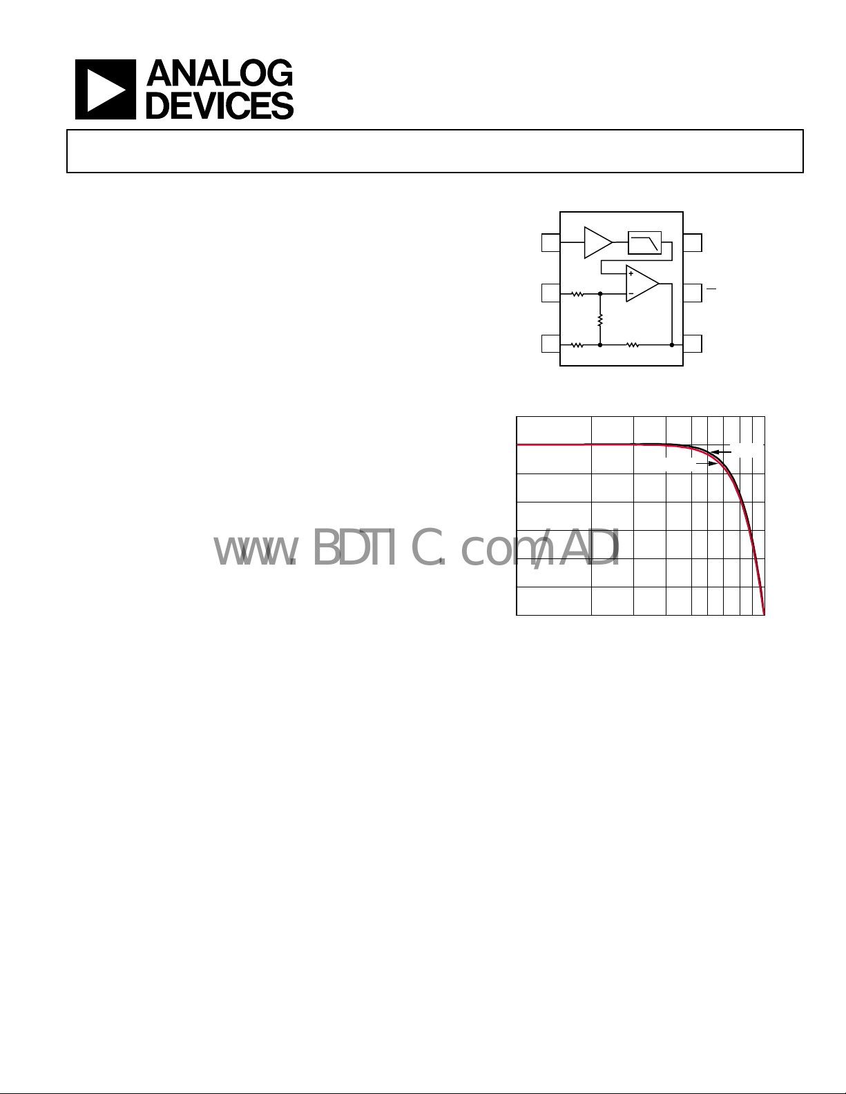
ADA4430-1
PIN CONFIGURATION
ADA4430-1
V
IN
GND
SAG
6.5
6.0
5.5
5.0
4.5
GAIN (dB)
4.0
3.5
3.0
11
Figure 2. Frequency Response Fla
x1
1
2*R
2
R
2*R
3
2*R
Figure 1.
VS = 5V
FREQUENCY (MHz)
tness at Various Power Supplies
+
V
6
S
5
PD
4
V
OUT
05885-001
VS = 3V
05885-006
0
GENERAL DESCRIPTION
The ADA4430-1 is a fully integrated video reconstruction filter
that combines excellent video specifications with low power
consumption and an ultralow power disable, making it ideal
for portable video filtering applications. With 1 dB frequency
flatness out to 8 MHz and 50 dB rejection at 27 MHz, the
ADA4430-1 is ideal in SD video applications, including
NTSC and PAL.
The ADA4430-1 operates on single supplies as low as 2.5 V and
h as 6 V while providing the dynamic range required by
as hig
the most demanding video systems.
Rev. A
Information furnished by Analog Devices is believed to be accurate and reliable. However, no
responsibility is assumed by Anal og Devices for its use, nor for any infringements of patents or ot her
rights of third parties that may result from its use. Specifications subject to change without notice. No
license is granted by implication or otherwise under any patent or patent rights of Analog Devices.
Trademarks and registered trademarks are the property of their respective owners.
The ADA4430-1 also provides an on-chip dc offset to avoid
c
lipping of the sync tips at the filter output, as well as SAG
correction that permits smaller capacitor values to be used in
applications with ac-coupled outputs.
The ADA4430-1 is available in a 6-lead SC70 package and is
r
ated to work in the extended automotive temperature range of
−40°C to +125°C.
One Technology Way, P.O. Box 9106, Norwood, MA 02062-9106, U.S.A.
Tel: 781.329.4700 www.analog.com
Fax: 781.461.3113 ©2006 Analog Devices, Inc. All rights reserved.

ADA4430-1
www.BDTIC.com/ADI
TABLE OF CONTENTS
Features .............................................................................................. 1
Theory of Operation ...................................................................... 11
Applications....................................................................................... 1
Pin Configuration............................................................................. 1
General Description......................................................................... 1
Revision History ............................................................................... 2
Specifications..................................................................................... 3
Absolute Maximum Ratings............................................................ 4
Thermal Resistance ...................................................................... 4
ESD Caution.................................................................................. 4
Pin Configuration and Function Descriptions............................. 5
Typical Performance Characteristics ............................................. 6
Test Cir c ui t s .....................................................................................10
REVISION HISTORY
6/06—Rev. 0 to Rev. A
Changes to Figure 1.......................................................................... 1
Changes to Figure 4.......................................................................... 5
Overview ..................................................................................... 11
Power Savings Using the ADA4430-1 ..................................... 11
Applications..................................................................................... 12
Examples Illustrating Output Coupling.................................. 12
Usable Input Voltage Range ...................................................... 13
SAG Correction Frequency Response..................................... 13
Reconstruction Filter Applications.......................................... 14
Printed Circuit Board Layout ................................................... 15
Outline Dimensions ....................................................................... 16
Ordering Guide .......................................................................... 16
3/06—Revision 0: Initial Version
Rev. A | Page 2 of 16

ADA4430-1
www.BDTIC.com/ADI
SPECIFICATIONS
VS = 3 V @ TA = 25°C, VIN = 1 V p-p, RL = 150 Ω, unless otherwise noted.
Table 1.
Parameter Test Conditions/Comments Min Typ Max Unit
ELECTRICAL SPECIFICATIONS
Quiescent Supply Current 1.85 2.3 mA
Quiescent Supply Current—Disabled 0.1 5 μA
Supply Voltage 2.5 6 V
Input Voltage Range—Low/High Limited by output range; see the Applications section 0/1.38 V
Input Resistance 10 MΩ
Input Capacitance 1 pF
Input Bias Current 0.5 μA
Output Voltage Range—Low/High 0.10/2.85 V
Output Offset Voltage 95 140 mV
PSRR Input referred 50 60 dB
Pass-Band Gain 5.85 6 dB
Input-to-Output Isolation—Disabled f = 1 MHz 92 dB
FILTER CHARACTERISTICS
−3 dB Bandwidth 7 9.7 MHz
1 dB Flatness 5.5 8.0 MHz
Out-of-Band Rejection f = 27 MHz 40 50 dB
Differential Gain Modulated 10 step ramp, sync tip at 0 V 0.25 %
Differential Phase Modulated 10 step ramp, sync tip at 0 V 0.10 Degrees
Linear Output Current 40 mA
Group Delay Variation f = 100 kHz to 5 MHz 7 ns
Signal-to-Noise Ratio 100% white signal, f = 100 kHz to 5 MHz 76 dB
VS = 5 V @ TA = 25°C, VIN = 1 V p-p, RL = 150 Ω, unless otherwise noted.
Table 2.
Parameter Test Conditions/Comments Min Typ Max Unit
ELECTRICAL SPECIFICATIONS
Quiescent Supply Current 2.0 2.4 mA
Quiescent Supply Current—Disabled 0.2 10 μA
Supply Voltage 2.5 6 V
Input Voltage Range—Low/High Limited by output range; See the Applications section 0/2.35 V
Input Resistance 10 MΩ
Input Capacitance 1 pF
Input Bias Current 0.5 μA
Output Voltage Range—Low/High 0.10/4.80 V
Output Offset Voltage 100 145 mV
PSRR Input referred 50 61 dB
Pass-Band Gain 5.85 6 dB
Input-to-Output Isolation—Disabled f = 1 MHz 92 dB
FILTER CHARACTERISTICS
−3 dB Bandwidth 7.2 9.5 MHz
1 dB Flatness 5.5 7.9 MHz
Out-of-Band Rejection f = 27 MHz 40 50 dB
Differential Gain Modulated 10 step ramp, sync tip at 0 V 0.25 %
Differential Phase Modulated 10 step ramp, sync tip at 0 V 0.15 Degrees
Linear Output Current 40 mA
Group Delay Variation f = 100 kHz to 5 MHz 7.1 ns
Signal-to-Noise Ratio 100% white signal, f = 100 kHz to 5 MHz 76 dB
Rev. A | Page 3 of 16

ADA4430-1
www.BDTIC.com/ADI
ABSOLUTE MAXIMUM RATINGS
Table 3.
Parameter Rating
Supply Voltage 6 V
Power Dissipation See Figure 3
Storage Temperature Range –65°C to +125°C
Operating Temperature Range –40°C to +125°C
Lead Temperature (Soldering 10 sec) 300°C
Junction Temperature 150°C
Stresses above those listed under Absolute Maximum Ratings
may cause permanent damage to the device. This is a stress
rating only; functional operation of the device at these or any
other conditions above those indicated in the operational
section of this specification is not implied. Exposure to absolute
maximum rating conditions for extended periods may affect
device reliability.
THERMAL RESISTANCE
θJA is specified for the worst-case conditions, that is, θJA is
specified for a device soldered in the circuit board.
Table 4. Thermal Resistance
Package Type θ
6-Lead SC70 430 °C/W
JA
Maximum Power Dissipation
The maximum safe power dissipation in the ADA4430-1
package is limited by the associated rise in junction temperature
(T
) on the die. At approximately 150°C, which is the glass
J
transition temperature, the plastic changes its properties. Even
temporarily exceeding this temperature limit can change the
stresses that the package exerts on the die, permanently shifting
the parametric performance of the ADA4430-1. Exceeding a
junction temperature of 150°C for an extended period can
Unit
The power dissipated in the package (P
quiescent power dissipation and the power dissipated in the
package due to the load drive. The quiescent power is the
voltage between the supply pins (V
current (I
). The power dissipated due to the load drive depends
S
upon the particular application. The power due to load drive is
calculated by multiplying the load current by the associated
voltage drop across the device. RMS voltages and currents must
be used in these calculations.
Airflow increases heat dissipation, effectively reducing θ
addition, more metal directly in contact with the package leads
from metal traces, through-holes, ground, and power planes
reduces the θ
.
JA
Figure 3 shows the maximum safe power dissipation in the
p
ackage vs. the ambient temperature for the 6-lead SC70
(430°C/W) on a JEDEC standard 4-layer board.
0.50
0.45
0.40
0.35
0.30
0.25
0.20
0.15
0.10
MAXIMUM POWER DISSIPATION (W)
0.05
0
–40 120100806040020–20
Figure 3. Maximum Power Dissipation vs. Temperature for a 4-Layer Board
result in changes in the silicon devices potentially causing
failure.
AMBIENT TEMP ERATURE (°C)
) is the sum of the
D
) times the quiescent
S
JA
. In
05885-002
ESD CAUTION
ESD (electrostatic discharge) sensitive device. Electrostatic charges as high as 4000 V readily accumulate on
the human body and test equipment and can discharge without detection. Although this product features
proprietary ESD protection circuitry, permanent damage may occur on devices subjected to high energy
electrostatic discharges. Therefore, proper ESD precautions are recommended to avoid performance
degradation or loss of functionality.
Rev. A | Page 4 of 16
ADA4430-1
www.BDTIC.com/ADI
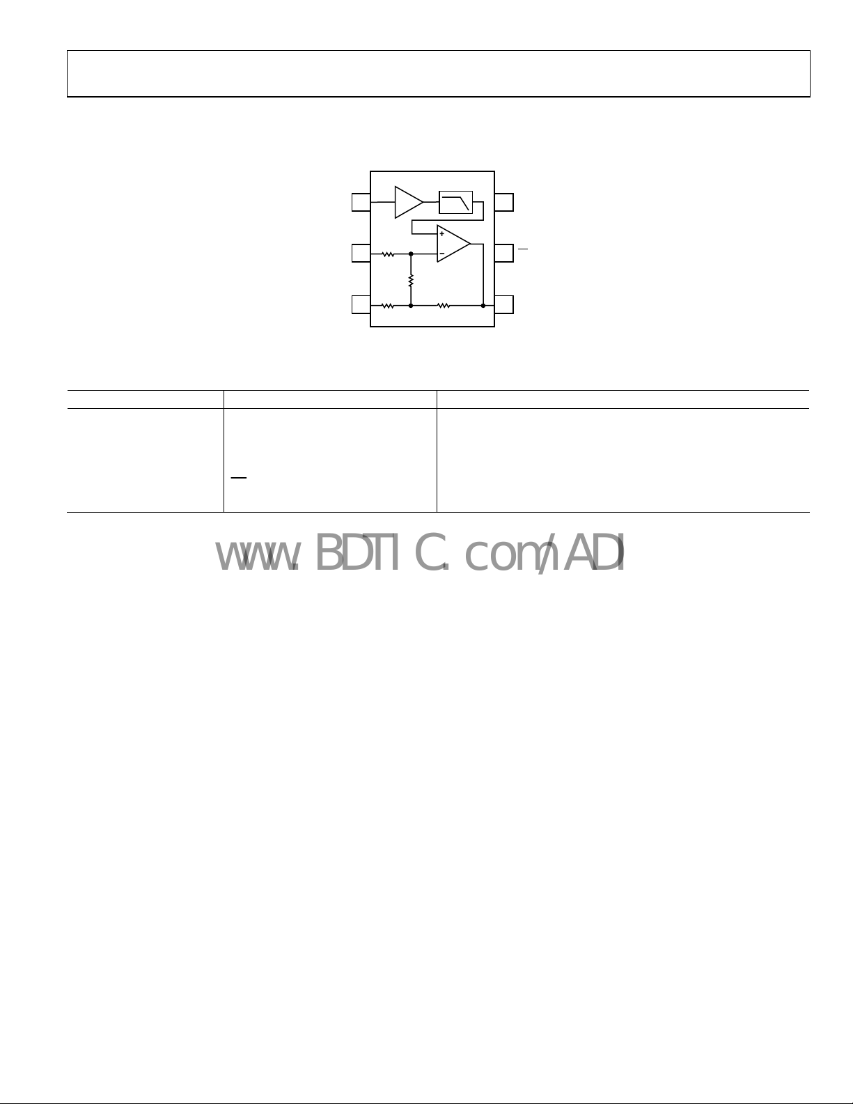
PIN CONFIGURATION AND FUNCTION DESCRIPTIONS
ADA4430-1
V
IN
x1
1
+
V
6
S
GND
SAG
2*R
2
R
2*R
3
Figure 4. 6-Lead SC70, Top View
2*R
5
PD
4
V
OUT
05885-041
Table 5. Pin Function Descriptions
Pin Number Mnemonic Description
1 V
IN
Input Voltage.
2 GND Ground.
3 SAG Feedback Connection.
4 V
5
6 V
OUT
PD
S+
Output Voltage.
Power Down.
Positive Power Supply.
Rev. A | Page 5 of 16

ADA4430-1
www.BDTIC.com/ADI
TYPICAL PERFORMANCE CHARACTERISTICS
VS = +3 V, RL, = 150 Ω, V
9
6
3
0
–3
–6
–9
–12
–15
–18
–21
–24
GAIN (dB)
–27
–30
–33
–36
–39
–42
–45
–48
–3
–6
–9
–12
–15
–18
–21
–24
GAIN (dB)
–27
–30
–33
–36
–39
–42
–45
–48
–3
–6
–9
–12
–15
–18
–21
–24
GAIN (dB)
–27
–30
–33
–36
–39
–42
–45
–48
11
Figure 5. Frequency Response at Various Power Supplies
9
6
3
0
11
Figure 6. Frequency Response at Various Loads
9
6
3
0
11
Figure 7. Frequency Response at Various Temperatures
= 2.0 V p-p, PD = high, V
OUT
VS = 3V
V
= 5V
S
FREQUENCY (MHz)
RL = 75Ω
FREQUENCY (MHz)
RL = 150Ω
FREQUENCY (MHz)
connected directly to SAG, TA = 25°C, unless otherwise noted.
OUT
6.5
6.0
5.5
5.0
4.5
GAIN (dB)
4.0
3.5
05885-003
0010
3.0
110
Figure 8. Frequency Response Fla
FREQUENCY (MHz)
tness at Various Power Supplies
6.5
6.0
5.5
5.0
4.5
GAIN (dB)
4.0
3.5
05885-004
0010
3.0
110
FREQUENCY (MHz)
Figure 9. Frequency Response Flatness at Various Loads
+125°C
+25°C
–40°C
05885-005
0010
6.5
6.0
5.5
5.0
4.5
GAIN (dB)
4.0
3.5
3.0
110
FREQUENCY (MHz)
Figure 10. Frequency Response Flatness at Various Temperatures
VS = 5V
VS = 3V
05885-006
RL = 75Ω
RL = 150Ω
05885-007
+125°C
+25°C
–40°C
05885-008
Rev. A | Page 6 of 16

ADA4430-1
–
–
www.BDTIC.com/ADI
9
6
3
0
–3
–6
–9
–12
–15
–18
–21
–24
GAIN (dB)
–27
–30
–33
–36
–39
–42
–45
–48
11
2.0V p-p
0.2V p-p
10
FREQUENCY (MHz)
Figure 11. Frequency Response at Various Output Amplitudes
50
NOISE SPECTRUM (NTSC)
–55
INPUT REFERRED
–60
BANDWIDTH 100kHz TO 5.0MHz
–65
AMPLI TUDE (0d B = 714mV p-p)
–70
NOISE L EVEL = –76.8dB rms
–75
–80
–85
–90
–95
–100
(dB)
–105
–110
–115
–120
–125
–130
–135
–140
–145
–150
1065432
FREQUENCY (MHz)
Figure 12. Input-Referred Noise Spectral Density
40
VIN = 1V p-p
V
= 0V
DIS
–50
OUTPUT REFERRED
–60
–70
–80
–90
ISOLATION (dB)
–100
–110
–120
–130
0.01 1001010.1
Figure 13. Input-to-Output Isolatio
FREQUENCY (MHz)
n—Disabled vs. Frequency
05885-009
00
05885-010
05885-011
65
60
55
50
45
GROUP DELAY (ns)
40
35
30
110010
VS = 5V
FREQUENCY (MHz)
VS = 3V
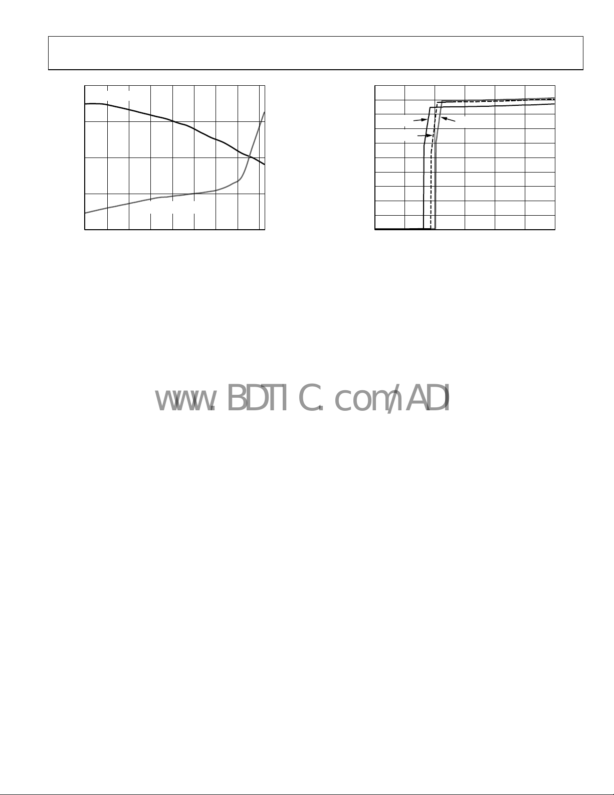
Figure 14. Group Delay at Various Power Supplies
0
INPUT REFERRED
–5
–10
–15
–20
–25
–30
–35
PSRR (dB)
–40
–45
–50
–55
–60
–65
0.001 0.01 1001010.1
FREQUENCY (MHz)
3V
Figure 15. PSRR vs. Frequency at Various Power Supplies
10000
V
DISABLE
1000
IMPEDANCE (Ω)
100
10
0.1 1 10 100 500
Figure 16. Disabled Output Imped
FREQUENCY (MHz)
ance vs. Frequency
05885-012
5V
05885-013
=0V
05885-030
Rev. A | Page 7 of 16

ADA4430-1
–
www.BDTIC.com/ADI
3.0
2.5
2.0
1.5
1.0
OUTPUT VOLTAGE (V)
0.5
100ns/DIV
0
05885-015
3.00
2.75
2.50
2.25
2.00
1.75
1.50
1.25
1.00
OUTPUT VOLTAGE (V)
0.75
0.50
0.25
0
INPUT × 2
OUTPUT
ERROR
50ns/DIV
3.0
2.5
2.0
1.5
1.0
0.5
0
–0.5
–1.0
–1.5
–2.0
–2.5
–3.0
ERROR (%)
05885-018
Figure 17. Transient Response
3.5
3.0
2.5
2.0
1.5
1.0
OUTPUT VOLTAGE (V)
0.5
0
–0.5
DISABLEDISABLE
OUTPUT
1µs/DIV
05885-016
3.5
3.0
2.5
2.0
1.5
1.0
OUTPUT VOLTAGE (V)
0.5
0
–0.5
Figure 18. Disable Assert Time
4.0
3.5
3.0
2.5
2.0
1.5
1.0
OUTPUT (V)
0.5
0
–0.5
–1.0
OUTPUT
2× INPUT
200ns/DIV
05885-033
Figure 19. Overdrive Recovery
0.10
–0.11
(V)
–0.12
OUT
–0.13
AND V
S
–0.14
–0.15
–0.16
–0.17
–0.18
–0.19
DIFFERENCE BETWEEN V
–0.20
–40 –25 –10 5 20 35 50 65 80 95 110 125
Figure 22. Output Swing Li
Figure 20. Settling Time
DISABLE
OUTPUT
500ns/DIV
Figure 21. Disable Deassert Time
TEMPERATURE (°C)
mits vs. Temperature
05885-019
05885-031
Rev. A | Page 8 of 16
ADA4430-1
www.BDTIC.com/ADI
1.85
ENABLED (V
1.80
1.75
1.70
POWER SUPPLY CURRENT–ENABL ED (mA)
1.65
= 3V)
DIS
DISABLED (V
TEMPERATURE ( °C)
DIS
= 0V)
Figure 23. Power Supply Current vs. Temperature
400
300
200
100
POWER SUPPLY CURRENT–DIS ABLED (nA)
05885-021
0
120100806040200–20–40
2.0
1.8
1.6
+125°C
1.4
1.2
1.0
0.8
0.6
0.4
POWER SUPPL Y CURRENT (mA)
0.2
+25°C
0
–40°C
DISABLE VOLTAGE (V)
05885-022
3.02.52.01.51.00.50
Figure 24. Power Supply Current vs. Disable Voltage at Various Temperatures
Rev. A | Page 9 of 16

ADA4430-1
V
R
V
www.BDTIC.com/ADI
TEST CIRCUITS
S+
0.1µF
50Ω
1
2
3
ADA4430-1
V
IN
×1
GND
SAG
2.6kΩ
2.6kΩ
0.5V
TEST GENERATOR
50Ω
Figure 25. Test Circuit Used for Frequency Sweeps and T
ADA4430-1
TEST GE NERATO
75Ω
220µF
1.0V
150Ω
150Ω
1
V
IN
×1
GND
2
3
SAG
2.6kΩ
2.6kΩ
PD
1.3kΩ
PD
1.3kΩ
5
5
6
V
V
2.6kΩ
S+
6
V
V
2.6kΩ
S+
OUT
S+
OUT
= 150Ω
R
L
118Ω
4
ime-Domain Tests
0.1µF
R
= 150Ω
L
75Ω
4
TEST RECEIVER
50Ω86.6Ω
TEST RECEIVER
75Ω
05885-038
Figure 26. Test Circuit Used for Differential Ga
in, Differential Phase, and Noise Tests
05885-039
Rev. A | Page 10 of 16

ADA4430-1
V
V
www.BDTIC.com/ADI
THEORY OF OPERATION
OVERVIEW
The ADA4430-1 is designed for exceptional performance as
both a filter and a low power driver for portable video
applications. This performance is achieved by providing high
order filtering without trading off power consumption or device
size. While consuming only 1.85 mA quiescent supply current,
the ADA4430-1 provides video output on a single-supply as low
as 2.5 V. Such low power consumption and low supply operation
would normally indicate a single op amp with a 2- or 3-pole
roll-off; however, the ADA4430-1 achieves a sixth-order roll-off
in addition to a 10 MΩ input impedance for easy clamping and
lower DAC output power requirements. When not in use, the
ADA44330-1 can be shutdown to draw less than 1 µA of supply
current using the power-down pin, (
ADA4430-1 is unique in that it is a high order filter that fits into
an SC70 package.
The ADA4430-1 provides a minimum 1 dB bandwidth of
z and a minimum stop-band rejection of 42 dB at
5.5 MH
27 MHz. Phase response is not sacrificed in spite of the
exceptional filtering performance of the ADA4430-1, as
exhibited by its group delay, which varies by only 7 ns from
100 kHz to 5 MHz.
The ADA4430-1 is intended for use in applications that have
b
oth ac- and dc-coupled inputs and outputs. The rail-to-rail
buffer on the ADA4430-1 output is able to drive 2 V p-p video
signals into two doubly-terminated video loads (150 Ω each) on
a single 2.5 V supply. The ADA4430-1 has a gain of 2 when the
SAG correction pin is tied directly to the output, which makes
up for the 6 dB termination loss. When the SAG feature is used
(see
Figure 29), the ADA4430-1 has a low frequency gain of
2.5 (≈ 8 dB) a
nd a high frequency gain of 2. Signal offsets and
supply levels must be considered when using the SAG correction
feature to ensure that there are no headroom issues.
PD
). Additionally, the
The internal buffer at the ADA4430-1 input isolates the source
r
esistance feeding the ADA4430-1 from the internal filter networks.
High input impedance is also advantageous when using video
clamping circuits.
The output buffer feedback network used to create a gain of 2 is
nnected internally to the GND pin and has a nominal impedance
co
of 5.2 k. The current required to drive this feedback network
causes the overall supply current to vary based on the output
level. The feedback impedance was chosen specifically to
minimize excess current consumption while maintaining
optimal frequency behavior.
POWER SAVINGS USING THE ADA4430-1
Using a series source termination and a shunt load termination
on a low supply voltage with the ADA4430-1 realizes significant
power savings compared with driving a video cable directly from
a DAC output.
irectly. Properly terminating the line results in the DAC driving
d
two 75 Ω loads and requires in excess of 30 mA to reach a fullscale level of 1.3 V.
iven using the ADA4430-1 and a series-shunt termination. This
dr
requires two times the output voltage to drive the equivalent of
150 Ω but only requires a little more than 15 mA to reach a fullscale output. When running on the same supply voltage as the
DAC, this results in nearly a factor of two reduction in power
compared with the circuit in
f
iltering provided by the ADA4430-1 lowers the requirements
on the DAC oversampling ratio, realizing further power savings.
On any given DAC, 8× and 16× oversampling ratios can require
twice the power consumption of a 4× oversampling ratio.
Figure 27 shows a video DAC driving a cable
Figure 28 shows the same video load being
Figure 27. The high level of
3
VIDEO
DAC/
ENCODER
75Ω
75Ω
The input range of the ADA4430-1 includes ground, while the
utput range is limited by the saturation of the output devices.
o
Saturation occurs several tens of mV from the positive and
negative supply rails. For accurate reproduction of groundreferenced input signals, an internal offset is used to shift the
output up by 95 mV.
The high input impedance and low input capacitance of the
AD
A4430-1 offer advantages in a number of low power
applications. In reconstruction filter applications, the DAC can
be placed in its lowest power mode, allowing the use of a largevalued load resistor. Using a large-valued load resistor does not
interfere with the frequency response of the ADA4430-1.
Rev. A | Page 11 of 16
Figure 27. DAC Driving Video Cable Directly
3
0.1µF
VIDEO
DAC/
ENCODER
Figure 28. DAC Driving Video Cable Using the ADA4430-1
ADA4430-1
R
L
FILTER
G = +2
75Ω
05885-034
75Ω
05885-035

ADA4430-1
V
V
V
T
V
www.BDTIC.com/ADI
APPLICATIONS
EXAMPLES ILLUSTRATING OUTPUT COUPLING
The ADA4430-1 is ideally suited for use as a reconstruction
filter that follows a video DAC or encoder. The application
circuits in Figure 29, Figure 30, and Figure 31 illustrate a
n
umber of ways the ADA4430-1 can be used with a singlesupply current-output DAC on its input and its output ac- and
dc-coupled.
SAG correction allows the use of two small, lower cost
ca
pacitors in place of one large capacitor in applications with
ac-coupled outputs. Circuits with ac-coupled outputs consume
less power than those with dc-coupled outputs.
3
56
V
S+
V
0.1µF
OUT
47µF
4
75Ω
VIDEO OUT
05885-027
POWER-DOW N CONTROL
VIDEO
DAC/ENCODER
ADA4430-1
PD
V
1
IN
×1
R
L
2
GND
3
SAG
2.6kΩ
2.6kΩ
22µF
1.3kΩ
2.6kΩ
Figure 29. AC-Coupled Output with SAG Correction
3
POWER-DOWN CONTROL
VIDEO
DAC/ENCODER
Figure 30. Traditional AC-Coupled Output with 2
ADA4430-1
V
1
IN
R
L
2
GND
3
SAG
56
PD
×1
2.6kΩ
1.3kΩ
2.6kΩ
2.6kΩ
0.1µF
V
S+
220µF
V
4
OUT
75Ω
20 μF Coupling Capacitor
VIDEO OUT
5885-028
3
POWER-DOWN CONTROL
ADA4430-1
VIDEO
DAC/ENCODER
V
1
IN
×1
R
L
2
GND
3
SAG
2.6kΩ
2.6kΩ
Figure 31. DC-Coupled Output
Rev. A | Page 12 of 16
1.3kΩ
56
PD
2.6kΩ
0.1µF
V
S+
V
OUT
75Ω
4
IDEO OU
05885-029

ADA4430-1
www.BDTIC.com/ADI
USABLE INPUT VOLTAGE RANGE
The output voltage range of the ADA4430-1 limits its usable
input voltage range. The lower end of the input range is
typically 0 V. The upper end of the usable input voltage
range is calculated as
V
(max) = (VOM − VOO)/2
IN
where:
(max) is the upper end of the usable input voltage range.
V
IN
is the maximum output swing.
V
OM
is the output-referred offset voltage.
V
OO
SAG CORRECTION FREQUENCY RESPONSE
When using the SAG corrected circuit, the gain from the input
to the immediate output of the ADA4430-1 is ×2.5 (≈8 dB) at
extremely low frequencies where the outer feedback loop
formed by the 22 µF capacitor effectively opens (see
a
nd exhibits a second-order peak of approximately 11 dB in the
neighborhood of 5 Hz. This gain is approximately 7.5 dB at
30 Hz. The extra gain must be accounted for when considering
low frequency input and output signal swings to keep them
within their specified limits. The gain from the ADA4430-1
input to the load side of the 47 µF capacitor does not exhibit
this behavior, rather it appears more like a single-pole highpass response.
ediately at the ADA4430-1 output and at the load side of the
imm
Figure 32 illustrates the SAG frequency response
47 µF capacitor.
12
10
8
6
4
2
0
GAIN (dB)
–2
–4
–6
–8
–10
1 10 100 1000 10000010000
Figure 32. SAG Corrected Frequency Response at ADA4430-1 Output and
at
the Load Side of the 47 μF Capacitor
AT ADA4430-1 OUTP UT
AT LOAD SI DE OF 47µF CAPACITOR
FREQUENCY (Hz)
Figure 29)
05885-040
Rev. A | Page 13 of 16

ADA4430-1
V
V
www.BDTIC.com/ADI
RECONSTRUCTION FILTER APPLICATIONS
Figure 33 illustrates how to use the ADA4430-1 as a dc-coupled
reconstruction filter with a pass band gain of 2 following the
low power ADV7190/ADV7191 video encoder. One ADV7190/
AD
V7191 output DAC is shown for illustrative purposes, and
t
he remaining portions of the ADV7190/ADV7191 are omitted.
The ADV7190/ADV7191 is op
The 2.4 kΩ resistor, R
SET
erated in 4× oversampling mode.
, shown in Figure 33 sets the DAC
output current to its minimum full-scale value of 2.16 mA, and
the 600 Ω load resistor produces a full-scale voltage of 1.296 V
at the ADA4430-1 input.
Figure 34 illustrates another reconstruction filter application,
fol
lowing the ADV7174 video encoder. As in Figure 33, one
ADV7174 output DAC is shown for illustrative purposes, and
t
he remaining portions of the ADV7174 are omitted.
The 1041 Ω resistor, R
, shown in Figure 34, sets the DAC
SET
output current to its minimum full-scale value of 5 mA, and the
262.5 Ω load resistor produces a full-scale voltage of 1.313 V at
the ADA4430-1 input.
The ADV7174 can produce a maximum full-scale DAC output
c
urrent of approximately 35 mA and is therefore capable of
driving the video cable directly; however, as is shown in Figure 34,
th
e ADA4430-1 offers a lower, power cable-driving option.
Figure 34 reveals the details of how the ADA4430-1 saves
wer when driving video cables with terminations at both
po
ends. A full-scale level at the DAC output produces 2.626 V at
the ADA4430-1 output, which in turn delivers 17.5 mA into
the cable. In the case shown in
, but the current driven into the cable is 35 mA − twice
1.313 V
Figure 27, the output voltage is
that required when the ADA4430-1 is used. Therefore, the
ADA4430-1 allows the video encoder to be operated at its
minimum full-scale output current, and it efficiently handles
the cable-driving burden.
3
POWER-DOWN CONTROL
17, 25,29, 38,43, 54, 63
V
AA
ADV7190/ADV7191
DAC
R
SET
48
2.4kΩ
AGND
18, 24,26, 33,
39, 42,55, 64
0.1µF
600Ω
ADA4430-1
1
V
IN
×1
GND
2
3
SAG
2.6kΩ
2.6kΩ
PD
1.3kΩ
5
6
V
V
2.6kΩ
S+
OUT
0.1µF
4
75Ω
75Ω CABLE
75Ω
05885-036
Figure 33. Using the ADA4430-1 with the ADV7190/ADV7191 Video Encoder
3
POWER-DOWN CONTROL
0.1µF
2, 10, 18, 25, 27
V
AA
ADV7174 DAC
R
SET
31
1041Ω
(931Ω + 110Ω)
ADA4430-1
0.1µF
1
V
IN
AGND
(191Ω + 71.5Ω)
6-9, 11, 12,
17, 19, 26, 40
262.5Ω
×1
GND
2
3
SAG
2.6kΩ
2.6kΩ 2.6kΩ
Figure 34. Using the ADA4430-1 with the ADV7174 Video Encoder
PD
1.3kΩ
6
5
V
S+
V
OUT
4
75Ω
75Ω CABLE
75Ω
05885-037
Rev. A | Page 14 of 16

ADA4430-1
www.BDTIC.com/ADI
PRINTED CIRCUIT BOARD LAYOUT
As with all high speed applications, attention to printed circuit
board layout is of paramount importance. Standard high speed
layout practices should be adhered to when designing with the
ADA4430-1. A solid ground plane is recommended, and a
0.1 µF surface-mount, ceramic power supply, decoupling
capacitor should be placed as close as possible to the supply pin.
The GND pin should be connected to the ground plane with a
tra
ce that is as short as possible. Controlled impedance traces of
the shortest length possible should be used to connect to the
signal I/O pins and should not pass over any voids in the
ground plane. A 75 Ω impedance level is typically used in video
applications. All signal outputs of the ADA4430-1 should include
series termination resistors when driving transmission lines.
When the ADA4430-1 receives its inputs from a device with
c
urrent outputs, the required load resistor value for the output
current is most often different from the characteristic impedance of
the signal traces. In this case, if the interconnections are sufficiently
short (less than 2 inches), the trace does not have to be
terminated in its characteristic impedance.
Rev. A | Page 15 of 16

ADA4430-1
www.BDTIC.com/ADI
OUTLINE DIMENSIONS
2.20
2.00
1.80
2.40
1.35
1.25
1.15
PIN 1
1.30 BSC
1.00
0.90
0.70
0.10 MAX
0.10 COPLANARITY
COMPLIANT TO JEDEC STANDARDS MO-203-AB
Figure 35. 6-Lead Thin Shrink Small Outline Transistor Package [SC70]
4 5 6
2.10
3 2 1
1.80
0.65 BSC
0.40
0.10
0.22
0.08
0.30
0.15
1.10
0.80
SEATING
PLANE
(K
S-6)
Dimensions shown in millimeters
0.46
0.36
0.26
ORDERING GUIDE
Model Temperature Range Package Description Package Option Branding Ordering Quantity
ADA4430-1YKSZ_R2
ADA4430-1YKSZ-R7
ADA4430-1YKSZ-RL
1
Z = Pb-free part.
1
−40°C to +125°C 6-Lead SC70 KS-6 H0G 250
1
−40°C to +125°C 6-Lead SC70 KS-6 H0G 3,000
1
−40°C to +125°C 6-Lead SC70 KS-6 H0G 10,000
©2006 Analog Devices, Inc. All rights reserved. Trademarks and
registered trademarks are the property of their respective owners.
D05885-0-6/06(A)
Rev. A | Page 16 of 16
 Loading...