

Page 1
6-Channel SD/ED/HD Video Filter with
V
O
FEATURES
3 SD channels; 18 MHz typical 1 dB bandwidth (BW)
3 ED/HD channels; 25 MHz or 34 MHz typical 1 dB BW
Fixed gain of 6.2 dB (2.042 V/V)
On-board negative supply for output coupling without
capacitors
Minimal dc offset at the output pins
Internal summation of Y and C channels for CVBS output
Flexible input dc offset cancellation for luma channels
D-terminal (EIAJ RC-5237 D5) and S-terminal (S1/S2) support
Capable of driving 2 back-terminated 75 Ω video loads
simultaneously
Separate power-down pins for SD and ED/HD sections
38-lead TSSOP package
Sony Green Partner Environmental Quality Approval
Program compliant
APPLICATIONS
DVD players and recorders
Set-top boxes
Projectors
Personal video recorders
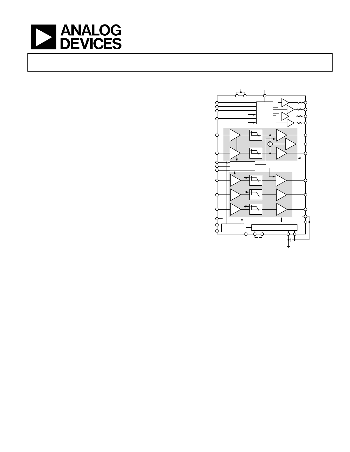
GENERAL DESCRIPTION
The ADA4424-6 is a high performance video reconstruction filter
specifically designed for consumer applications. It consists of a
standard definition (SD) section with two fifth-order Butterworth
filters and a high definition (HD) section with three fifth-order
filters. The SD section contains an internal Y/C summer for CVBS
output, whereas the HD section provides selectable corner
frequencies for either extended definition (ED) or HD signals.
The ADA4424-6 filter/buffer section operates from a single 3.3 V
supply. Full support for D-terminal (EIAJ RC-5237 D5) and S1/S2
signaling is provided, along with a dedicated 5 V supply pin.
Separate enable pins are provided for the SD and HD sections.
Charge Pump
ADA4424-6
FUNCTIONAL BLOCK DIAGRAM
D1
D2
D3
S
Y_IN
C_IN
MODE0
MODE1
FFSET_ENB
HY_IN
HPb_IN
HPr_IN
FC_SEL
SD_ENABLE
HD_ENABLE
The luma channels (Y_IN, HY_IN) of the ADA4424-6 are
capable of detecting and cancelling dc input offsets of up to
1.1 V. Four distinct modes of detection/cancellation are
available.
The output drivers on the ADA4424-6 feature rail-to-rail outputs
with 6.2 dB gain. An on-board charge pump allows the outputs to
swing up to 1.4 V below ground, eliminating the need for large
coupling capacitors. Each output is capable of driving two 75 Ω
doubly terminated cables.
The ADA4424-6 is available in a 38-lead TSSOP and operates in
the industrial temperature range of −40°C to +85°C.
+3.3
VDD3_SD VDD3_HD VDD5
HD_ENB
SD_ENB
×1
×1
OFFSET
CANCELLATION
FC_SEL
×1
FC_SEL
×1
FC_SEL
×1
HD_ENBSD_ENB
POWER
MANAGEMENT
+3.3V
+5V
D/S
TERMINAL
CONTROL
LPF
LPF
LPF
LPF
LPF
CHARGE PUM P
C1b C2/CP_OUTVDD3_CP GND_CP
C1a
C1
Figure 1.
L1
L2
L3
S1/S2
×2
×2
×2
ADA4424-6
×2
×2
×2
C2
L1_OUT
L2_OUT
L3_OUT
S1/S2_OUT
Y_OUT
CVBS_OUT
C_OUT
HY_OUT
HPb_OUT
HPr_OUT
VSS_SD
VSS_HD
08550-001
Rev. C
Information furnished by Analog Devices is believed to be accurate and reliable. However, no
responsibility is assumed by Analog Devices for its use, nor for any infringements of patents or other
rights of third parties that may result from its use. Specifications subject to change without notice. No
license is granted by implication or otherwise under any patent or patent rights of Analog Devices.
Trademarks and registered trademarks are the property of their respective owners.
One Technology Way, P.O. Box 9106, Norwood, MA 02062-9106, U.S.A.
Tel: 781.329.4700 www.analog.com
Fax: 781.461.3113 ©2009-2010 Analog Devices, Inc. All rights reserved.
Page 2

ADA4424-6
TABLE OF CONTENTS
Features .............................................................................................. 1
Applications ....................................................................................... 1
Functional Block Diagram .............................................................. 1
General Description ......................................................................... 1
Revision History ............................................................................... 2
Specifications ..................................................................................... 3
Absolute Maximum Ratings ............................................................ 6
Thermal Resistance ...................................................................... 6
Maximum Power Dissipation ..................................................... 6
ESD Caution .................................................................................. 6
Pin Configuration and Function Descriptions ............................. 7
REVISION HISTORY
07/10—Rev. B to Rev. C
Change to General Description Section ........................................ 1
05/10—Rev. A to Rev. B
Change to Table 1, Overall Performance ....................................... 3
Change to Ordering Guide ............................................................ 15
12/09—Rev. 0 to Rev. A
Changes to Table 1 ............................................................................ 4
Changes to Table 2 ............................................................................ 5
Changes to Table 5 .......................................................................... 10
Changes to Table 8 to Table 11 ...................................................... 11
Change to Table 12 and Table 13 .................................................. 12
10/09—Revision 0: Initial Version
Typical Performance Characteristics ..............................................9
Applications Information .............................................................. 11
CVBS Output .............................................................................. 11
Corner Frequency Selection ..................................................... 11
Input DC Offset Cancellation ................................................... 11
D-Terminal and S-Terminal Support ...................................... 12
Power-Down ............................................................................... 13
Charge Pump .............................................................................. 13
Printed Circuit Board (PCB) Layout ....................................... 13
Outline Dimensions ....................................................................... 15
Ordering Guide .......................................................................... 15
Rev. C | Page 2 of 16
Page 3

ADA4424-6
SPECIFICATIONS
V
= 3.3 V, TA = 25°C, VO = 2.042 V p-p, RL = 150 Ω, dc-coupled outputs, unless otherwise noted. Charge pump configured as shown in
DD3
Figure 18.
Table 1.
Parameter Test Conditions/Comments Min Typ Max Unit
OVERALL PERFORMANCE
DC Voltage Gain All channels 6.0 6.2 6.4 dB
Input Voltage Range, All Inputs Not including dc offset −0.6 to +1.4 V
Output Voltage Range, All Outputs −1.6 to +3.0 V
Input Bias Current Y_IN, HY_IN, dc-coupled 30 pA
Input Impedance C_IN, HPb_IN, HPr_IN, ac-coupled 800 kΩ
Output Resistance
L1_OUT, L2_OUT, L3_OUT, S1/S2_OUT, dc-coupled 10.5 kΩ
SD CHANNEL DYNAMIC PERFORMANCE
In-Band Peaking f = 100 kHz to 6.75 MHz 0.00 0.01 dB
1 dB Bandwidth 14 18 MHz
Out-of-Band Rejection f = 148.5 MHz 38 42 dB
Crosstalk f = 1 MHz 67 dB
Total Harmonic Distortion f = 1 MHz, VO = 1.4 V p-p 0.07 %
Signal-to-Noise Ratio f = 100 kHz to 6 MHz, unweighted 68 dB
Group Delay Variation f = 100 kHz to 5 MHz 1 ns
Differential Gain NTSC 0.2 %
Differential Phase NTSC 0.5 Degrees
ED CHANNEL DYNAMIC PERFORMANCE FC_SEL = low (0)
In-Band Peaking f = 100 kHz to 13.5 MHz 0.02 0.1 dB
1 dB Bandwidth 21 25 MHz
Out-of-Band Rejection f = 148.5 MHz 38 42 dB
Crosstalk f = 1 MHz 65 dB
Total Harmonic Distortion f = 5 MHz, VO = 1.4 V p-p 0.45 %
Signal-to-Noise Ratio f = 100 kHz to 13.5 MHz, unweighted 66 dB
Group Delay Variation f = 100 kHz to 13.5 MHz 1.5 ns
HD CHANNEL DYNAMIC PERFORMANCE FC_SEL = high (1)
In-Band Peaking f = 100 kHz to 30 MHz 0.1 0.2 dB
1 dB Bandwidth Y Channel (HY_OUT) 30 39 MHz
P Channels (HPb_OUT, HPr_OUT) 25 34 MHz
Out-of-Band Rejection f = 148.5 MHz 33 37 dB
Crosstalk f = 1 MHz 65 dB
Total Harmonic Distortion f = 10 MHz, VO = 1.4 V p-p 1.2 %
Signal-to-Noise Ratio f = 100 kHz to 30 MHz, unweighted 65 dB
Group Delay Variation f = 100 kHz to 30 MHz 2.2 ns
DC CHARACTERISTICS
Operating Voltage, 3.3 V Supply 3.14 to 3.46 V
Quiescent Supply Current, 3.3 V Supply
SD disabled, SD_ENABLE = low, HD_ENABLE = high 54 mA
HD disabled, SD_ENABLE = high, HD_ENABLE = low 45 mA
Both disabled, SD_ENABLE = low, HD_ENABLE = low 6.1 10 mA
Operating Voltage, 5 V Supply 4.75 to 5.25 V
Y_OUT, C_OUT, CVBS_OUT, HY_OUT, HPb_OUT,
HPr_OUT, dc-coupled
Both active, SD_ENABLE = high, HD_ENABLE = high,
no load, no signal, not including D/S terminal outputs
0.5 Ω
93 133 mA
Rev. C | Page 3 of 16
Page 4
ADA4424-6
Parameter Test Conditions/Comments Min Typ Max Unit
Quiescent Supply Current, 5 V Supply
SD_ENABLE = high, HD_ENABLE = high,
= 100 kΩ, D1, D2, D3 = high, S = high
R
L
SD_ENABLE = low, HD_ENABLE = low 5 15 μA
PSRR ED/HD channels, output referred −42 dB
SD channels, output referred −41 dB
DC Offset See Table 6 and Table 7
Input Referred, Offset Cancellation
OFFSET_ENB = low
Disabled Mode
SD Channels Y_IN = 0 V dc −60 −20 +60 mV
CVBS Channel Y_IN = 0 V dc −100 −40 +100 mV
ED/HD Channels HY_IN = 0 V dc −60 −20 +60 mV
Input Referred, Fixed Offset
OFFSET_ENB = high, MODE1 = high
Cancellation Mode
SD Fixed High Offset Mode Y_IN = 1.0 V dc, MODE0 = low −100 −30 +100 mV
ED/HD Fixed High Offset Mode HY_IN = 1.1 V dc, MODE0 = low −100 −38 +100 mV
SD Fixed Low Offset Mode Y_IN = 0.33 V dc, MODE0 = high −90 −17 +90 mV
ED/HD Fixed Low Offset Mode HY_IN = 0.33 V dc, MODE0 = high −100 −25 +100 mV
Input Referred, Auto Offset
OFFSET_ENB = high, MODE1 = low
Cancellation Mode
SD Auto Offset Mode
Y_IN = 0 V to 1.0 V dc, MODE0 = low −70 −36 +70 mV
Sync Tip Sampling
ED/HD Auto Offset Mode
HY_IN = 0 V to 1.1 V dc, MODE0 = low −95 −46 +95 mV
Sync Tip Sampling
SD Auto Offset Mode
Y_IN = 0 V to 1.0 V dc, MODE0 = high −25 −6 +25 mV
Back Porch Sampling
ED/HD Auto Offset Mode
HY_IN = 0 V to 1.1 V dc, MODE0 = high −25 −5 +25 mV
Back Porch Sampling
FC_SEL Input Logic Low Level 0 0.6 V
FC_SEL Input Logic High Level 1.2 V
xD_ENABLE, OFFSET_ENB, MODEx
0 0.8 V
Input Logic Low Level
xD_ENABLE, OFFSET_ENB, MODEx
2.0 V
Input Logic High Level
xD_ENABLE Assert Time xD_ENABLE = low to high 95 ns
xD_ENABLE Deassert Time xD_ENABLE = high to low 20 ns
xD_ENABLE Input Bias Current Disabled, xD_ENABLE = low 6.1 μA
Input-to-Output Isolation Disabled, xD_ENABLE = low, f = 5 MHz −100 dB
= 100 kΩ 0 0.6 V
D- and S-Terminal Input Logic
R
L
Low Level
= 100 kΩ 0.9 1.9 V
D- and S-Terminal Input Logic
R
L
Mid Level
= 100 kΩ 2.7 V
D- and S-Terminal Input Logic
R
L
High Level
= 100 kΩ 200 kΩ
D- and S-Terminal Input Logic Open
R
L
(Hi-Z) Resistance Value
V
D-Terminal (L1_OUT, L2_OUT, L3_OUT)
= 5.0 V, RL = 100 kΩ, D1, D2, D3 = low 0.0 V
DD5
Low Level Output
= 5.0 V, RL = 100 kΩ, D1, D3 = mid or open 2.1 V
D-Terminal (L1_OUT, L3_OUT) Mid
V
DD5
Level Output
= 5.0 V, RL = 100 kΩ, D1, D2, D3 = high 4.5 V
D-Terminal (L1_OUT, L2_OUT, L3_OUT)
V
DD5
High Level Output
V
S-Terminal (S1/S2_OUT) Low Level
= 5.0 V, RL = 100 kΩ, S = low 0.0 V
DD5
Output
190 200 μA
V
DD3
V
DD3
V
DD3
Rev. C | Page 4 of 16
Page 5
ADA4424-6
Parameter Test Conditions/Comments Min Typ Max Unit
= 5.0 V, RL = 100 kΩ, S = mid or open 2.1 V
S-Terminal (S1/S2_OUT) Mid Level
Output
S-Terminal (S1/S2_OUT) High Level
Output
CHARGE PUMP CHARACTERISTICS
Output Voltage −1.66 V
Output Voltage Ripple 180 mV p-p
Output Ripple Frequency 100 kHz
V
DD5
V
= 5.0 V, RL = 100 kΩ, S = high 4.5 V
DD5
All channels operating; C1 = C2 = 4.7 μF, C3 = C4 =
1.0 μF, R1 = 1 Ω (see Figure 18)
Rev. C | Page 5 of 16
Page 6

ADA4424-6
ABSOLUTE MAXIMUM RATINGS
Table 2.
Parameter Rating
3.3 V Supply Voltage 3.6 V
5 V Supply Voltage 5.5 V
Digital Input Voltage (Pin 2 to Pin 5, Pin 8,
3.6 V
Pin 12, Pin 15, Pin 16, Pin 23)
Power Dissipation See Figure 2
Storage Temperature Range −65°C to +125°C
Operating Temperature Range −40°C to +85°C
Lead Temperature (Soldering, 10 sec) 300°C
Junction Temperature 150°C
Stresses above those listed under Absolute Maximum Ratings
may cause permanent damage to the device. This is a stress
rating only; functional operation of the device at these or any
other conditions above those indicated in the operational
section of this specification is not implied. Exposure to absolute
maximum rating conditions for extended periods may affect
device reliability.
THERMAL RESISTANCE
θJA is specified for the device soldered to a high thermal
conductivity 4-layer (2s2p) circuit board, as described in
EIA/JESD 51-7.
Table 3.
Package Type θJA θJC Unit
38-Lead TSSOP 67.6 14.0 °C/W
The power dissipated in the package (P
quiescent power dissipation and the power dissipated in the
package due to the load drive for all outputs. The quiescent
power is the voltage between the supply pins (V
quiescent current (I
depends on the particular application. For each output, the
power due to load drive is calculated by multiplying the load
current by the associated voltage drop across the device. The
power dissipated due to the loads is equal to the sum of the
power dissipations due to each individual load. RMS voltages
and currents must be used in these calculations.
Airflow increases heat dissipation, effectively reducing θ
Figure 2 shows the maximum power dissipation in the package
vs. the ambient temperature for the 38-lead TSSOP (67.6°C/W)
on a JEDEC standard 4-layer board. θ
2.4
2.2
2.0
1.8
1.6
1.4
1.2
1.0
0.8
0.6
0.4
MAXIMUM POWER DISSIPATION (W)
0.2
0
0 100
10 20 30 40 50 60 70 80 90
MAXIMUM POWER DISSIPATION
The maximum safe power dissipation in the ADA4424-6
package is limited by the associated rise in junction temperature
(T
) on the die. At approximately 150°C, which is the glass
J
transition temperature, the plastic changes its properties. Even
temporarily exceeding this temperature limit can change the
stresses that the package exerts on the die, permanently shifting
the parametric performance of the ADA4424-6. Exceeding a
junction temperature of 150°C for an extended time can result
in changes in the silicon devices, potentially causing failure.
ESD CAUTION
). The power dissipated due to load drive
S
AMBIENT TEMPERATURE (°C)
Figure 2. Maximum Power Dissipation vs.
Ambient Temperature for a 4-Layer Board
) is the sum of the
D
) times the
S
JA
values are approximate.
JA
.
08550-002
Rev. C | Page 6 of 16
Page 7

ADA4424-6
PIN CONFIGURATION AND FUNCTION DESCRIPTIONS
GND5
D1
D2
D3
Y_IN
VDD3_SD
SD_ENABLE
C_IN
GND3
HY_IN
FC_SEL
HPb_IN
HPr_IN
HD_ENABLE
MODE0
OFFSET_ENB
VDD3_CP
C1a
1
2
3
4
5
S
6
ADA4424-6
7
TOP VIEW
8
(Not to Scale)
9
10
11
12
13
14
15
16
17
18
19 20
38
VDD5
37
L1_OUT
36
L2_OUT
35
L3_OUT
34
S1/S2_OUT
33
Y_OUT
32
VSS_SD
31
CVBS_OUT
30
C_OUT
29
GND3
28
HY_OUT
27
VSS_HD
26
HPb_OUT
25
HPr_OUT
24
VDD3_HD
23
MODE1
22
C2/CP_OUT
21
C1b
GND_CP
08550-003
Figure 3. Pin Configuration, Top View
Table 4. Pin Function Descriptions
Pin No. Mnemonic Description
1 GND5 Ground Pin for 5 V Supply.
2 D1 D-Terminal Vertical Resolution Selection Input.
3 D2 D-Terminal Scan Selection Input.
4 D3 D-Terminal Aspect Ratio Selection Input.
5 S S-Terminal Aspect Ratio Selection Input.
6 Y_IN SD Luma (Y) Input.
7 VDD3_SD 3.3 V Supply Pin for SD Filter Section.
8 SD_ENABLE Output Enable Pin for SD (Y, C, CVBS).
9 C_IN SD Chroma (C) Input.
10, 29 GND3 Ground Pins for 3.3 V Supply.
11 HY_IN ED/HD Y Component Input.
12 FC_SEL Filter Corner Frequency Selection Pin for HY, HPb, HPr Channels.
13 HPb_IN ED/HD Pb Component Input.
14 HPr_IN ED/HD Pr Component Input.
15 HD_ENABLE Output Enable Pin for ED/HD (HY, HPb, HPr).
16 MODE0
This pin selects sync tip or back porch sampling when MODE1 = 0 and selects high or low fixed offset
subtraction when MODE1 = 1.
17 OFFSET_ENB Offset Cancellation Enable Pin.
18 VDD3_CP 3.3 V Supply Pins for Charge Pump Section.
19, 21 C1a, C1b Charge Pump Capacitor C1 Connection Pin.
20 GND_CP Ground Pin for 3.3 V Charge Pump Supply.
22 C2/CP_OUT Charge Pump Output Pin. Connect Capacitor C2 from this pin to ground.
23 MODE1 Selects Automatic or Fixed Offset Subtraction Mode.
24 VDD3_HD 3.3 V Supply Pin for ED/HD Filter Section.
25 HPr_OUT ED/HD Pr Component Output.
26 HPb_OUT ED/HD Pb Component Output.
27 VSS_HD
Negative Supply Pin for ED/HD Filter Section. This pin should be connected to the charge pump output
(Pin 22), as shown in Figure 18.
28 HY_OUT ED/HD Y Component Output.
30 C_OUT SD Chroma (C) Output.
31 CVBS_OUT SD Composite Video (CVBS) Output.
Rev. C | Page 7 of 16
Page 8

ADA4424-6
Pin No. Mnemonic Description
32 VSS_SD
33 Y_OUT SD Luma (Y) Output.
34 S1/S2_OUT S-Terminal Aspect Ratio Selection Output.
35 L3_OUT D-Terminal Aspect Ratio Selection Output.
36 L2_OUT D-Terminal Scan Selection Output.
37 L1_OUT D-Terminal Vertical Resolution Selection Output.
38 VDD5 5 V Supply Pin for D-Terminal and S-Terminal Signaling.
Negative Supply Pin for SD Filter Section. This pin should be connected to the charge pump output (Pin 22), as
shown in Figure 18.
Rev. C | Page 8 of 16
Page 9

ADA4424-6
TYPICAL PERFORMANCE CHARACTERISTICS
V
= 3.3 V, TA = 25°C, VO = 2.042 V p-p, RL = 150 Ω, dc-coupled outputs, unless otherwise noted. Charge pump configured as shown in
DD3
Figure 18.
10
0
0.5
–10
–20
–30
–40
NORMALIZED GAIN (dB)
–50
–60
0.1
110100
FREQUENCY (MHz)
Y
C
CVBS
08550-004
Figure 4. Frequency Response—SD Channels
10
0
–10
–20
–30
–40
NORMALIZED GAIN (dB)
–50
Pr
HY Pb
0
Y/CVBS
–0.5
NORMALIZED GAIN (dB)
–1.0
0.1 100
110
FREQUENCY (MHz)
C
Figure 7. Frequency Response Peaking—SD Channels
0.5
Pb
0
–0.5
NORMALIZED GAIN (dB)
HY
Pr
08550-007
–60
0.1 1k
1 10 100
FREQUENCY (MHz)
Figure 5. Frequency Response—ED Channels
10
0
–10
–20
–30
–40
NORMALIZED GAIN (dB)
–50
–60
0.1 1k
1 10 100
FREQUENCY (MHz)
HY
Figure 6. Frequency Response—HD Channels
–1.0
0.1 100
08550-005
110
FREQUENCY (MHz)
08550-008
Figure 8. Frequency Response Peaking—ED Channels
0.5
HY
0
Pr
Pb
08550-006
–0.5
NORMALIZED GAIN (dB)
–1.0
0.1 100
110
FREQUENCY (MHz)
Pb/Pr
08550-009
Figure 9. Frequency Response Peaking—HD Channels
Rev. C | Page 9 of 16
Page 10

ADA4424-6
–
–
–
20
ALL HOST ILE
REFERRED TO INPUT
–30
20
ALL HOSTILE
REFERRED TO INP UT
–30
–40
–50
C_OUT
CROSSTALK (dB)
–60
Y_OUT
–70
CVBS_OUT
–80
0.1 100
110
FREQUENCY (MHz)
Figure 10. Crosstalk—SD Channels
45
40
35
30
25
20
15
GROUP DELAY (ns)
10
5
0
0.1 100
CVBS_OUT
Y_OUT, C_OUT
110
FREQUENCY (MHz)
Figure 11. Group Delay—SD Channels
–40
–50
CROSSTALK (dB)
–60
HPb_OUT, HPr_OUT
–70
HY_OUT
–80
0.1 100
08550-010
110
FREQUENCY (MHz)
08550-013
Figure 13. Crosstalk—ED and HD Channels
45
40
35
30
25
20
15
GROUP DELAY (ns)
10
5
0
0.1 100
08550-011
110
FREQUENCY (MHz)
08550-014
Figure 14. Group Delay—ED Channels
45
40
35
30
25
20
15
GROUP DELAY (ns)
10
5
0
0.1 100
110
FREQUENCY (MHz)
Figure 12. Group Delay—HD Channels
08550-012
40
VIN = 1.0V p-p
R
= 150
L
–50
SD_ENABLE = 0
HD_ENABLE = 0
–60
–70
–80
–90
–100
INPUT-TO-OUTPUT ISOLATION (dB)
–110
–120
0.1 100
110
FREQUENCY (MHz)
Figure 15. Input-to-Output Isolation—All Channels
08550-015
Rev. C | Page 10 of 16
Page 11

ADA4424-6
APPLICATIONS INFORMATION
CVBS OUTPUT
The composite video signal (CVBS_OUT) is produced by
passively summing the Y and C channels (see Figure 1), after
amplification by their respective gain stages. Each signal
experiences a 6.2 dB loss from the passive summation and is
subsequently amplified by 6.2 dB in the fixed stage following
the summer. The net signal gain through the composite video
path is, therefore, 0 dB, and the resulting composite signal
present at the ADA4424-6 output is the sum of Y and C with
unity gain.
CORNER FREQUENCY SELECTION
The component channels of the ADA4424-6 allow for a 1 dB
filter corner frequency of either 25 MHz or 39 MHz/34 MHz.
The FC_SEL pin operates as described in Ta b l e 5.
Table 5. ED/HD Bandwidth Selection
FC_SEL (Pin 12) HD/ED −1 dB Corner Frequency (Typ)
Low (0) ED 25 MHz
High (1) HD 39 MHz (HY); 34 MHz (Pb, Pr)
BACK PORCH SAMPLE INTERVAL
SYNC TIP SAMPLE INTERVAL
Figure 16. Back Porch and Sync Tip Sample Intervals (SD/ED)
BLACK LEVEL
8550-017
INPUT DC OFFSET CANCELLATION
The luma channels (Y_IN, HY_IN) of the ADA4424-6 are capable
of detecting and cancelling dc input offsets of up to 1.1 V. Four
distinct modes of detection/cancellation are available. These are
selected via the MODE1 and MODE0 pins. The chroma (C_IN)
and color difference (HPb_IN, HPr_IN) inputs do not support
offset cancellation. It is recommended that these inputs be accoupled.
Automatic Detection/Cancellation Mode
There are two modes of automatic operation. The primary mode
samples the input signal between the rising edge of the horizontal sync pulse and the start of active video (back porch), averages
the value over the sampling interval, and subtracts it from the
output signal. This is the more accurate method and is able to
reduce the input-referred offsets to less than 25 mV.
An alternate method is available for copy-protected signals, where
sampling the back porch may not provide a reliable dc average.
This method detects the input negative sync tip, and clamps it
to a fixed value (−214 mV for SD, and −300 mV for ED/HD).
Sample intervals for SD and ED are shown in Figure 16, and
the HD sample intervals are shown in Figure 17.
BLACK LEVEL
BACK PORCH SAMPLE INTERVAL
SYNC TIP SAMP LE INTERVAL
Figure 17. Back Porch and Sync Tip Sample Intervals (HD)
08550-018
Rev. C | Page 11 of 16
Page 12

ADA4424-6
Fixed Offset Cancellation Mode
In addition to the automatic mode, there are two levels of fixed
offset correction available. In high offset mode, fixed voltages of
1.0 V and 1.1 V are subtracted from the Y_IN and HY_IN inputs,
respectively. In low offset mode, a fixed voltage of 0.33 V is
subtracted from both Y_IN and HY_IN. The various modes of
offset cancellation are outlined in Ta b le 6 .
Table 6. Offset Cancellation Mode Selection
MODE1
(Pin 23)
Low (0) Low (0)
Low (0) High (1)
High (1) Low (0)
High (1) High (1) Fixed cancellation mode, low dc offset.
MODE0
(Pin 16) Output Offset Cancellation
Auto-cancel, sync-tip sampling mode.
Clamps the input referred SD sync tip
to −214 mV, and the input referred
ED/HD sync tip to −300 mV.
Auto-cancel, back porch sampling
mode. Sets the output blanking level
to 0 V, independent of sync depth.
Fixed cancellation mode, high dc
offset.
Subtracts 1.0 V from the Y_IN signal;
subtracts 1.1 V from the HY_IN signal.
Subtracts 0.33 V from both the Y_IN
and HY_IN signals.
Offset Cancellation Disable
The offset cancellation function can be enabled or disabled via
the OFFSET_ENB pin, as described in Ta ble 7 .
D-TERMINAL AND S-TERMINAL SUPPORT
Full D-terminal support (EIAJ RC-5237 D5) is provided for the
component channels (HY_OUT, HPb_OUT, HPr_OUT). Level
D1 through Level D5 are supported for vertical resolution, scan
type, and aspect ratio selection. Details are shown in Table 8,
Tabl e 9, and Ta b l e 10 .
S-terminal (also known as S_DC or S1/S2) support for S-video
aspect ratio selection is also provided, as described in Table 1 1.
The VDD5 pin (Pin 38) provides 5 V power for these outputs.
If D- or S-terminal support is not required, it is recommended
that Pin 2 to Pin 5 and Pin 34 to Pin 38 remain unconnected.
Table 8. D-Terminal Control for Vertical Resolution Selection
Nominal Output (V)
Input Logic
Level D1 (Pin 2)
Low (0) 0.0 480
Mid or open 2.1 720
High (1) 4.5 1080
L1_OUT (Pin 37)
= 100 kΩ
R
L
Table 9. D-Terminal Control for Scan Selection
Nominal Output (V)
Input Logic Level
D2 (Pin 3)
Low (0) 0.0 Interlaced
Mid or open 2.1 N/A
High (1) 4.5 Progressive
L2_OUT (Pin 36)
= 100 kΩ Scan Type
R
L
Vertical Resolution
(Number of Lines)
Table 7. Offset Cancellation Enable/Disable
OFFSET_ENB
(Pin 17) Offset Cancellation State
Low (0) Offset cancellation is disabled.
High (1)
Offset cancellation is enabled. Function is
determined by the MODE1 and MODE0 pins
(see Tab le 6).
Table 10. D-Terminal Control for Aspect Ratio Selection
Nominal Output (V)
Input Logic Level
D3 (Pin 4)
Low (0) 0.0 4:3
Mid or open 2.1 4:3 letterbox
High (1) 4.5 16:9
L3_OUT (Pin 35)
= 100 kΩ Aspect Ratio
R
L
Table 11. S-Terminal Control for Aspect Ratio Selection
Nominal Output (V)
Input Logic Level
S (Pin 5)
Low (0) 0.0 4:3
Mid or open 2.1 4:3 letterbox
High (1) 4.5 16:9
S1/S2_OUT (Pin 34)
RL = 100 kΩ
Aspect Ratio
Rev. C | Page 12 of 16
Page 13

ADA4424-6
POWER-DOWN
The ADA4424-6 provides separate output enable pins for the
SD and ED/HD sections. In addition to powering down the Y,
C, and CVBS outputs, the SD_ENABLE pin, when driven low,
also places the S1/S2 output (S1/S2_OUT, Pin 34) in a high
impedance state. Likewise, driving the HD_ENABLE pin low
disables the component outputs (HY_OUT, HPb_OUT, and
HPr_OUT) and changes the L1, L2, and L3 outputs (Lx_OUT,
Pin 35 to Pin 37) to a high impedance state. Control details are
shown in Tab l e 12 and Ta ble 1 3.
Table 12. Power-Down Control for SD Channels
SD_ENABLE
(Pin 8)
Low (0) Disabled High-Z (Open)
High (1) Enabled Active
Table 13. Power-Down Control for ED/HD Channels
HD_ENABLE
(Pin 15)
Low (0) Disabled High-Z (Open)
High (1) Enabled Active
SD Outputs
(Y, C, CVBS)
ED/HD Outputs
(HY, HPb, HPr)
S1/S2_OUT
(Pin 34)
Lx_OUT (Pin 35,
Pin 36, Pin 37)
CHARGE PUMP
The ADA4424-6 features an on-chip charge pump that supplies
a negative rail voltage for the output stages. To minimize internal
noise coupling, the charge pump uses an external connection to
the negative supply pins (VSS_SD and VSS_HD). These pins
should be connected to the C2/CP_OUT pin, each decoupled
with a 1.0 μF capacitor. It is also recommended to place a small
(1 Ω) series resistor in this connection. This forms a low-pass
filter with the VSS decoupling capacitors and further reduces
coupled noise. The charge pump also requires two 4.7 μF ceramic
capacitors, one connected across the C1a and C1b pins, and one
connected from the C2/CP_OUT pin to ground. The recommended charge pump configuration is shown in the application
diagram (Figure 18).
With the black or zero level of the outputs placed at approximately ground potential, the outputs can swing up to 1.6 V in
the negative direction. This eliminates the need for large output
coupling capacitors because the input-referred dc offsets does not
exceed ±100 mV (depending on the selected cancellation mode).
PRINTED CIRCUIT BOARD (PCB) LAYOUT
As with all high speed applications, attention to the PCB layout
is of paramount importance. When designing with the ADA4424-6,
adhere to standard high speed layout practices. A solid ground
plane is recommended, and surface-mount, ceramic power supply
decoupling capacitors should be placed as close as possible to the
supply pins. Connect all of the ADA4424-6 GND pins to the
ground plane with traces that are as short as possible. Controlled
impedance traces of the shortest length possible should be used
to connect to the signal I/O pins and should not pass over any
voids in the ground plane. A 75 Ω impedance level is typically
used in video applications. When driving transmission lines,
include series termination resistors on the signal outputs of the
ADA4424-6.
Rev. C | Page 13 of 16
Page 14

ADA4424-6
V
VIDEO ENCODE R
DAC1
DAC2
DAC3
DAC4
DAC5
RSET2RSET1
10µF
+3.3
+
OFFSET_ENB
100nF
1.0µF
1.0µF
MODE0
MODE1
Y_IN
C_IN
SD_ENABLE
VDD3_SD
1.0µF
HY_IN
HPb_IN
HPr_IN
FC_SEL
HD_ENABLE
VDD3_HD
1.0µF
VDD3_CP
1.0µF
ADA4424-6
x1
x1
LPF
LPF
LPF
LPF
LPF
CHARGE PUMP
x2
x2
x2
x2x1
x2x1
x2x1
Y_OUT
CVBS_OUT
C_OUT
GND3
VSS_SD
C3
1.0µF
HY_OUT
HPb_OUT
HPr_OUT
GND3
VSS_HD
C4
1.0µF
75
75
75
75
75
CVBS
S-VIDEO
75
Y
Pb
Pr
+3.3V
C1a C1b
C1
4.7µF
GND_CP C2/CP_OUT
C2
4.7µF
R1
1.0
Figure 18. Typical Application Diagram for Using the ADA4424-6 in Auto Offset Cancellation Mode
(D and S Terminal Connections Not Shown)
08550-019
Rev. C | Page 14 of 16
Page 15

ADA4424-6
0
0
OUTLINE DIMENSIONS
9.80
9.70
9.60
38
PIN 1
.15
.05
COPLANARITY
0.10
0.50
BSC
COMPLIANT TO JEDEC STANDARDS MO-153-BD-1
0.27
0.17
20
191
SEATING
PLANE
1.20
MAX
4.50
4.40
4.30
0.20
0.09
6.40 BSC
8°
0°
0.70
0.60
0.45
Figure 19. 38-Lead Thin Shrink Small Outline Package [TSSOP]
(RU-38)
Dimensions shown in millimeters
ORDERING GUIDE
Package
Model1 Temperature Range Package Description
Option
ADA4424-6ARUZ −40°C to +85°C 38-Lead Thin Shrink Small Outline Package (TSSOP) RU-38 50
ADA4424-6ARUZ-R7 −40°C to +85°C 38-Lead Thin Shrink Small Outline Package (TSSOP) RU-38 1,000
ADA4424-6ARUZ-RL −40°C to +85°C 38-Lead Thin Shrink Small Outline Package (TSSOP) RU-38 2,500
1
Z = RoHS Compliant Part.
Ordering
Quantity
Rev. C | Page 15 of 16
Page 16

ADA4424-6
NOTES
©2009-2010 Analog Devices, Inc. All rights reserved. Trademarks and
registered trademarks are the property of their respective owners.
D08550-0-7/10(C)
Rev. C | Page 16 of 16
 Loading...