www.BDTIC.com/ADI
Low Cost 6-Channel HD/SD Video Filter
FEATURES FEATURES
Sixth-order filters Sixth-order filters
Transparent input sync tip clamp Transparent input sync tip clamp
−1 dB bandwidth of 26 MHz typical for HD −1 dB bandwidth of 26 MHz typical for HD
HD rejection @ 75 MHz: 48 dB typical HD rejection @ 75 MHz: 48 dB typical
NTSC differential gain: 0.19% NTSC differential gain: 0.19%
NTSC differential phase: 0.76° NTSC differential phase: 0.76°
Rail-to-rail outputs Rail-to-rail outputs
Low quiescent current: 32 mA typical Low quiescent current: 32 mA typical
Disable feature Disable feature
Output dc offset Output dc offset
APPLICATIONS APPLICATIONS
Set-top boxes Set-top boxes
DVD players and recorders DVD players and recorders
HDTVs HDTVs
Projectors Projectors
Personal video recorders Personal video recorders
GENERAL DESCRIPTION GENERAL DESCRIPTION
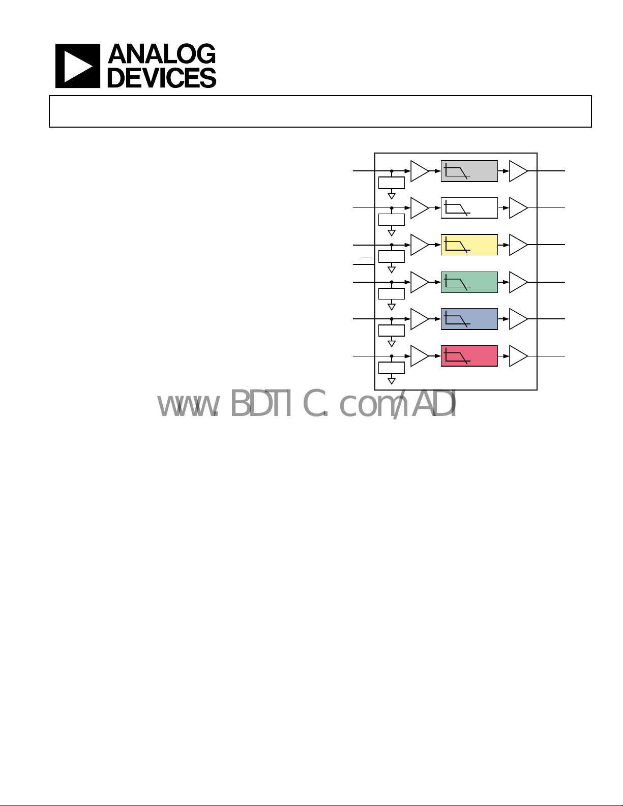
The ADA4420-6 is a low cost video reconstruction filter specifically
The ADA4420-6 is a low cost video reconstruction filter specifically
designed for consumer applications. It consists of six independent
designed for consumer applications. It consists of six independent
sixth-order Butterworth filters/buffers, three for standard
sixth-order Butterworth filters/buffers, three for standard
definition (Y/C or CVBS) and three for high definition
definition (Y/C or CVBS) and three for high definition
component signals (YPbPr or RGB).
component signals (YPbPr or RGB).
The ADA4420-6 operates from a single 5 V supply and has a
The ADA4420-6 operates from a single 5 V supply and has a
low quiescent current of 32 mA, making it ideal for applications
low quiescent current of 32 mA, making it ideal for applications
where power consumption is critical. A disable feature allows
where power consumption is critical. A disable feature allows
for further power conservation by reducing the supply current
for further power conservation by reducing the supply current
to less than 8 µA typical when the device is not in use.
to less than 8 µA typical when the device is not in use.
ADA4420-6
FUNCTIONAL BLOCK DIAGRAM FUNCTIONAL BLOCK DIAGRAM
INSD1
INSD2
INSD3
DIS
INHD1
INHD2
INHD3
CLAMP
CLAMP
CLAMP
CLAMP
CLAMP
CLAMP
×1
×1
×1
×1
×1
×1
Figure 1.
SD
SD
SD
HD
HD
HD
ADA4420-6
Each channel features a transparent sync tip clamp, allowing ac
coupling of the inputs without requiring dc restoration.
The output drivers on the ADA4420-6 have rail-to-rail output
capabilities with 6 dB gain. A built-in offset of 250 mV allows
the outputs to be dc-coupled, eliminating the need for large
coupling capacitors. Each output is capable of driving two 75 Ω
doubly terminated cables.
The ADA4420-6 is available in a 16-lead QSOP and operates in
the extended industrial temperature range of −40°C to +85°C.
OUTSD1
×2
OUTSD2
×2
OUTSD3
×2
OUTHD1
×2
OUTHD2
×2
OUTHD3
×2
07532-001
Rev. 0
Information furnished by Analog Devices is believed to be accurate and reliable. However, no
responsibility is assumed by Analog Devices for its use, nor for any infringements of patents or other
rights of third parties that may result from its use. Specifications subject to change without notice. No
license is granted by implication or otherwise under any patent or patent rights of Analog Devices.
Trademarks and registered trademarks are the property of their respective owners.
One Technology Way, P.O. Box 9106, Norwood, MA 02062-9106, U.S.A.
Tel: 781.329.4700 www.analog.com
Fax: 781.461.3113 ©2008 Analog Devices, Inc. All rights reserved.

ADA4420-6
www.BDTIC.com/ADI
TABLE OF CONTENTS
Features .............................................................................................. 1
Applications ....................................................................................... 1
General Description ......................................................................... 1
Functional Block Diagram .............................................................. 1
Revision History ............................................................................... 2
Specifications ..................................................................................... 3
Absolute Maximum Ratings ............................................................ 4
Thermal Resistance ...................................................................... 4
Maximum Power Dissipation ..................................................... 4
ESD Caution .................................................................................. 4
Pin Configuration and Function Descriptions ............................. 5
REVISION HISTORY
8/08—Revision 0: Initial Version
Typical Performance Characteristics ..............................................6
Test Circuits ........................................................................................9
Applications Information .............................................................. 10
Overview ..................................................................................... 10
Disable ......................................................................................... 10
Input and Output Coupling ...................................................... 10
Printed Circuit Board (PCB) Layout ....................................... 10
Video Encoder Reconstruction Filter ...................................... 10
Outline Dimensions ....................................................................... 12
Ordering Guide .......................................................................... 12
Rev. 0 | Page 2 of 12

ADA4420-6
www.BDTIC.com/ADI
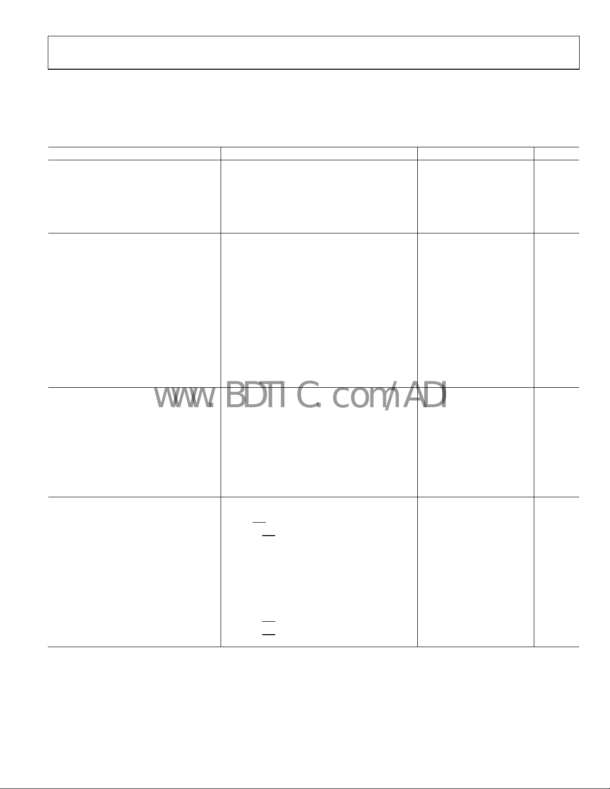
SPECIFICATIONS
VS = 5 V, TA = 25°C, VO = 2.0 V p-p, RL = 150 Ω, dc-coupled inputs, ac-coupled outputs, unless otherwise noted. See Figure 17, Figure 18,
and Figure 19 for the test circuits.
Table 1.
Parameter Test Conditions/Comments Min Typ Max Unit
OVERALL PERFORMANCE
DC Voltage Gain All channels 5.8 6.0 6.2 dB
Input Voltage Range, All Inputs 0 to 2.1 V
Output Voltage Range, All Outputs 0.25 to 4.6 V
Linear Output Current per Channel 30 mA
Filter Input Bias Current 1 μA
SD CHANNEL DYNAMIC PERFORMANCE
−1 dB Bandwidth 8.6 MHz
−3 dB Bandwidth 8.5 10 MHz
Out-of-Band Rejection f = 27 MHz 42 45 dB
Crosstalk f = 1 MHz −68 dB
Total Harmonic Distortion f = 1 MHz, VO = 1.4 V p-p, dc-coupled outputs 0.02 %
Signal-to-Noise Ratio f = 100 kHz to 6 MHz, unweighted 70 dB
Propagation Delay 57 ns
Group Delay Variation f = 100 kHz to 5 MHz 16 ns
Differential Gain
Differential Phase
HD CHANNEL DYNAMIC PERFORMANCE
−1 dB Bandwidth 26 MHz
−3 dB Bandwidth 27 31 MHz
Out-of-Band Rejection f = 75 MHz 43 48 dB
Crosstalk f = 1 MHz −68 dB
Total Harmonic Distortion f = 10 MHz, VO = 1.4 V p-p, dc-coupled outputs 0.57 %
Signal-to-Noise Ratio f = 100 kHz to 30 MHz, unweighted 66 dB
Propagation Delay 15 ns
Group Delay Variation f = 100 kHz to 30 MHz 11 ns
DC CHARACTERISTICS
Operating Voltage 4.75 to 5.25 V
Quiescent Supply Current
PSRR HD channel, referred to output 35 41 dB
SD channel, referred to output 40 45 dB
Output DC Offset All channels 135 250 375 mV
DISABLE Assert Voltage 1.9 V
DISABLE Assert Time 20 ns
DISABLE De-Assert Time 450 ns
DISABLE Input Bias Current
Input-to-Output Isolation
NTSC; ac-coupled inputs, dc-coupled outputs;
see Figure 18
NTSC; ac-coupled inputs, dc-coupled outputs;
see Figure 18
Active, DIS
Disabled, DIS
Disabled, DIS
Disabled, DIS
= 1
= 0
= 0
= 0, f = 5 MHz
0.19 %
0.76 Degrees
32 36 mA
7 13 μA
−6.8 μA
−96 dB
Rev. 0 | Page 3 of 12

ADA4420-6
www.BDTIC.com/ADI
ABSOLUTE MAXIMUM RATINGS
Table 2.
Parameter Rating
Supply Voltage 5.5 V
Power Dissipation See Figure 2
Storage Temperature Range −65°C to +125°C
Operating Temperature Range −40°C to +85°C
Lead Temperature (Soldering, 10 sec) 300°C
Junction Temperature 150°C
Stresses above those listed under Absolute Maximum Ratings
may cause permanent damage to the device. This is a stress
rating only; functional operation of the device at these or any
other conditions above those indicated in the operational
section of this specification is not implied. Exposure to absolute
maximum rating conditions for extended periods may affect
device reliability.
THERMAL RESISTANCE
θJA is specified for the device soldered to a high thermal
conductivity 4-layer (2s2p) circuit board, as described in
EIA/JESD 51-7.
Table 3.
Package Type θJA θJC Unit
16-Lead QSOP 105 23 °C/W
MAXIMUM POWER DISSIPATION
The maximum safe power dissipation in the ADA4420-6
package is limited by the associated rise in junction temperature
(T
) on the die. At approximately 150°C, which is the glass
J
transition temperature, the plastic changes its properties. Even
temporarily exceeding this temperature limit can change the
stresses that the package exerts on the die, permanently shifting
the parametric performance of the ADA4420-6. Exceeding a
junction temperature of 150°C for an extended time can result
in changes in the silicon devices, potentially causing failure.
The power dissipated in the package (P
) is the sum of the
D
quiescent power dissipation and the power dissipated in the
package due to the load drive for all outputs. The quiescent
power is the voltage between the supply pins (V
quiescent current (I
). The power dissipated due to load drive
S
) times the
S
depends on the particular application. For each output, the
power due to load drive is calculated by multiplying the load
current by the associated voltage drop across the device. The
power dissipated due to the loads is equal to the sum of the
power dissipations due to each individual load. RMS voltages
and currents must be used in these calculations.
Airflow increases heat dissipation, effectively reducing θ
.
JA
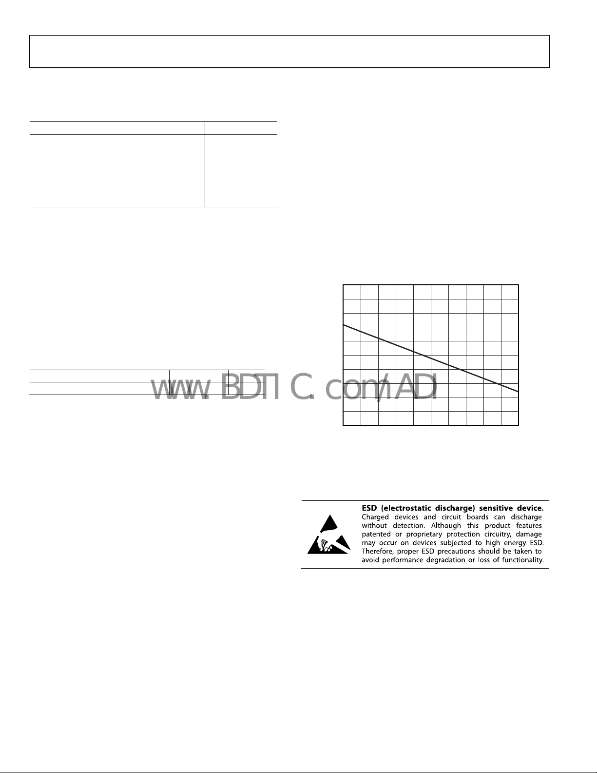
Figure 2 shows the maximum power dissipation in the package
vs. the ambient temperature for the 16-lead QSOP (105°C/W)
on a JEDEC standard 4-layer board. θ
2.0
1.8
1.6
1.4
1.2
1.0
0.8
0.6
0.4
MAXIMUM POWER DISSIPATION (W )
0.2
0
0 102030405060708090100
AMBIENT TEMPERATURE (°C)
Figure 2. Maximum Power Dissipation vs.
Ambient Temperature for a 4-Layer Board
values are approximate.
JA
07532-016
ESD CAUTION
Rev. 0 | Page 4 of 12
 Loading...