

Integrated Triple Video Filter
www.BDTIC.com/ADI
FEATURES
Optimized for high definition video
Sixth-order Butterworth filters
−1 dB bandwidth of 38 MHz
44 dB rejection at 75 MHz
5 ns group delay variation
Fixed throughput gain of ×2
0.06% differential gain
0.21° differential phase
Pin selectable output offset (DCO)
Single-supply operation
3.3 V to 5 V range
Rail-to-rail output
Output ESD protection exceeds 8 kV
Small packaging: 10-lead MSOP
APPLICATIONS
Set-top boxes
HDTVs
Projectors
DVD players/recorders
Personal video recorders
GENERAL DESCRIPTION
for High Definition Video
ADA4417-3
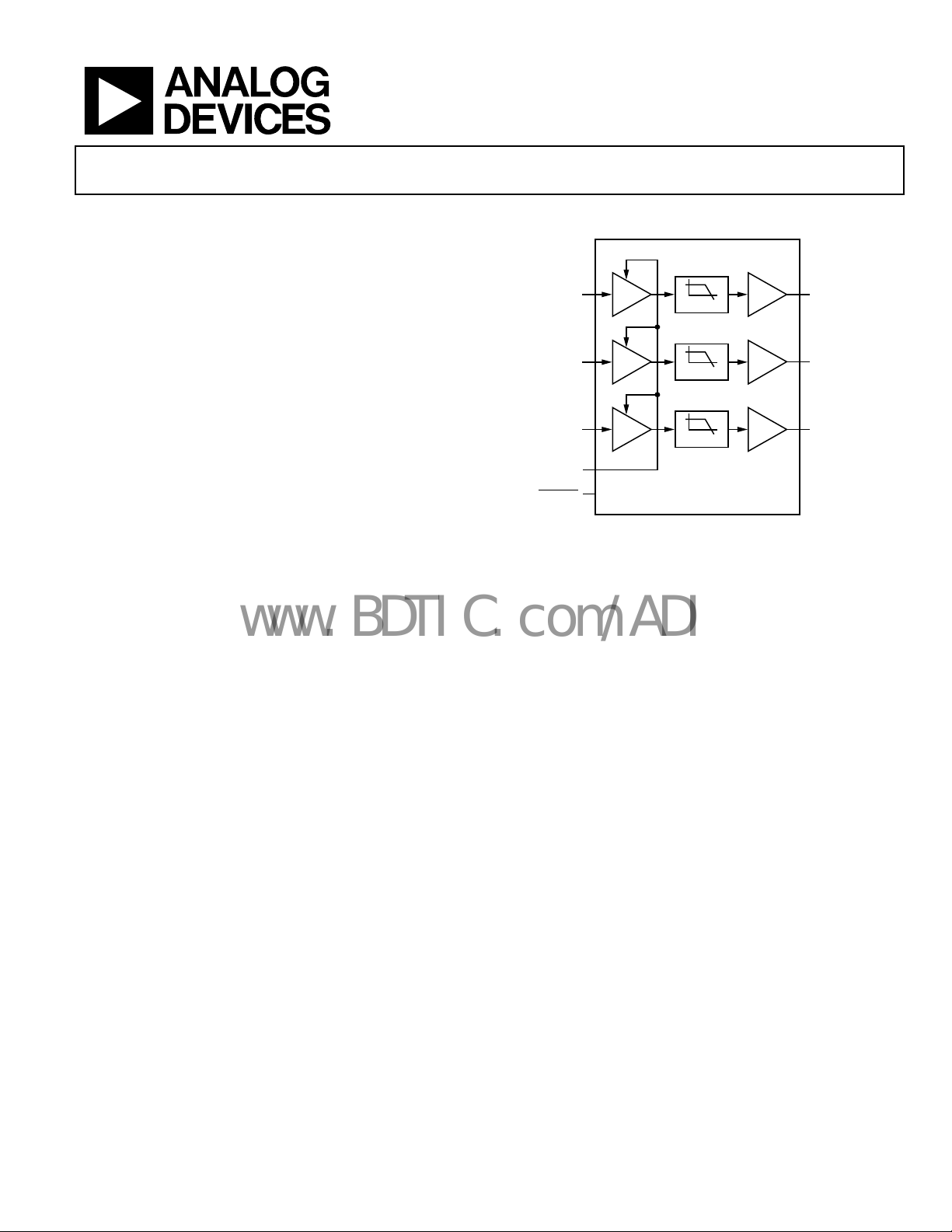
FUNCTIONAL BLOCK DIAGRAM
Y/G IN
Pb/B IN
Pr/R IN
DCO
DISABLE
×1
×1
×1
36MHz
36MHz
36MHz
ADA4417-3
Figure 1.
×2
×2
×2
Y/G OUT
Pb/B OUT
Pr/R OUT
06221-001
The ADA4417-3 is a low cost, fully integrated, video
reconstruction filter specifically designed for consumer high
definition video. With 1 dB frequency flatness out to 38 MHz,
and 44 dB of rejection at 75 MHz, the ADA4417-3 can handle
the most demanding HD video applications.
The ADA4417-3 operates on a single 3.3 V to 5 V supply. It is
ell-suited for applications where power consumption is
w
critical. A disable feature allows for further power conservation
by reducing the supply current to 10 µA (typical) when the
device is not in use. With rail-to-rail output, it can be efficiently
used on a 3.3 V supply, while providing the user with a 2 V p-p
output. The buffers can drive two 75 Ω terminated loads, either
dc- or ac-coupled.
Rev. 0
Information furnished by Analog Devices is believed to be accurate and reliable. However, no
responsibility is assumed by Anal og Devices for its use, nor for any infringements of patents or ot her
rights of third parties that may result from its use. Specifications subject to change without notice. No
license is granted by implication or otherwise under any patent or patent rights of Analog Devices.
Trademarks and registered trademarks are the property of their respective owners.
The ADA4417-3 also has an output dc offset function that can
o
perate in two states. When the DCO pin is tied to V
video signal at the output is offset by 200 mV. When the DCO
pin is tied to ground, the output dc level follows the input level.
The ADA4417-3 is available in a 10-lead MSOP package and is
ra
ted for operation over the extended industrial temperature
range of −40°C to +85°C.
One Technology Way, P.O. Box 9106, Norwood, MA 02062-9106, U.S.A.
Tel: 781.329.4700 www.analog.com
Fax: 781.461.3113 ©2006 Analog Devices, Inc. All rights reserved.
CC
, the

ADA4417-3
www.BDTIC.com/ADI
TABLE OF CONTENTS
Features .............................................................................................. 1
Theory of Operation ...................................................................... 12
Applications....................................................................................... 1
Functional Block Diagram .............................................................. 1
General Description......................................................................... 1
Revision History ............................................................................... 2
Specifications..................................................................................... 3
Absolute Maximum Ratings............................................................ 5
Thermal Resistance ...................................................................... 5
ESD Caution.................................................................................. 5
Pin Configuration and Function Descriptions............................. 6
Typical Performance Characteristics ............................................. 7
Test Cir c ui t ...................................................................................... 11
REVISION HISTORY
7/06—Revision 0: Initial Version
Applications..................................................................................... 13
Overview ..................................................................................... 13
Disable ......................................................................................... 13
Output DC Offset Control........................................................ 13
Input and Output Coupling ...................................................... 13
Printed Circuit Board Layout ................................................... 13
Video Encoder Reconstruction Filter...................................... 14
Outline Dimensions ....................................................................... 15
Ordering Guide .......................................................................... 15
Rev. 0 | Page 2 of 16
ADA4417-3
www.BDTIC.com/ADI
SPECIFICATIONS
VS = 5 V (@ TA = 25°C, VIN = 1 V p-p, G = +2, RT = 0 Ω1, RL = 150 Ω, DCO = 1, unless otherwise noted).
Table 1.
Parameter Test Conditions/Comments Min Typ Max Unit
OVERALL PERFORMANCE
DC Offset DCO = 1, input referred 70 100 142 mV
DCO = 0, input referred 40 mV
Input Voltage Range See Note 2
Output Voltage Range 0.08 4.73 V
Linear Output Current Per channel 30 mA
DC Voltage Gain 5.88 6.07 dB
Integrated Voltage Noise f = 100 kHz to 30 MHz, input referred 0.4 mV rms
Filter Input Bias Current 3.2 μA
Slew Rate 150 V/μs
Settling Time to 0.5% 65 ns
Output Overdrive Recovery 125 ns
Total Harmonic Distortion f = 1 MHz, VIN = 0.7 V p-p 0.01 %
Gain Matching 0.01 0.09 dB
FILTER DYNAMIC PERFORMANCE
−1 dB Bandwidth 27 38 MHz
−3 dB Bandwidth 31 42 MHz
Out-of-Band Rejection f = 75 MHz 38 44 dB
Crosstalk f = 5 MHz, input referred, RT = 275 Ω
Propagation Delay f = 5 MHz 26 ns
Group Delay Variation f = 1 MHz to 36 MHz 5 ns
Differential Gain Modulated 10 step ramp, sync tip at 0 V 0.06 %
Differential Phase Modulated 10 step ramp, sync tip at 0 V 0.21 Degrees
DISABLE PERFORMANCE
DISABLE Assert Voltage
DISABLE Assert Time
DISABLE Deassert Voltage
DISABLE Deassert Time
DISABLE Input Bias Current
Input-to-Output Isolation—Disabled
POWER SUPPLY
Operating Range 3.3 to 5.0 V
Quiescent Current DCO = 0 19.5 22.5 mA
DCO = 1 24.0 29.5 mA
Quiescent Current—Disabled
PSRR DCO = 0 55 71 dB
1
See Figure 25.
2
Limited by output range.
0.8 V
100 ns
2.0 V
2.0 μs
32 μA
f = 5 MHz, DISABLE
DCO = 0, DISABLE
= 0
= 0
1
−68 dB
92 dB
10 μA
2
Rev. 0 | Page 3 of 16

ADA4417-3
www.BDTIC.com/ADI
VS = 3.3 V (@ TA = 25°C, VIN = 1.0 V p-p, G = +2, RT = 0 Ω1, RL = 150 Ω, DCO = 1, unless otherwise noted).
Table 2.
Parameter Test Conditions/Comments Min Typ Max Unit
OVERALL PERFORMANCE
DC Offset DCO = 1, input referred 66 100 145 mV
DCO = 0, input referred 42 mV
Input Voltage Range See Note 2
Output Voltage Range 0.08 3.05 V
Linear Output Current Per channel 20 mA
DC Voltage Gain 5.75 6.16 dB
Integrated Voltage Noise f = 100 kHz to 30 MHz, input referred 0.4 mV rms
Filter Input Bias Current 3.2 μA
Slew Rate 130 V/μs
Settling Time to 0.5% 70 ns
Output Overdrive Recovery 125 ns
Total Harmonic Distortion f = 1 MHz, VIN = 0.7 V p-p 0.08 %
Gain Matching 0.02 0.18 dB
FILTER DYNAMIC PERFORMANCE
−1 dB Bandwidth 27 38 MHz
−3 dB Bandwidth 31 42 MHz
Out-of-Band Rejection f = 75 MHz 40 44 dB
Crosstalk f = 5 MHz, input referred, RT = 275 Ω
Propagation Delay f = 5 MHz 26.5 ns
Group Delay Variation f = 1 MHz to 36 MHz 4 ns
Differential Gain Modulated 10 step ramp, sync tip at 0 V 0.07 %
Differential Phase Modulated 10 step ramp, sync tip at 0 V 0.14 Degrees
DISABLE PERFORMANCE
DISABLE Assert Voltage
DISABLE Assert Time
DISABLE Deassert Voltage
DISABLE Deassert Time
DISABLE Input Bias Current
Input-to-Output Isolation—Disabled
POWER SUPPLY
Operating Range 3.3 to 5.0 V
Quiescent Current DCO = 0 19.0 21.5 mA
DCO = 1 22.5 29.0 mA
Quiescent Current—Disabled
PSRR DCO = 0 52 71 dB
1
See Figure 25.
2
Limited by output range.
0.8 V
110 ns
2.0 V
3.0 μs
19 μA
f = 5 MHz, DISABLE
DCO = 0, DISABLE
= 0
= 0
1
−61 dB
92 dB
10 μA
2
Rev. 0 | Page 4 of 16
ADA4417-3
www.BDTIC.com/ADI
ABSOLUTE MAXIMUM RATINGS
Table 3.
Parameter Rating
Supply Voltage 5.5 V
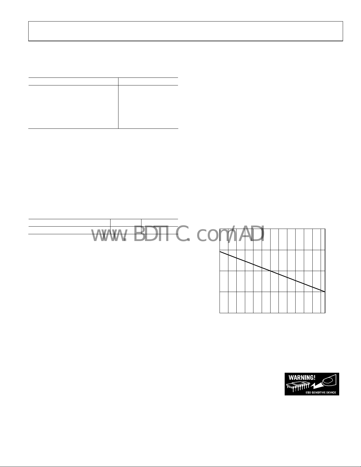
Power Dissipation See Figure 2
Storage Temperature Range −65°C to +125°C
The power dissipated in the package (P
quiescent power dissipation and the power dissipated in the
package due to the load drive for all outputs. The quiescent
power is the supply voltage (V
Assuming the load (R
Operating Temperature Range −40°C to +85°C
Lead Temperature (Soldering 10 sec) 300°C
Junction Temperature 150°C
Stresses above those listed under Absolute Maximum Ratings
may cause permanent damage to the device. This is a stress
rating only; functional operation of the device at these or any
other conditions above those indicated in the operational
section of this specification is not implied. Exposure to absolute
maximum rating conditions for extended periods may affect
device reliability.
THERMAL RESISTANCE
θJA is specified for the worst-case conditions, that is, a device
soldered in a circuit board for surface-mount packages.
Table 4.
Package Type θ
JA
Unit
some of which is dissipated in the package and some in the load
(V
RMS output voltages should be considered. If R
GND, the total power is V
Airflow increases heat dissipation, effectively reducing θ
addition, more metal directly in contact with the package leads
from metal traces, through holes, ground, and power planes
reduce the θ
Figure 2 shows the maximum safe power dissipation in the
p
(130°C/W) on a JEDEC standard 4-layer board. θ
approximate.
10-Lead MSOP 130 °C/W
Maximum Power Dissipation
The maximum safe power dissipation in the ADA4417-3
package is limited by the associated rise in junction temperature
(T
) on the die. At approximately 150°C, which is the glass
J
transition temperature, the plastic changes its properties. Even
temporarily exceeding this temperature limit can change the
stresses that the package exerts on the die, permanently shifting
the parametric performance of the ADA4417-3. Exceeding a
junction temperature of 175°C for an extended period can
result in changes in the silicon devices potentially causing
failure.
) times the quiescent current (IS).
S
) is midsupply, then the total drive power is
L
/2 × I
V
S
OUT
× I
OUT
).
JA
× I
S
OUT
.
OUT
ackage vs. the ambient temperature for the 10-lead MSOP
2.0
1.5
1.0
0.5
MAXIMUM POWER DISSIPATION (W)
0
–40 –30 –20 –10 0 10 20 30 40 50 60 70 80
Figure 2. Maximum Power Dissipation vs. Temperature for a 4-Layer Board
AMBIENT TEMPERATURE (° C)
) is the sum of the
D
.
is referenced to
L
. In
JA
values are
JA
06221-002
ESD CAUTION
ESD (electrostatic discharge) sensitive device. Electrostatic charges as high as 4000 V readily accumulate on
the human body and test equipment and can discharge without detection. Although this product features
proprietary ESD protection circuitry, permanent damage may occur on devices subjected to high energy
electrostatic discharges. Therefore, proper ESD precautions are recommended to avoid performance
degradation or loss of functionality.
Rev. 0 | Page 5 of 16

ADA4417-3
www.BDTIC.com/ADI
PIN CONFIGURATION AND FUNCTION DESCRIPTIONS
1
Y/G IN
DISABLE
2
ADA4417-3
3
Pb/B IN
DCO
Pr/R IN
(Not to Scale)
4
5
Figure 3. Pin Configuration
TOP VIEW
10
9
8
7
6
Y/G OUT
VCC
Pb/B OUT
GND
Pr/R OUT
06221-003
Table 5. Pin Function Descriptions
Pin No. Mnemonic Description
1 Y/G IN Y/G HD Video Input
2
DISABLE
Disable/Power Down (Active Low)
3 Pb/B IN Pb/B HD Video Input
4 DCO Output DC Offset Enable
5 Pr/R IN Pr/R HD Video Input
6 Pr/R OUT Pr/R HD Video Output
7 GND Ground
8 Pb/B OUT Pb/B HD Video Output
9 VCC Power Supply
10 Y/G OUT Y/G HD Video Output
Rev. 0 | Page 6 of 16

ADA4417-3
www.BDTIC.com/ADI
TYPICAL PERFORMANCE CHARACTERISTICS
Default Conditions: VS = 5 V, TA = 25°C, VO = 2 V p-p, G = +2, RT = 0 Ω (see Figure 25), RL = 150 Ω, DCO = 1, unless otherwise noted.
9
6
3
BLACK LINE: VS = 3.3V
0
GRAY LINE: V
–3
–6
–9
–12
–15
–18
–21
–24
GAIN (dB)
–27
–30
–33
–36
–39
–42
–45
–48
1 10 100 500
= 5V
S
FREQUENCY (M Hz)
Figure 4. Frequency Response vs. Supply
9
6
3
BLACK LINE: RL = 75Ω
0
GRAY LINE: R
–3
–6
–9
–12
–15
–18
–21
–24
GAIN (dB)
–27
–30
–33
–36
–39
–42
–45
–48
1 10 100 500
= 150Ω
L
FREQUENCY (M Hz)
Figure 5. Frequency Response vs. Load
9
6
3
0
–3
–6
–9
–12
–15
–18
–21
–24
GAIN (dB)
–27
–30
–33
–36
–39
–42
–45
–48
1 10 100 500
FREQUENCY (M Hz)
Figure 6. Frequency Response vs. Temperature
–40°C (5V)
+25°C (5V)
+85°C (5V)
06221-004
06221-005
06221-006
7.0
BLACK LINE: VS = 3.3V
GRAY LINE: V
6.5
6.0
5.5
5.0
GAIN (dB)
4.5
4.0
3.5
3.0
110
= 5V
S
FREQUENCY (MHz )
Figure 7. Flatness Response vs. Supply
7.0
BLACK LINE: RL = 75Ω
GRAY LINE: R
6.5
6.0
5.5
5.0
GAIN (dB)
4.5
4.0
3.5
3.0
110
= 150Ω
L
FREQUENCY (MHz )
Figure 8. Flatness Response vs. Load
7.0
6.5
6.0
5.5
5.0
GAIN (dB)
4.5
4.0
3.5
3.0
–40°C (5V)
+25°C (5V)
+85°C (5V)
110
FREQUENCY (MHz )
Figure 9. Flatness Response vs. Temperature
100
06221-007
100
06221-008
100
06221-009
Rev. 0 | Page 7 of 16

ADA4417-3
–
–
www.BDTIC.com/ADI
9
6
3
BLACK LINE: VS = 0.2V p-p
0
GRAY LINE: V
–3
–6
–9
–12
–15
–18
–21
–24
GAIN (dB)
–27
–30
–33
–36
–39
–42
–45
–48
1 10 100 500
= 2.0V p-p
S
FREQUENCY (M Hz)
Figure 10. Frequency Response vs. Amplitude
10
REFERRED TO INPUT
0
–10
–20
–30
–40
PSRR (dB)
–50
–60
–70
–80
0.01 1010.1 100 500
FREQUENCY (M Hz)
VS = 3.3V, DCO = H
VS = 3.3V, DCO = L
VS = 5V, DCO = H
VS = 5V, DCO = L
Figure 11. PSRR vs. Frequency
20
VIN = 1V p-p
DISABLE = 0
–30
–40
–50
–60
–70
–80
OFF ISOLATION (dB)
–90
–100
–110
–120
1 10 100 500
FREQUENCY (M Hz)
Figure 12. Off Isolation vs. Fr
BLACK LINE: VS = 3.3V
GRAY LINE: V
equency
S
= 5V
06221-010
06221-011
06221-012
36
BLACK LINE: VS = 3.3V
GRAY LINE: V
34
32
30
28
GROUP DELAY (ns)
26
24
110
= 5V
S
FREQUENCY (MHz )
Figure 13. Group Delay vs. Frequency
10k
DISABLE = 0
1k
IMPEDANCE (Ω)
100
0.1 1 10010 500
Figure 14. Output Impedance (D
FREQUENCY (M Hz)
isabled) vs. Frequency
30
REFERRED TO INPUT
R
= 275Ω
T
–40
–50
–60
–70
CROSSTALK (dB)
–80
–90
–100
0.1 1 10010 500
FREQUENCY (M Hz)
BLACK LINE: VS = 3.3V
GRAY LINE: V
Figure 15. Crosstalk vs. Frequency
100
06221-013
06221-014
= 5V
S
06221-015
Rev. 0 | Page 8 of 16

ADA4417-3
www.BDTIC.com/ADI
OUTPUT AMPL ITUDE (V)
BLACK LINE: VS = 3.3V
250mV/DIV 50ns/DIV
GRAY LINE: V
S
= 5V
4.00
3.75
3.50
3.25
3.00
2.75
2.50
2.25
VOLTAGE (V)
2.00
1.75
1.50
06221-016
1.25
1.00
OUTPUT
1.0%, 61ns
0.5%, 63ns
2 × INPUT
ERROR
50ns/DIV
0.5%/DIV
06221-019
Figure 16. Transient Response
5.5
5.0
4.5
4.0
3.5
3.0
2.5
2.0
VOLTAGE (V)
1.5
1.0
0.5
0
–0.5
DISABLE INPUT
OUTPUT
1µs/DIV
06221-017
5.5
5.0
4.5
4.0
3.5
3.0
2.5
2.0
VOLTAGE (V)
1.5
1.0
0.5
0
–0.5
Figure 17. Enable Turn On Time
6
5
4
3
2
VOLTAGE (V)
1
0
–1
OUTPUT (DCO = 0)
Figure 18. Output Ove
2 × INPUT
OUTPUT (DCO = 1)
rdrive Recovery
100ns/DIV
06221-018
300
VS = 5V
275
+ (mV)
S
250
225
200
OUTPUT VOLTAGE WRT V
175
150
–40 80655035205–10–25
Figure 21. Output Saturation Voltage vs. Temperature
Figure 19. Settling Time
DISABLE INPUT
OUTPUT
Figure 20. Enable Turn Off Time
TEMPERATURE (°C)
1µs/DIV
06221-020
06221-021
Rev. 0 | Page 9 of 16

ADA4417-3
www.BDTIC.com/ADI
30
BLACK LINE: VS = 3.3V
GRAY LINE: V
27
24
21
SUPPLY CURRENT (mA)
18
S
= 5V
DCO = 1
DCO = 0
30
25
20
15
10
POWER SUPPLY CURRENT (mA)
5
VS = 5V,
DISABLE AND DCO
TIED TOGETHER,
= OPEN
R
L
= +85°C
T
A
= +25°C
T
A
= –40°C
T
A
15
–40 80706050403020100–10–20–30
5.0
4.5
4.0
3.5
3.0
2.5
2.0
1.5
OUTPUT VOLTAGE (V)
1.0
0.5
0
–0.25 2.752.251.751.250.750.25
TEMPERATURE (°C)
Figure 22. Supply Current vs. Temperature
DCO = 1
DCO = 0
INPUT VOLTAGE (V)
Figure 23. Output Voltage vs. Input Voltage
0
0 0.2 0.4 0.6 0.8 1.0 1.2 1.4 1.6 1.8 2.0
06221-022
Figure 24. Supply Current vs.
DISABLE AND DCO VOL TAGE (V)
DISABLE
/DCO Voltage and Temperature
06221-024
06221-023
Rev. 0 | Page 10 of 16

ADA4417-3
www.BDTIC.com/ADI
TEST CIRCUIT
NETWORK
ANALYZER Tx
50Ω
R
= 150Ω
L
R
T
DUT
50Ω 86.6Ω
118Ω
NETWORK
ANALYZER Rx
50Ω
MINIMUM-L OSS MATCHI NG NETW ORK LOSS CAL IBRATED OUT
Figure 25. Basic Test Circuit for Swept Frequency Measurements
06221-025
Rev. 0 | Page 11 of 16

ADA4417-3
www.BDTIC.com/ADI
THEORY OF OPERATION
The ADA4417-3 is a low cost, integrated video filtering and
driving solution that offers a 38 MHz, 1 dB bandwidth to meet
the requirements of high definition video. Each of the three
filters has a sixth-order Butterworth response that includes
group delay equalization. Group delay variation from 1 MHz to
36 MHz is only 5 ns, resulting in greater stop-band attenuation
and minimal phase distortion.
The ADA4417-3 is designed to operate in many video
vironments. With a supply range of 3.3 V to 5 V, it requires
en
a relatively low nominal quiescent current of 10 mA per
channel. This makes the ADA4417-3 well suited for portable
high definition video applications. Additionally, for other low
power applications, the part can be powered down to draw
typically 10 µA by pulling the
ADA4417-3 is also well suited for high encoding frequency
applications because it maintains a stop-band attenuation of over
40 dB out to 500 MHz. Typical power supply rejection ratio
(PSRR) is greater than 70 dB, providing excellent rejection in
systems with supplies that are noisy or underregulated.
DISABLE
pin to ground. The
The ADA4417-3 is intended to accept dc-coupled inputs
f
rom an encoder or other ground-referenced video signals.
The ADA4417-3 inputs are high impedance. No minimum or
maximum input termination is required; however, terminations
above 1 kΩ may degrade crosstalk performance at high
frequencies.
Each filter input includes level-shifting circuitry. The level-
hifting circuitry adds a dc component of 100 mV to ground-
s
referenced input signals so that they reproduce accurately,
without the output buffers hitting the ground rail. For lowest
off state power consumption when using the dc offset function,
it is recommended that the DCO and
together.
The output drivers on the ADA4417-3 have rail-to-rail output
pabilities with 6 dB gain. Each output is capable of driving
ca
two ac- or dc-coupled, 75 Ω source-terminated loads. If a large
dc output level is required while driving two loads, ac coupling
should be used to limit the power dissipation.
DISABLE
pins be tied
Rev. 0 | Page 12 of 16

ADA4417-3
A
Ω
www.BDTIC.com/ADI
APPLICATIONS
OVERVIEW
With its high impedance inputs and high output drive, the
ADA4417-3 is ideally suited to video reconstruction and
antialias filtering applications. The high impedance inputs give
designers flexibility with regard to how the input signals are
terminated. Devices with DAC current source outputs that feed
the ADA4417-3 can be loaded in whatever resistance provides
the best performance, and devices with voltage outputs can be
optimally terminated as well. The ADA4417-3 outputs can each
drive up to two source-terminated, 75 Ω loads and can
therefore directly drive the outputs from set-top boxes, DVDs,
and a like without the need for a separate output buffer.
DISABLE
The ADA4417-3 includes a disable feature that can be used to
save power when a particular device is not in use. The disable
feature is asserted by pulling the
DISABLE
pin to ground.
Tabl e 6 summarizes the disable feature operation.
Table 6.
DISABLE
V
S
DISABLE
Pin Connection Status
Function
Enabled
GND Disabled
OUTPUT DC OFFSET CONTROL
The ADA4417-3 has a fixed, pin-selectable, input-referred dc
offset. When the DCO pin is tied to V
, the output is offset by
S
200 mV, preventing the video sync tips from hitting the ground
rail. When DCO is tied to GND, the dc level of the output
follows that of the input.
Tabl e 7 summarizes the dc offset operation.
Table 7. DC Offset Function
DCO Pin Connection Status
V
S
Output offset = 200 mV
GND No output offset
INPUT AND OUTPUT COUPLING
Inputs to the ADA4417-3 may be ac- or dc-coupled. AC
coupling requires suitable circuitry following the ac coupling
element to provide proper dc level and bias currents at the input
stages. The ADA4417-3 outputs can be either ac- or dc-coupled.
When driving single, ac-coupled loads in standard 75 Ω video
dist
ribution systems, 220 µF coupling capacitors are recommended
for use on all but the chrominance (Y) signal output. Because
the chrominance signal is a narrow-band modulated carrier, it
has no low frequency content and can therefore be coupled with
a 0.1 µF capacitor.
Rev. 0 | Page 13 of 16
There are two ac coupling options when driving two loads from
o
ne output. One simply uses the same value capacitor on the
second load, while the other is to use a common coupling
capacitor that is at least twice the value used for the single load
(see
Figure 26 and Figure 27).
When driving two parallel 150 Ω loads (75 Ω effective load), the
andwidth of the filters typically varies from that of the
3 dB b
filters with a single 150 Ω load. Typical variation is within ±2.5%.
75Ω
CABLE
220µF
470µF
75Ω
75Ω
75Ω
CABLE
220µF
75Ω
75Ω
75
CABLE
75Ω
75Ω
CABLE
75Ω
ds with One Common Coupling Capacitor
75Ω
75Ω
06221-027
06221-026
ADA4417-3
Figure 26. Driving Two AC-Coupled Loads with Two Coupling Capacitors
DA4417-3
Figure 27. Driving Two AC-Coupled Loa
PRINTED CIRCUIT BOARD LAYOUT
As with all high speed applications, attention to printed circuit
board layout is of paramount importance. Standard high speed
layout practices should be adhered to when designing with the
ADA4417-3. A solid ground plane is recommended, and
surface-mount, ceramic power supply decoupling capacitors
should be placed as close as possible to the supply pins. All of
the ADA4417-3 GND pins should be connected to the ground
plane with traces that are as short as possible. Controlled
impedance traces of the shortest length possible should be used
to connect to the signal I/O pins and should not pass over any
voids in the ground plane. A 75 Ω impedance level is typically
used in video applications. All signal outputs of the ADA4417-3
should include series termination resistors when driving
transmission lines.
When the ADA4417-3 receives its inputs from a device with
urrent outputs, the required load resistor value for the output
c
current is often different from the characteristic impedance of
the signal traces. In this case, if the interconnections are sufficiently
short (<< 0.1 wavelength), the trace does not have to be
terminated in its characteristic impedance. Traces of 75
can be used in this instance, provided their lengths are an inch
or two at most. This is easily achieved because the ADA4417-3
and the device feeding it are usually adjacent to each other, and
connections can be made that are less than one inch in length.

ADA4417-3
V
www.BDTIC.com/ADI
DCO
0.1µF
5
(ANALOG)
7
VCC
VIDEO ENCODER RECONSTRUCTION FILTER
The ADA4417-3 is easily applied as a reconstruction filter at the
DAC outputs of a video encoder. Figure 28 illustrates how to use
e ADA4417-3 in this type of application with an ADV7322 video
th
encoder in a single-supply application with ac-coupled outputs.
DC OFFSET
CONTROL
4
VIDEO ENCO DER
VIDEO
DAC
OUTPUTS
ADV7322
DISABLE/POWER
DOWN CONTRO L
R
L
R
L
R
L
2
DISABLE
1
Y/G IN
3
Pb/B IN
5
Pr/R IN
ADA4417-3
GND
11
Y/G OUT
Pb/B OUT
Pr/R OUT
0.1µF (Y)/
220µF (G)
75Ω
10
220µF
75Ω
8
220µF
75Ω
6
6221-028
Figure 28. The ADA4417-3 Applied as a Video Reconstruction Filter Following the ADV7322
Rev. 0 | Page 14 of 16

ADA4417-3
www.BDTIC.com/ADI
OUTLINE DIMENSIONS
3.10
3.00
2.90
6
10
3.10
3.00
2.90
1
PIN 1
0.50 BSC
0.95
0.85
0.75
0.15
0.05
0.33
0.17
COPLANARITY
0.10
COMPLIANT TO JEDEC STANDARDS MO-187-BA
Figure 29. 10-Lead Mini Small Outline Package [MSOP]
5.15
4.90
4.65
5
1.10 MAX
SEATING
PLANE
0.23
0.08
8°
0°
(RM-10)
Dimensions shown in millimeters
0.80
0.60
0.40
ORDERING GUIDE
Model Temperature Range Package Description Package Option Order Quantity Branding
ADA4417-3ARMZ
ADA4417-3ARMZ-R7
ADA4417-3ARMZ-RL
1
Z = Pb-free part.
1
−40°C to +85°C 10-Lead MSOP RM-10 1 H0Q
1
−40°C to +85°C 10-Lead MSOP RM-10 1,000 H0Q
1
−40°C to +85°C 10-Lead MSOP RM-10 2,500 H0Q
Rev. 0 | Page 15 of 16

ADA4417-3
www.BDTIC.com/ADI
NOTES
©2006 Analog Devices, Inc. All rights reserved. Trademarks and
registered trademarks are the property of their respective owners.
D06221-0-7/06(0)
Rev. 0 | Page 16 of 16
 Loading...