

Page 1
Low Distortion, DOCSIS 3.0, Upstream CATV
FEATURES
Supports CableLabs® DOCSIS 3.0/2.0 and EuroDOCSIS
3.0/2.0 specifications for customer premises equipment
(CPE) upstream transmission
5 V single-supply operation
Excellent adjacent channel rejection performance
−66 dBc ACPR for a single QPSK channel
−63 dBc ACPR for 4× QAM64 channels
Gain programmable in 1 dB steps over a 59 dB range
Gain range: −27 dB to +32 dB
Current-scaled output stage
Low between-burst output noise level
−70 dB mV in 160 kHz bandwidth
Maintains constant output impedance in enable, disable,
and sleep conditions
Selectable low power modes
12 mA in Tx disable
12 μA in sleep mode (full power-down)
3-wire, SPI-compatible interface
4 mm × 5 mm 24-lead LFCSP, RoHS compliant
VIN–
VIN+
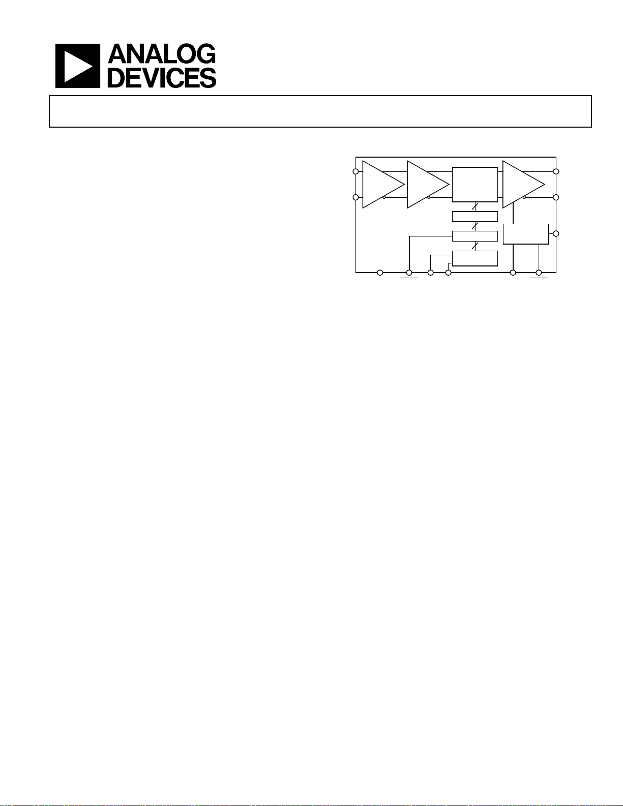
FUNCTIONAL BLOCK DIAGRAM
DIFF O R
SINGLE
INPUT
AMP
(SINGLE) = 320Ω
Z
IN
(DIFF) = 640Ω
Z
IN
ADA4320-1
VERNIER
DATEN TXEN SLEEP
ATTENUATI ON
DATA LATCH
REGISTER
CLKSDATAGND
Figure 1.
CORE
8
DECODE
8
8
SHIFT
Line Driver
ADA4320-1
POWER
AMP
Z
DIFF =
OUT
300Ω
POWER-DO WN
LOGIC
VOUT+
VOUT–
RAMP
08707-001
APPLICATIONS
DOCSIS 3.0 and EuroDOCSIS cable modems/E-MTAs
DOCSIS 3.0 set-top boxes
CATV telephony modems
Coaxial or twisted pair line drivers
GENERAL DESCRIPTION
The ADA4320-1 is a high power, ultralow distortion amplifier
designed for CATV reverse channel line driving. Its features and
specifications make the ADA4320-1 ideally suited for DOCSIS 3.0and EuroDOCSIS 3.0-based applications. Both gain and output
stage current are controlled via a 3-wire (SPI-compatible) interface.
A single 8-bit serial word selects one of four available supply
current presets and one of sixty gain codes.
The ADA4320-1 has been tailored to address both the high output
drive and stringent fidelity requirements of DOCSIS 3.0. The
part is able to maintain excellent adjacent channel rejection
performance over the full 5 MHz to 85 MHz range, even with
multiple bonded channels at maximum specified output levels.
The ADA4320-1 accepts a differential or single-ended input
signal. The output is specified for driving a single-ended 75 Ω
load through a 4:1 impedance transformer.
The ADA4320-1 features an output driver stage that scales
quiescent current consumption according to gain setting. In
multichannel mode at maximum gain (32 dB), the device draws
260 mA from a single 5 V supply, enabling the high power,
ultralow distortion performance required by multiple DOCSIS 3.0
upstream channels. For lifeline E-MTA applications, the ADA4320-1
output stage current can be throttled via SPI commands, reducing
the power requirement for single-channel transmission by up to
30%. In transmit-disable mode, the ADA4320-1 draws only 12 mA.
The device also features a full power-down sleep mode that
further reduces current draw to12 µA typical.
The ADA4320-1 is packaged in a RoHS-compliant, 24-lead
exposed pad LFCSP and is rated for operation over the −40°C
to +85°C temperature range.
Rev. A
Information furnished by Analog Devices is believed to be accurate and reliable. However, no
responsibility is assumed by Analog Devices for its use, nor for any infringements of patents or other
rights of third parties that may result from its use. Specifications subject to change without notice. No
license is granted by implication or otherwise under any patent or patent rights of Analog Devices.
Trademarks and registered trademarks are the property of their respective owners.
One Technology Way, P.O. Box 9106, Norwood, MA 02062-9106, U.S.A.
Tel: 781.329.4700 www.analog.com
Fax: 781.461.3113 ©2010 Analog Devices, Inc. All rights reserved.
Page 2

ADA4320-1
TABLE OF CONTENTS
Features .............................................................................................. 1
General Applications ................................................................. 11
Applications ....................................................................................... 1
Functional Block Diagram .............................................................. 1
General Description ......................................................................... 1
Revision History ............................................................................... 2
Specifications ..................................................................................... 3
Logic Inputs (TTL-/CMOS-Compatible Logic) ....................... 4
Timing Requirements .................................................................. 5
Absolute Maximum Ratings ............................................................ 6
Thermal Resistance ...................................................................... 6
Maximum Power Dissipation ..................................................... 6
ESD Caution .................................................................................. 6
Pin Configuration and Function Descriptions ............................. 7
Typical Performance Characteristics ............................................. 8
Applications Information .............................................................. 11
Circuit Description .................................................................... 11
Programming .............................................................................. 11
Current Level and Gain Adjustment ....................................... 11
Power Saving Features ............................................................... 12
Input Bias, Impedance, and Termination ................................ 12
Output Bias, Impedance, and Termination ............................ 12
Power Supply ............................................................................... 12
Signal Integrity Layout Considerations ................................... 12
Initial Power-Up ......................................................................... 12
RAMP Pin Feature ..................................................................... 13
Output Transformer ................................................................... 13
Outline Dimensions ....................................................................... 14
Ordering Guide .......................................................................... 14
REVISION HISTORY
10/10—Rev. 0 to Rev. A
Changes to Product Title ................................................................. 1
Changes to Pin 14, Description, Table 6 ........................................ 7
Changes to Current Level and Gain Adjustment Section ......... 11
Changes to Output Bias, Impedance, and
Termination Section ....................................................................... 12
Changes to Figure 24 ...................................................................... 13
Changes to Ordering Guide .......................................................... 14
4/10—Revision 0: Initial Version
Rev. A | Page 2 of 16
Page 3

ADA4320-1
SPECIFICATIONS
TA = 25°C, VS = 5 V, RL = 75 Ω, VIN (differential) = 29 dB mV sinusoidal, f = 5 MHz to 85 MHz, gain, V
output of Coilcraft PWB-4-BL transformer, unless otherwise noted.
Table 1.
Parameter Conditions Min Typ Max Unit
INPUT CHARACTERISTICS
Input Resistance Balanced (differential) input 640 Ω
Unbalanced (single-ended) input 320 Ω
Input Capacitance 2.0 pF
GAIN CONTROL Current Level 3
Gain Range 57.5 59 60 dB
Maximum Gain Gain Code 60 30.5 32 dB
Minimum Gain Gain Code 01 −27 −25.5 dB
Output Step Size 0.6 1.0 1.4 dB/LSB
OUTPUT CHARACTERISTICS
Gain Flatness Referenced to 10 MHz
At Maximum Gain f = 42 MHz, Gain Code 60, Current Level 3 −0.3 dB
f = 65 MHz, Gain Code 60, Current Level 3 −0.7 dB
f = 85 MHz, Gain Code 60, Current Level 3 −1.1 dB
At Minimum Gain f = 42 MHz, Gain Code 01, Current Level 0 −0.4 dB
f = 65 MHz, Gain Code 01, Current Level 0 −0.8 dB
f = 85 MHz, Gain Code 01, Current Level 0 −1.8 dB
1 dB Compression Point (P
Output Noise in 160 kHz Bandwidth f = 10 MHz, 294 Ω resistor across VIN+ and VIN− pins
At Maximum Gain Gain Code 60, Current Level 3, TXEN = high (1) −19 −20 dB mV
Gain Code 60, Current Level 0, TXEN = high (1) −20 −21 dB mV
At Minimum Gain Gain Code 01, Current Level 3, TXEN = high (1) −59 −60 dB mV
Gain Code 01, Current Level 0, TXEN = high (1) −60 −61 dB mV
Transmit Disabled TXEN = low (0) −68 −70 dB mV
Output Impedance (Measured at
Transformer Output)
Output Return Loss (Measured at
Transformer Output)
OVERALL PERFORMANCE
Adjacent Channel Power Ratio (ACPR)
Single QPSK Channel
4x QAM64 Channels
Output Third-Order Intercept Point (OIP3) f1 = 84 MHz, f2 = 85 MHz, Gain Code 60, Current Level 3 93 dB mV
f
Input-to-Output Isolation f = 85 MHz, Gain Code 60, TXEN = Low (0) 107 dB
) f = 10 MHz, Gain Code 60, Current Level 3, output referred 70 dB mV
1dB
TXEN = high (1) or TXEN = low (0) or SLEEP = low (0)
f = 85 MHz
= high (1), TXEN = high (1)
SLEEP
= high (1), TXEN = low (0)
SLEEP
= low (0)
SLEEP
f = 5 MHz to 85 MHz, output level = 61 dB mV,
Gain Code 60, Current Level 3, channel width = 6.4 MHz,
adjacent channel width = 6.4 MHz
f = 5 MHz to 85 MHz, output level = 53 dB mV/channel,
Gain Code 60, Current Level 3, channel width = 1.6 MHz,
adjacent channel width = 1.6 MHz
= 84 MHz, f2 = 85 MHz, Gain Code 60, Current Level 0 87 dB mV
1
(single-ended) measured at
OUT
75 Ω
12 dB
11 dB
10 dB
−66 dBc
−63 dBc
Rev. A | Page 3 of 16
Page 4

ADA4320-1
Parameter Conditions Min Typ Max Unit
POWER CONTROL
Transmit Enable Settling Time TXEN = 0 to 1, Gain Code 60, no input signal 5.5 µs
Transmit Disable Settling Time TXEN = 1 to 0, Gain Code 60, no input signal 7 µs
Output Switching Transients Gain Code 60 20 mV p-p
Gain Code 01 2 mV p-p
POWER SUPPLY
Operating Range 4.75 5.00 5.25 V
Quiescent Current
At Maximum Gain Gain Code 60, Current Level 3 260 300 mA
Gain Code 60, Current Level 2 235 270 mA
Gain Code 60, Current Level 1 210 250 mA
Gain Code 60, Current Level 0 180 210 mA
At Minimum Gain Gain Code 01, Current Level 3 77 100 mA
Gain Code 01, Current Level 2 73 95 mA
Gain Code 01, Current Level 1 70 90 mA
Gain Code 01, Current Level 0 65 80 mA
TXEN = 0, all gain codes, all current levels 12 15 mA
OPERATING TEMPERATURE RANGE −40 +85 °C
= 0 (power-down)
SLEEP
12 80 µA
LOGIC INPUTS (TTL-/CMOS-COMPATIBLE LOGIC)
DATEN
, CLK, SDATA, TXEN,
Table 2.
Parameter Min Typ Max Unit
Logic 1 Voltage 2.0 VS V
Logic 0 Voltage 0 0.8 V
Digital Input Leakage Current (Both Logic Levels, All Digital Pins) −5 +5 µA
SLEEP
, VS = 5 V; full temperature range.
Rev. A | Page 4 of 16
Page 5
ADA4320-1
A
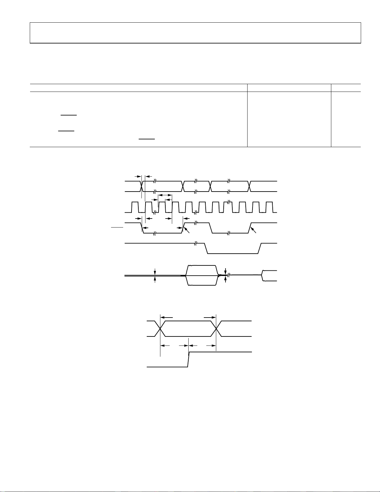
TIMING REQUIREMENTS
Full temperature range, VCC = 5 V, tR = tF = 4 ns, f
Table 3.
Parameter Min Typ Max Unit
Clock Pulse Width (tWH) 16 ns
Clock Period (tC) 32 ns
Setup Time SDATA vs. Clock (tDS) 5 ns
Setup Time DATEN vs. Clock (tES)
Hold Time SDATA vs. Clock (tDH) 5 ns
Hold Time DATEN vs. Clock (tEH)
Input 10% to 90% Rise and Fall Times, SDATA, DATEN, Clock
t
DS
SDATA
CLK
DATEN
= 8 MHz, unless otherwise noted.
CLK
VALID DATA- WORD G 1
MSB...LSB
t
C
t
WH
t
ES
8 CLOCK CYCLES
t
EH
GAIN TRANSFER (G1) GAIN TRANSFER (G2)
VALID DATA-WORD G2
16 ns
3 ns
10 ns
TXEN
NALOG
OUTPUT
SIGNAL AMPL ITUDE (p-p)
08707-002
Figure 2. Serial Interface Timing
VALID DATA BIT
SDATA MSB MSB – 1 MSB – 2
CLK
t
DS
Figure 3. SDATA Timing
t
DH
08707-003
Rev. A | Page 5 of 16
Page 6

ADA4320-1
ABSOLUTE MAXIMUM RATINGS
Table 4.
Parameter Rating
Supply Voltage 5.5 V
Maximum Power Dissipation 1.65 W
Storage Temperature Range −65°C to +125°C
Operating Temperature Range −40°C to +85°C
Lead Temperature (Soldering, 10 sec) 300°C
Junction Temperature 150°C
Stresses above those listed under Absolute Maximum Ratings
may cause permanent damage to the device. This is a stress
rating only; functional operation of the device at these or any
other conditions above those indicated in the operational
section of this specification is not implied. Exposure to absolute
maximum rating conditions for extended periods may affect
device reliability.
THERMAL RESISTANCE
θ
is specified for the device soldered to a high thermal
JA
conductivity 4-layer (2s2p) circuit board, as described in
EIA/JESD 51-7.
MAXIMUM POWER DISSIPATION
The maximum safe power dissipation in the ADA4320-1 package
is limited by the associated rise in junction temperature (T
) on
J
the die. At approximately 150°C, which is the glass transition
temperature, the plastic changes its properties. Even temporarily
exceeding this temperature limit can change the stresses that
the package exerts on the die, permanently shifting the parametric
performance of the ADA4320-1. Exceeding a junction temperature
of 150°C for an extended time can result in changes in the silicon
devices, potentially causing failure.
Airflow increases heat dissipation, effectively reducing θ
JA
. In
addition, more metal directly in contact with the package leads
from metal traces, through-holes, ground, and power planes,
reduces the θ
. The exposed paddle on the underside of the
JA
package must be soldered to a pad on the PCB surface that is
thermally connected to a copper plane to achieve the specified θ
.
JA
ESD CAUTION
Table 5. Thermal Resistance
Package Type θJA θ
24-lead LFCSP 31.2 5.7 °C/W
Unit
JC
Rev. A | Page 6 of 16
Page 7

ADA4320-1
+
–
PIN CONFIGURATION AND FUNCTION DESCRIPTIONS
COMP
VOUT
VOUT–VOUT+VOUT
4
3
1
GND
2
GND
3
VCC
VCC
VCC
RAMP
TXEN 13
NOTES
1. EXPOSED THERMAL PAD MUST BE ELECTRICALLY AND
THERMALLY CONNECTED TO PCB GROUND (G ND) PLANE.
ADA4320-1
4
TOP VIEW
(Not to Scale
5
6
7
82
92
10 22
GND
GND
VIN–
Figure 4. Pin Configuration, Top View
19
GND
18
GND
17
GND
16
SLEEP
15
CLK
14
SDATA
DATEN
11 21
12
GND 20
VIN+
08707-005
Table 6. Pin Function Descriptions
Pin No. Mnemonic Description
1, 2, 8, 9, 12,
GND Common External Ground Reference.
17, 18, 19,
EPAD
3, 4, 5 VCC Common Positive External Supply Voltage.
6 RAMP External RAMP Capacitor (Optional).
7 TXEN Transmit Enable. Logic 0 disables forward transmission, and Logic 1 enables forward transmission.
10 VIN− Inverting Input. DC-biased to approximately VCC/2. This pin should be ac-coupled with a 0.1 µF capacitor.
11 VIN+ Noninverting Input. DC-biased to approximately VCC/2. This pin should be ac-coupled with a 0.1 µF capacitor.
13
DATEN
Data Enable Low Input. This port controls the 8-bit parallel data latch and shift register. A Logic 0-to-1 transition
transfers the latched data to the attenuator core (updates the gain) and simultaneously inhibits serial data transfer
into the register. A 1-to-0 transition inhibits the data latch (holds the previous, and simultaneously enables the
register for serial data load).
14 SDATA
Serial Data Input. This digital input allows an 8-bit serial control word to be loaded into the internal register with the
most significant bit (MSB) first to adjust both the gain and current levels.
15 CLK
Clock Input. The clock port controls the serial attenuator data transfer rate to the 8-bit master-slave shift register. A
Logic 0-to-1 transition latches the data bit, and a Logic 1-to-0 transition transfers the data bit to the slave. This
requires the input serial data-word to be valid at or before this clock transition.
16
SLEEP
Low Power Sleep Mode. In sleep mode, the supply current is reduced to 12 µA typical. Logic 0 powers down
the device, and Logic 1 powers up the device.
20, 22 VOUT− Negative Output Signal. This pin must be biased to VCC.
21, 23 VOUT+ Positive Output Signal. This pin must be biased to VCC.
24 COMP Internal Compensation. This pin must be externally decoupled (0.1 F capacitor).
Rev. A | Page 7 of 16
Page 8

ADA4320-1
TYPICAL PERFORMANCE CHARACTERISTICS
TA = 25°C, VS = 5 V, RL = 75 Ω, VIN (differential) = 29 dBmV sinusoidal, f = 5 MHz to 85 MHz, Gain Code 60 (maximum), Current Level 3
(maximum), V
300
250
200
150
SUPPLY CURRENT (mA)
100
(single-ended) measured at output of Coilcraft PWB-4-BL transformer, unless otherwise noted.
OUT
CURRENT LEVEL 3
CURRENT LEVEL 2
CURRENT LEVEL 1
CURRENT LEVEL 0
VIN = 29dBmV
60
45
30
15
0
GAIN (dB)
–15
–30
–45
CURRENT LEVEL 3
V
= 29dBmV
IN
GAIN CODE 60
GAIN CODE 40
GAIN CODE 20
GAIN CODE 01
50
0 6 12 18 24 30 36 42 48 54 60
GAIN CODE
Figure 5. Supply Current vs. Gain Code
275
GAIN CODE 60
CURRENT LEVEL 3
270
265
260
255
250
SUPPLY CURRENT (mA)
245
240
235
–60 –40 –20 0 20 40 60 80 100
AMBIENT TEMPERATURE (°C)
5.25V
5.00V
4.75V
Figure 6. Supply Current vs. Ambient Temperature at Maximum Gain
75
GAIN CODE 01
CURRENT LEVEL 0
70
5.25V
65
60
SUPPLY CURRENT (mA)
55
5.00V
4.75V
–60
1M 1G100M10M
08707-006
FREQUENCY (Hz)
08707-009
Figure 8. Gain vs. Frequency
1.0
CURRENT LEVEL 3
CURRENT LEVEL 2
CURRENT LEVEL 1
0.5
CURRENT LEVEL 0
0
–0.5
–1.0
NORMALIZE D GAIN (dB)
–1.5
–2.0
58807570656055504540353025201510
08707-007
FREQUENCY (MHz)
GAIN CODE 60 (MAXIMUM)
V
= 29dBmV
IN
5
08707-010
Figure 9. Normalized Frequency Response at Maximum Gain
1.0
+85°C
+25°C
0.5
–40°C
0
–0.5
–1.0
–1.5
NORMALIZE D GAIN (dB)
–2.0
–2.5
GAIN CODE 60 (MAXIMUM)
V
= 29dBmV
IN
50
–60 –40 –20 0 20 40 60 80 100
AMBIENT TEMPERATURE (°C)
Figure 7. Supply Current vs. Ambient Temperature at Minimum Gain
08707-008
Rev. A | Page 8 of 16
–3.0
58807570656055504540353025201510
FREQUENCY (MHz)
Figure 10. Normalized Frequency Response over Temperature
5
08707-011
Page 9

ADA4320-1
–
–
–
–
–20
10
TXEN = 1, AL L CURRENT L EVELS
TXEN = 0
80
70
CURRENT LEVEL 3
CURRENT LEVEL 0
–30
–40
–50
–60
–70
NOISE PO WER IN 160kHz BANDWIDTH (d BmV)
–80
06054484236302418126
GAIN CODE
Figure 11. Noise Power vs. Gain Code
0
SLEEP
TX DISABLE
TX ENABLE
–5
–10
–15
–20
OUTPUT RET URN LOSS (d B)
–25
–30
585807570656055504540353025201510
FREQUENCY (MHz )
Figure 12. Output Return Loss (S22) vs. Frequency
61
SINGLE QPSK CHANNEL
OUTPUT LEVEL = 61dBmV
GAIN CO DE 60 (MAXIMUM)
–62
CHANNEL WIDTH = 6.4MHz
ADJACENT CHANNEL WIDTH = 6.4MHz
–63
–64
–65
CURRENT LEVEL 0
CURRENT LEVEL 1
CURRENT LEVEL 2
CURRENT LEVEL 3
60
50
40
30
OUTPUT 1d B COMPRESSI ON POINT (dBmV)
20
0654484236302418126
08707-013
GAIN CODE
0
08707-014
Figure 14. Output 1 dB Compression Point vs. Gain Code
40
–45
–50
–55
–60
–65
–70
–75
ADJACENT CHANNEL POW ER RATIO (d Bc)
–80
08707-012
SINGLE Q PSK CHANNEL
INPUT LEVEL = 29dBmV
CURRENT LEVEL 3
CHANNEL WIDT H = 6.4MHz
DRIVEN CHANNEL CENTER = 42MHz
ADJACENT CHANNEL WI DTH = 6.4MHz
ADJACENT CHANNEL CENTER = 48.4MHz
ACPR
OUTPUT
LEVEL
0654484236302418126
GAIN CODE
80
70
60
50
40
30
OUTPUT LEVEL (dBmV)
20
10
0
0
08707-017
Figure 15. ACPR and Output Level vs. Gain Code
52
4× QAM64 CHANNELS (UNCORRELATED)
OUTPUT LE VEL = 53dBmV/CHANNEL
GAIN CODE 60 (MAXIMUM)
–54
CHANNEL WIDTH = 1.6MHz
ADJACENT CHANNEL WI DTH = 1.6MHz
–56
CURRENT LEVEL 0
–58
–60
CURRENT LEVEL 1
CURRENT LEVEL 2
CURRENT LEVEL 3
–66
–67
ADJACENT CHANNEL POW ER RATIO (d Bc)
–68
58575655545352515
FREQUENCY (MHz )
Figure 13. ACPR vs. Frequency for Single QPSK Channel
08707-015
–62
–64
ADJACENT CHANNEL POW ER RATIO (d Bc)
–66
5875655545352515
FREQUENCY (MHz )
Figure 16. ACPR vs. Frequency for 4× QAM64 Channels
5
08707-016
Rev. A | Page 9 of 16
Page 10

ADA4320-1
–24
SINGLE Q PSK CHANNEL
GAIN CODE 42 ( 14dB)
–28
CHANNEL WIDTH = 6.4MHz
DRIVEN CHANNEL CENTE R = 42 MHz
–32
ADJACENT CHANNEL WI DTH = 6.4 MHz
ADJACENT CHANNEL CENTER = 48.4 MHz
ADJACENT CHANNEL POW ER RATIO (dBc)
–36
–40
–44
–48
–52
–56
–60
–64
–68
–72
CURRENT LEVEL 0
CURRENT LEVEL 1
CURRENT LEVEL 2
CURRENT LEVEL 3
25 4241403938373635343332313029282726
INPUT LEVEL (dBmV)
Figure 17. ACPR vs. Input Level for a Single QPSK Channel
–10
SINGLE Q PSK CHANNEL
GAIN CODE 60 (MAXIMUM)
CHANNEL WIDT H = 6.4 MHz
DRIVEN CHANNEL CE NTER = 42M Hz
–20
ADJACENT CHANNEL WI DTH = 6.4MHz
ADJACENT CHANNEL CENT ER = 48. 4MHz
–30
–40
CURRENT LEVEL 0
CURRENT LEVEL 1
CURRENT LEVEL 2
CURRENT LEVEL 3
08707-018
–22
4× QAM 64 CHANNELS ( UNCORRELATE D)
GAIN CODE 42 ( 14dB)
CHANNEL WIDT H = 1.6 MHz
–28
DRIVEN CHANNEL CE NTER = 77. 8MHz, 79.4M Hz,
81.0MHz, 82.6MHz
ADJACENT CHANNEL WI DTH = 1.6MHz
ADJACENT CHANNEL CENT ER = 84. 2MHz
–34
CURRENT LEVEL 0
CURRENT LEVEL 1
–40
CURRENT LEVEL 2
CURRENT LEVEL 3
–46
–52
–58
–64
ADJACENT CHANNEL POW ER RATIO (dBc)
–70
12 3129 3028272625242322212019181716151413
INPUT LEVEL (dBmV/CHANNEL)
Figure 20. ACPR vs. Input Level for 4× QAM64 Channels
–10
4× QAM 64 CHANNELS ( UNCORRELATE D)
GAIN CODE 60 (MAXIMUM)
CHANNEL WIDT H = 1.6 MHz
DRIVEN CHANNEL CE NTER = 77. 8MHz, 79.4M Hz,
–20
81.0MHz, 82.6MHz
ADJACENT CHANNEL WI DTH = 1.6MHz
ADJACENT CHANNEL CENT ER = 84. 2MHz
–30
CURRENT LEVEL 0
CURRENT LEVEL 1
CURRENT LEVEL 2
–40
CURRENT LEVEL 3
08707-019
–50
–60
–70
ADJACENT CHANNEL POW ER RATIO (dBc)
–80
59 717069686766656463626160
OUTPUT LEVEL (dBmV)
Figure 18. ACPR vs. Output Level for a Single QPSK Channel
OUTPUT AMPL ITUDE (V)
8
6
4
2
0
–2
–4
–6
–8
–2 1814 16121086420
4× QAM 64 CHANNELS ( UNCORRELATE D)
OUTPUT LEVE L = 53dBm V/CHANNEL
CHANNEL WIDT H = 1.6 MHz
CHANNEL CENTERS = 39.6MHz, 41.2MHz, 42.8MHz, 44.4M Hz)
TXEN
PEAK OUTPUT
ENVELOPE
TIME (µs)
Figure 19. Transmit Enable/Disable Response
–50
–60
–70
ADJACENT CHANNEL POW ER RATIO (dBc)
–80
44 626058565452504846
08707-020
OUTPUT LEVEL (dBmV/CHANNEL )
08707-021
Figure 21. ACPR vs. Output Level for 4x QAM64 Channels
120
100
OUTPUT GLITCH AMPLITUDE (mV p-p)
08707-022
TXEN = 1
TXEN = 0
DOCSIS 3.0 LIMIT (FOR 29d BmV INPUT)
80
60
40
20
0
0648 544236302418126
GAIN CODE
0
08707-023
Figure 22. Output Glitch Amplitude vs. Gain Code
Rev. A | Page 10 of 16
Page 11

ADA4320-1
APPLICATIONS INFORMATION
GENERAL APPLICATIONS
The ADA4320-1 is primarily intended for use as the reverse
channel power amplifier (PA) in DOCSIS® 3.0 customer premises
equipment (CPE), including cable modems, E-MTAs, and
DOCSIS-enabled set-top boxes. The signals are typically QPSK or
QAM waveforms generated by the upstream modulator and DAC.
To sufficiently attenuate DAC images, a low-pass reconstruction
filter is recommended between the DAC output and the
ADA4320-1. A differential filter is preferred, and its output
impedance should match the 640 Ω input impedance of the
ADA4320-1.
Varying distances between the CPE and the cable modem
termination system (CMTS), as well as diplexers and splitters
that may exist in the signal path, require the amplifier to
provide a wide range of output power. The combination of a
high output level, excellent linearity, and 59 dB gain range of the
ADA4320-1 enables the CPE to overcome inline losses and
ensures adequate signal strength at the upstream termination.
CIRCUIT DESCRIPTION
In power-up mode, the ADA4320-1 comprises three analog
functions. The input amplifier (preamp) can be used single-ended
or balanced (differential). If the input is used in the balanced
configuration, it is imperative that the input signals be 180° out
of phase and of equal amplitude. A Vernier adjustment amplifier
controls the 1 dB gain steps.
The digital attenuator (DA) stage provides coarse adjustment in
6 dB steps. It also scales the current supplied to the output stage.
Both the preamp and DA are differential (balanced) to improve
power supply rejection and linearity.
The differential current is output from the DA to the output stage.
The output stage, with its 300 Ω balanced output impedance,
maintains proper matching to a 75 Ω load when used with a
2:1 (turns ratio) balun transformer.
PROGRAMMING
The ADA4320-1 is controlled via a unidirectional, 3-wire serial
DATEN
interface (SPI-compatible) consisting of CLK,
signals. An 8-bit data-word containing the output stage current
level (Bits[7:6]) and desired gain code (Bits[5:0]) is clocked into
the SDATA port, MSB first.
The programmable current level (CL) range of the ADA4320-1 is
CL3 (highest) to CL0 (lowest). The programmable gain range is
+32 dB (Gain Code 60) to −27 dB (Gain Code 01), in steps of 1 dB
per least significant bit (LSB), providing a total gain range of 59 dB.
, and SDATA
Table 7. Data-Word for Setting Current and Gain Levels
CL
Typ ic al
Current
(mA)
CL[7:6]
(Bin)
Gain[5:0]
(Hex)
Cain
Code
(Dec)
Typ ic al
Gain (dB)
3 260 to 77 11 3C to 01 60 to 01 +32 to −27
2 235 to 73 10 3C to 01 60 to 01 +32 to −27
1 210 to 70 01 3C to 01 60 to 01 +32 to −27
0 180 to 65 00 3C to 01 60 to 01 +32 to −27
The sequence of loading the SDATA register starts on the falling
edge of the
DATEN
pin, which activates the CLK line. Data on
the SDATA line is clocked into the serial shift register on the
rising edge of CLK, MSB first. The data-word is latched into
the attenuator core on the rising edge of
DATEN
. Serial interface
timing for the ADA4320-1 is shown in and . Figure 2 Figure 3
CURRENT LEVEL AND GAIN ADJUSTMENT
Gain adjustment and current scaling allow the PA to achieve the
high output levels and linearity required for multiple-channel
DOCSIS 3.0 compliance, while offering significantly reduced
power consumption in single-channel and lifeline battery-backup
modes of operation.
There are two methods used to adjust the supply current of the
ADA4320-1. The four curves in Figure 23 represent the supply
current vs. gain code for the different current level (CL3 to
CL0). The current levels are selectable using Bit 6 and Bit 7 of
the 8-bit control word clocked into the serial data port.
In addition to the selectable current levels, the supply current is
automatically reduced for every 6 dB reduction in gain. At
higher gain settings, this is more pronounced. At maximum
gain setting and maximum current level, a step down of 6 dB
reduces the supply current by 33%.
300
CURRENT LEVEL 3
CURRENT LEVEL 2
CURRENT LEVEL 1
CURRENT LEVEL 0
250
GAIN
200
150
SUPPLY CURRENT (mA)
100
50
0 1224364860
Figure 23. Gain and Current Scaling
GAIN CO DE
30
18
6
–6
–18
–30
GAIN (dB)
08707-024
Rev. A | Page 11 of 16
Page 12

ADA4320-1
POWER SAVING FEATURES
The ADA4320-1 incorporates three distinct methods for
reducing power consumption that include the following:
• Transmit disable for between-burst periods
• Sleep (shutdown) mode
• Output stage current scaling
OUTPUT BIAS, IMPEDANCE, AND TERMINATION
The output stage of the ADA4320-1 requires a bias of 5 V.
The 5 V power supply should be applied to the center tap of
the output transformer through a 100 nH series inductor as
shown in Figure 24. The 100 nH inductor should be placed close
to the transformer center tap to reduce parasitic capacitance on
this node and to obtain best performance.
The asynchronous TXEN pin is used to place the ADA4320-1
into between-burst mode. In this reduced current state, the
300 differential output impedance is maintained. Applying
Logic 0 to the TXEN pin deactivates the amplifier, providing
up to 95% reduction in consumed power. For 5 V operation at
maximum gain and current level, supply current is typically
reduced from 260 mA to 12 mA. In this mode of operation,
between-burst noise is minimized and over 100 dB of input to
output isolation is achieved.
Additionally, the ADA4320-1 incorporates an asynchronous
SLEEP
pin that can be used to further reduce supply current to
approximately 12 µA. Applying Logic 0 to the
the amplifier into sleep mode.
Entering/exiting sleep mode can result in a transient voltage at the
output of the amplifier. It is recommended to perform transitions
SLEEP
on the
Additional power savings are possible by optimizing the output
stage current for different operating conditions. Typically, at
lower frequencies (5 MHz to 42 MHz), the full specified output
can be maintained in CL0 (see Figure 13 and Figure 16). For lower
input levels, the same is true, as shown in Figure 17 and Figure 20.
For per-channel output levels less than 65 dBmV (QPSK) and
50 dBmV (4× QAM64), the ADA4320-1 can maintain an ACPR
of better than −60 dBc (see Figure 18 and Figure 21) at Current
Level 0 (CL0). At higher gain settings, operating in CL0 reduces
current consumption by 30%, compared to operating in CL3.
As an example, operating in CL0, the ADA4320-1 can drive a
single QPSK channel at 61 dBmV, at maximum gain, maintaining
a worst-case ACPR of −66 dBc. It does this while drawing only
180 mA from a 5 V supply.
pin with TXEN held low.
SLEEP
pin places
INPUT BIAS, IMPEDANCE, AND TERMINATION
The VIN+ and VIN− inputs have a dc bias level of VCC/2;
therefore, the input signal should be ac-coupled as seen in the
typical application circuit (see Figure 24). The differential input
impedance of the ADA4320-1 is approximately 640 Ω, and the
single-ended input is 320 . The ADA4320-1 exhibits optimum
performance when driven with a balanced (differential) signal.
The output impedance of the ADA4320-1 is 300 differential,
regardless of whether the amplifier is in transmit enable, transmit
disable, or sleep mode. This, when combined with a 4:1 impedance
transformer, provides a 75 output match and eliminates the
need for external back termination resistors. If the output signal
is being evaluated using standard 50 test equipment, a minimum
loss 75 to 50 pad should be used to provide the test circuit
with the proper impedance match.
POWER SUPPLY
The 5 V supply should be delivered to each of the VCC pins via
a low impedance power bus. The power bus should be decoupled
with a 10 µF tantalum capacitor located close to the ADA4320-1.
Additionally, the VCC pins require decoupling to ground with
ceramic chip capacitors located close to the pins. Pin 24 (COMP),
should also be decoupled. The ideal printed circuit board (PCB)
has a low impedance ground plane covering all unused portions
of the board, except in areas of the board where input and output
traces are in close proximity to the ADA4320-1 and the output
transformer. All device GND pins, as well as the exposed pad,
must contact the PCB ground plane to ensure proper grounding
of all internal nodes.
SIGNAL INTEGRITY LAYOUT CONSIDERATIONS
Careful attention to PCB layout details can prevent problems
due to board parasitics. Proper RF design techniques are highly
recommended. All balanced input/output traces should be kept
as short as possible. This minimizes parasitic capacitance and
inductance, which is most critical between the outputs of the
ADA4320-1 and the 4:1 output transformer. It is also recommended
that all balanced signal paths be symmetrical in length and width.
Additionally, input and output traces should be adequately spaced
to minimize coupling (crosstalk) through the board. Following
these guidelines optimizes the overall performance of the
ADA4320-1 in all applications.
INITIAL POWER-UP
When supply voltage is applied to the ADA4320-1, the gain of
the amplifier is initially undetermined. During amplifier powerup, the TXEN pin should be held low (Logic 0) to prevent forward
signal transmission. Gain must then be set to the desired level,
followed by TXEN driven high. Forward signal transmission is
enabled at the resultant gain level.
Rev. A | Page 12 of 16
Page 13

ADA4320-1
V
RAMP PIN FEATURE OUTPUT TRANSFORMER
The RAMP pin (Pin 6) can be optionally used to control the
length of the burst on and off transients. By default, leaving the
RAMP pin unconnected results in a transient that is fully compliant
with DOCSIS 3.0. Adding capacitance to the RAMP pin slows
the dissipation even more.
Characterization of the ADA4320-1 was performed using a
5
+
10µF
TRANSMIT
ENABLE/DISABLE
CONTRO L
VCC
TXEN
GND
GND
VIN–
VIN+
GND
RAMP
ADA4320-1
QPSK/QAM
BURST
MODULATOR
DAC
LPF
8
0.1µF
Matching the 300 Ω differential output impedance to unbalanced
75 Ω requires a 4:1 impedance (2:1 turns) ratio transformer.
The transformer should have minimal insertion loss over the
5 MHz to 85 MHz band and have a maximum dc current rating
of at least 200 mA.
Coilcraft PWB-4-BL surface-mount wide-band RF transformer.
Alternate choices for the output transformer are the Toko
458PT-1565 and the Tyco Electronics (M/A-COM) ABACT0018.
VCC
VCC
100pF 0. 1µF
1
GND
GND
0.1µF
COMP
VOUT+
VOUT–
VOUT+
VOUT–
20
100nH
UPSTREAM
2:1*
TO TUNER
OR SPLITTER
DOWNSTREAM
DIPLEXER
F-CONNECTO R
SLEEP
*COILCRAFT PWB-4-BL
ALTERNATES : TOKO 458PT-1565
TYCO MABACT0018
8707-025
(SPI-COMPATIBLE)
3-WIRE
CONTRO L
POWER-DOWN
CONTRO L
13
GND
GND
GND
CLK
DATEN
SDATA
Figure 24. Typical Application
Rev. A | Page 13 of 16
Page 14

ADA4320-1
OUTLINE DIMENSIONS
2.75
PIN 1
INDICATOR
4.00 BSC
5.00 BSC
0.50
BSC
2.65
2.50
20
19
EXPOSED
PAD
24
1
PIN 1
INDICATOR
(Chamfer 0.225)
3.75
3.65
3.50
7
8
122409-B
SEATING
PLANE
1.00
0.90
0.80
TOP VIEW
0.30
0.25
0.20
0.05 MAX
0.02 NOM
0.20 REF
0.50
0.40
0.30
COPLANARITY
0.08
13
12
BOTTOM VIEW
FORPROPERCONNECTIONOF
THE EXPOSED PAD, REFER TO
THE PIN CONFIGURATION AND
FUNCTION DESCRIPTIONS
SECTION OF THIS DATA SHEET.
Figure 25. 24-Lead Lead Frame Chip Scale Package [LFCSP_VQ]
4 mm × 5 mm Body, Very Thin Quad
(CP-24-5)
Dimensions shown in millimeters
ORDERING GUIDE
Ordering
Model1 Temperature Range Package Description Package Option
ADA4320-1ACPZ-R7 –40°C to +85°C 24-Lead Lead Frame Chip Scale Package (LFCSP_VQ) CP-24-5 1,500
ADA4320-1ACPZ-RL –40°C to +85°C 24-Lead Lead Frame Chip Scale Package (LFCSP_VQ) CP-24-5 5,000
ADA4320-1ACPZ-EVAL Evaluation Board
1
Z = RoHS Compliant Part.
Quantity
Rev. A | Page 14 of 16
Page 15

ADA4320-1
NOTES
Rev. A | Page 15 of 16
Page 16

ADA4320-1
NOTES
©2010 Analog Devices, Inc. All rights reserved. Trademarks and
registered trademarks are the property of their respective owners.
D08707-0-10/10(A)
Rev. A | Page 16 of 16
 Loading...