1:3 and 1:4 Single-Ended, Low Cost,
V5V
V5V
FEATURES
Ideal for CATV and terrestrial applications
2.4 GHz, −3 dB bandwidth
1 dB flatness: 54 MHz to 865 MHz
Low noise figure: 4.6 dB
Low distortion
Composite second-order (CSO): −62 dBc
Composite triple beat (CTB): −72 dBc
Nominal 3 dB gain per output channel
25 dB output-to-output isolation, 50 MHz to 1000 MHz
75 Ω input and outputs
Small package size: 16-lead, 3 mm × 3 mm LFCSP
APPLICATIONS
Set-top boxes
Residential gateways
CATV distribution systems
Splitter modules
Digital cable ready (DCR) TVs
Active RF Splitters
ADA4304-3/ADA4304-4
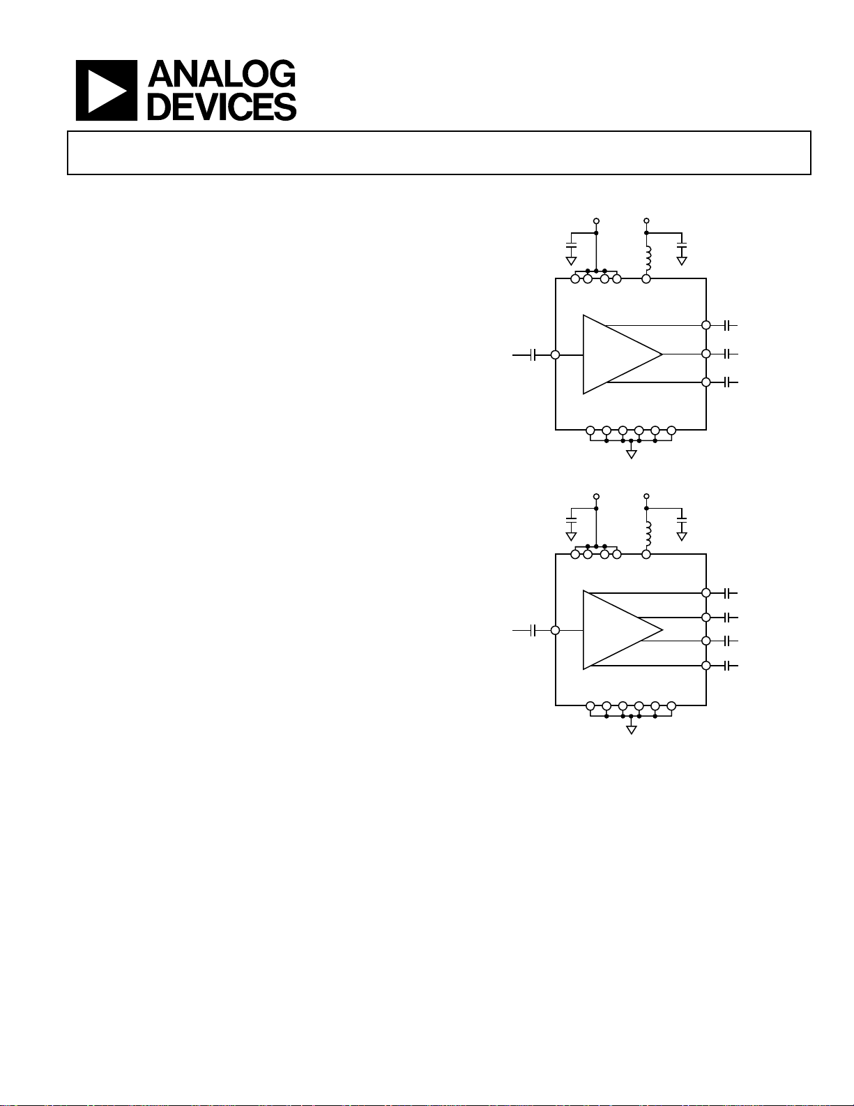
FUNCTIONAL BLOCK DIAGRAMS
5
0.1µF0.1µF
1µH
IL
GND
Figure 1.
5
1µH
VOUT1
VOUT2
VOUT3
0.01µF
0.01µF
0.01µF
0.1µF0.1µF
0.01µF
VIN
VCC
ADA4304-3
07082-001
GENERAL DESCRIPTION
The ADA4304-3/ADA4304-4 are 75 Ω active splitters for use in
applications where a lossless signal split is required. Typical
applications include multituner digital set-top boxes, cable
splitter modules, multituners/digital cable ready (DCR)
televisions, and home gateways where traditional solutions
require discrete passive splitter modules with separate fixed
gain amplifiers.
IL
GND
Figure 2.
VOUT1
VOUT2
VOUT3
VOUT4
0.01µF
0.01µF
0.01µF
0.01µF
07082-002
0.01µF
VIN
VCC
ADA4304-4
The ADA4304-3/ADA4304-4 are fabricated using the Analog
Devices, Inc., proprietary silicon germanium (SiGe),
complementary bipolar process, enabling them to achieve very
low levels of distortion with a noise figure of 4.6 dB. The parts
provide low cost alternatives that simplify designs and improve
system performance by integrating a signal splitter element and
a gain block into a single IC. The ADA4304-3/ADA4304-4 are
available in a 16-lead LFCSP and operate in the extended
industrial temperature range of −40°C to +85°C.
Rev. 0
Information furnished by Analog Devices is believed to be accurate and reliable. However, no
responsibility is assumed by Anal og Devices for its use, nor for any infringements of patents or ot her
rights of third parties that may result from its use. Specifications subject to change without notice. No
license is granted by implication or otherwise under any patent or patent rights of Analog Devices.
Trademarks and registered trademarks are the property of their respective owners.
One Technology Way, P.O. Box 9106, Norwood, MA 02062-9106, U.S.A.
Tel: 781.329.4700 www.analog.com
Fax: 781.461.3113 ©2007 Analog Devices, Inc. All rights reserved.

ADA4304-3/ADA4304-4
TABLE OF CONTENTS
Features .............................................................................................. 1
Applications....................................................................................... 1
Functional Block Diagrams............................................................. 1
General Description......................................................................... 1
Revision History ............................................................................... 2
Specifications..................................................................................... 3
Absolute Maximum Ratings............................................................ 4
Thermal Resistance ...................................................................... 4
ESD Caution.................................................................................. 4
Pin Configurations and Function Descriptions ........................... 5
REVISION HISTORY
11/07—Revision 0: Initial Version
Typical Perf or m an c e Charac t e r istics ..............................................6
Test Cir c ui t s ........................................................................................9
Applications..................................................................................... 10
Circuit Description .................................................................... 10
Evaluation Boards ...................................................................... 10
RF Layout Considerations......................................................... 10
Power Supply............................................................................... 10
Outline Dimensions ....................................................................... 12
Ordering Guide .......................................................................... 12
Rev. 0 | Page 2 of 12

ADA4304-3/ADA4304-4
SPECIFICATIONS
VCC = 5 V, 75 Ω system, TA = 25°C, unless otherwise noted.
Table 1.
ADA4304-3 ADA4304-4
Parameter Conditions Min Typ Max Min Typ Max Unit
DYNAMIC PERFORMANCE See Figure 19 for test circuit
Bandwidth (−3 dB) 2400 2400 MHz
Frequency Range 54 865 54 865 MHz
Gain f = 100 MHz 3.3 2.9 dB
Gain Flatness 54 MHz to 865 MHz 1.0 1.0 dB
NOISE/DISTORTION PERFORMANCE
Noise Figure
@ 550 MHz 4.6 4.6 dB
@ 865 MHz 4.8 4.8 dB
Output IP3 f1 = 97.25 MHz, f2 = 103.25 MHz 26 26 dBm
Output IP2 f1 = 97.25 MHz, f2 = 103.25 MHz 43 43 dBm
Composite Triple Beat (CTB) 135 channels, 15 dBmV/channel, f = 865 MHz −72 −72 dBc
Composite Second Order (CSO) 135 channels, 15 dBmV/channel, f = 865 MHz −62 −62 dBc
Cross Modulation (CXM)
INPUT CHARACTERISTICS See Figure 19 for test circuit
Input Return Loss @ 54 MHz −17 −13 −18 −14 dB
@ 550 MHz −22 −16 −21 −15 dB
@ 865 MHz −12 −8 −12 −8 dB
Output-to-Input Isolation Any output, 54 MHz to 865 MHz
@ 54 MHz −33 −30 −33 −31 dB
@ 550 MHz −33 −30 −33 −31 dB
@ 865 MHz −34 −31 −35 −32 dB
OUTPUT CHARACTERISTICS See Figure 19 and Figure 20 for test circuits
Output Return Loss Any output, 54 MHz to 865 MHz
@ 54 MHz −21 −17 −21 −17 dB
@ 550 MHz −16 −11 −17 −12 dB
@ 865 MHz −14 −9 −14 −9 dB
Output-to-Output Isolation Any output, 54 MHz to 865 MHz dB
@ 54 MHz −26 −26 dB
@ 550 MHz −25 −25 dB
@ 865 MHz −25 −25 dB
1 dB Compression (P1dB) Output referred, f = 100 MHz 9.0 8.7 dBm
POWER SUPPLY
Nominal Supply Voltage 4.75 5.0 5.25 4.75 5.0 5.25 V
Quiescent Supply Current 92 105 92 105 mA
1
Characterized with 50 Ω noise figure analyzer.
1
@ 54 MHz 4.0 4.0 dB
135 channels, 15 dBmV/channel,
100% modulation @ 15.75 kHz, f = 865 MHz
−68 −68 dBc
Rev. 0 | Page 3 of 12

ADA4304-3/ADA4304-4
ABSOLUTE MAXIMUM RATINGS
Table 2.
Parameter Rating
Supply Voltage 5.5 V
Power Dissipation See Figure 3
Storage Temperature Range −65°C to +125°C
Operating Temperature Range −40°C to +85°C
Lead Temperature (Soldering, 10 sec) 300°C
Junction Temperature 150°C
Stresses above those listed under Absolute Maximum
Ratings may cause permanent damage to the device. This is
a stress rating only; functional operation of the device at
these or any other conditions above those indicated in the
operational section of this specification is not implied.
Exposure to absolute maximum rating conditions for
extended periods may affect device reliability.
THERMAL RESISTANCE
θJA is specified for the device (including exposed pad)
soldered to a high thermal conductivity 4-layer (2s2p)
circuit board, as described in EIA/JESD 51-7.
Table 3. Thermal Resistance
Package Type θ
JA
16-Lead LFCSP (Exposed Pad) 98 °C/W
Maximum Power Dissipation
The maximum safe power dissipation in the ADA4304-3/
ADA4304-4 package is limited by the associated rise in
junction temperature (T
) on the die. At approximately
J
150°C, which is the glass transition temperature, the plastic
changes its properties. Even temporarily exceeding this
temperature limit can change the stresses that the package
exerts on the die, permanently shifting the parametric
performance. Exceeding a junction temperature of 150°C
for an extended period can result in changes in the silicon
devices, potentially causing failure.
Unit
The power dissipated in the package (P
the quiescent power dissipation, that is, the supply voltage (V
times the quiescent current (I
). In Tabl e 1, the maximum
S
power dissipation of the ADA4304-3/ADA4304-4 can be
calculated as
P
= 5.25 V × 105 mA = 551 mW
D (MAX)
Airflow increases heat dissipation, effectively reducing θ
In addition, more metal directly in contact with the package
leads/exposed pad from metal traces, through-holes, ground,
and power planes reduces the θ
JA
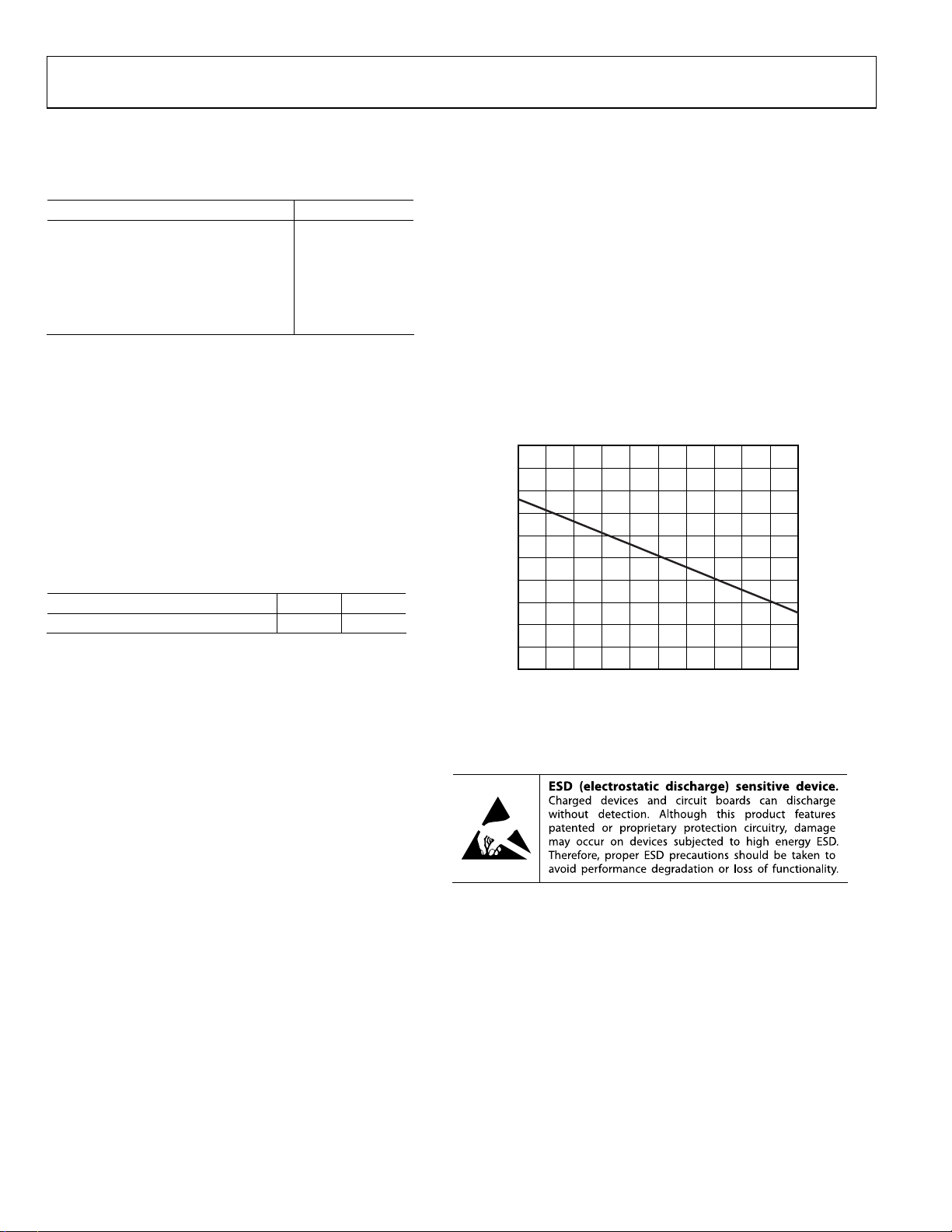
Figure 3 shows the maximum safe power dissipation in the
package vs. the ambient temperature for the 16-lead LFCSP
(98°C/W) on a JEDEC standard 4-layer board.
2.0
1.8
1.6
1.4
1.2
1.0
0.8
0.6
0.4
MAXIMUM POWER DISSIPATION (W )
0.2
0
0 100
10 20 30 40 50 60 7 0 80 90
AMBIENT TEMPERATURE (°C)
Figure 3. Maximum Power Dissipation vs. Temperature for a 4-Layer Board
ESD CAUTION
) is essentially equal to
D
.
)
S
.
JA
07082-003
Rev. 0 | Page 4 of 12

ADA4304-3/ADA4304-4
PIN CONFIGURATIONS AND FUNCTION DESCRIPTIONS
VOUT1
IL
VCC
VCC
13
14
16
15
PIN 1
INDICATOR
1VCC
ADA4304-3
2VCC
TOP VIEW
3GND
(Not to Scale)
4VIN
5
NC = NO CONNECT
GND
6
GND
12 VOUT2
11 GND
10 VOUT3
9GND
8
7
NC
GND
07082-004
Figure 4. ADA4304-3 Pin Configuration
Table 4. ADA4304-3 Pin Function Descriptions
Pin No. Mnemonic Description
1, 2, 15, 16 VCC Supply Pin.
3, 5 to 7, 9, 11 GND Ground.
4 VIN Input.
8 NC No Connection.
10 VOUT3 Output 3.
12 VOUT2 Output 2.
13 VOUT1 Output 1.
14 IL Bias Pin.
Table 5. ADA4304-4 Pin Function Descriptions
Pin No. Mnemonic Description
1, 2, 15, 16 VCC Supply Pin.
3, 5 to 7, 9, 11 GND Ground.
4 VIN Input.
8 VOUT4 Output 4.
10 VOUT3 Output 3.
12 VOUT2 Output 2.
13 VOUT1 Output 1.
14 IL Bias Pin.
CC
VCC
V
VOUT1
IL
14
13
15
16
PIN 1
1VCC
ADA4304-4
2VCC
3GND
(Not to Scale)
4VIN
INDICATOR
TOP VIEW
5
6
GND
GND
12 VOUT2
11 GN D
10 VOUT3
9GND
8
7
T4
GND
VOU
Figure 5. ADA4304-4 Pin Configuration
7082-005
Rev. 0 | Page 5 of 12

ADA4304-3/ADA4304-4
–
–
–
TYPICAL PERFORMANCE CHARACTERISTICS
VCC = 5 V, 75 Ω system, TA = 25°C, unless otherwise noted.
NOISE FI GURE (dB)
OUTPUT I P2 (dBm)
OUTPUT IP3 (dBm)
10
50Ω SYSTEM
8
6
4
2
0
60
55
50
45
40
35
30
25
20
50
40
35
30
25
20
15
10
5
0
TA = +85°C
TA = +25°C
TA = –40°C
10050
FREQUENCY (MHz )
Figure 9. Noise Figure vs. Frequency
ADA4304-3
ADA4304-4
100
FREQUE NCY (MHz)
Figure 10. Output IP2 vs. Frequency
ADA4304-3
ADA4304-4
10050
FREQUE NCY (MHz)
Figure 11. Output IP3 vs. Frequency
1000
1000
1000
07082-023
07082-010
07082-011
54
–56
–58
CSO (dBc)
–60
–62
–64
–66
–68
–70
–72
–74
TA = +25°C
TA = –40°C
10050
FREQUENCY (MHz )
TA = +85°C
Figure 6. Composite Second Order (CSO) vs. Frequency
60
–63
–66
CTB (dBc)
–69
–72
–75
–78
–81
–84
–87
–90
TA = +25°C
10050
FREQUENCY (MHz )
TA = +85°C
TA = –40°C
Figure 7. Composite Triple Beat (CTB) vs. Frequency
60
–63
–66
TA = +85°C
TA = –40°C
CXM (dBc)
–69
–72
–75
–78
–81
–84
–87
–90
TA = +25°C
10050
FREQUENCY (MHz )
Figure 8. Cross Modulation (CXM) vs. Frequency
1000
1000
1000
07082-020
07082-021
07082-022
Rev. 0 | Page 6 of 12

ADA4304-3/ADA4304-4
–
5
4
3
2
1
0
–1
GAIN (dB)
–2
–3
–4
–5
–6
100 100040
TA = +25°C
TA = +85°C
FREQUENCY (MHz )
Figure 12. ADA4304-3 Gain vs. Frequency
5
4
3
2
1
0
–1
GAIN (dB)
–2
–3
–4
–5
–6
100 100040
TA = +25°C
TA = +85°C
FREQUENCY (MHz )
Figure 13. ADA4304-4 Gain vs. Frequency
25
–27
–29
–31
–33
–35
–37
–39
–41
OUTPUT-TO-INPUT ISOLATION (dB)
–43
–45
ADA4304-3
ADA4304-4
100 100050
FREQUE NCY (MHz)
Figure 14. Output-to-Input Isolation vs. Frequency
TA = –40°C
TA = –40°C
07082-024
07082-025
07082-013
0
–5
–10
–15
–20
–25
–30
–35
OUTPUT-TO-OUTPUT ISOLATION (dB)
–40
–45
100 100050
FREQUE NCY (MHz)
Figure 15. Output-to-Output Isolation vs. Frequency
0
–5
–10
–15
–20
INPUT RETURN LOSS (dB)
–25
–30
ADA4304-4
100 100050
ADA4304-3
FREQUE NCY (MHz)
Figure 16. Input Return Loss vs. Frequency
0
–5
–10
–15
–20
OUTPUT RET URN LOSS (d B)
–25
–30
ADA4304-4
100 100050
FREQUENCY (MHz )
ADA4304-3
Figure 17. Output Return Loss vs. Frequency
ADA4304-4
ADA4304-3
07082-014
07082-015
07082-016
Rev. 0 | Page 7 of 12

ADA4304-3/ADA4304-4
100
95
90
85
80
QUIESCENT SUP PLY CURRENT (mA)
75
–60
–40
–50
–20
–30
–100102030405060708090
TEMPERATURE (°C)
Figure 18. Quiescent Supply Current vs. Temperature
100
07082-026
Rev. 0 | Page 8 of 12

ADA4304-3/ADA4304-4
TEST CIRCUITS
RF NETWORK ANAL YZER
75Ω S-PARAMETER
TEST SET
VOUTm
4
VIN
NOTES
1. TESTED FOR ALL CO MBINATIO NS OF
VOUTm AND VOUT n.
DUT
VOUTn
75Ω
07082-018
Figure 19. Test Circuit for Transmission, Isolation, and
Reflection Measurements
Figure 20. Test Circuit for Output-to-Output Isolation Measurements
RF NETWO RK ANALYZER
75Ω S-PARAMETER
TEST SET
VIN
4
75Ω
NOTES
1. TEST ED FOR ALL COMBINAT IONS O F
VOUTm AND VO UTn.
DUT
VOUTm
VOUTn
7082-019
Rev. 0 | Page 9 of 12

ADA4304-3/ADA4304-4
V
APPLICATIONS
The ADA4304-3/ADA4304-4 active splitters are primarily
intended for use in the downstream path of television set-top
boxes (STBs) that contain multiple tuners. They are typically
located directly after the diplexer in a bidirectional CATV
customer premise unit. The ADA4304-3/ADA4304-4 provide a
single-ended input and three or four single-ended outputs that
allow the delivery of the RF signal to multiple signal paths. These
paths can include, but are not limited to, a main picture tuner,
the picture-in-picture (PIP) tuner, an out-of-band (OOB) tuner,
a digital video recorder (DVR), and a cable modem (CM).
The ADA4304-3/ADA4304-4 exhibit composite second-order
(CSO) and composite triple beat (CTB) products that are −62 dBc
and −72 dBc, respectively. The use of the SiGe bipolar process
also allows the ADA4304-3/ADA4304-4 to achieve a noise figure
(NF) of 4.6 dB at 550 MHz.
CIRCUIT DESCRIPTION
The ADA4304-3/ADA4304-4 consist of a low noise buffer
amplifier followed by a resistive power divider. This arrangement
provides 3.3 dB (ADA4304-3) or 2.9 dB (ADA4304-4) of gain
relative to the RF signal present at the input of the device. The
input and each output must be properly matched to a 75 Ω
environment for distortion and noise performance to match
the data sheet specifications. AC coupling capacitors of 0.01 μF
are recommended for the input and outputs.
A 1 μH RF choke (Coilcraft chip inductor 0805LS-102X) is
required to correctly bias the internal nodes of the ADA4304-3/
ADA4304-4. It should be connected between the 5 V supply and
the IL pin (Pin 14). The choke should be placed as close as possible
to the ADA4304-3/ADA4304-4 to minimize parasitic capacitance
on the IL pin, which is critical for achieving the specified
bandwidth and flatness.
EVALUATION BOARDS
The ADA4304-3/ADA4304-4 evaluation board allows designers
to assess the performance of the parts in their particular
application. The board includes 75 Ω coaxial connectors and
75 Ω controlled-impedance signal traces that carry the input
and output signals. Power (5 V) is applied to the red VCC loop
connector, and ground is connected to the black GND loop
connector.
Figure 21 is a schematic of the evaluation board. On
the ADA4304-3 evaluation board, connector VO4 and C7 are
not populated.
RF LAYOUT CONSIDERATIONS
Appropriate impedance matching techniques are mandatory
when designing circuit boards for the ADA4304-3/ADA4304-4.
Improper characteristic impedances on traces can cause reflections
that can lead to poor linearity. The characteristic impedance of
the signal trace to the input and from each output should be
75 Ω. Any ground metal on the top surface near signal lines
should be stitched with vias to the internal ground plane, as
shown in
Figure 22. The device package exposed paddle must
be reflow soldered to a low inductance ground to achieve data
sheet performance specifications. This is achieved by connecting
the footprint ground pad with vias to a ground plane below
(see
Figure 22).
POWER SUPPLY
The 5 V supply should be applied to each VCC pin and RF
choke via a low impedance power bus. The power bus should be
decoupled to ground using a 10 μF tantalum capacitor and a 0.1
μF ceramic chip capacitor located close to the ADA4304-3/
ADA4304-4. In addition, the VCC pins should be decoupled to
ground with a 0.1 μF ceramic chip capacitor located as close to
each pin as possible.
GND
10µF
C8
0.1µF
VIN
C2
0.01μF
EXPOSED PAD
CC
+
C5
VCC
VCC
VCC
ADA4304-3/
ADA4304-4
GND
VIN
GND
Figure 21. Evaluation Board Schematic
Rev. 0 | Page 10 of 12
L1
1.0μH
IL
VCC
GND
GND
C1
0.1µF
VOUT1
VOUT2
GND
VOUT3
GND
T4
VOU
ADA4304-4 ONLY
C6
0.01μF
0.01μF
0.01μF
C7
0.01μF
VO1
C3
VO2
C4
VO3
VO4
07082-006

ADA4304-3/ADA4304-4
7082-008
Figure 22. Evaluation Board
07082-007
Figure 23. Evaluation Board Component Layout
Rev. 0 | Page 11 of 12

ADA4304-3/ADA4304-4
R
OUTLINE DIMENSIONS
0.50
0.40
PIN 1
INDICATO
1.00
0.85
0.80
SEATING
PLANE
12° MAX
3.00
BSC SQ
TOP
VIEW
0.30
0.23
0.18
*
COMPLIANT
EXCEPT FOR EXPOSED PAD DIMENSION.
2.75
BSC SQ
0.80 MAX
0.65 TYP
0.05 MAX
0.02 NOM
0.20 REF
TO
JEDEC STANDARDS MO-220-VEED-2
0.45
0.50
BSC
1.50 REF
0.60 MAX
13
12
(BOTTOM VIEW)
9
8
Figure 24. 16-Lead Lead Frame Chip Scale Package [LFCSP_VQ]
3 mm × 3 mm Body, Very Thin Quad
(CP-16-2)
Dimensions shown in millimeters
EXPOSED
PAD
0.30
16
1
4
5
PIN 1
INDICATOR
*
1.45
1.30 SQ
1.15
0.25 MIN
ORDERING GUIDE
Model Temperature Range Package Description Package Option Ordering Quantity Branding
ADA4304-3ACPZ-RL
ADA4304-3ACPZ-R7
ADA4304-3ACPZ-R2
ADA4304-4ACPZ-RL
ADA4304-4ACPZ-R7
ADA4304-4ACPZ-R2
1
Z = RoHS Compliant Part.
1
−40°C to +85°C 16-Lead LFCSP_VQ CP-16-2 5,000 H16
1
−40°C to +85°C 16-Lead LFCSP_VQ CP-16-2 1,500 H16
1
−40°C to +85°C 16-Lead LFCSP_VQ CP-16-2 250 H16
1
−40°C to +85°C 16-Lead LFCSP_VQ CP-16-2 5,000 H10
1
−40°C to +85°C 16-Lead LFCSP_VQ CP-16-2 1,500 H10
1
−40°C to +85°C 16-Lead LFCSP_VQ CP-16-2 250 H10
©2007 Analog Devices, Inc. All rights reserved. Trademarks and
registered trademarks are the property of their respective owners.
D07082-0-11/07(0)
Rev. 0 | Page 12 of 12
 Loading...