

High Performance
www.BDTIC.com/IC
FEATURES
8-bit analog-to-digital converters
140 MSPS maximum conversion rate
Low PLL clock jitter at 140 MSPS
Automatic gain matching
Automated offset adjustment
2:1 input mux
Power-down via dedicated pin or serial register
4:4:4, 4:2:2, and DDR output format modes
Variable output drive strength
Odd/even field detection
External clock input
Regenerated Hsync output
Programmable output high impedance control
Hsyncs per Vsync counter
Pb-free package
APPLICATIONS
Advanced TVs
Plasma display panels
LCDT V
HDTV
RGB graphics processing
LCD monitors and projectors
Scan converters
Pr/RED
Pr/RED
Y/GREEN
Y/GREEN
Pb/BLUE
Pb/BLUE
HSYNC1
HSYNC0
VSYNC0
VSYNC1
SOGIN1
SOGIN0
EXTCK/COAST
CLAMP
FILT
SDA
SCL
8-Bit Display Interface
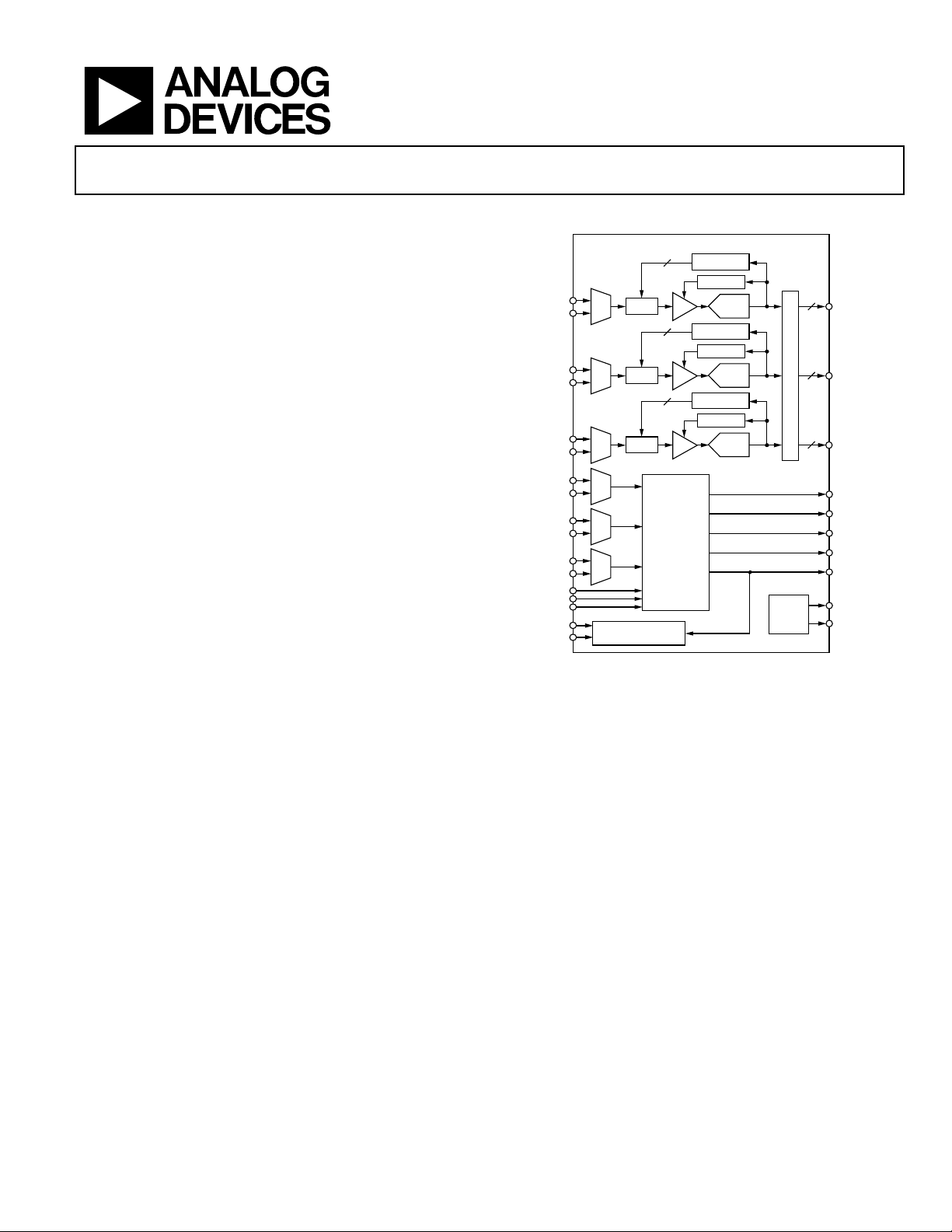
FUNCTIONAL BLOCK DIAGRAM
IN1
IN0
IN1
IN0
IN1
IN0
AD9983A
2:1
MUX
2:1
MUX
2:1
MUX
2:1
MUX
2:1
MUX
2:1
MUX
SERIAL REGI STER
CLAMP
CLAMP
CLAMP
8
PGA
8
PGA
8
PGA
SYNC
PROCESSING
PLL
POWER
MANAGEMENT
Figure 1.
AUTO OFFS ET
AUTO GAIN
8-BIT
ADC
AUTO OFFS ET
AUTO GAIN
8-BIT
ADC
AUTO OFFS ET
AUTO GAIN
8-BIT
ADC
AD9983A
8
Cb/Cr/RED
8
Y/GREEN
OUTPUT DATA F ORMATTER
8
Cb/BLUE
DATACK
SOGOUT
O/E FIELD
HSOUT
VSOUT/A0
VOLTAGE
REFS
REFHI
REFLO
OUT
OUT
OUT
06475-001
GENERAL DESCRIPTION
The AD9983A is a complete 8-bit, 140 MSPS, monolithic
analog interface optimized for capturing YPbPr video and RGB
graphics signals. Its 140 MSPS encode rate capability and full
power analog bandwidth of 300 MHz support all HDTV video
modes up to 1080i and 720p as well as graphics resolutions up
to SXGA (1280 x 1024 at 75 Hz).
The AD9983A includes a 140 MHz triple ADC with an internal
r
eference, a PLL, and programmable gain, offset, and clamp
control. The user provides only a 1.8 V power supply and an
analog input. Three-state CMOS outputs can be powered from
1.8 V to 3.3 V.
The AD9983A on-chip PLL generates a sample clock from the
ri-level sync (for YPbPr video) or the horizontal sync (for RGB
t
graphics). Sample clock output frequencies range from 10 MHz
to 140 MHz. With internal coast generation, the PLL maintains
its output frequency in the absence of sync input. A 32-step
Rev. 0
Information furnished by Analog Devices is believed to be accurate and reliable. However, no
responsibility is assumed by Anal og Devices for its use, nor for any infringements of patents or ot her
rights of third parties that may result from its use. Specifications subject to change without notice. No
license is granted by implication or otherwise under any patent or patent rights of Analog Devices.
Trademarks and registered trademarks are the property of their respective owners.
sampling clock phase adjustment is provided. Output data,
sync, and clock phase relationships are maintained.
The auto-offset feature can be enabled to automatically restore
e signal reference levels and to automatically calibrate out any
th
offset differences between the three channels. The auto channelto-channel gain matching feature can be enabled to minimize
any gain mismatches between the three channels.
The AD9983A also offers full sync processing for composite
nc and sync-on-green applications. A clamp signal is
sy
generated internally or may be provided by the user through the
CLAMP input pin.
Fabricated in an advanced CMOS process, the AD9983A is
p
rovided in a space-saving 80-lead, Pb-free, LQFP surfacemount plastic package, and is specified over the 0°C to 70°C
temperature range.
One Technology Way, P.O. Box 9106, Norwood, MA 02062-9106, U.S.A.
Tel: 781.329.4700 www.analog.com
Fax: 781.461.3113 ©2007 Analog Devices, Inc. All rights reserved.

AD9983A
www.BDTIC.com/IC
TABLE OF CONTENTS
Features.............................................................................................. 1
Applications....................................................................................... 1
Functional Block Diagram .............................................................. 1
General Description ......................................................................... 1
Revision History ............................................................................... 2
Specifications..................................................................................... 3
Analog Interface Characteristics................................................ 3
Absolute Maximum Ratings............................................................ 5
Explanation of Test Levels ........................................................... 5
Thermal Resistance ...................................................................... 5
ESD Caution.................................................................................. 5
Pin Configuration and Function Descriptions............................. 6
Theory of Operation ...................................................................... 10
Digital Inputs ..............................................................................10
Analog Input Signal Handling.................................................. 10
Hsync and Vsync Inputs............................................................ 10
Serial Control Port .....................................................................10
Output Signal Handling............................................................. 10
Clamping .....................................................................................10
Gain and Offset Control............................................................ 11
Sync-on-Green............................................................................ 12
Reference Bypassing................................................................... 12
Clock Generation ....................................................................... 13
Sync Processing........................................................................... 15
Power Management.................................................................... 18
Timing Diagrams........................................................................ 18
Hsync Timing .............................................................................19
Coast Timing............................................................................... 20
Output Formatter ....................................................................... 20
2-Wire Serial Control Port............................................................ 21
Data Transfer via Serial Interface............................................. 21
2-Wire Serial Register Map........................................................... 23
2-Wire Serial Control Registers.................................................... 29
Chip Identification..................................................................... 29
PLL Divider Control.................................................................. 29
Clock Generator Control .......................................................... 29
Phase Adjust................................................................................ 29
Input Gain................................................................................... 30
Input Offset................................................................................. 30
Hsync Controls........................................................................... 30
Vsync Controls........................................................................... 31
Coast and Clamp Controls........................................................ 32
SOG Control ............................................................................... 33
Input and Power Control........................................................... 34
Output Control........................................................................... 35
Sync Processing .......................................................................... 36
Detection Status.......................................................................... 36
Polarity Status ............................................................................. 37
Hsync Count............................................................................... 37
Test Registers............................................................................... 37
PCB Layout Recommendations.................................................... 39
Analog Interface Inputs............................................................. 39
Outputs (Both Data and Clocks).............................................. 40
Digital Inputs .............................................................................. 40
Outline Dimensions....................................................................... 41
Ordering Guide .......................................................................... 41
REVISION HISTORY
5/07—Revision 0: Initial Version
Rev. 0 | Page 2 of 44

AD9983A
www.BDTIC.com/IC
SPECIFICATIONS
ANALOG INTERFACE CHARACTERISTICS
VD = 1.8 V, VDD = 3.3 V, PVD = 1.8 V, DAVDD = 1.8 V, ADC clock = maximum conversion rate, full temperature range = 0°C to 70°C.
Table 1.
Parameter Temperature Test Level1Min Typ Max Unit
RESOLUTION
Number of bits 8 Bits
LSB Size 0.391 % of Full Scale
DC ACCURACY
Differential Nonlinearity 25°C I ±0.25 ±0.85 LSB
Full VI ±0.3 LSB
Integral Nonlinearity 25°C I ±0.75 1.45/−2.60 LSB
Full VI ±1.0 LSB
No Missing Codes Full VI GNT
ANALOG INPUT
Input Voltage Range
Minimum Full VI 0.5 V p–p
Maximum Full VI 1.0 V p–p
Gain Tempco 25°C V 125 ppm/°C
Input Bias Current 25°C
Full
Input Full-Scale Matching Full VI 1 5 % FS
Offset Adjustment Range Full VI 50 % FS
SWITCHING PERFORMANCE
Maximum Conversion Rate Full VI 140 MSPS
Minimum Conversion Rate Full IV 10 MSPS
Clock to Data Skew t
t
Full VI 4.7 μs
BUFF
t
Full VI 4.0 μs
STAH
t
Full VI 0 μs
DHO
t
Full VI 4.7 μs
DAL
t
Full VI 4.0 μs
DAH
t
Full VI 250 ns
DSU
t
Full VI 4.7 μs
STASU
t
Full VI 4.0 μs
STOSU
Maximum PLL Clock Rate Full VI 140 MHz
Minimum PLL Clock Rate Full IV 10 MHz
2
Jitter
Full IV pS p-p
Sampling Phase Tempco Full IV 15 pS/°C
DIGITAL INPUTS
Input Voltage, High (VIH) Full VI 1.0 V
Input Voltage, Low (VIL) Full VI 0.8 V
Input Current, High (IIH) Full V −1.0 μA
Input Current, Low (IIL) Full V 1.0 μA
Input Capacitance
DIGITAL OUTPUTS
Output Voltage, High (VOH) Full VI VDD − 0.1 V
Output Voltage, Low (VOL) Full VI 0.1 V
Duty Cycle, DATACK Full IV 45 50 55 %
Output Coding Binary
Full IV −0.5 2.0 ns
SKEW
25°C
25°C
IV
IV
IV pS p
V 2 pF
1
μA
1
μA
-p
Rev. 0 | Page 3 of 44

AD9983A
www.BDTIC.com/IC
Parameter Temperature Test Level1Min Typ Max Unit
POWER SUPPLY
VD Supply Voltage Full IV 1.7 1.8 1.9 V
VDD Supply Voltage Full IV 1.7 3.3 3.47 V
PVD Supply Voltage Full IV 1.7 1.8 1.9 V
DA
Supply Voltage Full IV 1.7 1.8 1.9 V
VDD
VD Supply Current (ID)
VDD Supply Current (IDD)
PVD Supply Current (IPVD)
DAVDD Supply Current (IDAVDD)
Total Power Dissipation Full VI 800 mW
Power-Down Supply Current Full VI 10 mA
Power-Down Dissipation Full VI 18 mW
DYNAMIC PERFORMANCE
Analog Bandwidth, Full Power 25°C V 300 MHz
Crosstalk Full V 60 dBc
1
See the Explanation of Test Levels section.
2
Jitter measurements taken at SXGA with recommended PLL settings.
25°C
25°C
25°C
25°C
V 250 mA
V 31 mA
V 9 mA
V 16 mA
Rev. 0 | Page 4 of 44
AD9983A
www.BDTIC.com/IC
ABSOLUTE MAXIMUM RATINGS
Table 2.
Parameter Rating
VD 1.98 V
VDD 3.6 V
PVD 1.98 V
DAVDD 1.98 V
Analog Inputs VD to 0.0 V
REFHI VD to 0.0 V
REFLO VD to 0.0 V
Digital Inputs 5 V to 0.0 V
Digital Output Current 20 mA
Operating Temperature −25°C to + 85°C
Storage Temperature −65°C to + 150°C
Maximum Junction Temperature 150°C
Maximum Case Temperature 150°C
Stresses above those listed under Absolute Maximum Ratings
y cause permanent damage to the device. This is a stress
ma
rating only; functional operation of the device at these or any
other conditions above those indicated in the operational
section of this specification is not implied. Exposure to absolute
maximum rating conditions for extended periods may affect
device reliability.
EXPLANATION OF TEST LEVELS
I. 100% production tested.
II. 100% p
III. Sample tested only.
IV. P
V. Parameter is a typical value only.
VI. 100% p
roduction tested at 25°C and sample tested at
specified temperatures.
arameter is guaranteed by design and characterization
testing.
roduction tested at 25°C; guaranteed by design and
characterization testing.
THERMAL RESISTANCE
θJA is specified for the worst-case conditions, that is, a device
soldered in a circuit board for surface-mount packages.
Table 3. Thermal Resistance
Package Type θJA θ
80-lead LQFP 35 16 °C/W
Unit
JC
ESD CAUTION
Rev. 0 | Page 5 of 44
AD9983A
V
V
V
V
T
www.BDTIC.com/IC
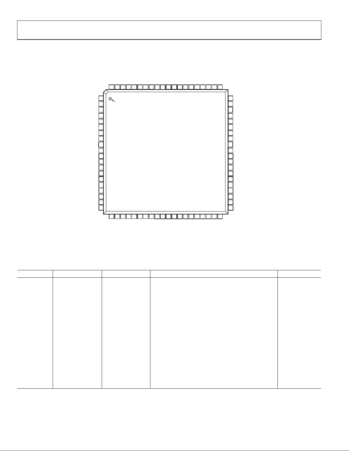
PIN CONFIGURATION AND FUNCTION DESCRIPTIONS
(1.8V)
D
B
AIN0
GND
B
AIN1
(1.8V)
D
G
AIN0
GND
SOGIN0
(1.8V)
D
G
AIN1
GND
SOGIN1
(1.8V)
D
R
AIN0
GND
R
AIN1
PWRDN
REFLO
NC
REFHI
(1.8V)
GND79PV
80
1
PIN 1
2
INDICATO R
3
4
5
6
7
8
9
10
11
12
13
14
15
16
17
18
19
20
21
22
O/E FIELD
VSOUT/A0
(1.8V)
D
FILT77GND76PV
78
23
24
HSOUT
NC = NO CONNECT
(1.8V)
D
D
GND74PV
75
25
26
27
GND
(3.3V)
DATACK
DD
SOGOUT
V
Figure 2. 80-Lead LQFP Pin
CLAMP72EXTCK/COAS
VSYNC070HSYNC069VSYNC168HSYNC167SCL66SDA65GND64V
73
71
AD9983A
TOP VIEW
(Not to Scale)
28
RED 729RED 630RED 531RED 432RED 333RED 234RED 135RED 0
Configuration
(3.3V)
DD
36NC37NC38
63NC62NC61
39
GND40GND
(3.3V)
DD
V
BLUE 0
60
BLUE 1
59
BLUE 2
58
BLUE 3
57
BLUE 4
56
BLUE 5
55
BLUE 6
54
BLUE 7
53
GND
52
VDD (3.3V)
51
NC
50
NC
49
GREEN 0
48
GREEN 1
47
GREEN 2
46
GREEN 3
45
GREEN 4
44
GREEN 5
43
GREEN 6
42
GREEN 7
41
DAVDD (1.8V)
06475-002
Table 4. Complete Pinout List
Pin Type Pin Number Mnemonic Function Value
Inputs 14 R
16 R
6 G
10 G
2 B
4 B
Channel 0 Analog Input for Converter R 0.0 V to 1.0 V
AIN0
Channel 1 Analog Input for Converter R 0.0 V to 1.0 V
AIN1
Channel 0 Analog Input for Converter G 0.0 V to 1.0 V
AIN0
Channel 1 Analog Input for Converter G 0.0 V to 1.0 V
AIN1
Channel 0 Analog Input for Converter B 0.0 V to 1.0 V
AIN0
Channel 1 Analog Input for Converter B 0.0 V to 1.0 V
AIN1
70 HSYNC0 Horizontal Sync Input for Channel 0 3.3 V CMOS
68 HSYNC1 Horizontal Sync Input for Channel 1 3.3 V CMOS
71 VSYNC0 Vertical Sync Input for Channel 0 3.3 V CMOS
69 VSYNC1 Vertical Sync Input for Channel 1 3.3 V CMOS
8 SOGIN0 Input for Sync-on-Green Channel 0 0.0 V to 1.0 V
12 SOGIN1 Input for Sync-on-Green Channel 1 0.0 V to 1.0 V
72
1
EXTCK External Clock Input 3.3 V CMOS
73 CLAMP External Clamp Input Signal 3.3 V CMOS
72
1
COAST External PLL Coast Signal Input 3.3 V CMOS
17 PWRDN Power-Down Control 3.3 V CMOS
Rev. 0 | Page 6 of 44

AD9983A
www.BDTIC.com/IC
Pin Type Pin Number Mnemonic Function Value
Outputs 28 to 35 RED [7:0] Outputs of Converter R, Bit 9 is the MSB 3.3 V CMOS
42 to 49 GREEN [7:0] Outputs of Converter G, Bit 9 is the MSB 3.3 V CMOS
54 to 61 BLUE [7:0] Outputs of Converter B, Bit 9 is the MSB 3.3 V CMOS
25 DATACK Data Output Clock 3.3 V CMOS
23 HSOUT Hsync Output Clock (Phase-Aligned with DATACK) 3.3 V CMOS
22
24 SOGOUT Sync-on-Green Slicer Output 3.3 V CMOS
21 O/E FIELD Odd/Even Field Output 3.3 V CMOS
References 78 FILT
18 REFLO Connection for External Capacitor for Input Amplifier
20 REFHI Connection for External Capacitor for Input Amplifier
Power Supply 1, 5, 9, 13 VD Analog Power Supply 1.8 V
26, 38, 52, 64 VDD Output Power Supply 1.8 V or 3.3 V
74, 76, 79 PVD PLL Power Supply 1.8 V
41 DAVDD Digital Logic Power Supply 1.8 V
Control 66 SDA Serial Port Data I/O 3.3 V CMOS
67 SCL Serial Port Data Clock (100 kHz maximum) 3.3 V CMOS
22
1
EXTCK and COAST share the same pin.
2
VSOUT and A0 share the same pin.
2
3, 7, 11, 15, 39, 40, 53,
75, 77, 80
65,
2
VSOUT Vsync Output Clock 3.3 V CMOS
Connection for External Filter Components for Internal
PLL
GND Ground 0 V
A0 Serial Port Address Input 3.3 V CMOS
Rev. 0 | Page 7 of 44

AD9983A
www.BDTIC.com/IC
Table 5. Pin Function Descriptions
Mnemonic Function Description
R
AIN0
G
AIN0
B
AIN0
R
AIN1
G
AIN1
B
AIN1
HSYNC0
HSYNC1
VSYNC0 Vertical Sync Input Channel 0
VSYNC1 Vertical Sync Input Channel 1
SOGIN0
SOGIN1
CLAMP
EXTCK/COAST External Clock
PWRDN
Analog Input for the Red
l 0
Channe
Analog Input for the Green
l 0
Channe
Analog Input for the Blue
l 0
Channe
Analog Input for the Red
l 1
Channe
Analog Input for the Green
l 1
Channe
Analog Input for the Blue
l 1
Channe
Horizontal Sync Input
l 0
Channe
Horizontal Sync Input
l 1
Channe
Sync-on-Green Input
l 0
Channe
Sync-on-Green Input
l 1
Channe
External Clamp Input
ptional)
(O
Coast Input to Clock
enerator (Optional)
G
Power-Down Control
These are high impedance inputs that accept the red, green, and blue channel graphics
, respectively. The three channels are identical and can be used for any colors,
signals
but colors are assigned for convenient reference. They accommodate input signals
ranging from 0.5 V to 1.0 V full scale. Signals should be ac-coupled to these pins to
support clamp operation. See Figure 4 and Figure 5.
These inputs receive a logic signal that establish
provides the frequency reference for pixel clock generation. The logic sense of this pin
can be automatically determined by the chip or manually controlled by Serial Register
0x12, Bits[5:4] (Hsync polarity). Only the leading edge of Hsync is used by the PLL; the
trailing edge is used in clamp timing. When Hsync polarity = 0, the falling edge of
Hsync is used. When Hsync polarity = 1, the rising edge is active. The input includes a
Schmitt trigger for noise immunity.
These are the inputs for vertical sync and provide timing information for generation of
the fiel
d (odd/even) and internal Coast generation. The logic sense of this pin can be
automatically determined by the chip or manually controlled by Serial Register 0x14,
Bits[5:4] (Vsync polarity).
These inputs process signals with embedded sync, typically on the green channel. The
pin is c
onnected to a high speed comparator with an internally generated threshold.
The threshold level can be programmed in 8 mV steps to any voltage between 8 mV
and 256 mV above the negative peak of the input signal. The default voltage threshold
is 128 mV. When connected to an ac-coupled graphics signal with embedded sync, it
produces a noninverting digital output on SOGOUT. This is usually a composite sync
signal, containing both vertical and horizontal sync information that must be separated
before passing the horizontal sync signal for Hsync processing. When not used, this
input should be left unconnected. For more details on this function and how it should
be configured, refer to the Sync-on-Green section.
This logic input can be used to define the time during which the input signal is
clamped to ground or midscale. It should be exercised when the reference dc level is
known to be present on the analog input channels, typically during the back porch of
the graphics signal. The CLAMP pin is enabled by setting the control bit clamp function
to 1, (Register 0x18, Bit 4; default is 0). When disabled, this pin is ignored and the clamp
timing is determined internally by counting a delay and duration from the trailing edge
of the Hsync input. The logic sense of this pin can be automatically determined by the
chip or controlled by clamp polarity Register 0x1B, Bits[7:6]. When not used, this pin
may be left unconnected (there is an internal pull-down resistor) and the clamp
function programmed to 0.
EXTCK allows the insertion of an external clock sour
generated, PLL locked clock. EXTCK is enabled by programming Register 0x03, Bit 2 to 1.
This pin is shared with the Coast function, which does not affect EXTCK functionality.
COAST can be used to cause the pixel clock generator to stop synchronizing with Hsync
and continue producing a clock at its current frequency and phase. This is useful when
processing signals from sources that fail to produce Hsync pulses during the vertical
interval. The coast signal is generally not required for PC-generated signals. The logic
sense of this pin can be determined automatically or controlled by Coast polarity
(Register 0x18, Bits[7:6]). When not used and EXTCK not used, this pin may be grounded
and Coast polarity programmed to 1. Input Coast polarity defaults to1 at power-up. This
pin is shared with the EXTCK function, which does not affect coast functionality. For
more details on EXTCK, see the description in this section.
This pin can be used along with Register 0x1E, Bit 3 for manual power-down control.
If manual power-down control is selected (Register 0x1E, Bit 4) and this pin is not used,
it is recommended to set the pin polarity (Register 0x1E, Bit 2) to active high and
hardwire this pin to ground with a 10 kΩ resistor.
Rev. 0 | Page 8 of 44
es the horizontal timing reference and
ce rather than the internally
AD9983A
www.BDTIC.com/IC
Mnemonic Function Description
REFLO, REFHI Input Amplifier Reference
FILT External Filter Connection
HSOUT Horizontal Sync Output
VSOUT/A0 Vertical Sync Output
Serial Port Address Input 0
SOGOUT
O/E FIELD
SDA Serial Port Data I/O Data I/O for the I2C® serial port.
SCL Serial Port Data Clock Clock for the I2C serial port.
RED [7:0] Data Output, Red Channel
GREEN [7:0] Data Output, Green Channel
BLUE [7:0] Data Output, Blue Channel
DATACK Data Clock Output
VD (1.8 V) Main Power Supply
VDD (1.8 V to 3.3 V) Digital Output Power Supply
PVD (1.8 V)
DAVDD (1.8 V) Digital Input Power Supply This supplies power to the digital logic.
GND Ground
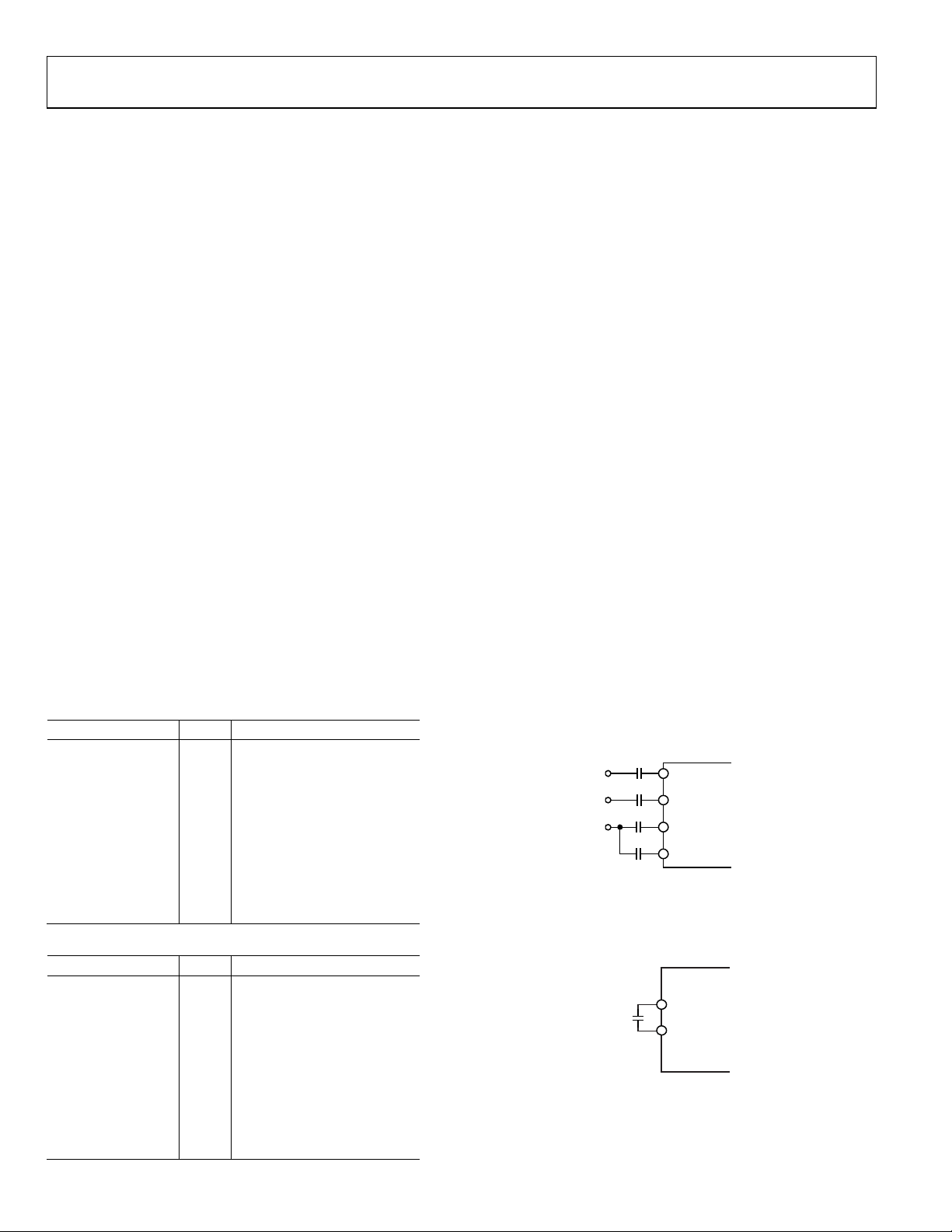
Sync-On-Green Slicer
utput
O
Odd/Even Field Bit for
terlaced Video
In
Clock Generator Power
Supply
REFLO and REFHI are connected together through a 10 μF capacitor. These are used for
y in the input ADC circuitry. See Figure 6.
stabilit
For proper operation, the pixel clock generator PLL requires an external filter. Connect the
filter sho
on th
A reconstructed and phase-aligned version of the Hsync input. Both the polarit
duration of this output can be programmed via serial bus registers. By maintaining
alignment with DATACK and Data, data timing with respect to Hsync can always be
determined.
Pin shared with A0, serial port address. This can be either a separated Vsync from a
c
be controlled via a serial bus bit. The placement and duration in all modes can be set by the
graphics transmitter or the duration can be set by Register 0x14 and Register 0x15. This pin
is shared with the A0 function, which does not affect Vsync Output functionality. For more
details on A0, see the description in the Serial Control Port section.
Pin shared with VSOUT. This pin selects the LSB of the serial port device address,
allowing t
external pull-up resistor enables this pin to be read at power-up as 1, or a high
impedance, external pull-down resistor enables this pin to be read at power-up as a 0
and not interfere with the VSOUT functionality.
This pin outputs one of four possible signals (controlled by Register 0x1D, Bits[1:0]): raw
SOG, raw Hsync, regenerated Hsync from the filter, or the filtered Hsync. See Figure 8 to
view how this pi
gets no additional processing on the AD9983A. Vsync separation is performed via the
sync separator.
This output will identify whether the current field (in an interlaced signal) is odd or even.
The main data outputs. Bit 9 is the MSB. The delay from pixel sampling time to output is
fixed. When the sampling time is changed by adjusting the phase register, the output
timing is shifted as well. The DATACK and HSOUT outputs are also moved, so the timing
relationship among the signals is maintained.
This is the main clock output signal used t
external logic. Four possible output clocks can be selected with Register 0x20, Bits[7:6].
Three of these are related to the pixel clock (pixel clock, 90° phase-shifted pixel clock
and 2× frequency pixel clock). They are produced either by the internal PLL clock
generator or EXTCK and are synchronous with the pixel sampling clock. The fourth
option for the data clock output is an internally generated 1⁄2x pixel clock.
The sampling time of the internal pixel clock can be changed by adjusting the phase
register (Register 0x04). When this is changed, the pixel related DATACK timing is also
shifted. The data, DATACK, and HSOUT outputs are all moved so that the timing
relationship among the signals is maintained.
These pins supply power to the main elements of the circuit. They should be as quiet
and
A large number of output pins (up to 29) switching at high speed (up to 140 MHz)
genera
separately from the V
transferred into the sensitive analog circuitry. If the AD9983A is interfacing with lower
voltage logic, V
compatibility.
The most sensitive portion of the AD9983A is th
provide power to the clock PLL and help the user design for optimal performance. The
designer should provide quiet, noise-free power to these pins.
The ground return for all circuitry on-chip. I
assembled on a single solid ground plane, with careful attention to ground current paths.
wn in Figure 6 to this pin. For optimal performance, minimize noise and parasitics
is node. For more information, see the PCB Layout Recommendations section.
y and
omposite signal or a direct pass through of the Vsync signal. The polarity of this output can
wo Analog Devices parts to be on the same serial bus. A high impedance
n is connected. Other than slicing off SOG, the output from this pin
o strobe the output data and HSOUT into
filtered as possible.
tes a lot of power supply transients (noise). These supply pins are identified
pins, so special care can be taken to minimize output noise
D
can be connected to a lower supply voltage (as low as 1.8 V) for
DD
e clock generation circuitry. These pins
t is recommended that the AD9983A be
Rev. 0 | Page 9 of 44

AD9983A
F
www.BDTIC.com/IC
THEORY OF OPERATION
The AD9983A is a fully integrated solution for capturing analog
RGB or YPbPr signals and digitizing them for display on
advanced TVs, flat panel monitors, projectors, and other types
of digital displays. Implemented in a high performance CMOS
process, the interface can capture signals with pixel rates of up
to 140 MHz.
The AD9983A includes all necessary input buffering, signal dc
r
estoration (clamping), offset and gain (brightness and contrast)
adjustment, pixel clock generation, sampling phase control, and
output data formatting. All controls are programmable via a
2-wire serial interface (I
analog functions makes system design straightforward and less
sensitive to the physical and electrical environment.
With a typical power dissipation of less than 800 mW and an
perating temperature range of 0°C to 70°C, the device requires
o
no special environmental considerations.
DIGITAL INPUTS
All digital inputs on the AD9983A operate to 3.3 V CMOS
levels. The following digital inputs are 5 V tolerant (that is, applying
5 V to them does not cause any damage.): HSYNC0, HSYNC1,
VSYNC0, VSYNC1, SOGIN0, SOGIN1, SDA, SCL and CLAMP.
ANALOG INPUT SIGNAL HANDLING
The AD9983A has six high impedance analog input pins for the
red, green, and blue channels. They accommodate signals
ranging from 0.5 V to 1.0 V p-p.
Signals are typically brought onto the interface board with a
VI-I connector, a 15-pin D connector, or RCA connectors.
D
The AD9983A should be located as close as possible to the
input connector. Signals should be routed using matchedimpedance traces (normally 75 Ω) to the IC input pins.
At the input pins the signal should be resistively terminated
to the signal ground return) and capacitively coupled to
(75 Ω
the AD9983A inputs through 47 nF capacitors. These capacitors
form part of the dc restoration circuit.
In an ideal world of perfectly matched impedances, the best
pe
rformance can be obtained with the widest possible signal
bandwidth. The wide bandwidth inputs of the AD9983A
(300 MHz) can track the input signal continuously as it moves
from one pixel level to the next and can digitize the pixel during
a long, flat pixel time. In many systems, however, there are
mismatches, reflections, and noise, which can result in excessive
ringing and distortion of the input waveform. This makes it
more difficult to establish a sampling phase that provides good
image quality. A small inductor in series with the input is
effective in rolling off the input bandwidth slightly and
providing a high quality signal over a wider range of conditions.
Using a Fair-Rite #2508051217Z0-High Speed, Signal Chip
Bead Inductor in the circuit shown in
esults in most applications.
r
2
C). Full integration of these sensitive
Figure 3 provides good
RGB
INPUT
Figure 3. Analog Input Interface Circuit
47n
75Ω
R
AIN
G
AIN
B
AIN
06475-003
HSYNC AND VSYNC INPUTS
The interface also accepts Hsync and Vsync signals, which are
used to generate the pixel clock, clamp timing, coast and field
information. These can be either a sync signal directly from the
graphics source, or a preprocessed TTL- or CMOS-level signal.
The Hsync input includes a Schmitt trigger buffer for immunity
o noise and signals with long rise times. In typical PC-based
t
graphic systems, the sync signals are simply TTL-level drivers
feeding unshielded wires in the monitor cable. As such, no
termination is required.
SERIAL CONTROL PORT
The serial control port is designed for 3.3 V logic; however, it is
tolerant of 5 V logic signals. Refer to the 2-Wire Serial Control
rt section.
Po
OUTPUT SIGNAL HANDLING
The digital outputs operate from 1.8 V to 3.3 V (VDD).
CLAMPING
RGB Clamping
To properly digitize the incoming signal, the dc offset of the
input must be adjusted to fit the range of the on-board ADCs.
Most graphics systems produce RGB signals with black at
g
round and white at approximately 0.75 V. However, if sync
signals are embedded in the graphics, the sync tip is often at
ground, black is at 300 mV, and white is at approximately 1.0 V.
Some common RGB line amplifier boxes use emitter-follower
buffers to split signals and increase drive capability. This
introduces a 700 mV dc offset to the signal, which must be
removed for proper capture by the AD9983A.
The key to clamping is to identify a portion (time) of the signal
w
hen the graphic system is known to be producing black. An
offset is then introduced that results in the ADC producing a
black output (Code 0x00) when the known black input is
present. The offset then remains in place when other signal
levels are processed, and the entire signal is shifted to eliminate
offset errors.
Rev. 0 | Page 10 of 44

AD9983A
www.BDTIC.com/IC
In most PC graphics systems, black is transmitted between
active video lines. With CRT displays, when the electron beam
has completed writing a horizontal line on the screen (at the
right side), the beam is deflected quickly to the left side of the
screen (called horizontal retrace) and a black signal is provided
to prevent the beam from disturbing the image.
In systems with embedded sync, a blacker-than-black signal
(H
sync) is produced briefly to signal the CRT that it is time to
begin a retrace. Because the input is not at black level at this
time, it is important to avoid clamping during Hsync. Fortunately, there is usually a period following Hsync, called the back
porch, where a good black reference is provided. This is the
time when clamping should be done.
The clamp timing can be established by simply exercising the
LAMP pin at the appropriate time with clamp source
C
(Register 0x18, Bit 4) = 1. The polarity of this signal is set by
the clamp polarity bit, (Register 0x1B, Bits[7:6]).
A simpler method of clamp timing employs the AD9983A
ternal clamp timing generator. The clamp placement register
in
(Register 0x19) is programmed with the number of pixel
periods that should pass after the trailing edge of Hsync
before clamping starts. A second register, clamp duration,
(Register 0x1A) sets the duration of the clamp. These are both
8-bit values, providing considerable flexibility in clamp
generation. The clamp timing is referenced to the trailing edge
of Hsync because, though Hsync duration can vary widely, the
back porch (black reference) always follows Hsync. A good
starting point for establishing clamping is to set the clamp
placement to 0x04 (providing 4 pixel periods for the graphics
signal to stabilize after sync) and set the clamp duration to
0x28 (giving the clamp 40 pixel periods to reestablish the
black reference).
Clamping is accomplished by placing an appropriate charge on
he external input coupling capacitor. The value of this
t
capacitor affects the performance of the clamp. If it is too small,
there will be a significant amplitude change during a horizontal
line time (between clamping intervals). If the capacitor is too
large, it will take too long for the clamp to recover from a large
change in incoming signal offset. The recommended value
(47 nF) results in recovering from a step error of 100 mV to
within 1 LSB in 30 lines with a clamp duration of 20 pixel
periods on a 85 Hz XGA signal.
YPbPr Clamping
YPbPr graphic signals are slightly different from RGB signals in
that the dc reference level (black level in RGB signals) of color
difference signals is at the midpoint of the video signal rather
than at the bottom. The three inputs are composed of
luminance (Y) and color difference (Pb and Pr) signals. For
color difference signals, it is necessary to clamp to the midscale
range of the ADC range (512) rather than to the bottom of the
ADC range (0), while the Y channel is clamped to ground.
Clamping to midscale rather than ground can be accomplished
b
y setting the clamp select bits in the serial bus register. Each of
the three converters has its own selection bit so that they can be
clamped to either midscale or ground independently. These bits
are located in Register 0x18, Bits[3:1]. The midscale reference
voltage is internally generated for each converter.
GAIN AND OFFSET CONTROL
The AD9983A contains three PGAs, one for each of the three
analog inputs. The range of the PGA is sufficient to accommodate input signals with inputs ranging from 0.5 V to 1.0 V
full scale. The gain is set in three 7-bit registers (red gain [0x05],
green gain [0x07], blue gain [0x09]). For each register, a gain
setting of 0 corresponds to the highest gain, while a gain setting
of 127 corresponds to the lowest gain. Note that increasing the
gain setting results in an image with less contrast.
The offset control shifts the analog input, resulting in a change
brightness. Three 9-bit registers red offset [Register 0x0B and
in
Register 0x0C], green offset [Register 0x0D and Register 0x0E],
and blue offset [Register 0x0F and Register 0x10] provide
independent settings for each channel. Note that the function of
the offset register depends on whether auto-offset is enabled
(Register 0x1B, Bit 5).
If manual offset is used, seven bits of the offset registers (for the
ed channel Register 0x0B, Bits[6:0]) control the absolute offset
r
added to the channel. The offset control provides ±63 LSBs of
adjustment range, with 1 LSB of offset corresponding to 1 LSB
of output code.
Automatic Offset
In addition to the manual offset adjustment mode, the
AD9983A also includes circuitry to automatically calibrate the
offset for each channel. By monitoring the output of each ADC
during the back porch of the input signals, the AD9983A can
self-adjust to eliminate any offset errors in its own ADC
channels and any offset errors present on the incoming graphics
or video signals.
To activate the auto-offset mode, set Register 0x1B, Bit 5 to 1.
N
ext, the target code registers (Register 0x0B through
Register 0x10) must be programmed. The values programmed
into the target code registers should be the output code desired
from the AD9983A ADCs, which are generated during the back
porch reference time. For example, for RGB signals, all three
registers are normally programmed to Code 2, while for YPbPr
signals the green (Y) channel is normally programmed to Code 2
and the blue and red channels (Pb and Pr) are normally set to
128. The target code registers have nine bits per channel and are
in twos complement format. This allows any value between –256
and +255 to be programmed. Although any value in this range
can be programmed, the AD9983A offset range may not be able
to reach every value. Intended target code values range from
(but are not limited to) –40 to –1 and 1 to 40 when ground
clamping and 88 to 168 when midscale clamping. Note that a
target code of 0 is not valid.
Rev. 0 | Page 11 of 44
AD9983A
www.BDTIC.com/IC
Negative target codes are included in order to duplicate a feature that is present with manual offset adjustment. The benefit
that is being mimicked is the ability to easily adjust brightness
on a display. By setting the target code to a value that does not
correspond to the ideal ADC range, the end result is an image
that is either brighter or darker. A target code higher than ideal
results in a brighter image. A target code lower than ideal
results in a darker image.
The ability to program a target code gives a large degree of
f
reedom and flexibility. In most cases all channels are set to
either 1 or 128, but the flexibility to select other values allows
for the possibility of inserting intentional skews between
channels. It also allows the ADC range to be skewed so that
voltages outside of the normal range can be digitized. For
example, setting the target code to 40 allows the sync tip, which
is normally below black level, to be digitized and evaluated.
The internal logic for the auto-offset circuit requires 16 data
cl
ock cycles to perform its function. This operation is executed
immediately after the clamping pulse. Therefore, it is important
to end the clamping pulse signal at least 16 data clock cycles
before active video. This is true whether using the AD9983A
internal clamp circuit or an external clamp signal. The autooffset function can be programmed to run continuously or on a
one-time basis (see auto-offset hold, Register 0x2C, Bit 4). In
continuous mode, the update frequency can be programmed
(Register 0x1B, Bits[4:3]). Continuous operation with updates
every 64 Hsyncs is recommended.
A guideline for basic auto-offset operation is shown in
a
nd Tabl e 7 .
Tabl e 6
Table 6. RGB Auto-Offset Register Settings
Register Value Comments
0x0B 0x02 Sets red target to 4
0x0C 0x00 Must be written
0x0D 0x02 Sets green target to 4
0x0E 0x00 Must be written
0x0F 0x02 Sets blue target to 4
0x10 0x00 Must be written
0x18, Bits[3:1] 000
0x1B, Bits[5:3] 110
Sets red, green, and blue
ls to ground clamp
channe
Selects update rate and
es auto-offset.
enabl
Table 7. PbPr Auto-Offset Register Settings
Register Value Comments
0x0B 0x40 Sets Pr (red) target to 128
0x0C 0x00 Must be written
0x0D 0x02 Sets Y (green) target to 4
0x0E 0x00 Must be written
0x0F 0x40 Sets Pb (blue) target to 128
0x10 0x00 Must be written
0x18 Bits[3:1] 101
0x1B, Bits[5:3] 110
Sets Pb, Pr to midscale clamp
Y to ground clamp
and
Selects update rate and
es auto-offset
enabl
Rev. 0 | Page 12 of 44
Automatic Gain Matching
The AD9983A includes circuitry to match the gains between
the three channels to within 1% of each other. Matching the
gains of each channel is necessary in order to achieve good
color balance on a display. On products without this feature,
gain matching is achieved by writing software that evaluates the
output of each channel, calculates gain mismatches, then writes
values to the gain registers of each channel to compensate. With
the auto gain matching function, this software routine is no
longer needed. To activate auto gain matching, set Register 0x3C,
Bit 2 to Bit 1.
Auto gain matching has similar timing requirements to auto
ffset. It requires 16 data clock cycles to perform its function,
o
starting immediately after the end of the clamp pulse. Unlike
auto offset it does not require that these 16 clock cycles occur
during the back porch reference time, although that is what is
recommended. During auto gain matching operation, the data
outputs of the AD9983A are frozen (held at the value they had
just prior to operation). The auto gain matching function can be
programmed to run continuously or on a one-time basis (see
the
0x3C—Bit[3] Auto Gain Matching Hold section).
SYNC-ON-GREEN
The sync-on-green inputs (SOGIN0, SOGIN1) operate in two
steps. First, they set a baseline clamp level off of the incoming
video signal with a negative peak detector. Second, they set the
sync trigger level to a programmable (Register 0x1D, Bits[7:3])
level (typically 128 mV) above the negative peak. The sync-ongreen inputs must be ac-coupled to the green analog input
through their own capacitors. The value of the capacitors must
be 1 nF ±20%. If sync-on-green is not used, this connection is
not required. The sync-on-green signal always has negative
polarity.
47nF
R
1nF
AIN
B
AIN
G
AIN
SOGIN
06475-004
ration
47nF
47nF
Figure 4. Typical Input Configu
REFERENCE BYPASSING
REFLO and REFHI are connected to each other by a 10 μF
capacitor. These references are used by the input ADC circuitry.
10µF
Figure 5. Input Amplifier Reference Capacitors
REFHI
REFLO
06475-014
AD9983A
K
8
F
www.BDTIC.com/IC
CLOCK GENERATION
A PLL is used to generate the pixel clock. The Hsync input provides a reference frequency to the PLL. A voltage controlled
oscillator (VCO) generates a much higher pixel clock frequency.
The pixel clock is divided by the PLL divide value (Register 0x01
and Register 0x02) and phase-compared with the Hsync input.
Any error is used to shift the VCO frequency and maintain lock
between the two signals.
The stability of this clock is a very important element in
p
roviding the clearest and most stable image. During each pixel
time, there is a period during which the signal slews from the
old pixel amplitude and settles at its new value. Then there is a
time when the input voltage is stable, before the signal must
slew to a new value (see
o the stable time is a function of the bandwidth of the graphics
t
DAC and the bandwidth of the transmission system (cable and
termination). It is also a function of the overall pixel rate.
Clearly, if the dynamic characteristics of the system remain
fixed, then the slewing and settling time is likewise fixed. This
time must be subtracted from the total pixel period, leaving the
stable period. At higher pixel frequencies, the total cycle time is
shorter and the stable pixel time also becomes shorter.
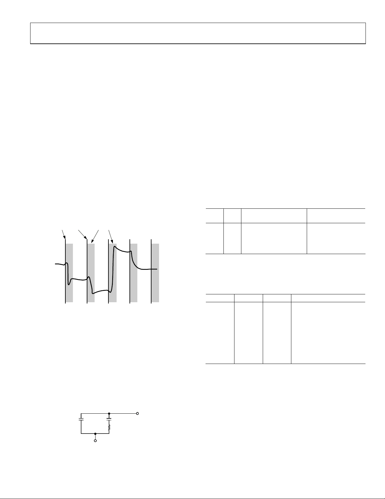
PIXEL CLOC
Figure 6). The ratio of the slewing time
INVALID SAMPLE TIMES
Four programmable registers are provided to optimize the
performance of the PLL. These registers are the 12-Bit Divisor
Register, the 2-Bit VCO Range Register, the 3-Bit Charge Pump
Current Register, and the 5-Bit Phase Adjust Register.
The 12-Bit Divisor Register
The input Hsync frequencies can accommodate any Hsync as
lo
ng as the product of the Hsync and the PLL divisor falls
within the operating range of the VCO. The PLL multiplies the
frequency of the Hsync signal, producing pixel clock
frequencies in the range of 10 MHz to 140 MHz. The divisor
register controls the exact multiplication factor. This register
may be set to any value between 2 and 4095 as long as the
output frequency is within range.
The 2-Bit VCO Range Register
To improve the noise performance of the AD9983A, the VCO
perating frequency range is divided into four overlapping
o
regions. The VCO range register sets this operating range. The
frequency ranges for the four regions are shown in Tab le 8 .
Table 8. VCO Frequency Ranges
Pixel Clock
R
PV1 PV0
0 0 10 to 21 150
0 1 21 to 42 150
1 0 42 to 84 150
1 1 84 to 140 150
ange (MHz)
KVCO
Gain (MHz/V)
The 3-Bit Charge Pump Current Register
This register varies the current that drives the low pass loop
f
ilter. The possible current values are listed in Tab le 9 .
6475-005
Figure 6. Pixel Sampling Times
Any jitter in the clock reduces the precision with which the
sampling time can be determined and must also be subtracted
from the stable pixel time. Considerable care has been taken in
the design of the AD9983A clock generation circuit to
minimize jitter. The clock jitter of the AD9983A is low in all
operating modes, making the reduction in the valid sampling
time due to jitter negligible.
The PLL characteristics are determined by the loop filter design,
he PLL charge pump current, and the VCO range setting. The
t
loop filter design is shown in Figure 7. Recommended settings
o
f the VCO range and charge pump current for VESA standard
display modes are listed in
C
P
.2n
Tabl e 10.
C
Z
82nF
R
Z
1.5kΩ
FILT
Figure 7. PLL Loop Filter Detail
PV
D
06475-006
Table 9. Charge Pump Current/Control Bits
Ip2 Ip1 Ip0 Current (μA)
0 0 0 50
0 0 1 100
0 1 0 150
0 1 1 250
1 0 0 350
1 0 1 500
1 1 0 750
1 1 1 1500
The 5-Bit Phase Adjust Register
The phase of the generated sampling clock can be shifted to
lo
cate an optimum sampling point within a clock cycle. The
phase adjust register provides 32 phase-shift steps of 11.25°
each. The Hsync signal with an identical phase shift is available
through the HSOUT pin. Phase adjust is still available if an
external pixel clock is used. The COAST pin or the internal
coast is used to allow the PLL to continue to run at the same
frequency in the absence of the incoming Hsync signal or
during disturbances in Hsync (such as from equalization
pulses). This can be used during the vertical sync period or at
any other time that the Hsync signal is unavailable.
Rev. 0 | Page 13 of 44

AD9983A
www.BDTIC.com/IC
The polarity of the coast signal may be set through the coast
polarity register (Register 0x18, Bits[6:5]). Also, the polarity of
the Hsync signal can be set through the Hsync polarity register
(Register 0x12, Bits[5:4]). For both Hsync and coast, a value of 1
Table 10. Recommended VCO Range and Charge Pump and Current Settings for Standard Display Formats
Refresh Rate
Standard Resolution
VGA 640 × 480 60 31.500 25.175 800 00 101 0
72 37.700 31.500 832 01 100 0
75 37.500 31.500 840 01 100 0
85 43.300 36.000 832 01 100 0
SVGA 800 × 600 56 35.100 36.000 1024 01 100 0
60 37.900 40.000 1056 01 101 0
72 48.100 50.000 1040 01 101 0
75 46.900 49.500 1056 01 101 0
85 53.700 56.250 1048 01 110 0
XGA 1024 × 768 60 48.400 65.000 1344 10 100 0
70 56.500 75.000 1328 10 101 0
75 60.000 78.750 1312 10 101 0
80 64.000 85.500 1336 10 101 0
85 68.300 94.500 1376 10 110 0
SXGA 1280 × 1024 60 64.000 108.000 1688 10 110 0
75 80.000 135.000 1688 11 110 0
TV 480i 30 15.750 13.510 858 00 101 1
480p 60 31.470 27.000 858 00 101 0
576i 30 15.625 13.500 864 00 101 1
576p 60 31.250 27.000 864 00 101 0
720p 60 45.000 74.250 1650 10 101 0
1035i 30 33.750 74.250 2200 10 101 0
1080i 60 33.750 74.250 2200 10 101 0
(Hz)
Horizontal
F
requency (kHz) Pixel Rate (MHz) PLL Divider
is active high. The internal coast function is driven off the
Vsync signal, which is typically a time when Hsync signals may
be disrupted with extra equalization pulses.
VCO
Range Current
VCO Gear
(R0x36[0])
Rev. 0 | Page 14 of 44

AD9983A
www.BDTIC.com/IC
HSYNC0
HSYNC1
SOGIN0
SOGIN1
VSYNC0
VSYNC1
EXTCK/COAST
AD9983A
ACTIVITY
DETECT
ACTIVITY
DETECT
SYNC SLICER
SYNC SLICER
ACTIVITY
DETECT
ACTIVITY
DETECT
POLARITY
DETECT
POLARITY
DETECT
ACTIVITY
DETECT
ACTIVITY
DETECT
POLARITY
DETECT
POLARITY
DETECT
MUX
MUX
MUX
CHANNEL
SELECT
PROCESSOR
VSYNC FILTER
Figure 8. Sync Processing Block Diagram
SYNC PROCESSING
The inputs of the sync processing section of the AD9983A are
combinations of digital Hsyncs and Vsyncs, analog sync-ongreen, or sync-on-Y signals, and an optional external coast
signal. From these signals it generates a precise, jitter-free clock
from its PLL; an odd/even field signal; HSOUT and VSOUT
signals; a count of Hsyncs per Vsync; and a programmable
SOGOUT. The main sync processing blocks are the sync slicer,
sync separator, Hsync filter, Hsync regenerator, Vsync filter, and
coast generator.
• The sy
• The sy
• The H
nc slicer extracts the sync signal from the green
graphics or luminance video signal that is connected to the
SOGINx input and outputs a digital composite sync.
nc separator’s task is to extract Vsync from the
composite sync signal, which can come from either the sync
slicer or the HSYNCx inputs.
sync filter is used to eliminate any extraneous pulses
from the HSYNCx or SOGINx inputs, outputting a clean,
low jitter signal that is appropriate for mode detection and
clock generation.
SYNC
AND
HSYNC
SELECT
MUX
MUX
COAST
HSYNC FILTER
AND
REGENERATOR
FILTERED
HSYNC
HSYNC/VSYNC
COUNTER
REG 0x26, 0x27
HSYNC
PLL CLOCK
GENERATOR
REGENERATED
HSYNC
MUX
SET
POLARITY
SET
POLARITY
SET
POLARITY
SET
POLARITY
SOGOUT
VSOUT/A0
O/E FIELD
HSOUT
DATACK
he Hsync regenerator is used to recreate a clean, although
• T
not low jitter, Hsync signal that can be used for mode
detection and counting Hsyncs per Vsync.
• The Vsy
nc filter is used to eliminate spurious Vsyncs,
maintain a stable timing relationship between the Vsync and
Hsync output signals, and generate the odd/even field output.
• The co
ast generator creates a robust coast signal that
allows the PLL to maintain its frequency in the absence of
Hsync pulses.
Sync Slicer
The purpose of the sync slicer is to extract the sync signal from
the green graphics or luminance video signal that is connected
to the SOG input. The sync signal is extracted in a two step
process. First, the SOG input is clamped to its negative peak,
(typically 0.3 V below the black level). Next, the signal goes to a
comparator with a variable trigger level (set by Register 0x1D,
Bits[7:3]), but nominally 0.128 V above the clamped level. The
sync slicer output is a digital composite sync signal containing
both Hsync and Vsync information (see
Figure 9).
6475-013
Rev. 0 | Page 15 of 44

AD9983A
S
www.BDTIC.com/IC
NEGATIVE PULSE WIDTH = 40 S AMPLE CLO CKS
700mV MAXIMUM
SOG INPUT
OGOUT OUTPUT
CONNECTED TO
HSYNCIN
COMPOSIT E
SYNC
AT H SY N CI N
VSYNCOUT
FROM SYNC
SEPARATOR
Sync Separator
As part of sync processing, the sync separator’s task is to extract
Vsync from the composite sync signal. It works on the idea that
the Vsync signal stays active for a much longer time than the
Hsync signal. By using a digital low-pass filter and a digital
comparator, it rejects pulses with small durations (such as
Hsyncs and equalization pulses) and only passes pulses with
large durations, such as Vsync (see
The threshold of the digital comparator is programmable for
max
imum flexibility. To program the threshold duration, write
a value (N) to Register 0x11. The resulting pulse width is N ×
200 ns. So, if N = 5, the digital comparator threshold is 1 μs.
Any pulse less than 1 μs is rejected, while any pulse greater than
1 μs passes through.
There are two factors to consider when using the sync separator.
First, the resulting clean Vsync output is delayed from the
original Vsync by a duration equal to the digital comparator
threshold (N × 200 ns). Second, there is some variability to the
200 ns multiplier value. The maximum variability over all
operating conditions is ±20% (160 ns to 240 ns). Since normal
Vsync and Hsync pulse widths differ by a factor of
approximately 500 or more, the 20% variability is not an issue.
Hsync Filter and Regenerator
The Hsync filter is used to eliminate any extraneous pulses from
the Hsync or SOGIN inputs, outputting a clean, low jitter signal
that is appropriate for mode detection and clock generation.
The Hsync regenerator is used to recreate a clean, although not
low jitter, Hsync signal that can be used for mode detection and
counting Hsyncs per Vsync. The Hsync regenerator has a high
+300mV
0mV
–300mV
Figure 9).
Figure 9. Sync Slicer and Sync Separator Output
degree of tolerance to extraneous and missing pulses on the
Hsync input, but is not appropriate for use by the PLL in
creating the pixel clock due to jitter.
The Hsync regenerator runs automatically and requires no
etup to operate. The Hsync filter requires the setting up of a
s
filter window. The filter window sets a periodic window of time
around the regenerated Hsync leading edge where valid Hsyncs
are allowed to occur. The general idea is that extraneous pulses
on the sync input occur outside of this filter window and thus
are filtered out. To set the filter window timing, program a value
(x) into Register 0x23. The resulting filter window time is ±x
times 25 ns around the regenerated Hsync leading edge. Just as
for the sync separator threshold multiplier, allow a ±20%
variance in the 25 ns multiplier to account for all operating
conditions (20 ns to 30 ns range).
A second output from the Hsync filter is a status bit (Register 0x25,
Bit 1) that tells whether extraneous pulses were present on the
incoming sync signal or not. Often, extraneous pulses are
included for copy protection purposes, so this status bit can be
used to detect that.
The filtered Hsync (rather than the raw HSYNCx/SOGINx
al) for pixel clock generation by the PLL is controlled by
sign
Register 0x20, Bit 2. The regenerated Hsync (rather than the
raw Hsync/SOGIN signal) for the sync processing is controlled
by Register 0x20, Bit 1. Use of the filtered Hsync and
regenerated Hsync is recommended. See
i
llustration of a filtered Hsync.
06475-015
Figure 10 for an
Rev. 0 | Page 16 of 44

AD9983A
www.BDTIC.com/IC
HSYNCIN
FILTER
WINDOW
HSYNCOUT
VSYNC
Figure 10. Sync Processing Filter
Vsync Filter and Odd/Even Fields
The Vsync filter is used to eliminate spurious Vsyncs, maintain
a stable timing relationship between the Vsync and Hsync
output signals, and generate the odd/even field output.
The filter works by examining the placement of Vsync with
spect to Hsync and if necessary shifting it in time slightly.
re
The goal is to keep the Vsync and Hsync leading edges from
switching at the same time, thus eliminating confusion as to
when the first line of a frame occurs. Register 0x14, Bit 2
enables the Vsync filter. Use of the Vsync filter is recommended
for all cases, including interlaced video, and is required when
using the Hsyncs per Vsync counter.
llustrate even/odd field determination in two situations.
i
Figure 11 and Figure 12
FILTER
WINDOW
QUADRANT
HSYNCIN
VSYNCIN
VSYNCOUT
O/E FIELD
QUADRANT
HSYNCIN
VSYNCIN
EQUALIZATION
PULSES
EXPECTED
EDGE
06475-016
SYNC SEPARATOR T HRESHOLD
FIELD 1 FIELD 0
23 214431
ODD FIELD
Figure 11. Vsync Filter—Odd Field
SYNC SEPARATOR T HRESHOLD
FIELD 1 FIELD 0
23 214431
FIELD 1 FIELD 0
FIELD 1 FIELD 0
06475-017
VSYNCOUT
O/E FIELD
Rev. 0 | Page 17 of 44
EVEN FIELD
Figure 12. Vsync Filter—Even Field
06475-018

AD9983A
www.BDTIC.com/IC
POWER MANAGEMENT
To meet display requirements for low standby power, the
AD9983A includes a power-down mode. The power-down state
can be controlled manually (via Pin 17 or Register 0x1E, Bit 3),
or automatically by the chip. If automatic control is selected
(Register 0x1E, Bit 4), the AD9983A decision is based on the
status of the sync detect bits (Register 0x24, Bit 2, Bit 3, Bit 6,
and Bit 7). If either an Hsync or a sync-on-green input is
detected on any input, the chip powers up, otherwise it powers
down. For manual control, the AD9983A allows flexibility of
control through both a dedicated pin and a register bit. The
dedicated pin allows a hardware watchdog circuit to control
power-down, while the register bit allows power-down to be
controlled by software. With manual power-down control, the
polarity of the power-down pin must be set (Register 0x1E, Bit 2)
whether the pin is used or not. If unused, it is recommended to
set the polarity to active high and hardwire the pin to ground with
a 10 kΩ resistor.
In power-down mode, there are several circuits that continue to
o
perate as normal. The serial register and sync detect circuits
maintain power so that the AD9983A can be woken up from
its power-down state. The bandgap circuit maintains power
because it is needed for sync detection. The sync-on-green and
SOGOUT functions continue to operate because the SOGOUT
output is needed when sync detection is performed by a
secondary chip. All of these circuits require minimal power to
operate. Typical standby power on the AD9983A is about 50 mW.
There are two options that can be selected when in power-
wn. These are controlled by Bit 0 and Bit 1 in Register 0x1E.
do
Bit 0 controls whether the SOGOUT pin is in high impedance
or not. In most cases, the user will not place SOGOUT in high
impedance during normal operation. The option to put
SOGOUT in high impedance is included mainly to allow for
factory testing modes. Bit 1 keeps the AD9983A powered up
while placing only the outputs in high impedance. This option
is useful when the data outputs from two chips are connected
on a PCB and the user wants to switch instantaneously between
the two.
Table 11. Power-Down Control and Mode Descriptions
Inputs
Mode
Power-Up 1 X 1 Everything
Power-Down 1 X 0
Power-Up 0 0 X Everything
Power-Down 0 1 X
1
Auto power-down control is set by Register 0x1E, Bit 4.
2
Power-down is controlled by OR’ing Pin 17 with Register 0x1E, Bit 3. The polarity of Pin 17 is set by Register 0x1E, Bit 2.
3
Sync detect is determined by OR’ing Register 0x24, Bit 2, Bit 3, Bit 6, and Bit 7.
Auto Power-Down
Co
ntrol
1
Power-Down
2
Sync Detect3Powered On/Comments
Only the serial bus, sync activity detect,
SOG, bandgap ref
Only the serial bus, sync activity detect,
SOG, bandgap ref
erence
erence
TIMING DIAGRAMS
The timing diagrams in Figure 13 to Figure 16 show the operation of the AD9983A. The output data clock signal is created so that its
rising edge always occurs between data transitions and can be used to latch the output data externally. There is a pipeline in the
AD9983A, which must be flushed before valid data becomes available. This means six data sets are presented before valid data is available.
t
PER
t
DCYCLE
DATACK
t
SKEW
DATA
HSOUT
Figure 13. Output Timing
Rev. 0 | Page 18 of 44
06475-007

AD9983A
www.BDTIC.com/IC
DATAIN P0 P1 P2 P5
HSYNCx
DATACK
DATAOUT P0 P1 P2
HSOUT
P3 P4
2 CLOCK CYCLE DELAY
Figure 14. 4:4:4 Timing Mode
DATAIN P0 P1 P2 P5
HSYNCx
DATACK
YOUT Y0 Y1 Y2
CB/CROUT
HSOUT
NOTES
1. PIXEL AFTER HSOUT CORRESONDS TO BLUE INPUT.
2. EVEN NUMBER OF PIXEL DELAY BETWEEN HSOUT AND DATAOUT.
P3 P4
2 CLOCK CYCLE DE LAY
Figure 15. 4:2:2 Timing Mode
DATAIN P0 P1 P2 P5
P3 P4
P9P6
P8 P10 P11P7
8 CLOCK CYCLE DEL AY
P9P6
P8 P10 P11P7
8 CLOCK CYCLE DE LAY
CB0 CR0 CB2 CR2
P9P6
P8 P10 P11P7
P3
06475-008
Y3
06475-009
HSYNCx
DATACK
2 CLOCK CYCLE DE LAY
HSOUT
DDR NOTES
1. OUTPUT DATACK M AY BE DELAYED 1/4 CLOCK PERIOD IN T HE REGIST ERS.
2. SEE PROJECT DOCUMENT F OR VALUES OF F (FALLING EDGE) AND R (RISING EDGE).
3. FOR DDR 4:2:2 MODE: TI MING IS I DENTICAL, VALUES OF F AND R CHANGE.
GENERAL NOTE S
1. DATA DELAY MAY VARY ± ONE CLOCK CYCLE, DEPENDI NG ON PHASE S ETTING .
2. ADCs SAMPLE INPUT ON FALLING EDGE OF DATACK.
3. HSYNC SHOWN I S ACTIVE HIGH (E DGE SHOWN I S LEADING EDGE).
Figure 16. Double Data Rate (DDR) Timing Mode
HSYNC TIMING
The Hsync is processed in the AD9983A to eliminate ambiguity
in the timing of the leading edge with respect to the phasedelayed pixel clock and data.
The Hsync input is used as a reference to generate the pixel
mpling clock. The sampling phase can be adjusted with
sa
respect to Hsync through a full 360° in 32 steps via the phase
adjust register (to optimize the pixel sampling time). Display
systems use Hsync to align memory and display write cycles, so
it is important to have a stable timing relationship between
Hsync output (HSOUT) and the data clock (DATACK).
8 CLOCK CYCLE DE LAY
F0 R0 F1 R1 F2 R2 F3 R3
06475-010
Three things happen to Hsync in the AD9983A. First, the
p
olarity of Hsync input is determined and thus has a known
output polarity. The known output polarity can be programmed
either active high or active low (Register 0x12, Bit 3). Second,
HSOUT is aligned with DATACK and data outputs. Third, the
duration of HSOUT (in pixel clocks) is set via Register 0x13.
HSOUT is the sync signal that should be used to drive the rest
of the display system.
Rev. 0 | Page 19 of 44

AD9983A
www.BDTIC.com/IC
COAST TIMING
In most computer systems, the Hsync signal is provided
continuously on a dedicated wire. In these systems, the coast
input and function are unnecessary and should not be used.
In some systems, however, Hsync is disturbed during the
ertical sync period (Vsync). In some cases, Hsync pulses
v
disappear. In other systems, such as those that employ
composite sync (Csync) signals or embedded sync-on-green,
Hsync may include equalization pulses or other distortions
during Vsync. To avoid upsetting the clock generator during
Vsync, it is important to ignore these distortions. If the pixel
clock PLL sees extraneous pulses, it attempts to lock to this new
frequency, and will have changed frequency by the end of the
Vsync period. It then takes a few lines of correct Hsync timing
to recover at the beginning of a new frame, resulting in a tearing
of the image at the top of the display.
The COAST input is provided to eliminate this problem. It is an
chronous input that disables the PLL input and holds the
asyn
clock at its current frequency. The PLL can free run for several
lines without significant frequency drift. Coast can be generated
internally by the AD9983A (see Register 0x18) or can be
provided externally by the graphics controller.
When internal coast is selected (Register 0x18, Bit 7 = 0, and
Reg
ister 0x14, Bits[7:6] to select source), Vsync is used as a
basis for determining the position of COAST. The internal coast
signal is enabled a programmed number of Hsync periods
before the periodic Vsync signal (Precoast Register 0x16) and
dropped a programmed number of Hsync periods after Vsync
(Postcoast Register 0x17). It is recommended that the Vsync
filter be enabled when using the internal coast function to allow
the AD9983A to determine precisely the number of Hsyncs/Vsync
and their location. In many applications where disruptions
occur and coast is used, values of 2 for Precoast and 10d for
Postcoast are sufficient to avoid most extraneous pulses.
OUTPUT FORMATTER
The output formatter is capable of generating several output
formats to be presented to the 24 data output pins. The output
formats and the pin assignments for each format are listed in
Tabl e 1 2 . Also, there are several clock options for the output
ck. The user may select the pixel clock, a 90° phase-shifted
clo
pixel clock, a 2× pixel clock, or a fixed frequency 40 MHz clock
for test purposes. The output clock may also be inverted.
Data output is available as 24-pin RGB or YCbCr, or if either
4:2:2 o
r 4:4:4 DDR is selected, a secondary channel is available.
This secondary channel is always 4:2:2 DDR and allows the
flexibility of having a second channel with the same video data
that can be utilized by either another display or even a storage
device. Depending on the choice of output modes, the primary
output can be 24 pins, 16 pins, or as little as 12 pins.
Mode Descriptions
4:4:4
All channels come out with their 8 data bits at the same time.
Da
ta is aligned to the negative edge of the clock for easy capture.
This is the normal 24-bit output mode for RGB or 4:4:4 YCbCr.
4:2:2
Red and green channels contain 4:2:2 formatted data (16 pins)
with Y data on the green channel and Cb, Cr data on the red
channel. Data is aligned to the negative edge of the clock. The
blue channel contains the secondary channel with Cb, Y, Cr, Y
formatted 4:2:2 DDR data. The data edges are aligned to both
edges of the pixel clock, so use of the 90° clock may be necessary to
capture the DDR data.
4:4:4 DDR
This mode puts out full 4:4:4 data on 12 bits of the red and
green channels, thus saving 12 pins. The first half (RGB[11:0])
of the 24-bit data is sent on the rising edge and the second half
(RGB[23:12]) is sent on the falling edge. DDR 4:2:2 data is sent
on the blue channel, as in 4:2:2 mode.
RGB [23:0] = R [7:0] + G [7:0] + B [7:0], so
GB [23:12] = R [7:0] + G [7:4] and
R
RGB [11:0] = G [3:0] + B [7:0]
Table 12. Output Formats
Port Red Green Blue
Bit 7 6 5 4 3 2 1 0 7 6 5 4 3 2 1 0 7 6 5 4 3 2 1 0
4:4:4 Red/Cr Green/Y Blue/Cb
1
4:2:2
4:4:4 DDR
1
For 4:2:2 Cb sent before Cr.
2
Arrows in table indicate clock edge. Rising edge of clock = ↑, falling edge = ↓.
2
G [3:0] DDR ↑ B [7:4] DDR ↑ B [3:0]
DDR ↑
Cb, Cr Y DDR 4:2:2 ↑ Cb, Cr ↓ Y, Y
N/A
2
R [7:0] DDR ↓ G [7:4]
DDR ↓
Rev. 0 | Page 20 of 44
N/A
DDR 4:2:2 ↑ Cb, Cr
DDR 4:2:2 ↓ Y, Y

AD9983A
S
C
www.BDTIC.com/IC
2-WIRE SERIAL CONTROL PORT
A 2-wire serial interface control interface is provided. Up to two
AD9983A devices may be connected to the 2-wire serial
interface, with each device having a unique address.
The 2-wire serial interface comprises a clock (SCL) and a bi-
ectional data (SDA) pin. The analog flat panel interface acts
dir
as a slave for receiving and transmitting data over the serial
interface. When the serial interface is not active, the logic levels
on SCL and SDA are pulled high by external pull-up resistors.
Data received or transmitted on the SDA line must be stable for
e duration of the positive-going SCL pulse. Data on SDA must
th
change only when SCL is low. If SDA changes state while SCL is
high, the serial interface interprets that action as a start or stop
sequence.
The following are the five components to serial bus operation:
art signal
• St
• Sla
ve address byte
• B
ase register address byte
• Da
ta byte to read or write
• Stop
signal
When the serial interface is inactive (SCL and SDA are high),
co
mmunications are initiated by sending a start signal. The start
signal is a high-to-low transition on SDA while SCL is high.
This signal alerts all slaved devices that a data transfer sequence
is coming.
The first 8 bits of data transferred after a start signal comprise a
it slave address (the first 7 bits) and a single R/
7-b
eighth bit). The R/
W
bit indicates the direction of data transfer,
W
bit (the
read from 1 or write to 0 on the slave device. If the transmitted
slave address matches the address of the device, the AD9983A
acknowledges the match by bringing SDA low on the ninth SCL
pulse. If the addresses do not match, the AD9983A does not
acknowledge it.
Table 13. Serial Port Addresses
Bit 7 Bit 6 Bit 5 Bit 4 Bit 3 Bit 2 Bit 1
A6 (MSB) A5 A4 A3 A2 A1 A0
1 0 0 1 1 0 0
1 0 0 1 1 0 1
DATA TRANSFER VIA SERIAL INTERFACE
For each byte of data read or written, the MSB is the first bit in
the sequence.
If the AD9983A does not acknowledge the master device during
a wr
ite sequence, the SDA remains high so the master can generate a stop signal. If the master device does not acknowledge
the AD9983A during a read sequence, the AD9983A interprets
this as end of data. The SDA remains high so the master can
generate a stop signal.
Writing data to specific control registers of the AD9983A
r
equires writing to the 8-bit address of the control register of
interest after the slave address has been established. This control
register address is the base address for subsequent write
operations. The base address auto-increments by one for each
byte of data written after the data byte intended for the base
address. If more bytes are transferred than there are available
addresses, the address does not increment and remains at its
maximum value of 0x2E. Any base address higher than 0x2E
will not produce an acknowledge signal. Data are read from the
control registers of the AD9983A in a similar manner. Reading
requires two data transfer operations:
W
The base address must be written with the R/
address byte low to set up a sequential read operation. Reading
W
(the R/
bit of the slave address byte high) begins at the
previously established base address. The address of the read
register auto-increments after each byte is transferred.
To terminate a read/write sequence to the AD9983A, a stop
sig
nal must be sent. A stop signal comprises a low-to-high
transition of SDA while SCL is high.
A repeated start signal occurs when the master device driving
he serial interface generates a start signal without first genera-
t
ting a stop signal to terminate the current communication. This
is used to change the mode of communication (read, write)
between the slave and master without releasing the serial
interface lines.
bit of the slave
DA
t
BUFF
t
STAH
L
S
t
DHO
t
DAL
t
DSU
t
DAH
Figure 17. Serial Port Read/Write Timing
t
STASU
Rev. 0 | Page 21 of 44
t
STOSU
06475-011

AD9983A
www.BDTIC.com/IC
Serial Interface Read/Write Examples
Write to One Control Register
1. Start signal
ve address byte (R/
2. Sla
ase address byte
3. B
4. Da
ta byte to base address
5. Stop
signal
W
bit = low)
Write to Four Consecutive Control Registers
1. Start signal
ve address byte (R/
2. Sla
ase address byte
3. B
4. Da
ta byte to base address
5. D
ata byte to (base address + 1)
6. D
ata byte to (base address + 2)
7. D
ata byte to (base address + 3)
8. Stop
signal
W
bit = low)
BIT 7
Read from One Control Register
1. Start signal
2. Sla
ve address byte (R/
ase address byte
3. B
4. St
art signal
ve address byte (R/
5. Sla
6. Da
ta byte from base address
7. Stop
signal
W
bit = low)
W
bit = high)
Read from Four Consecutive Control Registers
1. Start signal
ve address byte (R/
2. Sla
3. B
ase address byte
4. St
art signal
ve address byte (R/
5. Sla
6. Da
ta byte from base address
7. D
ata byte from (base address + 1)
8. D
ata byte from (base address + 2)
9. D
ata byte from (base address + 3)
10. Stop
signal
W
bit = low)
W
bit = high)
ACKBIT 6 BIT 5 BIT 4 BIT 3 BIT 2 BIT 1 BIT 0SDA
SCL
Figure 18. Serial Interface—Typical Byte Transfer
06475-012
Rev. 0 | Page 22 of 44

AD9983A
www.BDTIC.com/IC
2-WIRE SERIAL REGISTER MAP
The AD9983A is initialized and controlled by a set of registers that determine the operating modes. An external controller is employed to
write and read the control registers through the 2-wire serial interface port.
Table 14. Control Register Map
Hex
Address
0x00 RO 7:0 Chip Revision An 8-bit register that represents the silicon revision level.
0x01
0x02
0x03
5:3 **00 1***
2 **** *0** External Clock Enable.
0x04
0x05
0x06
0x07
0x08
0x09
0x0A
0x0B
0x0C
0x0D
0x0E
0x0F
0x10
0x11
Read/Write,
Read Only Bits
R/W
R/W
R/W
R/W
R/W
R/W
R/W
R/W
R/W
R/W
R/W
R/W
R/W
R/W
R/W
R/W
R/W
7:0 0110 1001 PLL Div MSB
7:4 1101 **** PLL Div LSB
7:6 01** **** VCO/CPMP VCO Range. Selects VCO frequency range. (See PLL section).
7:3 1000 0*** Phase Adjust
6:0 *100 0000 Red Gain MSB
7:0 0000 0000
6:0 *100 0000 Green Gain MSB
7:0 0000 0000
6:0 *100 0000 Blue Gain MSB
7:0 0000 0000
7:0 0100 0000 Red Offset MSB
7 0*** **** Red Offset LSB
7:0 0100 0000 Green Offset MSB
7 0*** **** Green Offset LSB
7:0 0100 0000 Blue Offset MSB
7 0*** **** Blue Offset LSB
7:0 0010 0000
Default
Value Register Name Description
This register is for Bits [11:4] of the PLL divider. Larger values mean
ates at a faster rate. This register should be loaded first
1
1
egister.
T/32).
2
tion.
2
tion.
2
tion.
1
set (brightness) of the red channel in auto-offset mode.
brightness) of each respective channel. Bigger values
1
set (brightness) of the blue channel in auto-offset mode.
Sync Separator
eshold
Thr
the PLL oper
whenever a change is needed. (This will give the PLL more time to
lock).
LSBs of the PLL Divider Word. Links to the PLL Div MSB to make a
12-bit r
Charge Pump Current. Varies the curr
filter. (See PLL section).
ADC Clock Phase Adjustment. Larger values mean more delay.
(1 LSB =
7-Bit Red Channel Gain Control. Controls the ADC input range
ontrast) of each respective channel. Bigger values give less
(c
contrast.
Must be written to 0x00 following a write of Reg. 0x05 for proper
opera
7-Bit Green Channel Gain Control. Controls the ADC input range
ontrast) of each respective channel. Bigger values give less
(c
contrast.
Must be written to 0x00 following a write of Reg. 0x07 for proper
opera
7-Bit Blue Channel Gain Control. Controls the ADC input range
ontrast) of each respective channel. Bigger values give less
(c
contrast.
Must be written to 0x00 following a write of Reg. 0x09 for proper
opera
8-Bit MSB of the Red Channel Offset Control. Controls the dc offset
ightness) of each respective channel. Bigger values decrease
(br
brightness.
Linked with Reg. 0x0B to form the 9-bit red offset that controls the
dc off
8-Bit MSB of the Green Channel Offset Control. Controls the dc
offset (
decrease brightness.
Linked with Reg. 0x0D to form the 9-bit green offset that controls
dc offset (brightness) of the green channel in auto-offset mode.
the
8-Bit MSB of the Red Channel Offset Control. Controls the dc offset
ightness) of each respective channel. Bigger values decrease
(br
brightness.
Linked with Reg. 0x0F to form the 9-bit blue offset that controls the
dc off
This register sets the threshold of the sync separator’s digital
comparator.
ent that drives the low-pass
1
Rev. 0 | Page 23 of 44

AD9983A
www.BDTIC.com/IC
Hex
Address
0x12
6 *0** ****
5 **0* ****
4 ***1 ****
3 **** 1***
0x13
0x14
6 *0** ****
5 **0* ****
4 ***1 ****
3 **** 1***
2 **** *0**
1 **** **0*
0x15
0x16
0x17
0x18
6 *0** ****
5 **1* ****
Read/Write,
Read Only Bits
R/W
R/W
R/W
R/W
R/W
R/W
R/W
7 0*** **** Hsync Control
7:0 0010 0000 Hsync Duration Sets the number of pixel clocks that HSOUT is active.
7 0*** **** Vsync Control
7:0 0000 1010 Vsync Duration
7:0 0000 0000 Precoast The number of Hsync periods to coast prior to Vsync.
7:0 0000 0000 Postcoast The number of Hsync periods to coast after Vsync.
7 0*** ****
Default
Value Register Name Description
Active Hsync Override.
The chip determines the active Hsync source
0 =
1 = The active Hsync source is set by Reg. 0x12, Bit 6
Selects the source of the Hsync for PLL and sync processing. This bit is
d only if Reg. 0x12, Bit 7 is set to 1 or if both syncs are active.
use
0 = Hsync is from HSYNCx input pin
1 = Hsync is from SOGINx
Hsync Input Polarity Override.
The chip selects the Hsync input polarity
0 =
1 = The polarity of the input Hsync is controlled by Reg. 0x12, Bit 4
This applies to both HSYNC0 and HSYNC1.
Hsync Input Polarity. This bit is used only if
0 = Active low input Hsync
1 = Active high input Hsync
Sets the polarity of the Hsync output signal.
ctive low Hsync output
0 = A
1 = Active high Hsync output
Active Vsync Override.
The chip determines the active Vsync source
0 =
1 = The active Vsync source is set by Reg. 0x14, Bit 6
Selects the source of Vsync for the sync processing. This bit is used
eg. 0x14, Bit 7 is set to 1.
only if R
0 = Vsync is from the Vsync input pin
1 = Vsync is from the sync separator
Vsync Input Polarity Override. This applies to both VSYNC0 and
NC1.
VSY
0 = The chip selects the input Vsync polarity
1 = The polarity of the input Vsync is set by Reg. 0x14, Bit 4
Vsync Input Polarity. This bit is used only if Reg. 0x14, Bit 5 is set to 1.
ctive low input Vsync
0 = A
1 = Active high input Vsync
Sets the polarity of the output Vsync signal.
ctive low output Vsync
0 = A
1 = Active high output Vsync
Vsync Filter Enable. This needs to be enabled when using the
o Vsync counter.
Hsync t
0 = The Vsync filter is disabled
1 = The Vsync filter is enabled
Enables the Vsync duration block. This is designed to be used with
sync filter.
the V
0 = Vsync output duration is unchanged
1 = Vsync output duration is set by Reg. 0x15
Sets the number of Hsyncs that Vsync out is ac
used if Reg. 0x14, Bit 1 is set to 1.
Coast and Clamp
ntrol
Co
Coast Source. Selects the source of the coast signal.
0 = Using internal coast generated from Vsync
1 = Using external coast signal from external COAST pin
Coast Polarity Override.
The chip selects the external coast polarity
0 =
1 = The polarity of the external coast signal is set by Reg. 0x18, Bit 5
Coast Input Polarity. This bit is used only if Reg. 0x18, Bit 6 is set to 1.
ctive low external coast
0 = A
1 = Active high external coast
Reg. 0x12, Bit 5 is set to 1.
tive. This is only
Rev. 0 | Page 24 of 44

AD9983A
www.BDTIC.com/IC
Hex
Address
4 ***0 ****
3 **** 0***
2 **** *0**
1 **** **0*
0 **** ***0 Must be set to 0 for proper operation.
0x19
0x1A
0x1B
6 *1** ****
5 **0* ****
4:3 ***1 1***
2:0 **** *011 Must be written to default (011) for proper operation.
0x1C
0x1D
2 **** *0**
1:0 **** **00
0x1E
6 *0** ****
5 **1* ****
4 ***1 ****
Read/Write,
Read Only Bits
R/W
R/W
R/W
R/W
R/W
R/W
7:0 0000 1000 Clamp Placement
7:0 0010 0000 Clamp Duration Number of clock periods that the clamp signal is actively clamping.
7 0*** **** Clamp and Offset
7:0 1111 1111 TestReg0 Must be set to 0xFF for proper operation.
7:3 0111 1*** SOG Control
7 *** **** Power
Default
Value Register Name Description
Clamp Source Select.
se the internal clamp generated from Hsync
0 = U
1 = Use the external clamp signal
Red Clamp Select.
0 = Clamp the r
1 = Clamp the red channel to midscale
Green Clamp Select.
0 = Clamp the gr
1 = Clamp the green channel to midscale
Blue Clamp Select.
0 = Clamp the b
1 = Clamp the blue channel to midscale
Places the clamp signal an integer number of clock periods after
ailing edge of the Hsync signal.
the tr
External Clamp Polarity Override.
The chip selects the clamp polarity
0 =
1 = The polarity of the clamp signal is set by Reg. 0x1B, Bit 6
External Clamp Input Polarity. This bit is used only if
is set to 1.
0 = Active low external clamp
1 = Active high external clamp
Auto-Offset Enable.
uto-offset is disabled
0 = A
1 = Auto-offset is enabled (offsets become the desired clamp code)
Auto-Offset Update Frequency. This selects how often the autooffset cir
00 = every 3 clamps
01 = 48 clamps
10 = every 192 clamps
11 = every 3 Vsyncs
SOG Slicer Threshold. Sets the voltage level of the SOG slicer’s
mparator.
co
SOGOUT Polarity. Sets the polarity of th
0 = Active low SOGOUT
1 = Active high SOGOUT
SOGOUT Select.
aw SOG from sync slicer (SOGIN0 or SOGIN1)
00 = R
01 = Raw Hsync (HSYNC0 or HSYNC1)
10 = Regenerated sync from sync filter
11 = Filtered sync from sync filter
Channel Select Override.
The chip determines which input channels to use
0 =
1 = The input channel selection is determined by Reg. 0x1E, Bit 6
Channel Select. Input channel select: this is use
Bit 7 is set to 1, or if syncs are present on both channels.
0 = Channel 0 syncs and data are selected
1 = Channel 1 syncs and data are selected
Programmable Bandwidth.
ow analog input bandwidth (7 MHz)
0 = L
1 = High analog input bandwidth
Power-Down Control Select.
anual power-down control
0 = M
1 = Auto power-down control
ed channel to ground
een channel to ground
lue channel to ground
cuit operates.
Reg. 0x1B, Bit 7
e signal on the SOGOUT pin.
d only if Reg. 0x1E,
Rev. 0 | Page 25 of 44

AD9983A
www.BDTIC.com/IC
Hex
Address
3 **** 0***
2 **** *0**
1 **** **0*
0 **** ***0
0x1F
4 ***1 ****
3 **** 0***
2:1 **** *10*
0 **** ***0
0x20
5 *0** ****
4 **0* ****
3 ***0 ****
2 **** 1***
1 **** *0**
0 Must be set to 1 for proper operation.
0x21
0x22
Read/Write,
Read Only Bits
R/W
R/W
R/W
R/W
7:5 100* **** Output Select 1
7:6 0*** **** Output Select 2
7:0 0010 0000 Must be set to default for proper operation.
7:0 0011 0010 Must be set to default for proper operation.
Default
Value Register Name Description
Power-Down.
mal operation
0 = Nor
1 = Power-down
Power-Down Pin Polarity.
ctive low
0 = A
1 = Active high
Power-Down Fast Switching Control.
mal power-down operation
0 = Nor
1 = The chip stays powered up and the outputs are put in high
impedance mode
SOGOUT High Impedance Control.
0 = SOGOUT oper
1 = SOGOUT is in high impedance during power-down
Output Mode.
100 = 4:4:4 output mode
101 = 4:2:2 output mode
110 = 4:4:4—DDR output mode
Primary Output Enable.
rimary output is in high impedance state
0 = P
1 = Primary output is enabled
Secondary Output Enable.
ondary output is in high impedance state
0 = Sec
1 = Secondary output is enabled
Output Drive Strength.
ow output drive strength
00 = L
01 = Medium output drive strength
10 = High output drive strength
11 = High output drive strength
Applies to all outputs except VSOUT.
Output Clock Invert.
0 = Nonin
1 = Inverted pixel clock
Applies to all clocks output on DATACK.
Output Clock Select.
00 = P
01 = 90° phase shifted pixel clock
10 = 2× pixel clock
11 = 0.5× pixel clock
Output High Impedance.
0 = Normal outputs
1 = All outputs ex
SOG High Impedance.
0 = Normal SOG output
1 = SOGOUT pin
Field Output Polarity. Sets the polarit
0 = Active low => even field, active high => odd field
1 = Active low => odd field, active high => even field
PLL Sync Filter Enable.
0 = PLL uses r
1 = PLL uses filtered Hsync/SOG
Sync Processing Input Select. Selects the sync source for the sync
pr
0 = Sync processing uses raw Hsync/SOGIN
1 = Sync processing uses regenerated Hsync from sync filter
verted pixel clock
ixel clock
ocessor.
ates as normal during power-down
cept SOGOUT in high impedance mode
is in high impedance mode
aw Hsync/SOG
y of the field output signal.
Rev. 0 | Page 26 of 44

AD9983A
www.BDTIC.com/IC
Hex
Address
0x23
0x24 RO 7 _*** **** Sync Detect
6 *_** ****
5 **_* ****
4 ***_ ****
3 **** _***
2 **** *_**
1 **** **_*
0 **** ***_
0x25 RO 7 _*** ****
6 *_** ****
5 **_* ****
4 ***_ ****
3 **** _***
2 **** *_**
1 **** **_*
0
0x26 RO 7:0
0x27 RO 7:4
0x28
0x29
0x2A RO 7:0 TestReg3 Read-only bits for future use.
0x2B RO 7:0 TestReg4 Read-only bits for future use.
Read/Write,
Read Only Bits
R/W
R/W
R/W
7:0 0000 1010
7:0 1011 1111 TestReg1 Must be written to Reg. 0xBF for proper operation.
7:0 0000 0010 TestReg2 Must be written to Reg. 0x02 for proper operation.
Default
Value Register Name Description
Sync Filter
ndow Width
Wi
Sync Polarity
tect
De
Hsyncs Per Vsync
MSBs
Hsyncs Per Vsync
LSBs
Rev. 0 | Page 27 of 44
Sets the window of time around the regenerated Hsync leading
edge (in 25 ns steps) that sync pulses are allowed to pass through.
HSYNC0 Detection Bit.
NC0 is not active
0 = HSY
1 = HSYNC0 is active
HSYNC1 Detection Bit.
NC1 is not active
0 = HSY
1 = HSYNC1 is active
VSYNC0 Detection Bit.
VSYNC0 is not active
0 =
1 = VSYNC0 is active
VSYNC1 Detection Bit.
VSYNC1 is not active
0 =
1 = VSYNC1 is active
SOGIN0 Detection Bit
0 = SOGIN0 is not ac
1 = SOGIN0 is active
SOGIN1 Detection Bit
0 = SOGIN1 is not ac
1 = SOGIN1 is active
COAST Detection Bit.
ternal COAST is not active
0 = Ex
1 = External COAST is active
CLAMP Detection Bit.
ternal CLAMP is not active
0 = Ex
1 = External CLAMP is active
HSYNC0 Polarity.
0 = HSYNC0 polarity is active low
1 = HSYNC0 polarity is active high
HSYNC1 Polarity.
0 = HSYNC1 polar
1 = HSYNC1 polarity is active high
VSYNC0 Polarity.
VSYNC0 polarity is active low
0 =
1 = VSYNC0 polarity is active high
VSYNC1 Polarity.
0 =
VSYNC1 polarity is active low
1 = VSYNC1 polarity is active high
COAST Polarity.
ternal COAST polarity is active low
0 = Ex
1 = External COAST polarity is active high
CLAMP Polarity.
ternal CLAMP polarity is active low
0 = Ex
1 = External CLAMP polarity is active high
Extraneous Pulses Detected.
0 = No ex
1 = Extraneous pulses detected on HSYNCx
Sync Filter Lock
0 = Sync filter unloc
1 = Sync filter locked
MSBs of Hsyncs per Vsync count.
LSBs of Hsyncs per Vsync count.
traneous pulses detected on HSYNCx
ity is active low
tive
tive
ked

AD9983A
www.BDTIC.com/IC
Hex
Address
0x2C
4 ***0 ****
3:0 **** 0000 Must be written to default for proper operation.
0x2D
0x2E
0x34
0x36
0x3C
3 **** 0*** Auto Gain Matching Hold
2:0 **** *000 Auto Gain Matching Enable
1
Functions with more than eight control bits, such as PLL divide ratio, gain, and offset, are only updated when the LSBs are written to (for example, Register 0x02 for
PLL divide ratio).
2
Gain registers (Register 0x05, Register 0x07, and Register 0x09) when written must each be followed with a write to their next register: Register 0x05 and Register 0x06,
Register 0x07, and Register 0x08, and Register 0x09 and Register 0x0A.
Read/Write,
Read Only Bits
R/W
R/W
R/W
R/W
R/W
R/W
7:5 000* **** Offset Hold Must be written to default for proper operation.
7:0 1111 0000 TestReg5 Must be written to Reg. 0xE8 for proper operation.
7:0 1111 0000 TestReg6 Must be written to Reg. 0xE0 for proper operation.
2 **** *0** SOG Filter SOG Filter Enable.
0 **** ***0 VCO Gear
7:4 0000 **** Auto Gain Must be set to default for proper operation
Default
Value Register Name Description
Auto-Offset Hold.
es the auto-offset and holds the feedback result.
Disabl
0 = One time update
1 = Continuous update
0 = Disable SOG filter
1 = Enable SOG filter
VCO Gear adds another range to the VCO—used for lower
equencies only.
fr
0 = Disable low VCO gear
1 = Enable low VCO gear
0 = Disables auto gain updates and holds the current auto offset
lues.
va
1 = Allows auto gain to update continuously
000 = Auto gain is disabled
110= Auto gain is enabled
Rev. 0 | Page 28 of 44

AD9983A
www.BDTIC.com/IC
2-WIRE SERIAL CONTROL REGISTERS
CHIP IDENTIFICATION
0x00—Bits[7:0] Chip Revision
An 8-bit register that represents the silicon revision.
PLL DIVIDER CONTROL
0x01—Bits[7:0] PLL Divide Ratio MSBs
The 8 MSBs of the 12-bit PLL divide ratio PLLDIV.
The PLL derives a pixel clock from the incoming Hsync signal.
T
he pixel clock frequency is then divided by an integer value,
such that the output is phase-locked to Hsync. This PLLDIV
value determines the number of pixel times (pixels plus
horizontal blanking overhead) per line. This is typically 20% to
30% more than the number of active pixels in the display.
The 12-bit value of the PLL divider supports divide ratios from
2 t
o 4095 as long as the output frequency is within range. The
higher the value loaded in this register, the higher the resulting
clock frequency with respect to a fixed Hsync frequency.
VESA has established some standard timing specifications,
which wil
function of horizontal and vertical display resolution and frame
rate (see
co
should be used only as a guide. The display system manufacturer
should provide automatic or manual means for optimizing
PLLDIV. An incorrectly set PLLDIV usually produces one or
more vertical noise bars on the display. The greater the error,
the greater the number of bars produced.
The power-up default value of PLLDIV is 1693. PLLDIVM =
0x69, P
The AD9983A updates the full divide ratio only when the LSBs
a
re written. Writing to this register by itself does not trigger
an update.
l assist in determining the value for PLLDIV as a
Table 1 0). However, many computer systems do not
nform precisely to the recommendations and these numbers
LLDIVL = 0xDX.
0x02—Bits[7:4] PLL Divide Ratio LSBs
The 4 LSBs of the 12-bit PLL divide ratio PLLDIV.
The power-up default value of PLLDIV is 1693.
P
LLDIVM = 0x69, PLLDIVL = 0xDX.
CLOCK GENERATOR CONTROL
0x03—Bits[7:6] VCO Range Select
Two bits that establish the operating range of the clock
generator. VCO range must be set to correspond to the desired
operating frequency (incoming pixel rate). The PLL gives the
best jitter performance at high frequencies. For this reason, in
order to output low pixel rates and still get good jitter performance,
the PLL actually operates at a higher frequency but then divides
down the clock rate afterwards. See
f
or each VCO range setting. The PLL output divisor is automatically selected with the VCO range setting. The power-up
default value is 01.
Tabl e 15 for the pixel rates
Table 15. VCO Ranges
VCO Range Results (Pixel Rates)
00 10 to 21
01 21 to 42
10 42 to 84
11 84 to 140
0x03—Bits[5:3] Charge Pump Current
Three bits that establish the current driving the loop filter in the
clock generator. The current must be set to correspond with the
desired operating frequency. The power-up default value is
current = 001.
Table 16. Charge Pump Currents
Ip2 Ip1 Ip0 Results (Current)
0 0 0 50
0 0 1 100
0 1 0 150
0 1 1 250
1 0 0 350
1 0 1 500
1 1 0 750
1 1 1 1500
0x03—Bit[2] External Clock Enable
This bit determines the source of the pixel clock.
Table 17. External Clock Select Settings
EXTCK Function
0 Internally generated clock
1 Externally provided clock signal
A Logic 0 enables the internal PLL that generates the pixel clock
from an externally provided Hsync.
A Logic 1 enables the external EXTCK input pin. In this mode,
t
he PLL Divide Ratio (PLLDIV) is ignored. The clock phase
adjust (Phase) is still functional. The power-up default value is
EXTCK = 0.
PHASE ADJUST
0x04—Bits[7:3]
Phase adjustment for the DLL to generate the ADC clock. A 5-bit
value that adjusts the sampling phase in 32 steps across one
pixel time. Each step represents an 11.25° shift in sampling
phase. The power up default is 16.
Rev. 0 | Page 29 of 44

AD9983A
www.BDTIC.com/IC
INPUT GAIN
0x05—Bits[6:0] Red Channel Gain Adjust
The 7-Bit Red Channel Gain Control. The AD9983A can
accommodate input signals with a full-scale range of between
0.5 V and 1.0 V p-p. Setting the red gain to 127 corresponds to
an input range of 1.0 V. A red gain of 0 establishes an input
range of 0.5 V. Note that increasing red gain results in the
picture having less contrast (the input signal uses fewer of the
available converter codes). Values written to this register do not
update until the following register (Register 0x06) has been
written to 0x00. The power-up default is 100 0000.
0x07—Bits[6:0] Green Channel Gain Adjust
The 7-Bit Green Channel Gain Control. See red channel gain adjust
above. Register update requires writing 0x00 to Register 0x08.
0x09—Bits[6:0] Blue Channel Gain Adjust
The 7-Bit Blue Channel Gain Control. See red channel gain adjust
above. Register update requires writing 0x00 to Register 0x0A.
INPUT OFFSET
0x0B—Bits[7:0] Red Channel Offset
The 8-Bit MSB of the Red Channel Offset Control. Along with
the LSB in the following register, there are 9 bits of dc offset
control in the red channel. The offset control shifts the analog
input, resulting in a change in brightness. Note that the function
of the offset register depends on whether auto-offset is enabled
(Register 0x1B, Bit 5).
If auto-offset is disabled, the lower 7 bits of the offset registers
(f
or the red channel Register 0x0B, Bits [5:0] plus Register 0x0C,
Bit 7) control the absolute offset added to the channel. The
offset control provides a ±63 LSBs of adjustment range, with 1 LSB
of offset corresponding to 1 LSB of output code.
If auto-offset is enabled, the 9-bit offset (comprised of the 8 bits
f the MSB register and Bit 7 of the following register) determines
o
the clamp target code. The 9-bit offset consists of 1 sign bit
plus 8 bits. If the register is programmed to 130d, then the
output code is equal to 130d at the end of the clamp period.
Incrementing the offset register setting by 1 LSB adds 1 LSB of
offset, regardless of the auto-offset setting. Values written to this
register are not updated until the LSB register (Register 0x0C)
has also been written.
0x0C—Bit[7] Red Channel Offset LSB
The LSB of the red channel offset control combines with the 8 bits
of MSB in the previous register to make 9 bits of offset control.
0x0D—Bits[7:0] Green Channel Offset
The 8-Bit Green Channel Offset Control. See red channel offset
(0x0B). Update of this register occurs only when Register 0x0E
is also written.
0x0E—Bit[7] Green Channel Offset LSB
The LSB of the green channel offset control combines with the
8 bits of MSBs in the previous register to make 9 bits of offset
control.
0x0F—Bits[7:0] Blue Channel Offset
The 8-Bit Blue Channel Offset Control. See 0x0B—Bits[7:0]
Red Channel Offset. Update of this register occurs only when
ister 0x10 is also written.
Reg
0x10—Bit[7] Blue Channel Offset LSB
The LSB of the blue channel offset control combines with the
8 bits of MSB in the previous register to make 9 bits of offset
control.
HSYNC CONTROLS
0x11—Bits[7:0] Sync Separator Threshold
This register sets the threshold of the sync separator’s digital
comparator. The value written to this register is multiplied by
200 ns to get the threshold value. Therefore, if a value of 5 is
written, the digital comparator threshold is 1 μs and any pulses
less than 1 μs are rejected by the sync separator. There is some
variability to the 200 ns multiplier value. The maximum
variability over all operating conditions is ±20% (160 ns to 240 ns).
Since normal Vsync and Hsync pulse widths differ by a factor of
about 500 or more, the 20% variability is not an issue. The
power-up default value is 32 DDR.
0x12—Bit[7] Hsync Source Override
This is the active Hsync override. Setting this to 0 allows the
chip to determine the active Hsync source. Setting it to 1 uses
Bit 6 of Register 0x12 to determine the active Hsync source.
Power-up default value is 0.
Table 18. Active Hsync Source Override
Override Result
0 Hsync source determined by chip
1
0x12—Bit[6] Hsync Source
This bit selects the source of the Hsync for PLL and sync
processing—only if Bit 7 of Register 0x12 is set to 1 or if both
syncs are active. Setting this bit to 0 specifies the Hsync from
the input pin. Setting it to 1 selects Hsync from SOG. Power-up
default is 0.
Table 19. Active Hsync Select Settings
Select Result
0 Hsync input
1 Hsync from SOG
Hsync source determined by user
egister 0x12, Bit 6
R
Rev. 0 | Page 30 of 44

AD9983A
www.BDTIC.com/IC
0x12—Bit[5] Hsync Input Polarity Override
This bit determines whether the chip selects the Hsync input
polarity or if it is specified. Setting this bit to 0 allows the chip
to automatically select the polarity of the input Hsync; setting it
to 1 indicates that Bit 4 of Register 0x12 specifies the polarity.
Power-up default is 0.
Table 20. Hsync Input Polarity Override Settings
Override Bit Result
0 Hsync polarity determined by chip
1
Hsync polarity determined by user
egister 0x12, Bit 4
R
0x12—Bit[4] Hsync Input Polarity
If Bit 5 of Register 0x12 is 1, the value of this bit specifies the
polarity of the input Hsync. Setting this bit to 0 indicates an
active low Hsync; setting this bit to 1 indicates an active high
Hsync. Power-up default is 1.
Table 21. Hsync Input Polarity Settings
Hsync Polarity Bit Result
0 Hsync input polarity is negative
1 Hsync input polarity is positive
0x12—Bit[3] Hsync Output Polarity
This bit sets the polarity of the Hsync output. Setting this bit to
0 sets the Hsync output to active low. Setting this bit to 1 sets
the Hsync output to active high. Power-up default setting is 1.
Table 22. Hsync Output Polarity Settings
Hsync Output
Polarity Bit Result
0 Hsync output polarity is negative
1 Hsync output polarity is positive
0x13—Bits[7:0] Hsync Duration
An 8-bit register that sets the duration of the Hsync output
pulse. The leading edge of the Hsync output is triggered by the
internally-generated, phase-adjusted PLL feedback clock. The
AD9983A then counts a number of pixel clocks equal to the
value in this register. This triggers the trailing edge of the Hsync
output, which is also phase-adjusted.
VSYNC CONTROLS
0x14—Bit[7] Vsync Source Override
This is the active Vsync override. Setting this to 0 allows the
chip to determine the active Vsync source, setting it to 1 uses
Bit 6 of Register 0x14 to determine the active Vsync source.
Power-up default value is 0.
Table 23. Active Vsync Source Override
Override Result
0 Vsync source determined by chip
1
Vsync source determined by user
egister 0x14, Bit 6
R
0x14—Bit[6] Vsync Source
This bit selects the source of the Vsync for sync processing only
if Bit 7 of Register 0x14 is set to 1. Setting Bit 6 to 0 specifies the
Vsync from the input pin; setting it to 1 selects Vsync from the
sync separator. Power-up default is 0.
Table 24. Active Vsync Select Settings
Select Result
0 Vsync input
1 Vsync from sync separator
0x14—Bit[5] Vsync Input Polarity Override
This bit sets whether the chip selects the Vsync input polarity or
if it is specified. Setting this bit to 0 allows the chip to
automatically select the polarity of the input Vsync. Setting this
bit to 1 indicates that Bit 4 of Register 0x14 specifies the
polarity. Power-up default is 0.
Table 25. Vsync Input Polarity Override Settings
Override Bit Result
0 Vsync polarity determined by chip
1
Vsync polarity determined by user
egister 0x14, Bit 4
R
0x14—Bit[4] Vsync Input Polarity
If Bit 5 of Register 0x14 is 1, the value of this bit specifies the
polarity of the input Vsync. Setting this bit to 0 indicates an
active low Vsync; setting this bit to 1 indicates an active high
Vsync. Power-up default is 1.
Table 26. Vsync Input Polarity Settings
Override Bit Result
0 Vsync input polarity is negative
1 Vsync input polarity is positive
0x14—Bit[3] Vsync Output Polarity
This bit sets the polarity of the Vsync output. Setting this bit to
0 sets the Vsync output to active low. Setting this bit to 1 sets
the Vsync output to active high. Power-up default is 1.
Table 27. Vsync Output Polarity Settings
Vsync Output
Polarity Bit
0 Vsync output polarity is negative
1 Vsync output polarity is positive
Result
0x14—Bit[2] Vsync Filter Enable
This bit enables the Vsync filter allowing precise placement of
the Vsync with respect to the Hsync and facilitating the correct
operation of the Hsyncs/Vsync count.
Table 28. Vsync Filter Enable
Vsync Filter Bit Result
0 Vsync filter disabled
1 Vsync filter enabled
Rev. 0 | Page 31 of 44

AD9983A
www.BDTIC.com/IC
0x14—Bit[1] Vsync Duration Enable
This enables the Vsync duration block, which is designed to be
used with the Vsync filter. Setting the bit to 0 leaves the Vsync
output duration unchanged. Setting the bit to 1 sets the Vsync
output duration based on Register 0x15. Power-up duration is 0.
Table 29. Vsync Duration Enable
Vsync Duration Bit Result
0 Vsync output duration is unchanged
1
Vsync output duration is set by Register
0x15
0x15—Bits[7:0] Vsync Duration
This is used to set the output duration of the Vsync, and is
designed to be used with the Vsync filter. This is valid only if
Register 0x14, Bit 1 is set to 1. Power-up default is 10 DDR.
COAST AND CLAMP CONTROLS
0x16—Bits[7:0] Precoast
This register allows the internally generated coast signal to be
applied prior to the Vsync signal. This is necessary in cases
where pre-equalization pulses are present. The step size for this
control is one Hsync period. For precoast to work correctly, it is
necessary for the Vsync filter (0x14, Bit 2) and sync processing
filter (Register 0x20, Bit 1) both to be either enabled or disabled.
The power-up default is 00.
0x17—Bits[7:0] Postcoast
This register allows the internally generated Coast signal to be
applied following the Vsync signal. This is necessary in cases
where postequalization pulses are present. The step size for this
control is one Hsync period. For Postcoast to work correctly, it
is necessary for the Vsync filter (0x14, Bit 2) and sync
processing filter (0x20, Bit 1) both to be either enabled or
disabled. The power-up default is 00.
0x18—Bit[7] Coast Source
This bit is used to select the active Coast source. The choices are
the coast input pin or Vsync. If Vsync is selected, the additional
decision of using the Vsync input pin or the output from the
sync separator needs to be made (Register 0x14, Bits [7: 6]).
Table 30. Coast Source Selection Settings
Select Result
0 Vsync (internal coast)
1 COAST input pin
0x18—Bit[6] Coast Polarity Override
This register is used to override the internal circuitry that
determines the polarity of the coast signal going into the PLL.
The power-up default setting is 0.
0x18—Bit[5] Coast Input Polarity
This register sets the input coast polarity when Bit 6 of
Register 0x18 = 1. The power-up default setting is 1.
Table 32. Coast Polarity Settings
Coast Polarity Bit Result
0 Coast polarity is negative
1 Coast polarity is positive
0x18—Bit[4] Clamp Source Select
This bit determines the source of clamp timing. A 0 enables the
clamp timing circuitry controlled by clamp placement and
clamp duration. The clamp position and duration is counted
from the leading edge of Hsync. A 1 enables the external clamp
input pin. The three channels are clamped when the clamp
signal is active. The polarity of clamp is determined by the
clamp polarity bit. The power-up default setting is 0.
Table 33. Clamp Source Selection Settings
Clamp Source Result
0 Internally generated clamp
1 Externally provided clamp signal
0x18—Bit[3] Red Clamp Select
This bit determines whether the red channel is clamped to
ground or to midscale. The power-up default setting is 0.
Table 34. Red Clamp Select Settings
Clamp Result
0 Clamp to ground
1 Clamp to midscale
0x18—Bit[2] Green Clamp Select
This bit determines whether the green channel is clamped to
ground or to midscale. The power-up default setting is 0.
Table 35. Green Clamp Select Settings
Clamp Result
0 Clamp to ground
1 Clamp to midscale
0x18—Bit[1] Blue Clamp Select
This bit determines whether the blue channel is clamped to
ground or to midscale. The power-up default setting is 0.
Table 36. Blue Clamp Select Settings
Clamp Result
0 Clamp to ground
1 Clamp to midscale
Table 31. Coast Polarity Override Settings
Override Bit Result
0 Coast polarity determined by chip
1 Coast polarity determined by user
Rev. 0 | Page 32 of 44

AD9983A
www.BDTIC.com/IC
0x19—Bits[7:0] Clamp Placement
An 8-bit register that sets the position of the internally
generated clamp. When EXTCLMP = 0 (Register 0x18, Bit 4), a
clamp signal is generated internally, at a position established by
the clamp placement register (Register 0x19) and for a duration
set by the clamp duration register (Register 0x1A). Clamping is
started a clamp placement count(Register 0x19) of pixel periods
after the trailing edge of Hsync. The clamp placement may be
programmed to any value between 1 and 255. A value of 0 is not
supported.
The clamp should be placed during a time that the input signal
p
resents a stable black-level reference, usually the back porch
period between Hsync and the image. When EXTCLMP = 1,
this register is ignored. Power-up default setting is 8.
0x1A—Bits[7:0] Clamp Duration
An 8-bit register that sets the duration of the internally
generated clamp. When EXTCLMP = 0 (Register 0x18, Bit 4), a
clamp signal is generated internally at a position established by
the clamp placement register (and for a duration set by the
clamp duration register). Clamping begins a clamp placement
count (Register 0x19) of pixel periods after the trailing edge of
Hsync. The clamp duration may be programmed to any value
between 1 and 255. A value of 0 is not supported.
For the best results, the clamp duration should be set to include
he majority of the black reference signal time that follows the
t
Hsync signal trailing edge. Insufficient clamping time can
produce brightness changes at the top of the screen, and a slow
recovery from large changes in the average picture level (APL),
or bright-ness. When EXTCLMP = 1, this register is ignored.
Power-up default setting is 20 DDR.
0x1B—Bit[7] Clamp Polarity Override
This bit is used to override the internal circuitry that
determines the polarity of the clamp signal. The power-up
default setting is 0.
Table 37. Clamp Polarity Override Settings
Override Bit Result
0 Clamp polarity determined by chip
1
Clamp polarity determined by user
egister 0x1B, Bit 6
R
0x1B—Bit[6] Clamp Input Polarity
This bit indicates the polarity of the clamp signal only if Bit 7 of
Register 0x1B = 1. The power-up default setting is 1.
Table 38. Clamp Polarity Override Settings
Value Result
0 Active low external clamp
1 Active high external clamp
0x1B—Bit[5] Auto-Offset Enable
This bit selects between auto-offset mode and manual offset
mode (auto-offset disabled) (See the section on auto-offset
operation). The power-up default setting is 0.
Rev. 0 | Page 33 of 44
Table 39. Auto-Offset Settings
Auto-Offset Result
0 Auto-offset is disabled
1 Auto-offset is enabled (manual offset mode)
0x1B—Bits[4:3] Auto-Offset Update Frequency
These bits control how often the auto-offset circuit is updated
(if enabled). Updating every 64 Hsyncs is recommended. The
power-up default setting is 11.
Table 40. Auto-Offset Update Mode
Clamp Update Result
00 Update offset every clamp period
01 Update offset every 16 clamp periods
10 Update offset every 64 clamp periods
11 Update offset every Vsync periods
0x1B—Bits[2:0]
Must be written to 011 for proper operation.
SOG CONTROL
0x1D—Bits[7:3] SOG Slicer Threshold
This register allows the comparator threshold of the SOG slicer
to be adjusted. This register adjusts it in steps of 8 mV, with the
minimum setting equaling 8 mV and the maximum setting
equaling 256 mV. The power-up default setting is 15 DDR and
corresponds to a threshold value of 128 mV.
0x1D—Bit[2] SOGOUT Polarity
This bit sets the polarity of the SOGOUT signal. The power-up
default setting is 0.
Table 41. SOGOUT Polarity Settings
SOGOUT Result
0 Active low
1 Active high
0x1D—Bits[1:0] SOGOUT Select
These register bits control what is output on the SOGOUT pin.
Options are the raw SOG from the slicer (this is the
unprocessed SOG signal produced from the sync slicer), the
raw Hsync, the regenerated sync from the sync filter, which can
generate missing syncs either due to coasting or drop-out, or
finally the filtered sync which excludes extraneous syncs not
occurring within the sync filter window. The power-up default
setting is 0.
Table 42. SOGOUT Select
SOGOUT Select Function
00 Raw SOG from sync slicer (SOGIN0 or SOGIN1)
01 Raw Hsync (HSYNC0 or HSYNC1)
10 Regenerated Hsync from sync filter
11 Filtered Hsync from sync filter

AD9983A
www.BDTIC.com/IC
INPUT AND POWER CONTROL
0x1E—Bit[7] Channel Select Override
This bit provides an override to the automatic input channel
selection. Power-up default setting is 0.
Table 43. Channel Source Override
Override Result
0 Channel input source determined by chip
1
0x1E—Bit[6] Channel Select
This bit selects the active input channel if Register 0x1E, Bit 7 = 1.
This selects between Channel 0 data and syncs or Channel 1
data and syncs. Power-up default setting is 0.
Table 44. Channel Select
Channel Select Result
0 Channel 0 data and syncs are selected
1 Channel 1 data and syncs are selected
0x1E—Bit[5] Programmable Bandwidth
This bit selects between a low or high input bandwidth. It is
useful in limiting noise for lower frequency inputs. The powerup default setting is 1. Low analog input bandwidth is ~100 MHz;
high analog input bandwidth is ~200 MHz.
Table 45. Input Bandwidth Select.
Input Bandwidth Result
0 Low analog input bandwidth
1 High analog input bandwidth
0x1E—Bit[4] Power-Down Control Select
This bit determines whether power-down is controlled
manually or automatically by the chip. If automatic control is
selected (Register 0x1E, Bit 4), the AD9983A decision is based
on the status of the sync detect bits (Register 0x24, Bit 2, Bit 3,
Bit 6, and Bit 7). If either an Hsync or a sync-on-green input is
detected on any input, the chip powers up or powers down. For
manual control, the AD9983A allows the flexibility of control
through both a dedicated pin and a register bit. The dedicated
pin allows a hardware watchdog circuit to control power-down,
while the register bit allows power-down to be controlled by
software. With manual power-down control, the polarity of the
power-down pin must be set (Register 0x1E, Bit 2) whether it is
used or not. If unused, it is recommended to set the polarity to
active high and hardwire the pin to ground with a 10 kΩ resistor.
Table 46. Auto Power-Down Select.
Power-Down Select Result
0
1
Channel input source determined by user
egister 0x1E, Bit 6
R
Manual power-down control
er determines power-down)
(us
Auto power-down control
(chip deter
mines power-down)
0x1E—Bit[3] Power-Down
This bit is used to manually place the chip in power-down
mode. It is only used if manual power-down control is selected
(see Bit 4 above). Both the state of this register bit and the
power-down pin (Pin 17) are used to control manual powerdown. (See the
po
wer-down.)
Table 47. Power-Down Settings
Power-Down Select Pin 17 Result
0 0 Normal operation
1 X Power-down
Power Management section for more details on
0x1E—Bit[2] Power-Down Pin Polarity
This bit defines the polarity of the power-down pin (Pin 17). It
is only used if manual power-down control is selected (see
0x1E—Bit[4] Power-Down Control Select).
Table 48. Power-Down Pin Polarity
Select Result
0 Power-down pin is active low
1 Power-down pin is active high
0x1E—Bit[1] Power-Down Fast Switching Control
This bit controls a special fast switching mode. With this bit the
AD9983A can stay active during power-down and only put the
outputs in high impedance. This option is useful when the data
outputs from two chips are connected on a PCB and the user
wants to switch instantaneously between the two.
Table 49. Power-Down Fast Switching Control
Fast Switching Control Result
0 Normal power-down operation
1
The chip stays powered up and the
outputs ar
mode
e put in high impedance
0x1E—Bit[0] SOGOUT High Impedance Control
This bit controls whether the SOGOUT pin is in high
impedance or not, when in power-down mode. In most cases,
SOGOUT is not put in high impedance during normal operation. It is usually needed for sync detection by the graphics
controller. The option to put SOGOUT in high impedance is
included mainly to allow for factory testing modes.
Table 50. SOGOUT High Impedance Control
SOGOUT Control Result
0
1
SOGOUT operates as normal during
er-down
pow
SOGOUT is in high impedance
during po
wer-down
Rev. 0 | Page 34 of 44

AD9983A
www.BDTIC.com/IC
OUTPUT CONTROL
0x1F—Bits[7:5] Output Mode
These bits choose between three options for the output mode.
In 4:4:4 mode, RGB is standard. In 4:2:2 mode, YCbCr is
standard, which allows a reduction in the number of output
pins from 24 to 16. In 4:4:4 DDR output mode, the data is in
RGB mode, but changes on every clock edge. The power-up
default setting is 100.
Table 51. Output Mode
Output Mode Result
100 4:4:4 RGB mode
101 4:2:2 YCbCr mode
110 4:4:4 DDR mode
0x1F—Bit[4] Primary Output Enable
This bit places the primary output in active or high impedance
mode. The power-up default setting is 1.
Table 52. Primary Output Enable
Select Result
0 Primary output is in high impedance mode
1 Primary output is enabled
0x1F—Bit[3] Secondary Output Enable
This bit places the secondary output in active or high
impedance mode.
The secondary output is designated when using either 4:2:2 or
4:
4:4 DDR. In these modes, the data on the blue output channel is
the secondary output while the output data on the red and green
channels are the primary output. Secondary output is always a
DDR YCbCr data mode. See the
Tabl e 1 2 . The power-up default setting is 0.
Table 53. Secondary Output Enable
Select Result
0 Secondary output is in high impedance mode
1 Secondary output is enabled
0x1F—Bits[2:1] Output Drive Strength
These two bits select the drive strength for all the high-speed
digital outputs (except VSOUT, A0, and the O/E field). Higher
drive strength results in faster rise/fall times and in general
makes it easier to capture data. Lower drive strength results in
slower rise/fall times and helps to reduce EMI and digitally
generated power supply noise. The power-up default setting is 10.
Table 54. Output Drive Strength
Output Drive Result
00 Low output drive strength
01 Medium low output drive strength
10 Medium high output drive strength
11 High output drive strength
Output Formatter section and
0x1F—Bit[0] Output Clock Invert
This bit allows inversion of the output clock. The power-up
default setting is 0.
Table 55. Output Clock Invert
Select Result
0 Noninverted pixel clock
1 Inverted pixel clock
0x20—Bits[7:6] Output Clock Select
These bits allow selection of optional output clocks such as a
fixed 40 MHz clock, a 2× clock, a 90° phase-shifted clock, or the
normal pixel clock. The power-up default setting is 00.
Table 56. Output Clock Select
Select Result
00 Pixel clock
01 90° phase-shifted pixel clock
10 2× pixel clock
11 40 MHz internal clock
0x20—Bit[5] Output High Impedance
This bit puts all outputs (except SOGOUT) in a high impedance
state. The power-up default setting is 0.
Table 57. Output High Impedance
Select Result
0 Normal outputs
1 All outputs (except SOGOUT) in high impedance mode
0x20—Bit[4] SOG High Impedance
This bit allows the SOGOUT pin to be placed in high impedance
mode. The power-up default setting is 0.
Table 58. SOGOUT High Impedance
Select Result
0 Normal SOG output
1 SOGOUT pin is in high impedance mode
0x20—Bit[3] Field Output Polarity
This bit sets the polarity of the field output bit. The power-up
default setting is 1.
Table 59. Field Output Polarity
Select Result
0 Active low = even field; active high = odd field
1 Active low = odd field; active high = even field
Rev. 0 | Page 35 of 44

AD9983A
www.BDTIC.com/IC
SYNC PROCESSING
0x20—Bit[2] PLL Sync Filter
This bit selects which signal the PLL uses. It can select between
either raw Hsync or SOG or filtered versions. The filtering of
the Hsync and SOG can eliminate nearly all extraneous
transitions, which have traditionally caused PLL disruption.
The power-up default setting is 0.
Table 60. PLL Sync Filter Enable
Select Result
0 PLL uses raw Hsync or SOG inputs
1 PLL uses filtered Hsync or SOG inputs
0x20—Bit[1] Sync Processing Input Source
This bit selects whether the sync processor uses a raw sync or a
regenerated sync for the following functions: coast, H/V count,
field detection and Vsync duration counts. Using the
regenerated sync is recommended.
Table 61. SP Filter Enable
Select Result
0 Sync processing uses raw Hsync or SOG
1 Sync processing uses the internally regenerated Hsync
0x21—Bits[7:0]
Must be set to default
0x22—Bits[7:0]
Must be set to default
0x23—Bits[7:0] Sync Filter Window Width
This 8-bit register sets the window of time for the regenerated
Hsync leading edge (in 25 ns steps) and that sync pulses are
allowed to pass through. Therefore with the default value of 10,
the window width is ±250 ns. The goal is to set the window
width so that extraneous pulses are rejected. (see the
Pro
cessing section). As in the sync separator threshold, the
5 ns multiplier value is somewhat variable. The maximum
2
variability over all operating conditions is ±20% (20 ns to 30 ns).
Sync
DETECTION STATUS
0x24—Bit[7] HSYNC0 Detection Bit
This bit is used to indicate when activity is detected on the
HSYNC0 input pin. If Hsync is held high or low, activity is not
detected. The sync processing block diagram shows where this
function is implemented. 0 = HSYNC0 not active. 1 = HSYNC0
is active.
Table 62. HSYNC0 Detection Results
Detect Result
0 No activity detected
1 Activity detected
0x24—Bit[6] HSYNC1 Detection Bit
This bit is used to indicate when activity is detected on the
HSYNC1 input pin. If Hsync is held high or low, activity is not
detected. The sync processing block diagram shows where this
function is implemented. 0 = HSYNC1 not active. 1 = HSYNC1
is active.
Table 63. HSYNC1 Detection Results
Detect Result
0 No activity detected
1 Activity detected
0x24—Bit[5] VSYNC0 Detection Bit
This bit is used to indicate when activity is detected on the
VSYNC0 input pin. If Vsync is held high or low, activity is not
detected. The sync processing block diagram shows where this
function is implemented. 0 = VSYNC0 not active. 1 = VSYNC0
is active.
Table 64. VSYNC0 Detection Results
Detect Result
0 No activity detected
1 Activity detected
0x24—Bit[4] VSYNC1 Detection Bit
This bit is used to indicate when activity is detected on the
VSYNC1 input pin. If Vsync is held high or low, activity is not
detected. The sync processing block diagram shows where this
function is implemented. 0 = VSYNC1 not active. 1 = VSYNC1
is active.
Table 65. VSYNC1 Detection Results
Detect Result
0 No activity detected
1 Activity detected
0x24—Bit[3] SOGIN0 Detection Bit
This bit is used to indicate when activity is detected on the
SOGIN0 input pin. If SOG is held high or low, activity is not
detected. The sync processing block diagram shows where this
function is implemented. 0 = SOGIN0 not active. 1 = SOGIN0
is active.
Table 66. SOGIN0 Detection Results
Detect Result
0 No activity detected
1 Activity detected
Rev. 0 | Page 36 of 44

AD9983A
www.BDTIC.com/IC
0x24—Bit[2] SOGIN1 Detection Bit
This bit is used to indicate when activity is detected on the
SOGIN1 input pin. If SOG is held high or low, activity is not
detected. The sync processing block diagram shows where this
function is implemented. 0 = SOGIN1 not active. 1 = SOGIN1
is active.
Table 67. SOGIN1 Detection Results
Detect Result
0 No activity detected
1 Activity detected
0x24—Bit[1] COAST Detection Bit
This bit detects activity on the EXTCK/COAST pin. It indicates
that one of the two signals is active, but it does not indicate
which one. A dc signal is not detected.
Table 68. COAST Detection Result
Detect Result
0 No activity detected
1 Activity detected
0x24—Bit[0] CLAMP Detection Bit
This bit is used to indicate when activity is detected on the
external CLAMP pin. If external CLAMP is held high or low,
activity is not detected.
Table 69. CLAMP Detection Results
Detect Result
0 No activity detected
1 Activity detected
POLARITY STATUS
0x25—Bit[7] HSYNC0 Polarity
Indicates the polarity of HSYNC0 input.
Table 70. Detected HSYNC0 Polarity Results
Detect Result
0 Hsync polarity is negative
1 Hsync polarity is positive
0x25—Bit[6] HSYNC1 Polarity
Indicates the polarity of HSYNC1 input.
Table 71. Detected HSYNC1 Polarity Results
Detect Result
0 Hsync polarity is negative
1 Hsync polarity is positive
0x25—Bit[5] VSYNC0 Polarity
Indicates the polarity of VSYNC0 input.
Table 72. Detected VSYNC0 Polarity Results
Detect Result
0 Vsync polarity is negative
1 Vsync polarity is positive
0x25—Bit[4] VSYNC1 Polarity
Indicates the polarity of VSYNC1 input.
Table 73. Detected VSYNC1 Polarity Results
Detect Result
0 Vsync polarity is negative
1 Vsync polarity is positive
0x25—Bit[3] COAST Polarity
Indicates the polarity of the external COAST signal.
Table 74. Detected COAST Polarity Results
Detect Result
0 Coast polarity is negative
1 Coast polarity is positive
0x25—Bit[2] CLAMP Polarity
Indicates the polarity of the CLAMP signal.
Table 75. Detected CLAMP Polarity Results
Detect Result
0 Clamp polarity is negative
1 Clamp polarity is positive
0x25—Bit[1] Extraneous Pulses Detection
A second output from the Hsync filter, this status bit tells
whether extraneous pulses are present on the incoming sync
signal. Often extraneous pulses are used for copy protection, so
this status bit can be used for this purpose.
Table 76. Equalization Pulse Detect Bit
Detect Result
0 No equalization pulses detected during active Hsync
1 Equalization pulses detected during active Hsync
HSYNC COUNT
0x26—Bits[7:0] Hsyncs per Vsync MSB
The 8 MSBs of the 12-bit counter that reports the number of
Hsyncs/Vsync on the active input. This is useful for determining
the mode and is an aid in setting the PLL divide ratio.
0x27—Bits[7:4] Hsyncs per Vsync LSBs
The 4 LSBs of the 12-bit counter that reports the number of
Hsyncs/Vsync on the active input.
TEST REGISTERS
0x28—Bits[7:0] Test Register 1
Must be written to 0xBF for proper operation.
0x29—Bits[7:0] Test Register 2
Must be written to 0x00 for proper operation.
0x2A—Bits[7:0] Test Register 3
Read-only bits for future use.
0x2B—Bits[7:0] Test Register 4
Read-only bits for future use.
Rev. 0 | Page 37 of 44

AD9983A
www.BDTIC.com/IC
0x2C—Bits[7:5] Auto-Offset Hold
Must be written to 0x00 for proper operation.
0x2C—Bit[4] Auto-Offset Hold
A bit for controlling whether the auto-offset function runs
continuously or runs once and holds the result. Continuous
updates are recommended because this allows the AD9983A to
compensate for drift over time and temperature. If one-time
updates are preferred, these should be performed every time the
part is powered up and when there is a mode change. To do a
one-time update, first auto-offset must be enabled (Register
0x1B, Bit 5). Next, this bit (auto-offset hold) must first be set to
1 to let the auto-offset function operate and settle to a final
value. Auto-offset hold should then be set to 0 to hold the offset
values that the auto circuitry calculates. The AD9983A autooffset circuit’s maximum settle time is 10 updates. For example,
if the update frequency is set to once every 64 Hsyncs, then the
maximum settling time would be 640 Hsyncs (10 × 64 Hsyncs).
Table 77. Auto-Offset Hold
Select Result
0
1 Allows auto-offset to update continuously
Disables auto-offset updates and holds the
ent auto-offset values
curr
0x2C—Bits[3:0]
Must be written to 0x0 for proper operation.
0x2D—Bits[7:0] Test Register 5
Read/write bits for future use. Must be written to 0xE8 for
proper operation.
0x2E—Bits[7:0] Test Register 6
Read/write bits for future use. Must be written to 0xE0 for
proper operation.
0x34—Bit[2] SOG Filter Enable
This bit enables the SOG filter, which will reject inputs with a
width of less than 250 ns. This aids the PLL in the ability to
ignore extraneous (non-valid) sync pulses.
Table 78. SOG Filter Enable
Select Result
0 SOG filter disabled
1 SOG filter enabled
0x36—Bit[0] VCO Gear Select
This bit allows the VCO to select a lower ‘gear’ which enables it
to run lower pixel clocks while remaining in a more linear range.
Table 79. VCO Gear Select
Select Result
0 Normal VCO setting
1 Enables lower VCO clock output
0x3C—Bits[7:4] Test Bits
Must be set to 0x0 for proper operation.
0x3C—Bit[3] Auto Gain Matching Hold
A bit for controlling whether the auto gain matching function
runs continuously or runs once and holds the result.
Continuous updates are recommended because it allows the
AD9983A to compensate for drift over time and temperature.
If one-time updates are preferred, these should be performed
every time the part is powered up and when there is a mode
change. To do a one-time update, first auto gain matching must
be enabled (Register Ox3C, Bit 2). Next, this bit (Auto Gain
Matching Hold) must first be set to 1 to let the auto gain
matching function operate and settle to a final value. The Auto
Gain Matching Hold bit should then be set to 0 to hold the gain
values that the auto circuitry calculates. The AD9983A auto gain
matching circuit’s maximum settle time is 10 updates. For example,
if the update frequency is set to once every 64 Hsyncs, then the
maximum settling time would be 640 Hsyncs (10 x 64 Hsyncs).
Table 80. Auto Gain Hold
Select Result
0
1 Allows auto gain to update continuously
The power-up default setting is 0.
Disables auto gain updates and holds the
rent auto offset values
cur
0x3C—Bits[2:0] Auto Gain Matching Enable
These bits enable or disable the auto gain matching function.
When set to 000, the auto gain matching function is disabled;
when set to 110 the auto gain matching function is enabled.
Table 81. Auto Gain Matching Enable
Select Result
000 Auto gain matching disabled
110 Auto gain matching enabled
Rev. 0 | Page 38 of 44

AD9983A
www.BDTIC.com/IC
PCB LAYOUT RECOMMENDATIONS
The AD9983A is a high precision, high speed analog device.
To achieve the maximum performance from the part, it is
important to have a well laid-out board. The Analog Interface
Inp
uts section provides a guide for designing a board using
th
e AD9983A.
ANALOG INTERFACE INPUTS
Using the following layout techniques on the graphics inputs is
extremely important:
• M
inimize the trace length running into the graphics
inputs. This is accomplished by placing the AD9983A as
close as possible to the graphics VGA connector. Long
input trace lengths are undesirable because they pick up
noise from the board and other external sources.
• Place
• U
• Th
• Due to the high bandwidth of the AD9983A, sometimes
Power Supply Bypassing
It is recommended to bypass each power supply pin with a
0.1 μF capacitor. The exception is where two or more supply
pins are adjacent to each other. For these groupings of
powers/grounds, it is only necessary to have one bypass
capacitor. The fundamental idea is to have a bypass capacitor
within about 0.5 cm of each power pin. Also, avoid placing the
capacitor on the opposite side of the PC board from the
AD9983A, since that interposes resistive vias in the path.
the 75 Ω termination resistors (see Figure 3) as close
ossible to the AD9983A chip. Any additional trace
as p
length between the termination resistors and the input of
the AD9983A increases the magnitude of reflections,
which corrupts the graphics signal.
se 75 Ω matched impedance traces. Trace impedances
other than 75 Ω also increase the chance of reflections.
e AD9983A has a very high input bandwidth, (200 MHz).
While this is desirable for acquiring a high resolution PC
graphics signal with fast edges, it also means that it captures
any high frequency noise present. Therefore, it is important
to reduce the amount of noise coupled to the inputs. Avoid
running any digital traces near the analog inputs.
low-pass filtering the analog inputs can help to reduce
noise. (For many applications, filtering is unnecessary.)
Experiments have shown that placing a ferrite bead in
series prior to the 75 Ω termination resistor is helpful in
filtering excess noise. Specifically, the Fair-Rite
#2508051217Z0 was used, but an application could work
best with a different bead value. Alternatively, placing a
100 Ω to 120 Ω resistor between the 75 Ω termination
resistor and the input coupling capacitor is beneficial.
The bypass capacitors should be physically located between the
p
ower plane and the power pin. Current should flow from the
power plane to the capacitor to the power pin. Do not make the
power connection between the capacitor and the power pin.
Placing a via underneath the capacitor pads, down to the power
plane, is generally the best approach.
It is particularly important to maintain low noise and good
st
ability of the PV
changes in PV
sampling clock phase and frequency. This can be avoided with
careful attention to regulation, filtering, and bypassing. It is
highly desirable to provide separate regulated supplies for each
of the analog circuitry groups (V
Some graphic controllers use substantially different levels of
ower when active (during active picture time) and when idle
p
(during horizontal and vertical sync periods). This can result in
a measurable change in the voltage supplied to the analog
supply regulator, which can in turn produce changes in the
regulated analog supply voltage. This can be mitigated by
regulating the analog supply, or at least PV
cleaner, power source (for example, from a 12 V supply).
It is also recommended to use a single ground plane for the
en
tire board. Experience has repeatedly shown that the noise
performance is the same or better with a single ground plane.
Using multiple ground planes can be detrimental because each
separate ground plane is smaller and long ground loops can result.
In some cases, using separate ground planes is unavoidable. For
hose cases, it is recommended to at least place a single ground
t
plane under the AD9983A. The location of the split should be at
the receiver of the digital outputs. In this case it is even more
important to place components wisely because the current
loops will be much longer, (current takes the path of least
resistance). An example of a current loop is power plane to
AD9983A to digital output trace to digital data receiver to
digital ground plane to analog ground plane.
(the clock generator supply). Abrupt
D
can result in similarly abrupt changes in
D
and PVD).
D
, from a different,
D
PLL
Place the PLL loop filter components as close to the FILT pin as
possible. Do not place any digital or other high frequency traces
near these components. Use the values suggested in the datasheet with 10% tolerances or less.
Rev. 0 | Page 39 of 44

AD9983A
www.BDTIC.com/IC
OUTPUTS (BOTH DATA AND CLOCKS)
Try to minimize the trace length that the digital outputs have to
drive. Longer traces have higher capacitance and require more
instantaneous current to drive, which creates more internal
digital noise. Shorter traces reduce the possibility of reflections.
Adding a series resistor of value 50 Ω to 200 Ω can suppress
r
eflections, reduce EMI, and reduce the current spikes inside of
the AD9983A. If series resistors are used, place them as close to
the AD9983A pins as possible, but try not to add vias or extra
length to the output trace to get the resistors closer.
If possible, limit the capacitance that each digital output drives
o less than 10 pF. This is easily accomplished by keeping traces
t
short and by connecting the outputs to only one device.
Loading the outputs with excessive capacitance increases the
current transients inside of the AD9983A and creates more
digital noise on its power supplies.
DIGITAL INPUTS
Digital inputs on the AD9983A (HSYNC0, HSYNC1, VSYNC0,
VSYNC1, SOGIN0, SOGIN1, SDA, SCL, and CLAMP) are
designed to work with 3.3 V signals, but are tolerant of 5.0 V
signals. Therefore, no extra components need to be added if
using 5.0 V logic.
Any noise that gets onto the Hsync input trace adds jitter to the
tem. Therefore, minimize the trace length and do not run
sys
any digital or other high frequency traces near it.
Reference Bypass
The AD9983A has three reference voltages that must be
bypassed for proper operation of the input PGA. REFLO and
REFHI are connected to each other through a 10 μF capacitor.
These references are used by the input PGA circuitry to assure
the greatest stability. Place them as close to the AD9983A pin as
possible. Make the ground connection as short as possible.
Rev. 0 | Page 40 of 44

AD9983A
www.BDTIC.com/IC
OUTLINE DIMENSIONS
16.20
PIN 1
16.00 SQ
15.80
61
60
0.75
0.60
0.45
1.60
MAX
80
1
14.20
14.00 SQ
13.80
41
40
051706-A
1.45
1.40
1.35
0.15
SEATING
0.05
PLANE
VIEW A
ROTATED 90° CCW
0.20
0.09
7°
3.5°
0°
0.10
COPLANARIT Y
COMPLIANT TO JEDEC STANDARDS MS-026-BEC
VIEW A
20
21
TOP VIEW
(PINS DOWN)
0.65
BSC
LEAD PITCH
0.38
0.32
0.22
Figure 19. 80-Lead Low Profile Quad Flat Pack [LQFP]
(ST-80-2)
Dimensions shown in millimeters
ORDERING GUIDE
Model Temperature Range Package Description Package Option
AD9983AKSTZ-1401 0°C to 70°C 80-Lead Low Profile Quad Flat Pack [LQFP] ST-80-2
AD9983A/PCB Evaluation Kit
1
Z = RoHS Compliant Part.
Rev. 0 | Page 41 of 44

AD9983A
www.BDTIC.com/IC
NOTES
Rev. 0 | Page 42 of 44

AD9983A
www.BDTIC.com/IC
NOTES
Rev. 0 | Page 43 of 44

AD9983A
www.BDTIC.com/IC
NOTES
©2007 Analog Devices, Inc. All rights reserved. Trademarks and
registered trademarks are the property of their respective owners.
D06475-0-5/07(0)
Rev. 0 | Page 44 of 44
 Loading...