

Dual-Channel, 14-Bit, CCD Signal
A
A
Processor with Precision Timing Core
FEATURES
1.8 V analog and digital core supply voltage
Correlated double sampler (CDS) with
−3 dB, 0 dB, +3 dB, and +6 dB gain
6 dB to 42 dB, 10-bit variable gain amplifier (VGA)
14-bit, 65 MHz analog-to-digital converter (ADC)
Black level clamp with variable level control
Complete on-chip timing generator
Precision Timing core with 240 ps resolution @ 65 MHz
On-chip 3 V horizontal and RG drivers
100-lead, 9 mm × 9 mm, 0.8 mm pitch, CSP_BGA package
Internal low dropout (LDO) regulator circuitry
APPLICATIONS
Professional HDTV camcorders
Professional/high end digital cameras
Broadcast cameras
Industrial high speed cameras
AD9974
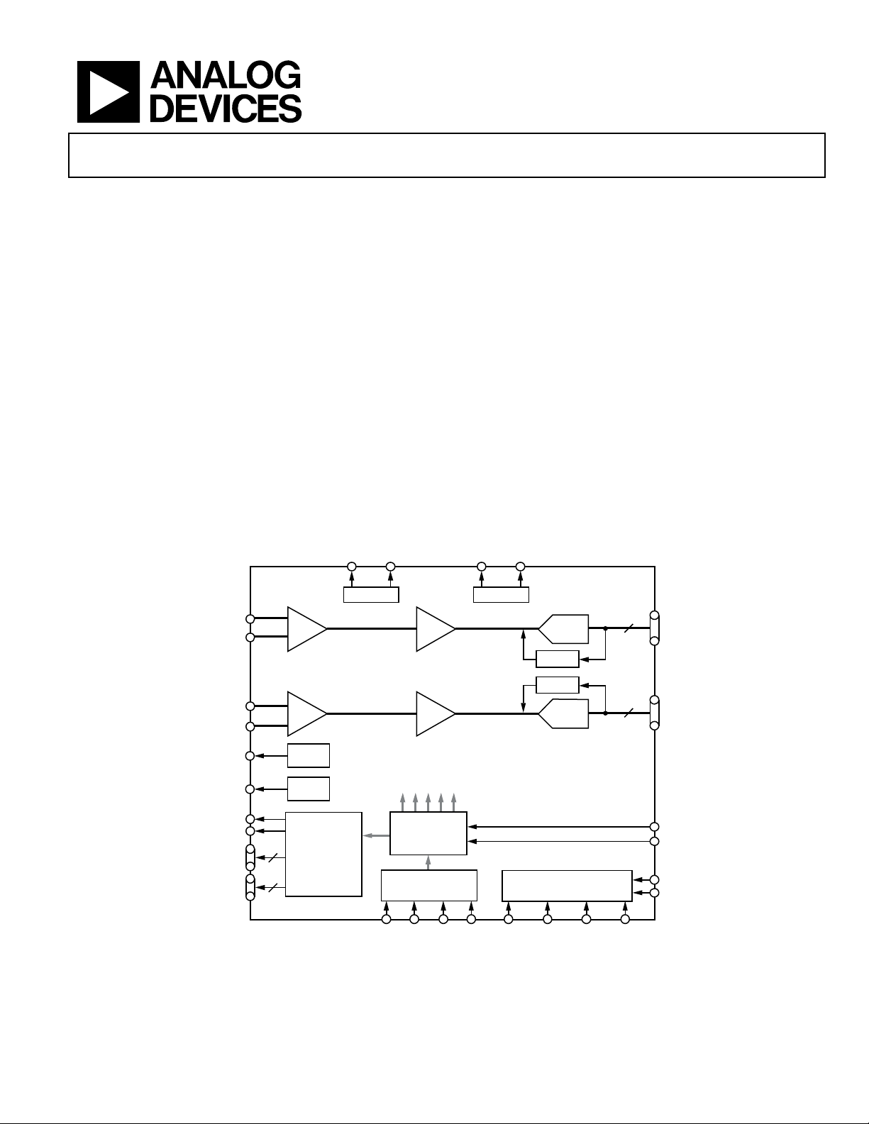
GENERAL DESCRIPTION
The AD9974 is a highly integrated, dual-channel, chargecoupled device (CCD) signal processor for high speed digital
video camera applications. Each channel is specified at pixel
rates of up to 65 MHz. The AD9974 consists of a complete
analog front end (AFE) with analog-to-digital conversion,
combined with a programmable timing driver. The Precision
Timi ng™ core allows adjustment of high speed clocks with
approximately 240 ps resolution at 65 MHz operation.
Each AFE includes black level clamping, CDS, VGA, and
a 65 MSPS, 14-bit ADC. The timing driver provides the high
speed CCD clock drivers for the RG_A, RG_B, H1_A to H4_A,
and H1_B to H4_B outputs. A 3-wire serial interface is used to
program each channel of the AD9974.
Available in a space-saving, 9 mm × 9 mm, CSP_BGA package,
the AD9974 is specified over an operating temperature range of
−25°C to +85°C.
AD9974
CCDINP_A
CCDINM_A
CCDINP_B
CCDINM_B
1.8V OUTP UT LDO A
1.8V OUTP UT LDO B
RG_A
RG_B
H1_A TO H4_
H1_B TO H4_B
4
4
CDS
CDS
HORIZONTAL
FUNCTIONAL BLOCK DIAGRAM
REFT_AREFB_
–3, 0, +3, +6dB
–3, 0, +3, +6dB
DRIVERS
VREF_A
VGA
VGA
INTERNAL CL OCKS
PRECISION
TIMING
CORE
SYNC
GENERATOR
HD_A VD_A HD_B VD_B
REFT_B REFB_B
6dB TO 42d B
6dB TO 42d B
Figure 1.
VREF_B
SL_A
CLAMP
CLAMP
INTERNAL
REGISTERS
SDATA_A
ADC
ADC
SL_B
14
14
SDATA_B
DOUT_A
DOUT_B
CLI_A
CLI_B
SCK_A
SCK_B
5955-001
Rev. A
Information furnished by Analog Devices is believed to be accurate and reliable. However, no
responsibility is assumed by Analog Devices for its use, nor for any infringements of patents or other
rights of third parties that may result from its use. Specifications subject to change without notice. No
license is granted by implication or otherwise under any patent or patent rights of Analog Devices.
Trademarks and registered trademarks are the property of their respective owners.
One Technology Way, P.O. Box 9106, Norwood, MA 02062-9106, U.S.A.
Tel: 781.329.4700 www.analog.com
Fax: 781.461.3113 ©2009 Analog Devices, Inc. All rights reserved.

AD9974
TABLE OF CONTENTS
Features .............................................................................................. 1
Applications ....................................................................................... 1
General Description ......................................................................... 1
Functional Block Diagram .............................................................. 1
Revision History ............................................................................... 2
Specifications ..................................................................................... 3
Channel-to-Channel Specifications ........................................... 3
Timing Specifications .................................................................. 4
Digital Specifications ................................................................... 5
Analog Specifications ................................................................... 6
Absolute Maximum Ratings ............................................................ 8
Thermal Characteristics .............................................................. 8
ESD Caution .................................................................................. 8
Pin Configuration and Function Descriptions ............................. 9
Typical Performance Characteristics ........................................... 11
Equivalent Input/Output Circuits ................................................ 12
Terminolog y .................................................................................... 13
Theory of Operation ...................................................................... 14
Programmable Timing Generation .............................................. 15
Precision Timing High Speed Timing Core ............................. 15
Horizontal Clamping and Blanking ......................................... 18
Complete Field—Combining H-Patterns ............................... 25
Mode Registers ........................................................................... 26
Horizontal Timing Sequence Example .................................... 28
Analog Front End Description and Operation ...................... 29
Applications Information .............................................................. 33
Recommended Power-Up Sequence ....................................... 33
Standby Mode Operation .......................................................... 36
CLI Frequency Change .............................................................. 36
Circuit Configuration ................................................................ 37
Grounding and Decoupling Recommendations .................... 37
3-Wire Serial Interface Timing ..................................................... 39
Layout of Internal Registers ...................................................... 40
Updating of Register Values ...................................................... 41
Complete Register Listing ............................................................. 42
Outline Dimensions ....................................................................... 50
Ordering Guide .......................................................................... 50
REVISION HISTORY
10/09—Revision A: Initial Version
Changes to Table 1 ............................................................................ 3
Changes to Table 3 ............................................................................ 4
Changes to Pin Function Descriptions Table ............................... 9
Changes to Figure 11 ...................................................................... 12
Changes to Individual HBLK Pattern Section ............................ 20
Changes to Table 14 ........................................................................ 25
Added Example Register Setting for Power-Up Section ........... 34
Added Additional Restrictions Section ....................................... 35
Changes to Table 2 .......................................................................... 36
Changes to 3 V System Compatibility Section ........................... 37
Changes to Grounding and Decoupling
Recommendations Section ............................................................ 37
Changes to Table 30 ........................................................................ 48
Changes to Table 31 ........................................................................ 49
Changes to Ordering Guide .......................................................... 50
Rev. A | Page 2 of 52
AD9974
SPECIFICATIONS
X = A = B, unless otherwise noted.
Table 1.
Parameter Min Typ Max Unit
TEMPERATURE RANGE
Operating −25 +85 °C
Storage −65 +150 °C
POWER SUPPLY VOLTAGE
AVDD_X (AFE, Timing Core) 1.6 1.8 2.0 V
RGVDD_X (RG_X Driver) 2.7 3.3 3.6 V
HVDD_X (H1_X to H4_X Drivers) 2.7 3.3 3.6 V
DVDD_X (All Other Digital) 1.6 1.8 2.0 V
DRVDD_X (Parallel Data Output Drivers) 1.6 3.0 3.6 V
IOVDD_X (I/O Supply Without the Use of LDO) 1.6 1.8 3.6 V
POWER SUPPLY CURRENTS—65 MHz OPERATION
AVDD_X (1.8 V) 55 mA
RGVDD_X (3.3 V, 20 pF RG Load) 5 mA
HVDD_X1 (3.3 V, 200 pF Total Load on H1 to H4) 40 mA
DVDD_X (1.8 V) 15 mA
DRVDD_X (3.0 V) 3 mA
IOVDD_X (1.8 V) 2 mA
POWER SUPPLY CURRENTS—STANDBY MODE OPERATION
Reference Standby 10 mA
Total Shutdown 0.5 mA
2
LDO
IOVDD_X (I/O Supply When Using LDO) 3.0 V
Output Voltage 1.85 V
Output Current 60 100 mA
CLOCK RATE (CLI) 8 65 MHz
1
The total power dissipated by the HVDD (or RGVDD) supply can be approximated as follows: Total HVDD Power = [C
Reducing the capacitive load and/or reducing the HVDD supply reduces the power dissipation. C
2
LDO should be used to supply only AVDD and DVDD.
is the total capacitance seen by all H-outputs.
LOAD
× HVDD × Pixel Frequency] × HVDD.
LOAD
CHANNEL-TO-CHANNEL SPECIFICATIONS
X = A = B, T
Table 2.
Parameter Min Typ Max Unit Test Conditions/Comments
LINEARITY MISMATCH
CROSSTALK ERROR CDS = 0 dB
Channel A to Channel B −82 dB Full-scale step applied to Channel A while measuring response on Channel B
Channel B to Channel A −82 dB Full-scale step applied to Channel B while measuring response on Channel A
1
See the section for further measurement explanation. Terminology
MIN
to T
, AVDD_X = DVDD_X = 1.8 V, f
MAX
1
<0.5 % Absolute value above 1⁄16 of maximum output code
= 65 MHz, typical timing specifications, unless otherwise noted.
CLI
Rev. A | Page 3 of 52

AD9974
TIMING SPECIFICATIONS
X = A = B, CL = 20 pF, AVDD_X = DVDD_X = 1.8 V, f
Table 3.
Parameter Min Typ Max Unit Comments
MASTER CLOCK (CLI) See Figure 17
CLI Clock Period (t
CLI High/Low Pulse Width (t
) 15.38 ns
CONV
) 6.9 7.7 8.9 ns
ADC
Delay from CLI Rising Edge to Internal Pixel Position 0 (t
AFE
SHP Rising Edge to SHD Rising Edge (tS1) 6.9 7.7 8.5 ns See Figure 21
AFE Pipeline Delay 16 Cycles See Figure 22
CLPOB Pulse Width (Programmable) (t
1
)
2 20 Pixels
COB
HD Pulse Width t
VD Pulse Width 1 HD period ns
SERIAL INTERFACE See Figure 52
Maximum SCK Frequency (f
) 40 MHz
SCLK
SL to SCK Setup Time (tLS) 10 ns
SCK to SL Hold Time (tLH) 10 ns
SDATA Valid to SCK Rising Edge Setup (tDS) 10 ns
SCK Rising Edge to SDATA Valid Hold (tDH) 10 ns
H-COUNTER RESET SPECIFICATIONS See Figure 49
HD Pulse Width t
VD Pulse Width 1 HD period ns
VD Falling Edge to HD Falling Edge(t
HD Falling Edge to CLI Rising Edge(t
) 0 VD period − t
VDHD
) 3 t
HDCLI
CLI Rising Edge to SHPLOC (Internal Sample Edge) (t
TIMING CORE SETTING RESTRICTIONS
Inhibited Region for SHP Edge Location (t
Inhibited Region for SHP or SHD with Respect to H-Clocks
(See Figure 21)
RETIME = 0, MASK = 0 (t
RETIME = 0, MASK = 1 (t
RETIME = 1, MASK = 0 (t
RETIME = 1, MASK = 1 (t
3, 4, 5, 6
) H × NEGLOC − 15 H × NEGLOC − 0 Edge location
SHDINH
) H × POSLOC − 15 H × POSLOC − 0 Edge location
SHDINH
) H × NEGLOC − 15 H × NEGLOC − 0 Edge location
SHPINH
) H × POSLOC − 15 H × POSLOC − 0 Edge location
SHPINH
) (See Figure 21)250 64/0 Edge location
SHPINH
Inhibited Region for DOUTPHASE Edge Location (t
(See Figure 21)
1
Minimum CLPOB pulse width is for functional operation only. Wider typical pulses are recommended to achieve good clamp performance.
2
Only applies to slave mode operation. The inhibited area for SHP is needed to meet the timing requirements for t
3
When 0x34[2:0] HxBLKRETIME bits are enabled, the inhibit region for SHD location changes to inhibit region for SHP location.
4
When sequence register 0x09[23:21] HBLK masking registers are set to 0, the H-edge reference becomes H × NEGLOC.
5
The H-clock signals that have SHP/SHD inhibit regions depend on the HCLK mode: Mode 1 = H1, Mode 2 = H1, H2, and Mode 3 = H1, H3.
6
These specifications apply when H1POL, H2POL, RGPOL, and HLPOL are all set to 1 (default setting).
= 65 MHz, unless otherwise noted.
CLI
) 5 ns
CLIDLY
ns
CONV
ns
CONV
) 3 t
CLISHP
DOUTINH
)
SHDLOC + 0 SHDLOC + 15 Edge location
ns
CONV
− 2 ns
CONV
− 2 ns
CONV
for proper H-counter reset operation.
CLISHP
Rev. A | Page 4 of 52
AD9974
DIGITAL SPECIFICATIONS
X = A = B, IOVDD_X = 1.6 V to 3.6 V, RGVDD_X = HVDD_X = 2.7 V to 3.6 V, CL = 20 pF, T
Table 4.
Parameter Min Typ Max Unit Test Conditions/Comments
LOGIC INPUTS
High Level Input Voltage (VIH) IOVDD − 0.6 V
Low Level Input Voltage (VIL) 0.6 V
High Level Input Current (IIH) 10 μA
Low Level Input Current (IIL) 10 μA
Input Capacitance (CIN) 10 pF
LOGIC OUTPUTS
High Level Output Voltage (VOH) IOVDD − 0.5 V IOH = 2 mA
Low Level Output Voltage (VOL) 0.5 V IOL = 2 mA
CLI INPUT (CLI_BIAS = 0)
High Level Input Voltage (V
Low Level Input Voltage (V
) IOVDD/2 + 0.5 V
IHCLI
) IOVDD/2 − 0.5 V
ILCLI
H-DRIVER OUTPUTS
High Level Output Voltage at Maximum Current (VOH) HVDD − 0.5 V
Low Level Output Voltage at Maximum Current 0.5 V
Maximum Output Current (Programmable) (VOL) 30 mA
Maximum Load Capacitance 100 pF
MIN
to T
, unless otherwise noted.
MAX
Rev. A | Page 5 of 52

AD9974
ANALOG SPECIFICATIONS
X = A = B, AVDD_X = 1.8 V, f
Table 5.
Parameter Min Typ Max Unit Test Conditions/Comments
CDS1
Allowable CCD Reset Transient 0.5 0.8 V
CDS Gain Accuracy
−3 dB CDS Gain −3.3 −2.8 −2.3
0 dB CDS Gain (Default) −0.7 −0.2 +0.3
3 dB CDS Gain 2.3 2.8 3.3
6 dB CDS Gain 4.9 5.4 5.9
Maximum Input Voltage VGA gain = 5.6 dB (Code 15, default value)
−3 dB CDS Gain 1.4 V p-p
0 dB CDS Gain (Default) 1.0 V p-p
3 dB CDS Gain 0.7 V p-p
6 dB CDS Gain 0.5 V p-p
Allowable OB Pixel Amplitude
0 dB CDS Gain (Default) −100 +200 mV
6 dB CDS Gain −50 +100 mV
VARIABLE GAIN AMPLIFIER (VGA_X)
Gain Control Resolution 1024 Steps
Gain Monotonicity Guaranteed
Low Gain Setting (VGA Code 15, Default) 6 dB
Maximum Gain Setting (VGA Code 1023) 42 dB
BLACK LEVEL CLAMP
Clamp Level Resolution 1024 Steps
Minimum Clamp Level (Code 0) 0 LSB Measured at ADC output
Maximum Clamp Level (Code 1023) 1023 LSB Measured at ADC output
ADC (CHN_A and CHN_B)
Resolution 14 Bits
Differential Nonlinearity (DNL) −1.0 ±0.5 +1.2 LSB
No Missing Codes Guaranteed
Integral Nonlinearity (INL) 5 15 LSB
Full-Scale Input Voltage 2.0 V
VOLTAGE REFERENCE
Reference Top Voltage (REFT_X) 1.4 V
Reference Bottom Voltage (REFB_X) 0.4 V
SYSTEM PERFORMANCE Specifications include entire signal chain
VGA Gain Accuracy 0 dB CDS gain (default)
Low Gain (Code 15) 5.1 5.6 6.1 dB Gain = (0.0359 × code) + 5.1 dB
Maximum Gain (Code 1023) 41.3 41.8 42.3 dB
Peak Nonlinearity, 500 mV Input Signal 0.1 0.4 % 12 dB total gain applied
Total Output Noise 2 LSB rms AC-grounded input, 6 dB gain applied
Power Supply Rejection (PSR) 48 dB Measured with step change on supply
1
Input signal characteristics are defined as shown in . Figure 2
= 65 MHz, typical timing specifications, T
CLI
MIN
to T
, unless otherwise noted.
MAX
Rev. A | Page 6 of 52

AD9974
800mV
MAXIMUM
500mV TYP
RESET TRANSIENT
200mV MAX
OPTICAL BLACK PIXEL
MAXIMUM INPUT LIMIT =
LESSER OF 2.2V
OR (AVDD + 0.3V )
+1.8V TYP (AVDD)
+1.3V TYP (AVDD – 0.5V)
DC RESTORE VO LTAGE
1V MAXIMUM INPUT
SIGNAL RANGE
(0dB CDS GAIN)
0V (AVSS)
MINIMUM INPUT LIMIT
(AVSS – 0.3V)
05957-002
Figure 2. Input Signal Characteristics
Rev. A | Page 7 of 52
AD9974
ABSOLUTE MAXIMUM RATINGS
Ratings apply to both Channel A and Channel B, unless
otherwise noted.
Table 6.
Parameter Rating
AVDD to AVSS −0.3 V to +2.2 V
DVDD to DVSS −0.3 V to +2.2 V
DRVDD to DRVSS −0.3 V to +3.9 V
IOVDD to DVSS −0.3 V to +3.9 V
HVDD to HVSS −0.3 V to +3.9 V
RGVDD to RGVSS −0.3 V to +3.9 V
Any VSS −0.3 V to +0.3 V
RG Output to RGVSS −0.3 V to RGVDD + 0.3 V
H1 to H4, HL Output to HVSS −0.3 V to HVDD + 0.3 V
SCK, SL, SDI to DVSS −0.3 V to IOVDD + 0.3 V
REFT, REFB, CCDINM, CCDINP to AVSS −0.2 V to AVDD + 0.2 V
Junction Temperature 150°C
Lead Temperature (10 sec) 350°C
Stresses above those listed under Absolute Maximum Ratings
may cause permanent damage to the device. This is a stress
rating only; functional operation of the device at these or any
other conditions above those indicated in the operational
section of this specification is not implied. Exposure to absolute
maximum rating conditions for extended periods may affect
device reliability.
THERMAL CHARACTERISTICS
θJA is measured using a 4-layer PCB with the exposed paddle
soldered to the board.
Table 7. Thermal Resistance
Package Type θJA Unit
100-Lead, 9 mm × 9 mm, CSP_BGA 38.3 °C/W
ESD CAUTION
Rev. A | Page 8 of 52
AD9974
PIN CONFIGURATION AND FUNCTION DESCRIPTIONS
AD9974
TOP VIEW
A1 CORNER
INDEX AREA
A
B
C
D
E
F
G
H
J
K
Figure 3. Pin Configuration
(Not to S cale)
2345678910
1
05955-003
Table 8. Pin Function Descriptions
Ball Location Mnemonic Type
1
Description
B2 SL_A DI 3-Wire Serial Load for Channel A.
C2 SDATA_A DI 3-Wire Serial Data for Channel A.
D2 SCK_A DI 3-Wire Serial Clock for Channel A.
C1 REFT_A AO Reference with Top Decoupling for Channel A. Decouple with 0.1 μF to AVSS_A.
D1 REFB_A AO Reference with Bottom Decoupling for Channel A. Decouple with 0.1 μF to AVSS_A.
A1 CCDINM_A AI Analog Input for Channel A Image Sensor Signal.
F4 H1_A DO CCD Horizontal Clock 1 for Channel A.
F3 H2_A DO CCD Horizontal Clock 2 for Channel A.
D4 H3_A DO CCD Horizontal Clock 3 for Channel A.
D3 H4_A DO CCD Horizontal Clock 4 for Channel A.
B4 RG_A DO CCD Reset Gate Clock for Channel A.
J2 DRVSS_A P Digital Driver Ground for Channel A.
K3 DRVDD_A P Digital Driver Supply for Channel A: 1.8 V or 3.0 V.
E3 HVSS_A P H1_A to H4_A Driver Ground for Channel A.
E4 HVDD_A P H1_A to H4_A Driver Supply for Channel A: 3.0 V.
C3 RGVSS_A P RG_A Driver Ground for Channel A.
C4 RGVDD_A P RG_A Driver Supply for Channel A: 3.0 V.
B3 IOVDD_A P
Digital I/O Supply: 1.8 V or 3.0 V (HD, VD, SL, SCK, SDATA) and LDO Input (3.0 V Only)
When LDO Is Used.
A4 CLI_A DI Master Clock Input for Channel A.
B1 AVSS_A P Analog Ground for Channel A.
A2 CCDINP_A AI Analog Input for Channel A Image Sensor Signal.
F2 DVSS_A P Digital Ground for Channel A.
F1 DVDD_A P Digital Supply for Channel A: 1.8 V.
E2 VD_A DI Vertical Sync Pulse for Channel A.
E1 HD_A DI Horizontal Sync Pulse for Channel A.
B8 SL_B DI 3-Wire Serial Load for Channel B.
C8 SDATA_B DI 3-Wire Serial Data for Channel B.
A5 LDO_OUT_A P 1.8 V LDO Output from Channel A.
A6 CCDINM_B AI Analog Input for Channel B Image Sensor Signal.
D8 SCK_B DI 3-Wire Serial Clock for Channel B.
C7 REFT_B AO Reference with Top Decoupling for Channel B. Decouple with 0.1 μF to AVSS_B.
D7 REFB_B AO Reference with Bottom Decoupling for Channel B. Decouple with 0.1 μF to AVSS_B.
A7 CCDINP_B AI Analog Input for Channel B Image Sensor Signal.
F10 H1_B DO CCD Horizontal Clock 1 for Channel B.
F9 H2_B DO CCD Horizontal Clock 2 for Channel B.
Rev. A | Page 9 of 52
AD9974
Ball Location Mnemonic Type
1
Description
D10 H3_B DO CCD Horizontal Clock 3 for Channel B.
D9 H4_B DO CCD Horizontal Clock 4 for Channel B.
B10 RG_B DO CCD Reset Gate Clock for Channel B.
J8 DRVSS_B P Digital Driver Ground for Channel B.
K9 DRVDD_B P Digital Driver Supply for Channel B: 1.8 V or 3.0 V.
E9 HVSS_B P H1_B to H4_B Driver Ground for Channel B.
E10 HVDD_B P H1_B to H4_B Driver Supply for Channel B: 3.0 V.
C9 RGVSS_B P RG_B Driver Ground for Channel B.
C10 RGVDD_B P RG_B Driver Supply for Channel B: 3.0 V.
B9 IOVDD_B P
Digital I/O Supply: 1.8 V or 3.0 V (HD, VD, SL, SCK, SDATA) and LDO Input (3.0 V Only)
When LDO Is Used.
A10 LDO_OUT_B P 1.8 V LDO Output from Channel B.
B7 AVSS_B P Analog Ground for Channel B.
A8 AVDD_B P Analog Supply for Channel B: 1.8 V.
F8 DVSS_B P Digital Ground for Channel B.
F7 DVDD_B P Digital Supply for Channel B: 1.8 V.
E8 VD_B DI Vertical Sync Pulse for Channel B.
E7 HD_B DI Horizontal Sync Pulse for Channel B.
A3 AVDD_A P Analog Supply for Channel A: 1.8 V.
G1 D0_A DO Data Outputs Channel A.
H1 D1_A DO Data Outputs Channel A.
J1 D2_A DO Data Outputs Channel A.
K1 D3_A DO Data Outputs Channel A.
G2 D4_A DO Data Outputs Channel A.
H2 D5_A DO Data Outputs Channel A.
K2 D6_A DO Data Outputs Channel A.
G3 D7_A DO Data Outputs Channel A.
H3 D8_A DO Data Outputs Channel A.
J3 D9_A DO Data Outputs Channel A.
K4 D10_A DO Data Outputs Channel A.
J4 D11_A DO Data Outputs Channel A.
H4 D12_A DO Data Outputs Channel A.
G4 D13_A DO Data Outputs Channel A.
B5, C5, D5, E5, F5, G5, H5,
GND P Ground Connection.
J5, K5, B6, C6, D6, E6, F6,
G6, H6, J6, K6
A9 CLI_B DI Master Clock Input for Channel B.
G7 D0_B DO Data Outputs Channel B.
H7 D1_B DO Data Outputs Channel B.
J7 D2_B DO Data Outputs Channel B.
K7 D3_B DO Data Outputs Channel B.
G8 D4_B DO Data Outputs Channel B.
H8 D5_B DO Data Outputs Channel B.
K8 D6_B DO Data Outputs Channel B.
G9 D7_B DO Data Outputs Channel B.
H9 D8_B DO Data Outputs Channel B.
J9 D9_B DO Data Outputs Channel B.
K10 D10_B DO Data Outputs Channel B.
J10 D11_B DO Data Outputs Channel B.
H10 D12_B DO Data Outputs Channel B.
G10 D13_B DO Data Outputs Channel B.
1
AI = analog input, AO = analog output, DI = digital input, DO = digital output, P = power.
Rev. A | Page 10 of 52
AD9974
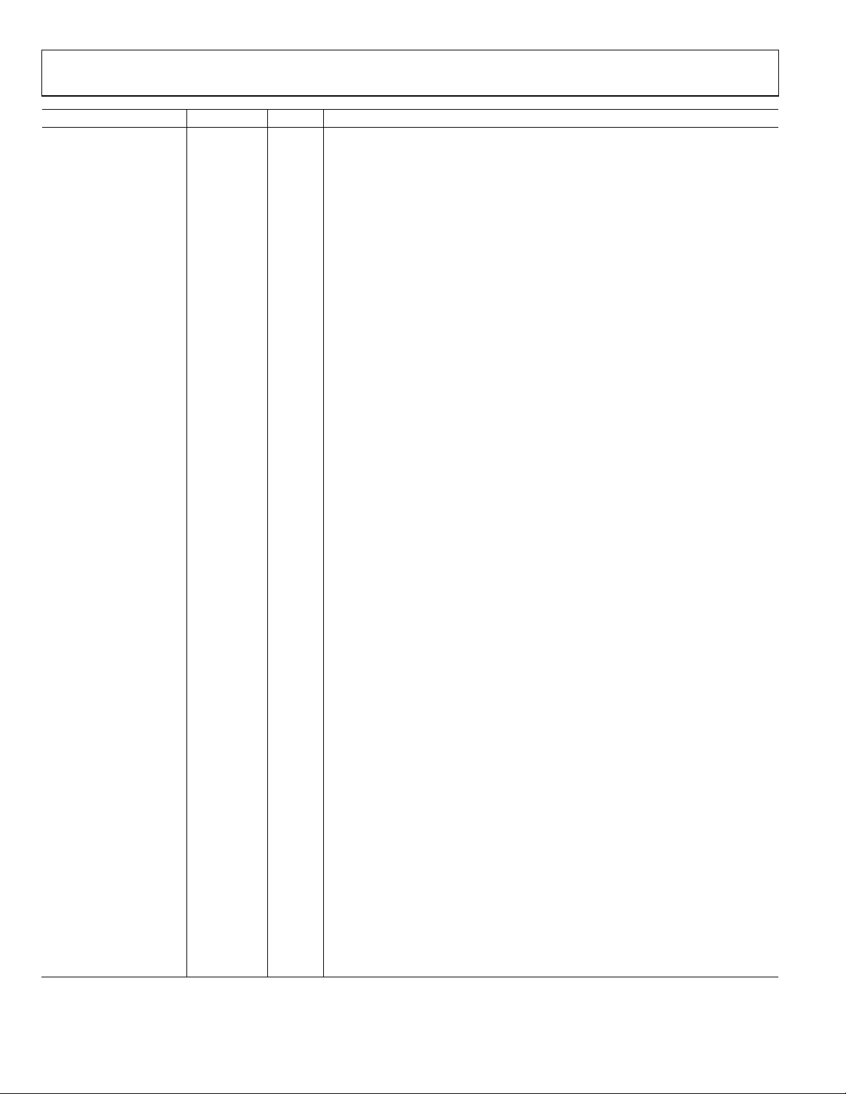
TYPICAL PERFORMANCE CHARACTERISTICS
250
200
150
100
POWER (mW)
50
0
20 25 30 35 40 45 50 55 60 65
TOTAL POWER
3.3V SUPPLIES
1.8V SUPPLIES
SAMPLE RATE (MHz)
Figure 4. Power vs. Sample Rate
05955-005
10
8
6
4
2
LSB
0
–2
–4
–6
–8
0
2k 4k 6k 8k 10k 12k 14k 16k
ADC OUTPUT CODE
05955-008
Figure 7. Integral Nonlinearity
180
160
140
120
100
80
60
RMS OUTPUT NOISE (LSB)
40
20
0
0 5 10 15 20 25 30 35 40 45
VGA GAIN (dB)
Figure 5. RMS Output Noise vs. VGA Gain
1.0
0.8
0.6
0.4
0.2
0
LSB
–0.2
–0.4
–0.6
–0.8
–1.0
0
2k 4k 6k 8k 10k 12k 14k 16k
ADC OUTPUT CODE
Figure 6. Differential Nonlinearity
1.0
0.8
0.6
0.4
0.2
0
–0.2
INL MISMATCH (%)
–0.4
–0.6
–0.8
–1.0
1k
3k 5k 7k 9k 11k 13k 15k
05955-006
ADC OUTPUT CODE
05955-009
Figure 8. Linearity Mismatch vs. ADC Output Code
05955-007
Rev. A | Page 11 of 52
AD9974
A
V
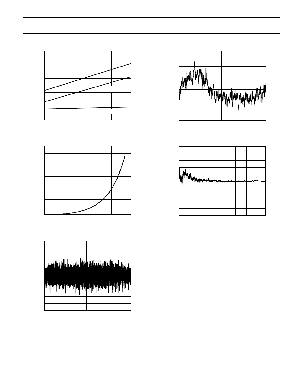
EQUIVALENT INPUT/OUTPUT CIRCUITS
DD
R
AVSS AVSS
Figure 9. CCDIN Input
IOVDD
330Ω
IOVDD
CLI
05955-010
330Ω
AVSS
100kΩ
+
05955-011
Figure 11. CLI Input, Register 0x15[0] = 1 Enables the Bias Circuit
HVDD OR RGVDD
DATA
ENABLE
OUTPUT
DVSS
Figure 10. Digital Inputs
05955-012
HVSS OR RGVSS
5955-013
Figure 12. H1 to H4 and RG Outputs
Rev. A | Page 12 of 52
AD9974
TERMINOLOGY
Differential Nonlinearity (DNL)
An ideal ADC exhibits code transitions that are exactly 1 LSB
apart. DNL is the deviation from this ideal value. Therefore,
every code must have a finite width. No missing codes guaranteed
to 14-bit resolution indicates that all 16,384 codes, each for its
respective input, must be present over all operating conditions.
Peak Nonlinearity
Peak nonlinearity, a full signal chain specification, refers to the
peak deviation of the output of the AD9974 from a true straight
line. The point used as zero scale occurs 0.5 LSB before the first
code transition. Positive full scale is defined as a level 1 LSB
and 0.5 LSB beyond the last code transition. The deviation is
measured from the middle of each particular output code to the
true straight line. The error is then expressed as a percentage
of the 2 V ADC full-scale signal. The input signal is always
appropriately gained up to fill the ADC full-scale range.
Tot a l O ut p ut Noi se
The rms output noise is measured using histogram techniques.
The standard deviation of the ADC output codes is calculated
in LSB and represents the rms noise level of the total signal
chain at the specified gain setting. The output noise can be
converted to an equivalent voltage using the relationship
1 LSB = (ADC Full Scale/2
where n is the bit resolution of the ADC. For the AD9974,
1 LSB is approximately 122.0 μV.
Linearity Mismatch
The linearity mismatch is calculated by taking the difference in
INL of the two channels at Input X, and then expressing the
difference as a percentage of the output code at X. The values
given in Tab le 2 are obtained over the range of 1⁄16 and
maximum of the output code. The general trend is for the
linearity mismatch to decrease as the output approaches the
maximum code, as shown in Figure 8.
n
Codes)
MAX
OUTPUT CODE (LSB)
OUTPUT (X)
MAX/16
INL A(X)
INL B(X)
0
0
XFS
INPUT VOLTAGE
Figure 13. Linearity Mismatch Definition
CHANNEL B
IDEAL
CHANNEL A
Power Supply Rejection (PSR)
The PSR is measured with a step change applied to the supply
pins. The PSR specification is calculated from the change in the
data outputs for a given step change in the supply voltage.
Crosstalk
The crosstalk is measured while applying a full-scale step to
one channel and measuring the interference on the opposite
channel.
)(
LSBceInterferen
⎛
⎜
×=
Crosstalk
log20)dB(
⎜
⎝
384,16
⎞
⎟
⎟
⎠
5955-004
MismatchLinearity
=
(%)
−
XBINLXAINL
)()(
XCodeOutput
)(
Rev. A | Page 13 of 52
AD9974
THEORY OF OPERATION
V DRIVER
H1_A TO H4_A, RG_A
H1_B TO H4_B, RG_B
CCDINP_A
CCDINM_A
CCD
CCDINP_B
CCDINM_B
V1 > Vx, VSG 1 > VS Gx, SUBCK
AD9974
INTEGRATED
AFE + TD
SERIAL
INTERFACE
DOUT_A
DOUT_B
HD_A, VD_A,
HD_B, VD_B
CLI_A, CLI _B
DIGITAL IMAGE
PROCESSING
ASIC
05955-014
Figure 14. Typical Application
Figure 14 shows the typical system block diagram for the AD9974.
The charge-coupled device (CCD) output is processed by the
analog front-end (AFE) circuitry of the AD9974, consisting of a
CDS, VGA, black level clamp, and ADC. The digitized pixel
information is sent to the digital image processor chip, which
performs the postprocessing and compression. To operate the
CCD, all CCD timing parameters are programmed into the
AD9974 from the system ASIC through the 3-wire serial
interface. From the system master clock, CLI_X, which is provided
by the image processor or external crystal, the AD9974 generates
the horizontal clocks of the CCD and all internal AFE clocks.
MAX VD LENG TH IS 8192 LINES
All AD9974 clocks are synchronized with VD and HD inputs.
All of the AD9974 horizontal pulses (CLPOB, PBLK, and
HBLK) are programmed and generated internally.
The H-drivers for H1 to H4 and RG are included in the
AD9974, allowing these clocks to be directly connected to the
CCD. An H-driver voltage of 3 V is supported in the AD9974.
Figure 15 and Figure 16 show the maximum horizontal and
vertical counter dimensions for the AD9974. All internal horizontal
and vertical clocking is controlled by these counters, which specify
line and pixel locations. Maximum HD length is 8191 pixels per
line, and maximum VD length is 8191 lines per field.
MAXIMUM COUNTE R DIM ENS I O NS
13-BIT HORIZONTAL = 8192 PIXELS MAX
13-BIT VERTICAL = 8192 L INES MAX
5955-015
Figure 15. Vertical and Horizontal Counters
CLI
VD
HD
MAX HD LENGTH IS 8192 PIXELS
Figure 16. Maximum VD/HD Dimensions
Rev. A | Page 14 of 52
05955-016
AD9974
S
PROGRAMMABLE TIMING GENERATION
PRECISION TIMING HIGH SPEED TIMING CORE
The AD9974 generates flexible high speed timing signals using
the Precision Timing core. This core, composed of the Reset
Gate RG, Horizontal Driver H1 to Horizontal Driver H4, and
SHP/SHD sample clocks, is the foundation for generating the
timing for both the CCD and the AFE. A unique architecture
makes it routine for the system designer to optimize image
quality by providing precise control over the horizontal CCD
readout and the AFE correlated double sampling.
Timing Resolution
The Precision Timing core uses a master clock input (CLI_X)
as a reference. This clock input should be the same as the CCD
pixel clock frequency. Figure 17 illustrates how the internal timing
core divides the master clock period into 64 steps or edge positions;
therefore, the edge resolution of the Precision Timing core is
(t
/64). For more information on using the CLI input, refer to
CLI
the Applications Information section.
POSITION
P[0] P[64] = P[0]P[16] P[32] P[48]
Using a 65 MHz CLI frequency, the edge resolution of the
Precision Timing core is approximately 240 ps. If a 1× system
clock is not available, it is possible to use a 2× reference clock
by programming the CLIDIVIDE register (Address 0x0D). The
AD9974 then internally divides the CLI frequency by 2.
High Speed Clock Programmability
Figure 18 shows when the high speed clocks, RG, H1 to H4,
SHP, and SHD, are generated. The RG pulse has programmable
rising and falling edges and can be inverted using the polarity
control. The H1 and H2 horizontal clocks have separate programmable rising and falling edges, as well as separate polarity control.
The AD9974 provides additional HCLK-mode programmability,
as described in Ta bl e 9 .
The edge location registers are each six bits wide, allowing the
selection of all 64 edge locations. Figure 21 shows the default
timing locations for all of the high speed clock signals.
CLI
t
CLIDLY
1 PIXEL
PERIOD
NOTES
1. THE PIXEL CLOCK PERIOD IS DIVIDED INTO 64 POSITIONS, PROVIDING FINE EDGE RESOLUTION FOR HIGH SPEED CLOCKS.
2. THERE IS A F I XED DELAY FROM THE CLI INPUT TO THE INTERNAL PIXEL PERIOD POSITION (
t
CLIDLY
).
5955-017
Figure 17. High Speed Clock Resolution from CLI Master Clock Input
1
CCD
IGNAL
34
RG
56
H1, H3
H2, H4
PROGRAMMABLE CLOCK POSI T IONS:
1
SHP SAMPLE LOCATION.
2
SHD SAMPLE LO CAT I O N.
3
RG RISING EDGE.
4
RG FALLING EDGE.
5
H1 RISING EDGE.
6
H1 FALLING EDGE.
Figure 18. High Speed Clock Programmable Locations (HCLK Mode 1)
2
05955-018
Rev. A | Page 15 of 52
AD9974
12
H1, H3
43
H2, H4
H1 TO H4 P R OGRAMM A B LE LO CATI ONS:
1
H1 RISING EDGE.
2
H1 FALLING EDGE.
3
H2 RISING EDGE.
4
H2 FALLING EDGE.
5955-019
Figure 19. HCLK Mode 2 Operation
12
H1
H2
3
H3
H4
H1 TO H4 PROGRAMMABLE LOCATIONS:
1
H1 RISIN G EDGE .
2
H1 FALLING EDGE.
3
H3 RISIN G EDGE .
4
H3 FALLING EDGE.
4
05955-020
Figure 20. HCLK Mode 3 Operation
P[0]
P[32]P[16] P[48]POSITION
P[64] = P[0]
CLI
RGr[0] RGf[16]
RG
H1r[0] H1f[32]
H1
H2
t
CCD
SIGNAL
SHPLOC[32]
SHP
SHDLOC[0]
SHD
t
DOUTPHASEP
NOTES
1. ALL SIGNAL EDGES ARE FULLY PROGRAMMABLE TO ANY OF THE 64 POSITIONS WITHIN ONE PIXEL PERIOD.
TYPICAL P OSITI ONS FOR EACH SIGNAL ARE SHO WN. HCLK MODE 1 IS SHOWN.
2. CERTAIN POSITIONS SHOULD BE AVOIDED FO R EACH SIGNAL, S HOWN ABOVE AS INHIBIT REGIONS.
3. IF A SETTING I N THE INHIBIT REGION IS USED, AN UNSTABLE PIXEL S HIFT CAN OCCUR IN THE HBLK LOCATION OR AF E P IPELINE.
DOUTINH
DATAPHASEP[32]
S1
t
SHPINH
t
SHDINH
05955-021
Figure 21. High Speed Timing Default Locations
Rev. A | Page 16 of 52

AD9974
Table 9. HCLK Modes, Selected by HCLKMODE Register (Address 0x23[7:5])
HCLK Mode Register Value Description
Mode 1 001 H1 edges are programmable, with H3 = H1 and H2 = H4 = inverse of H1.
Mode 2 010
Mode 3 100
Invalid Selection 000, 011, 101, 110, 111 Invalid register settings.
Table 10. H1, H2, RGCONTROL, DRVCONTROL, and SAMPCONTROL Register Parameters
Parameter Length (Bits) Range Description
Polarity 1 High/low
Positive Edge 6 0 to 63 edge location Positive edge location for H1/H3 and RG.
Negative Edge 6 0 to 63 edge location Negative edge location for H1/H3 and RG.
Sample Location 6 0 to 63 sample location Sampling location for SHP and SHD.
Drive Control 3 0 to 7 current steps Drive current for H1 to H4 and RG outputs, 0 to 7 steps of 4.3 mA each.
CLI
t
CLIDLY
CCDIN
NN+2N+1
N+3
N+4
H1 edges are programmable, with H3 = H1.
H2 edges are programmable, with H4 = H2.
H1 edges are programmable, with H2 = inverse of H1.
H3 edges are programmable, with H4 = inverse of H3.
Polarity control for H1/H3 and RG.
0 = no inversion.
1 = inversion.
N+13N+12N+11N+10N+9N+8N+7N+6N+5
N+14
N+16 N+17N+15
SHD
(INTERNAL)
ADC OUT
(INTERNAL)
DOUTPHASE
CLK
DOUT
NOTES
1. EXAMPLE SHOWN FOR SHDLO C = 0.
2. HIGHER VALUES OF SHD AND/ OR DOUTPHASE W ILL SHIFT DOUT TRANSITIO N TO THE RIGHT, WITH RESPECT TO CLI LOCATIO N.
SAMPLE PIXEL N
t
DOUTINH
N–14 N–4N–5N–6N–7N–8N–9N–10N–11N–12N–13 N–3 N–2 N–1 N N+1N–15N–16N–17
PIPELINE LATENCY = 16 CYCLES
N–14 N–4N–5N–6N–7N–8N–9N–10N–11N–12N–13 N–3 N–2 N–1 N N+1N–15N–16N–17
Figure 22. Pipeline Delay of AFE Data Outputs
H-Driver and RG Outputs Digital Data Outputs
In addition to the programmable timing positions, the AD9974
features on-chip output drivers for the RG and H1 to H4 outputs.
These drivers are powerful enough to drive the CCD inputs
directly. The H-driver and RG-driver current can be adjusted
for optimum rise/fall time into a particular load by using the
drive strength control registers (Address 0x35). Use the register
to adjust the drive strength in 4.3 mA increments. The minimum
setting of 0 is equal to off or three-state, and the maximum setting
of 7 is equal to 30.1 mA.
For maximum system flexibility, the AD9974 uses the
DOUTPHASE registers (Address 0x37[11:0]) to select the
location for the start of each new pixel data value. Any edge
location from 0 to 63 can be programmed. These registers
determine the start location of the data output and the DCLK
rising edge with respect to the master clock input, CLI_X.
The pipeline delay through the AD9974 is shown in Figure 22.
After the CCD input is sampled by SHD, there is a 16-cycle
delay until the data is available.
5955-022
Rev. A | Page 17 of 52

AD9974
C
HORIZONTAL CLAMPING AND BLANKING
The horizontal clamping and blanking pulses of the AD9974 are
fully programmable to suit a variety of applications. Individual
control is provided for CLPOB, PBLK, and HBLK during the
different regions of each field. This allows the dark pixel clamping
and blanking patterns to be changed at each stage of the readout
to accommodate different image transfer timing and high speed
line shifts.
Individual CLPOB and PBLK Patterns
The AFE horizontal timing consists of CLPOB and PBLK, as
shown in Figure 23. These two signals are programmed independently using the registers in Tab le 1 1 . The start polarity for
the CLPOB or PBLK signal is CLPOB_POL (PBLK_POL), and the
first and second toggle positions of the pulse are CLPOB_TOG1
(PBLK_TOG1) and CLPOB_TOG2 (PBLK_TOG2). Both signals
are active low and need to be programmed accordingly.
Two separate patterns for CLPOB and PBLK can be programmed
for each H-pattern, CLPOB0, CLPOB1, PBLK0, and PBLK1.
The CLPOB_PAT and PBLK_PAT field registers select which
of the two patterns is used in each field.
Figure 34 shows how the sequence change positions divide the
readout field into different regions. By assigning a different
H-pattern to each region, the CLPOB and PBLK signals can
change with each change in the vertical timing.
CLPOB and PBLK Masking Area
Additionally, the AD9974 allows the CLPOB and PBLK signals
to be disabled during certain lines in the field without changing
any of the existing pattern settings. There are three sets of start
and end registers for both CLPOB and PBLK that allow the
creation of up to three masking areas for each signal.
For example, to use the CLPOB masking, program the
CLPOBMASKSTART and CLPOBMASKEND registers to
specify the starting and ending lines in the field where the CLPOB
patterns are to be ignored. Figure 24 illustrates this feature.
The masking registers are not specific to a certain H-pattern;
they are always active for any existing field of timing. To disable
the CLPOB and PBLK masking feature, set these registers to the
maximum value of 0x1FFF.
Note that to disable CLPOB and PBLK masking during
power-up, it is recommended that CLPOBMASKSTART
(PBLKMASKSTART) be set to 8191 and CLPOBMASKEND
(PBLKMASKEND) be set to 0. This prevents any accidental
masking caused by different register update events.
HD
CLPOB
1
PBLK
PROGRAMMABLE SETTI NGS :
1
START POLARITY (CLAM P AND BLANK REGION ARE ACTIVE LO W).
2
FIRST TOGGLE POSITION.
3
SECOND TOGGLE POSITION.
ACTIVE
32
Figure 23. Clamp and Preblank Pulse Placement
ACTIVE
05955-023
VD
HD
LPOB
NO CLPOB SI GNAL
FOR LINE S 6 TO 8
0 1 2 597 598
CLPOBMASKSTART1 = 6 CL P OBMASKEND1 = 8
Figure 24. CLPOB Masking Example
CLPOBMASKSTART2 = CLPOBMASKEND2 = 600
NO CLPOB SI GNAL
FOR LINE 600
05957-024
Rev. A | Page 18 of 52

AD9974
Table 11. CLPOB and PBLK Pattern Registers
Parameter Length (Bits) Range Description
CLPOB0_TOG1 13 0 to 8191 pixel location First CLPOB0 toggle position within the line for each V-sequence.
CLPOB0_TOG2 13 0 to 8191 pixel location Second CLPOB0 toggle position within the line for each V-sequence.
CLPOB1_TOG1 13 0 to 8191 pixel location First CLPOB1 toggle position within the line for each V-sequence.
CLPOB1_TOG2 13 0 to 8191 pixel location Second CLPOB1 toggle position within the line for each V-sequence.
CLPOB_POL 9 High/low Starting polarity of CLPOB for each V-sequence [8:0] (in field registers).
CLPOB_PAT 9 0 to 9 settings CLPOB pattern selection for each V-sequence [8:0] (in field registers).
CLPOBMASKSTART 13 0 to 8191 pixel location CLPOB mask start position: three values available (in field registers).
CLPOBMASKEND 13 0 to 8191 pixel location CLPOB mask end position: three values available (in field registers).
PBLK0_TOG1 13 0 to 8191 pixel location First PBLK0 toggle position within the line for each V-sequence.
PBLK0_TOG2 13 0 to 8191 pixel location Second PBLK0 toggle position within the line for each V-sequence.
PBLK1_TOG1 13 0 to 8191 pixel location First PBLK1 toggle position within the line for each V-sequence.
PBLK1_TOG2 13 0 to 8191 pixel location Second toggle position within the line for each V-sequence.
PBLK_POL 9 High/low Starting polarity of PBLK for each V-sequence [8:0] (in field registers).
PBLK_PAT 9 0 to 9 settings PBLK pattern selection for each V-sequence [8:0] (in field registers).
PBLKMASKSTART 13 0 to 8191 pixel location PBLK mask start position: three values available (in field registers).
PBLKMASKEND 13 0 to 8191 pixel location PBLK mask end position: three values available (in field registers).
HD
HBLKTOGE1 HBLKTOGE2
HBLK
BLANK BLANK
BASIC HBLK PULSE IS GENERATED USING HBLKTOGE1 AND HBLKTOGE2 REGISTERS ( HBLKALT = 0).
Figure 25. Typical Horizontal Blanking Pulse Placement (HBLKMODE = 0)
05955-025
HD
HBLK
H1/H3
THE POLARITY OF H1/H3 DURING BLANKI NG IS PROG RAM M ABLE
(H2/H4 POLARITY IS SEPARATELY PROGRAMMABLE)
H1/H3
H2/H4
Figure 26. HBLK Masking Control
05955-026
Rev. A | Page 19 of 52

AD9974
Individual HBLK Patterns
The HBLK programmable timing shown in Figure 25 is similar
to CLPOB and PBLK; however, there is no start polarity control.
Only the toggle positions designate the start and the stop positions
of the blanking period. Additionally, as shown in Figure 26, there
is a polarity control, HBLKMASK, for H1/H3 and H2/H4 that
designates the polarity of the horizontal clock signals during the
blanking period. Setting HBLKMASK_H1 low sets H1 = H3 =
low and HBLKMASK_H2 high sets H2 = H4 = high during the
blanking. As with the CLPOB and PBLK signals, HBLK registers
are available in each H-pattern group, allowing unique blanking
signals to be used with different vertical timing sequences.
The AD9974 supports three modes of HBLK operation. HBLK
Mode 0 supports basic operation and provides some support for
special HBLK patterns. HBLK Mode 1 supports pixel mixing
HBLK operation. HBLK Mode 2 supports advanced HBLK operation. The following sections describe each mode. Register
parameters are detailed in Tab l e 1 2 .
HBLKTOGE2
HBLKTOGE1
HBLKTOGE3
HBLKTOGE4
HBLK Mode 0 Operation
There are six toggle positions available for HBLK. Normally,
only two of the toggle positions are used to generate the standard
HBLK interval. However, the additional toggle positions can be
used to generate special HBLK patterns, as shown in Figure 27.
The pattern in this example uses all six toggle positions to generate
two extra groups of pulses during the HBLK interval. By changing
the toggle positions, different patterns are created.
Separate toggle positions are available for even and odd lines.
If alternation is not needed, load the same values into the registers
for even (HBLKTOGE) and odd (HBLKTOGO) lines.
HBLKTOGE6
HBLKTOGE5
HBLK
H1/H3
H2/H4
SPECIAL H-BL ANK P ATTERN IS CREATED USING MUL TIPLE HBLK TOGGLE POSITIONS (HBL KALT = 0).
Figure 27. Generating Special HBLK Patterns
05955-027
Table 12. HBLK Pattern Registers
Register Length (Bits) Range Description
HBLK_MODE 2 0 to 2 HBLK modes Enables different HBLK toggle position operations.
0 = normal mode. Six toggle positions available for even and odd lines.
If even/odd alternation is not needed, set toggles for even/odd the same.
1 = pixel mixing mode. In addition to six toggle positions, the HBLKSTART,
HBLKEND, HBLKLEN, and HBLKREP registers can be used to generate HBLK
patterns. If even/odd alternation is not needed, set toggles for even/odd
the same.
2 = advanced HBLK mode. Divides HBLK interval into six different repeat
areas. Uses HBLKSTARTA/B/C and RA*H*REPA/B/C registers.
3 = test mode only. Do not access.
HBLKSTART 13 0 to 8191 pixel location Start location for HBLK in HBLK Mode 1 and HBLK Mode 2.
HBLKEND 13 0 to 8191 pixel location End location for HBLK in HBLK Mode 1 and HBLK Mode 2.
HBLKLEN 13 0 to 8191 pixels HBLK length in HBLK Mode 1 and HBLK Mode 2.
HBLKREP 13 0 to 8191 repetitions Number of HBLK repetitions in HBLK Mode 1 and HBLK Mode 2.
HBLKMASK_H1 1 High/low Masking polarity for H1 and H3 during HBLK.
HBLKMASK_H2 1 High/low Masking polarity for H2 and H4 during HBLK.
Rev. A | Page 20 of 52

AD9974
Register Length (Bits) Range Description
HBLKTOGO1 13 0 to 8191 pixel location First HBLK toggle position for odd lines in HBLK Mode 0 and HBLK Mode 1.
HBLKTOGO2 13 0 to 8191 pixel location Second HBLK toggle position for odd lines in HBLK Mode 0 and HBLK Mode 1.
HBLKTOGO3 13 0 to 8191 pixel location Third HBLK toggle position for odd lines in HBLK Mode 0 and HBLK Mode 1.
HBLKTOGO4 13 0 to 8191 pixel location Fourth HBLK toggle position for odd lines in HBLK Mode 0 and HBLK Mode 1.
HBLKTOGO5 13 0 to 8191 pixel location Fifth HBLK toggle position for odd lines in HBLK Mode 0 and HBLK Mode 1.
HBLKTOGO6 13 0 to 8191 pixel location Sixth HBLK toggle position for odd lines in HBLK Mode 0 and HBLK Mode 1.
HBLKTOGE1 13 0 to 8191 pixel location First HBLK toggle position for even lines in HBLK Mode 0 and HBLK Mode 1.
HBLKTOGE2 13 0 to 8191 pixel location Second HBLK toggle position for even lines in HBLK Mode 0 and HBLK Mode 1.
HBLKTOGE3 13 0 to 8191 pixel location Third HBLK toggle position for even lines in HBLK Mode 0 and HBLK Mode 1.
HBLKTOGE4 13 0 to 8191 pixel location Fourth HBLK toggle position for even lines in HBLK Mode 0 and HBLK Mode 1.
HBLKTOGE5 13 0 to 8191 pixel location Fifth HBLK toggle position for even lines in HBLK Mode 0 and HBLK Mode 1.
HBLKTOGE6 13 0 to 8191 pixel location Sixth HBLK toggle position for even lines in HBLK Mode 0 and HBLK Mode 1.
RA0H1REPA/B/C 12
[3:0] RA0H1REPA. Number of H1 pulses following HBLKSTARTA.
[7:4] RA0H1REPB. Number of H1 pulses following HBLKSTARTB.
[11:8] RA0H1REPC. Number of H1 pulses following HBLKSTARTC.
RA1H1REPA/B/C 12 0 to 15 HCLK pulses HBLK Repeat Area 1. Number of H1 repetitions for HBLKSTARTA/B/C.
RA2H1REPA/B/C 12 0 to 15 HCLK pulses HBLK Repeat Area 2. Number of H1 repetitions for HBLKSTARTA/B/C.
RA3H1REPA/B/C 12 0 to 15 HCLK pulses HBLK Repeat Area 3. Number of H1 repetitions for HBLKSTARTA/B/C.
RA4H1REPA/B/C 12 0 to 15 HCLK pulses HBLK Repeat Area 4. Number of H1 repetitions for HBLKSTARTA/B/C.
RA5H1REPA/B/C 12 0 to 15 HCLK pulses HBLK Repeat Area 5. Number of H1 repetitions for HBLKSTARTA/B/C.
RA0H2REPA/B/C 12
[3:0] RA0H2REPA. Number of H2 pulses following HBLKSTARTA.
[7:4] RA0H2REPB. Number of H2 pulses following HBLKSTARTB.
[11:8] RA0H2REPC. Number of H2 pulses following HBLKSTARTC.
RA1H2REPA/B/C 12 0 to 15 HCLK pulses HBLK Repeat Area 1. Number of H2 repetitions for HBLKSTARTA/B/C.
RA2H2REPA/B/C 12 0 to 15 HCLK pulses HBLK Repeat Area 2. Number of H2 repetitions for HBLKSTARTA/B/C.
RA3H2REPA/B/C 12 0 to 15 HCLK pulses HBLK Repeat Area 3. Number of H2 repetitions for HBLKSTARTA/B/C.
RA4H2REPA/B/C 12 0 to 15 HCLK pulses HBLK Repeat Area 4. Number of H2 repetitions for HBLKSTARTA/B/C.
RA5H2REPA/B/C 12 0 to 15 HCLK pulses HBLK Repeat Area 5. Number of H2 repetitions for HBLKSTARTA/B/C.
HBLKSTARTA 13 0 to 8191 pixel location HBLK Repeat Area Start Position A for HBLK Mode 2.
HBLKSTARTB 13 0 to 8191 pixel location HBLK Repeat Area Start Position B for HBLK Mode 2.
HBLKSTARTC 13 0 to 8191 pixel location HBLK Repeat Area Start Position C for HBLK Mode 2.
HBLKALT_PAT1 3 0 to 5 even repeat area
HBLKALT_PAT2 3 0 to 5 even repeat area HBLK Mode 2, Odd Field Repeat Area 1 pattern.
HBLKALT_PAT3 3 0 to 5 even repeat area HBLK Mode 2, Odd Field Repeat Area 2 pattern.
HBLKALT_PAT4 3 0 to 5 even repeat area HBLK Mode 2, Odd Field Repeat Area 3 pattern.
HBLKALT_PAT5 3 0 to 5 even repeat area HBLK Mode 2, Odd Field Repeat Area 4 pattern.
HBLKALT_PAT6 3 0 to 5 even repeat area HBLK Mode 2, Odd Field Repeat Area 5 pattern.
0 to 15 HCLK pulses
for each A, B, and C
0 to 15 HCLK pulses
for each A, B, and C
HBLK Repeat Area 0. Number of H1 repetitions for HBLKSTARTA/B/C in
HBLK Mode 2 for even lines; odd lines are defined using HBLKALT_PAT.
HBLK Repeat Area 0. Number of H2 repetitions for HBLKSTARTA/B/C in
HBLK Mode 2 for even lines; odd lines are defined using HBLKALT_PAT.
HBLK Mode 2, Odd Field Repeat Area 0 pattern, selected from even field.
Repeat areas previously defined.
Rev. A | Page 21 of 52

AD9974
K
HBLK Mode 1 Operation
Enable multiple repeats of the HBLK signal by setting
HBLK_MODE to 1. In this mode, the HBLK pattern can be
generated using a different set of registers: HBLKSTART,
HBLKEND, HBLKLEN, and HBLKREP, along with the six
toggle positions (see Figure 28).
Separate toggle positions are available for even and odd lines.
If alternation is not needed, load the same values into the registers
for even (HBLKTOGE) and odd (HBLKTOGO) lines.
Generating HBLK Line Alternation
HBLK Mode 0 and HBLK Mode 1 provide the ability to
alternate different HBLK toggle positions on even and odd
lines. Separate toggle positions are available for even and odd
lines. If even/odd line alternation is not required, load the same
values into the registers for even (HBLKTOGE) and odd
(HBLKTOGO) lines.
Table 13. HCLK Width Register
Register Length (Bits) Description
HCLK_WIDTH 4 Controls H1 to H4 width during HBLK as a fraction of pixel rate.
0 = same frequency as pixel rate.
1 = 1/2 pixel frequency, that is, doubles the HCLK pulse width.
2 = 1/4 pixel frequency.
3 = 1/6 pixel frequency.
4 = 1/8 pixel frequency.
5 = 1/10 pixel frequency.
…
15 = 1/30 pixel frequency.
HBLKSTART HBLKTOGE1
HBLKTOGE2
HBL
TOGE4
Increasing H-Clock Width During HBLK
HBLK Mode 0 and HBLK Mode 1 allow the H1 to H4 pulse
width to be increased during the HBLK interval. As shown in
Figure 29, the H-clock frequency can be reduced by a factor of
1/2, 1/4, 1/6, 1/8, 1/10, 1/12, and so on, up to 1/30. To enable this
feature, the HCLK_WIDTH register (Address 0x34[7:4]) is set to
a value between 1 and 15. When this register is set to 0, the wide
HCLK feature is disabled. The reduced frequency occurs only for
H1 to H4 pulses that are located within the HBLK area.
The HCLK_WIDTH register is generally used in conjunction
with special HBLK patterns to generate vertical and horizontal
mixing in the CCD.
Note that the wide HCLK feature is available only in HBLK Mode 0
and HBLK Mode 1, not in HBLK Mode 2.
HBLKENDHBLKTOGE3
HBLK
HBLKLEN
HBLKREP = 3
H1/H3
H2/H4
HBLKREP NUMBER 1 HBLKREP NUMBER 2 HBLKREP NUMBER 3
H-BLANK REPE ATING PATTERN IS CREATED USING HBLKLEN AND HBLKRE P RE GISTERS.
Figure 28. HBLK Repeating Pattern Using HBLKMODE = 1
05955-028
HBLK
H1/H3
H2/H4
1/F
PIX
H-CLOCK FREQUENCY CAN BE REDUCED DURING HBLK BY 1/2 (AS SHO WN),
1/4, 1/6, 1/8, 1/10, 1/12, AND SO ON, UP TO 1/30 USI NG HBLKWI DTH REGISTER.
Figure 29. Generating Wide H-Clock Pulses During HBLK Interval
2 × (1/F
)
PIX
Rev. A | Page 22 of 52
5955-029

AD9974
HBLK Mode 2 Operation
HBLK Mode 2 allows more advanced HBLK pattern operation.
If unevenly spaced HCLK pulses in multiple areas are needed,
HBLK Mode 2 can be used. Using a separate set of registers,
HBLK Mode 2 can divide the HBLK region into up to six repeat
areas (see Tab l e 1 2 ). As shown in Figure 31, each repeat area
shares a common group of toggle positions, HBLKSTARTA,
HBLKSTARTB, and HBLKSTARTC. However, the number of
toggles following each start position can be unique in each
repeat area by using the RAH1REP and RAH2REP registers.
As shown in Figure 30, setting the RAH1REPA/RAH1REPB/
RAH1REPC or RAH2REPA/RAH2REPB/RAH2REPC registers
to 0 masks HCLK groups from appearing in a particular repeat
area. Figure 31 shows only two repeat areas being used, although
six are available. It is possible to program a separate number of
repeat area repetitions for H1 and H2, but generally the same
value is used for both H1 and H2.
HD
CREAT E UP TO 3 GROUPS OFTOGGLES
A, B, C COMMON IN ALL REPEAT AREAS
A
B
C
MASK A, B, C PULSES IN ANY REPEAT
AREA BY SETTING RA*H*REP* = 0
Figure 31 shows the following example:
RA0H1REPA/RA0H1REPB/RA0H1REPC =
RA0H2REPA/RA0H2REPB/RA0H2REPC =
RA1H1REPA/RA1H1REPB/RA1H1REPC =
RA1H2REPA/RA1H2REPB/RA1H2REPC = 2.
Furthermore, HBLK Mode 2 allows a different HBLK pattern
on even and odd lines. The HBLKSTARTA, HBLKSTARTB, and
HBLKSTARTC registers, as well as the RAH1REPA/RAH1REPB/
RAH1REPC and RAH2REPA/RAH2REPB/RAH2REPC registers,
define operation for the even lines. For separate control of the
odd lines, the HBLKALT_PAT registers specify up to six repeat
areas on the odd lines by reordering the repeat areas used for the
even lines. New patterns are not available, but the order of the
previously defined repeat areas on the even lines can be changed
for the odd lines to accommodate advanced CCD operation.
CHANGE NUMBER OF A, B, C PULSE S IN AN Y
REPEAT AREA USING RA*H*REP* REGI STERS
HD
HBLK
H1
H2
HBLKSTART
REPEATAREA 0
REPEATAREA 1 REPEAT AREA 2 REPEAT AREA 3 REPEAT AREA 4 REPEAT AREA 5
HBLKEND
5955-030
Figure 30. HBLK Mode 2 Operation
HBLKLEN
HBLKSTARTA
HBLKSTARTB
H1
RA0H1REPA
H2
HBLKSTART
RA0H2REPA
RA0H1REPB RA0H1REPC
RA0H2REPB RA0H2REPC
REPEAT AREA 0
HBLKSTARTC
HBLKREP = 2
TO CREATE 2 REPEAT AREAS
ALL RA*H*RE PA, B, C RE GISTERS = 2, TO CRE ATE 2 HCL K P ULSES
RA1H1REPA
RA1H2REPA
RA1H1REPB RA1H1REPC
RA1H2REPB RA1H2REPC
REPEATAREA 1
HBLKEND
05955-031
Figure 31. HBLK Mode 2 Registers
Rev. A | Page 23 of 52

AD9974
HBLK, PBLK, and CLPOB Toggle Positions
The AD9974 uses an internal horizontal pixel counter to position
the HBLK, PBLK, and CLPOB toggle positions. The horizontal
counter does not reset to 0 until 12 CLI periods after the falling
edge of HD. This 12-cycle pipeline delay must be considered
when determining the register toggle positions. For example, if
CLPOB_TOG1 is 100 and the pipeline delay is not considered,
the final toggle position is applied at 112. To obtain the correct
toggle positions, the toggle position registers must be set to the
desired toggle position minus 12.
PIXEL NO.
HD
For example, if the desired toggle position is 100, CLPOB_TOG
should be set to 88 (that is, 100 − 12). Figure 49 shows the 12-cycle
pipeline delay referenced to the falling edge of HD.
Caution
Toggle positions cannot be programmed during the 12-cycle
delay from the HD falling edge until the H-counter has reset.
See Figure 33 for an example of this restriction.
112103100600
(PIXEL COUNTER )
H1
CLPOB
H-COUNTER
12
DESIRED
TOGGLE
1. HBLKTOG1 60 (60 – 12) = 48
2. HBLKTOG2 100 ( 100 – 12) = 88
3. CLPOB_TOG1 103 (103 – 12) = 91
4. CLPOB_TOG2 112 (112 – 12) = 100
POSITION
ACTUAL
REGISTER
VALUE
Figure 32. Example of Register Setting to Obtain Desired Toggle Positions
VD
HD
NO TOGGLE POSITIONSALLOWED IN THISAREA
XXXX
NOTES
1. TOGGLE POSITIONS CANNOT BE PROGRAMMED W ITHIN 12 PI XELS OF P IXEL 0 LOCATION.
N-1 N 0 1 2N-2N-3N-4N-5N-6N-7N-8N-9N-10N-11N-12
Figure 33. Restriction for Toggle Position Placement
34
H-COUNTER
RESET
05955-032
05955-033
Rev. A | Page 24 of 52

AD9974
C
C
C
C
COMPLETE FIELD—COMBINING H-PATTERNS
After the H-patterns are created, they combine to create different
readout fields. A field consists of up to nine different regions
determined by the SCP registers. Within each region, a different
H-pattern group can be selected up to a maximum of 32 groups.
Registers to control the H-patterns are located in the field registers.
Tabl e 31 describes the field registers.
VD
HD
SCP 0
REGION 0
SCP 1 SCP 2
REGION 1 REGION 2 REGION 3 REGI ON 4 REGION 8
P3
S
H-Pattern Selection
The H-patterns are stored in the HPAT memory, as described in
Tabl e 20 . The user decides how many H-pattern groups are
required, up to a maximum of 32, and then uses the HPAT_SEL
registers to select which H-pattern group is output in each
region of the field. Figure 34 shows how to use the HPAT_SEL
and SCP registers. The SCP registers create the line boundaries
for each region.
P4
S
P5
S
P8
S
H-PATTERNS
HPAT_SEL0 HPAT_SEL1
FIELD SETTINGS:
1. SEQUENCE CHANG E POSIT IONS (SCP0-8) DE FINE EACH OF THE NINE AVAILABLE REGIONS IN THE FIE LD.
2. HPAT_SEL SELECTS THE DESIRED H-PATTERN FOR EACH REGIO N.
HPAT_SEL2
HPAT_SEL3
HPAT_SEL4
HPAT_SEL8
05955-034
Figure 34. Complete Field Divided into Regions
Table 14. Field Registers
Register Length (Bits) Range Description
SCPx 13 0 to 8191 line number Sequence change position for each region. Selects an individual line.
HPAT_SELx 5 0 to 31 H-patterns Selected H-pattern for each region of the field.
CLPOB_POL 9 High/low CLPOB start polarity settings for each region of the field.
CLPOB_PAT 9 0 to 9 patterns CLPOB pattern selector for each region of the field.
CLPOBMASKSTARTx,
13 Number of lines CLPOB mask positions for up to three masking configurations.
CLPOBMASKENDx
PBLK_POL 9 High/low PBLK start polarity settings for each region of the field.
PBLK_PAT 9 0 to 9 patterns PBLK pattern selector for each region of the field.
PBLKMASKSTARTx,
13 Number of lines PBLK mask positions for up to three masking configurations.
PBLKMASKENDx,
Rev. A | Page 25 of 52

AD9974
MODE REGISTERS
The mode registers contain registers to select the final field timing
of the AD9974. Typically, all of the field and H-pattern group
information is programmed into the AD9974 at startup. During
operation, the mode registers allow the user to select any combination of field timing to meet the current requirements of the
system. The advantage of using the mode registers in conjunction
with preprogrammed timing is that they greatly reduce the system
programming requirements during camera operation. Only a few
register writes are required when the camera operating mode is
changed, rather than having to write in all of the vertical timing
information with each camera mode change.
Table 15. Mode Registers
Register Length (Bits) Range Description
HPATNUM 5 0 to 31 H-pattern groups Total number of H-pattern groups, starting at Address 0x800.
FIELDNUM 3 0 to 7 fields Total number of applied fields. Set to 1 for single-field operation.
FIELD_SEL1 5 0 to 31 field groups Selected first field.
FIELD_SEL2 5 0 to 31 field groups Selected second field.
FIELD_SEL3 5 0 to 31 field groups Selected third field.
FIELD_SEL4 5 0 to 31 field groups Selected fourth field.
FIELD_SEL5 5 0 to 31 field groups Selected fifth field.
FIELD_SEL6 5 0 to 31 field groups Selected sixth field.
FIELD_SEL7 5 0 to 31 field groups Selected seventh field.
A basic still camera application can require five fields of horizontal timing: one for draft mode operation, one for autofocusing,
and three for still image readout. With the AD9974, all of the
register timing information for the five fields is loaded at startup.
Then, during camera operation, the mode registers select
which field timing to activate, depending on how the camera
is being used.
The AD9974 supports up to seven field sequences selected from
up to 31 preprogrammed field groups using the FIELD_SEL
registers. When FIELDNUM is greater than 1, the AD9974 starts
with Field 1 and increments to each Field n at the start of each VD.
Figure 35 provides examples of mode configuration settings.
This example assumes to have four field groups, Field Group 0
to Field Group 3, stored in memory.
Rev. A | Page 26 of 52

AD9974
H-PATTERN MEMORY
FIELD 0
FIELD 1
FIELD 2
FIELD 3
EXAMPLE 1:
TOTAL FIELDS = 3, F IRST FI E LD = FIELD 0, SECOND F IELD = FI E LD 1, THIRD F IELD = FIELD 2
FIELD_SEL1 = 0 FIELD_SEL2 = 1 FIELD_SEL3 = 2
FIELD 0
FIELD 1 FIELD 2
EXAMPLE 2:
TOTAL FIELDS = 1, FIRST FIELD = FIELD 3
FIELD_SEL1 = 3
FIELD 3
EXAMPLE 3:
TOTAL FIELDS = 4, FIRST FIELD = FIELD 5, SECOND FIELD = FIELD 1, THIRD FI ELD = FIE LD 4, FOURTH FIELD = FIELD 2
FIELD_SEL1 = 5 FIELD_SEL2 = 1 FIELD_SEL3 = 4 FIELD_SEL4 = 2
FIELD 5
FIELD 1 FIELD 4
FIELD 2
05955-035
Figure 35. Example of Mode Configurations
Rev. A | Page 27 of 52

AD9974
HORIZONTAL TIMING SEQUENCE EXAMPLE
Figure 36 shows an example of a CCD layout. The horizontal
register contains 28 dummy pixels that occur on each line
clocked from the CCD. In the vertical direction, there are
10 optical black (OB) lines at the front of the readout and two
at the back of the readout. The horizontal direction has four
OB pixels in the front and 48 in the back.
Figure 37 shows the basic sequence layout to use during the
effective pixel readout. The 48 OB pixels at the end of each line
are used for the CLPOB signals. PBLK is optional and is often
used to blank the digital outputs during the HBLK time. HBLK
is used during the vertical shift interval.
Because PBLK is used to isolate the CDS input (see the Analog
Front End Description and Operation section), do not use the
PBLK signal during CLPOB operation. The change in the offset
behavior that occurs during PBLK impacts the accuracy of the
CLPOB circuitry.
The HBLK, CLPOB, and PBLK parameters are programmed
in the V-sequence registers. More elaborate clamping schemes,
such as adding a separate sequence to clamp all the shielded
OB lines, can be used. This requires configuring a separate
V-sequence for clocking out the OB lines.
The CLPOBMASK registers are also useful for disabling the
CLPOB on a few lines without affecting the setup of the
clamping sequences. It is important to use CLPOB only during
valid OB pixels. During other portions on the frame timing,
such as vertical blanking or SG line timing, the CCD does not
output valid OB pixels. Any CLPOB pulse that occurs during
this time causes errors in clamping operation and, therefore,
changes in the black level of the image.
2 VERTICAL
OB LINES
V
4 OB PIXELS
EFFECTIVE IMAGE AREA
H
HORIZONTAL CCD REGISTE R
48 OB PIXELS
10 VERTICAL
OB LINES
CCD OUTPUT
OPTICAL BLACK
HD
VERTICAL SHIFT VERT. SHIFT
SHP
SHD
H1/H3
H2/H4
HBLK
PBLK
CLPOB
NOTES
1. PBLK ACTIVE (LOW) S HOULD NOT BE US E D DURING CLPOB ACTIVE (L OW).
OB
DUMMY EFFECTIVE PIXELS
Figure 37. Horizontal Sequence Example
28 DUMMY PIXELS
Figure 36. Example CCD Configuration
OPTICAL BLACK
05955-036
5955-037
Rev. A | Page 28 of 52

AD9974
ANALOG FRONT END DESCRIPTION AND OPERATION
0.1µF 0.1µF
REFTREFB
DC RESTORE
0.4V 1.4V
AD9974
SHP
PBLK (WHEN DCBYP = 1)
SHP
SHD
CDS
–3dB, 0dB,
+3dB, +6dB
CDS GAIN
REGISTER
SHP
GENERATION
DOUT
SHD
PHASE
PRECISION
TIMING
Figure 38. Channel A and Channel B Analog Front End Functional Block Diagram
6dB ~ 42dB
VGA
VGA GAIN
REGISTER
CLPOB PBLK
GENERATION
TIMING
0.1µF
CCDIN
CLI
1.2V
1
S1
2
S2
PBLK
1
S1 IS NORMALLY CLOS ED.
2
S2 IS NORMAL LY OPEN.
The AD9974 signal processing chain is shown in Figure 38.
Each processing step is essential for achieving a high quality
image from the raw CCD pixel data.
DC Restore
To reduce the large dc offset of the CCD output signal, a dc
restore circuit is used with an external 0.1 μF series coupling
capacitor. This restores the dc level of the CCD signal to approximately 1.2 V, making it compatible with the 1.8 V core supply
voltage of the AD9974. The dc restore switch is active during
the SHP sample pulse time.
The dc restore circuit can be disabled when the optional PBLK
signal is used to isolate large-signal swings from the CCD input
(see the Analog Preblanking section). Bit 6 of Address 0x00
controls whether the dc restore is active during the PBLK interval.
Analog Preblanking
During certain CCD blanking or substrate clocking intervals,
the CCD input signal to the AD9974 may increase in amplitude
beyond the recommended input range. The PBLK signal can be
used to isolate the CDS input from large-signal swings. As shown
in Figure 38, when PBLK is active (low), the CDS input is isolated
from the CCDIN pin (S1 open) and is internally shorted to
ground (S2 closed).
Rev. A | Page 29 of 52
V-H
DOUT PHASE
OUTPUT
DATA
LATCH
PBLK
CLPOB
14
BLANK TO
ZERO OR
CLAMP LEVEL
DAC
INTERNAL
V
REF
14-BIT
ADC
OPTICAL BLACK
CLAMP
DIGITAL
FILTER
2V FULL SCALE
CLAMP LEVEL
REGISTER
During the PBLK active time, the ADC outputs can be
programmed to output all 0s or the programmed clamp level.
Note that because the CDS input is shorted during PBLK, the
CLPOB pulse should not be used during the same active time as
the PBLK pulse.
Correlated Double Sampler (CDS)
The CDS circuit samples each CCD pixel twice to extract the
video information and to reject low frequency noise. The timing
shown in Figure 21 illustrates how the two internally generated
CDS clocks, SHP and SHD, are used to sample the reference
level and data level of the CCD signal, respectively. The placement
of the SHP and SHD sampling edges is determined by the setting
of the SHPLOC and SHDLOC register located at Address 0x36.
Placement of these two clock signals is critical for achieving the
best performance from the CCD. The CDS gain is variable in
four steps by using the AFE Register Address 0x04: −3 dB, 0 dB
(default), +3 dB, and +6 dB. Improved noise performance results
from using the +3 dB and +6 dB settings, but the input range is
reduced (see Tabl e 5).
DOUT
VD
HD
5955-038

AD9974
E
Input Configurations
The CDS circuit samples each CCD pixel twice to extract the video
information and reject low frequency noise (see Figure 39). There
are three possible configurations for the CDS: inverting CDS mode,
noninverting CDS mode, and SHA mode. The CDSMODE
register (Address 0x00[9:8]) selects which configuration is used.
SHP
CCDINP
CCDINM
SHA1
SHA2
SHD
DIFF
AMP
CDS_OUT
05955-039
Figure 39. CDS Block Diagram (Conceptual)
Inverting CDS Mode
For this configuration, the signal from the CCD is applied to the
positive input of the (CCDINP) CDS system with the minus
side (CCDINM) grounded (see Figure 40). The CDSMODE
register setting for this configuration is 0x00. Traditional CCD
applications use this configuration with the reset level established
below the AVDD supply level by the AD9974 dc restore circuit,
at approximately 1.5 V. The maximum saturation level is 1.0 V
below the reset level, as shown in Figure 41 and Ta b le 16 . A maximum saturation voltage of 1.4 V is also possible when using the
minimum CDS gain setting.
AD9974
CCDINP
IMAGE
SENSOR
CCDINM
SHA/
CDS
(N) SIGNAL SAMPL
SIGNAL LEVEL
(V
)
FS
(N + 1) RESET SAMPLE
5955-041
V
RESET LEVEL
(V
)
RST
(N) RESET SAMPLE
DD
Figure 41. Traditional Inverting CDS Signal
Table 16. Inverting Voltage Levels
Signal Level Symbol Min (mV) Typ (mV) Max (mV)
Saturation VFS 1000 1400
Reset V
VDD − 500 VDD − 300 VDD
RST
Supply Voltage VDD 1600 1800 2000
Noninverting Input
If the noninverting input is desired, the reset (or black) level
signal is established at a voltage above ground potential.
Saturation (or white) level is approximately 1 V. Samples are
taken at each signal level. See Figure 42 and Ta ble 1 7.
SIGNAL LEVEL
(V
)
FS
(N) SIGNAL SAMPLE
(N + 1) RESET SAMPLE
05955-042
RESET LEVEL
(V
)
RST
GND
(N) RESET SAMPLE
Figure 42. Noninverting CDS Signal
NOTES
1. COUPLING CAPACITOR IS NOT REQ UIRED FOR CERT AIN
BLACK LEVEL RE FERENCE VOL TAGES.
Figure 40. Single Input CDS Configuration
5955-040
Rev. A | Page 30 of 52
Table 17. Noninverting Voltage Levels
Signal Level Symbol Min (mV) Typ (mV) Max (mV)
Saturation VFS 1000 1400
Reset V
0 250 500
RST

AD9974
SHA Mode—Differential Input Configuration
This configuration uses a differential input sample/hold
amplifier (SHA) (see Figure 43).
AD9974
CCDINP
IMAGE
SENSOR
CCDINM
Figure 43. SHA Mode—Differential Input Configuration
SHA/
CDS
05955-043
Referring to Figure 46 and Tab l e 1 9 , the CCDINM signal is a
constant dc voltage set at a level above ground potential. The
sensor signal is applied to the other input, and samples are taken
at the signal minimum and at a point of signal maximum. The
resulting differential signal is the difference between the signal
and the reference voltage.
(N + 1) SIGNAL SAMPLE
(N) SIGNAL SAMPLE
In this configuration, a signal is applied to the CCDINP input
and, simultaneously, an inverse signal is applied to the CCDINM
input. Sampling occurs on both signals at the same time. This
creates the differential output for amplification and the ADC
(see Figure 44 and Ta b le 1 8 ).
(N + 1) SIGNAL SAMPLE
(N) SIGNAL SAMPLE
INPUT_POS
BLACK SIGNAL LEVEL (V
MINIMUM SIGNAL LEVEL (V
GND
BLK
)
PEAK SIGNAL
LEVEL (V
FS
)
MIN
)
INPUT_NEG
Figure 44. SHA Mode—Differential Input Signal
Table 18. SHA Mode—Differential Voltage Levels
Signal Level Symbol Min (mV) Typ (mV) Max (mV)
Black V
0
BLK
Saturation VFS 1000 VDD − 300 1400
Minimum V
0 1800
MIN
INPUT_POS
INPUT_NEG
5955-046
BLACK SIGNAL LEVEL (V
MINIMUM SIGNAL LEVEL (V
GND
BLK
PEAK SIGNAL
LEVEL (V
)
MIN
)
FS
)
Figure 46. SHA Mode—Single–Ended Input Signal (DC-Coupled)
Table 19. SHA Mode—Single-Ended Input Voltages
Signal Level Symbol Min (mV) Typ (mV) Max (mV)
Black V
0
BLK
Saturation VFS 1000 1400
Minimum V
0
MIN
CDS Timing Control
The timing shown in Figure 21 illustrates how the two internally
generated CDS clocks, SHP and SHD, are used to sample the
reference level and data level of the CCD signal, respectively. The
placement of the SHP and SHD sampling edges is determined by
05955-044
the setting of the SHPLOC and SHDLOC register located at
Address 0x36. Placement of these two clock signals is critical in
achieving the best performance from the CCD.
SHA Timing Control
When SHA mode is selected, only the SHPLOC setting is used
to sample the input signal, but the SHDLOC signal should still
be programmed to an edge setting of SHPLOC + 32.
SHA Mode—DC-Coupled, Single–Ended Input
The SHA mode can also be used in a single-ended fashion, with
the signal from the image sensor applied to the CDS/SHA using
a single input, CCDINP. This is similar to the differential configuration, except in this case, the CCDINM line is held at a constant
dc voltage, establishing a reference level that matches the image
sensor reference voltage (see Figure 45).
AD9974
CCDINP
IMAGE
SENSOR
CCDINM
NOTES
1. DC VOLT AGE ABOVE GROUND MAYBE USED TO
MATCH THE SENSOR REFERENCE L E V E L.
Figure 45. SHA Mode—Single–Ended Input Configuration, DC-Coupled
SHA/
CDS
05955-045
Rev. A | Page 31 of 52

AD9974
G
A
Variable Gain Amplifier
The VGA stage provides a gain range of approximately 6 dB to
42 dB, programmable with 10-bit resolution through the serial
digital interface. A gain of 6 dB is needed to match a 1 V input
signal with the ADC full-scale range of 2 V. When compared to
1 V full-scale systems, the equivalent gain range is 0 dB to 36 dB.
The VGA gain curve follows a linear-in-dB characteristic. The
exact VGA gain is calculated for any gain register value by
Gain (dB) = (0.0359 × Code) + 5.1 dB
where Code is the range of 0 to 1023.
42
36
30
24
GAIN (dB)
V
18
12
6
0 127 255 383 511 639 767 895 1023
VGA GAIN REGISTER CODE
Figure 47. VGA Gain Curve
05955-047
ADC
The AD9974 uses a high performance ADC architecture optimized for high speed and low power. Differential nonlinearity
(DNL) performance is typically better than 0.5 LSB. The ADC
uses a 2 V input range. See Figure 5, Figure 6, and Figure 7 for
typical noise performance and linearity plots for the AD9974.
Optical Black Clamp
The optical black clamp loop is used to remove residual offsets
in the signal chain and track low frequency variations in the
CCD black level. During the optical black (shielded) pixel interval
on each line, the ADC output is compared with a fixed black
level reference, selected by the user in the clamp level register.
The value can be programmed between 0 LSB and 1023 LSB in
1023 steps.
The resulting error signal is filtered to reduce noise, and the
correction value is applied to the ADC input through a DAC.
Normally, the optical black clamp loop is turned on once per
horizontal line, but this loop can be updated more slowly to suit
a particular application. If external digital clamping is used during
postprocessing, the AD9974 optical black clamping can be disabled
using Bit 3 in AFE Register Address 0x00. When the loop is
disabled, the clamp level register can still be used to provide
fixed offset adjustment.
Note that if the CLPOB loop is disabled, higher VGA gain
settings reduce the dynamic range because the uncorrected
offset in the signal path is gained up.
The CLPOB pulse should be aligned with the optical black
pixels of the CCD. It is recommended that the CLPOB pulse
duration be at least 20 pixels wide. Shorter pulse widths can be
used, but the ability of the loop to track low frequency variations
in the black level is reduced. See the Horizontal Clamping and
Blanking section for more timing information.
Digital Data Outputs
The AD9974 digital output data is latched using the DOUTPHASE
register value, as shown in Figure 38. Output data timing is shown
in Figure 22. The switching of the data outputs can couple noise
back into the analog signal path. To minimize any switching
noise while using default SHPLOC and SHDLOC, it is
recommended that the DOUTPHASEP register be set to a value
between 36 and 47. Other settings can produce good results, but
experimentation is necessary.
Rev. A | Page 32 of 52

AD9974
APPLICATIONS INFORMATION
The Precision Timing core must be reset by writing 1 to the
RECOMMENDED POWER-UP SEQUENCE
When the AD9974 is powered up, the following sequence is
recommended (see Figure 48 for each step).
1.
Turn on the power supplies for the AD9974 and apply CLI
clock. There is no required sequence for turning on each
supply.
Although the AD9974 contains an on-chip power-on reset,
2.
a software reset of the internal registers is recommended.
Write 1 to the SW_RST register (Address 0x10) to reset all
the internal registers to their default values. This bit is selfclearing and automatically resets to 0.
3.
Write to the desired registers to configure high speed timing
and horizontal timing. Note that all TESTMODE registers
must be written as described in the Complete Register
Listing section.
4.
To place the part into normal power operation, write 0 to the
STANDBY and REFBUF_PWRDN registers (Address 0x00).
AD9974 SUPPLIE S
0V
POWER
SUPPLIES
1
5.
TGCORE_RST register (Address 0x14). This starts the
internal timing core operation.
6.
Write 1 to the OUT_CONTROL register (Address 0x11).
The next VD/HD falling edge allows register updates to occur,
including OUT_CONTROL, which enables all clock outputs.
Additional Restrictions
When operating, note the following restrictions:
• The HD falling edge should be located in the same CLI
clock cycle as the VD falling edge or after the VD falling
edge. The HD falling edge should not be located between
one and five cycles prior to the VD falling edge.
• If possible, perform all start-up serial writes with VD and
HD disabled. This prevents unknown behavior caused by
partial updating of registers before all information is loaded.
The internal horizontal counter is reset 12 CLI cycles after the
falling edge of HD. See Figure 49 for details on how the internal
counter is reset.
CLI
(INPUT)
SERIAL
WRITES
VD
(INPUT)
HD
(INPUT)
H-CLOCKS
23 5 6
HI-Z BY
DEFAULT
4
H2, H4
H1, H3, RG
Figure 48. Recommended Power-Up Sequence
1V
1ST FIELD
1H
CLOCKS ACTIVE WHEN OUTCONTROL
REGIST E R I S UP DATED AT VD/HD EDGE
05955-048
Rev. A | Page 33 of 52

AD9974
Example Register Settings for Power-Up
The following settings can be used for basic operation. A single CLPOB pulse is used with only H-pattern and one field. Additional
HPATS and FIELDS can be added, as needed, along with different CLPOB toggle positions.
010 0000001 //software reset
028 0000001 //total number of H-Pattern groups = 1
800 0064000 //HPAT0 HBLKTOGO1, TOGO2 settings
801 3ffffff //unused HBLK odd toggles set to zero or max value
802 3ffffff //unused HBLK odd toggles set to zero or max value
803 0064000 //HPAT0 HBLKTOGE1, TOGE2 settings
804 3ffffff //unused HBLK Even toggles set to zero or max value
805 3ffffff //unused HBLK Even toggles set to zero or max value
806 0000000 //HBLK StartA, B are not used
807 0000000 //HBLK StartC is not used
808 0000000 //HBLK alternation patterns are not used
809 0000000 //HBLKLEN, HBLKREP not used, HBLK masking pol = 0
80a 0000000 //HBLKSTART, end not used
80b 0000000 //test, set to zero
80c 00dc05a //CLPOB pat 0 toggles
80d 3ffffff //CLPOB pat 1 toggles not used, set to max
80e 3ffffff //PBLK pat 0 toggles not used, set to max
80f 3ffffff //PBLK pat 1 toggles not used, set to max
810 1000000 //FIELD0 SCP0, SCP1
811 1000800 //SCP2, SCP3 set same as SCP1
812 1000800 //SCP4, SCP5 set same as SCP1
813 1000800 //SCP6, SCP7 set same as SCP1
814 0000800 //SCP8 set same as SCP1
815 0000000 //select HPAT0 for all regions
816 0000000 //select HPAT0 for all regions
817 0000000 //test, set to zero
818 0000001 //CLPOB start polarity = HIGH
819 1000800 //CLPOB masking set to highest SCP value (no mask)
81a 1000800 //CLPOB masking set to highest SCP value (no mask)
81b 1000800 //CLPOB masking set to highest SCP value (no mask)
81c 0000001 //PBLK start polarity = HIGH
81d 1000800 //PBLK masking set to highest SCP value (no mask)
81e 0000000 //PBLK masking set to highest SCP value (no mask)
81f 0000000 //PBLK masking set to highest SCP value (no mask)
02a 0000001 //total number of fields = 1
02b 0000000 //field select = FIELD0
02c 0000000 //field select = FIELD0
000 0000008 //AFE settings
014 0000001 //reset TGCORE
011 0000001 //enable outputs
Rev. A | Page 34 of 52

AD9974
VD
t
VDHD
HD
3ns MIN
CLI
t
CLIDLY
SHD
INTERNAL
3ns MIN
HD
INTERNAL
H-COUNTER
(PIXEL CO UNTER)
NOTES
1. EXTERNAL HD F ALLING E DGE IS LAT CHE D BY CLI RISI NG EDGE, T HE N LATCHED AGAIN BY S HD INTERNAL FALLING EDG E.
2. INTERNAL H-COUNTER IS ALWAYS RESE T 11.5 CLOCK CYCLES AFTER THE INTERNAL HD FALLING EDGE.
3. DEPENDING ON THE VALUE OF SHDLOC, H-COUNTER RES ET CAN OCCUR 12 OR 13 CLI CLOCK EDGE S AFTER THE EX TERNAL HD FALLING EDGE .
4. SHPLOC = 0 IS SHOWN I N THE ABOVE EX AM P LE. IN TH IS CASE, THE H- COUNTER RESET OCCURS 12 CLI RISING EDGES AFTER HD FALLING E DGE.
5. HD FALLING EDGE SHOULD OCCUR COI NCIDENT WIT H VD FALLI NG EDGE (WITHIN SAME CL I CYCLE) O R AF TER VD FALLING EDGE . HD FALLI NG
EDGE SHOUL D NOT OCCUR WITHIN 1 AND 5 CLI CYCL ES IMMEDIATELY BEFORE VD FALL ING EDGE.
XXXXXXXXXXXXXX012
11.5 CYCLES
Figure 49. Horizontal Counter Pipeline Delay
VD
HD
NO TOGGLE POSITIONS ALLOWED IN THIS AREA
H-COUNTER
(PIXEL COUNTER)
X X X X X X N–11 N–10 N–9 N–8 N–7 N–6 N–5 N–4 N–3 N–2 N–1 0 1 2N
NOTES
1. TOGGLE POSITIONS CANNOT BE PROGRAM M E D WITHIN 12 PIXELS OF PIXE L 0 LOCAT ION.
Figure 50. No-Toggle Positions
Additional Restrictions
When operating, note the following restrictions:
• The HD falling edge should be located in the same CLI
clock cycle as the VD falling edge or later than the VD
falling edge. The HD falling edge should not be located
within 1 cycle prior to the VD falling edge.
H-COUNTER
RESET
05955-049
H-COUNTER
RESET
• If possible, perform all start-up serial writes with VD and
HD disabled. This prevents unknown behavior caused by
partial updating of registers before all information is loaded.
The internal horizontal counter is reset 12 CLI cycles after the
falling edge of HD. See Figure 49 for details on how the internal
counter is reset.
5955-050
Rev. A | Page 35 of 52

AD9974
STANDBY MODE OPERATION
The AD9974 contains two standby modes to optimize the
overall power dissipation in a particular application. Bit 1 and
Bit 0 of Address 0x00 control the power-down state of the device.
STANDBY[1:0] = 00 = normal operation (full power)
STANDBY[1:0] = 01 = reference standby mode
STANDBY[1:0] = 10 or 11 = total shutdown mode
(lowest power)
Tabl e 20 summarizes the operation of each power-down mode.
The OUT_CONTROL register takes priority over the reference
standby mode in determining the digital output states, but total
shutdown mode takes priority over OUT_CONTROL. Total
shutdown mode has the lowest power consumption.
When returning from total shutdown mode to normal operation,
the timing core must be reset at least 100 μs after the STANDBY
register is written to.
There is an additional register to disable the internal voltage
reference buffer (Address 0x00[2]) independently. By default
the buffer is disabled, but it must be enabled for normal operation.
CLI FREQUENCY CHANGE
If the input clock, CLI, is interrupted or changes to a different
frequency, the timing core must be reset for proper operation.
After the CLI clock has settled to the new frequency, or the
previous frequency has resumed, write 0 and then 1 to the
TGCORE_RST register (Address 0x14). This guarantees proper
timing core operation.
Table 20. Standby Mode Operation
I/O Block Total Shutdown (Default)
1, 2
OUT_CONTROL = Low
2
Reference Standby
AFE Off No change Only REFT, REFB on
Timing Core Off No change On
H1 High-Z Low Low (4.3 mA)
H2 High-Z High High (4.3 mA)
H3 High-Z Low Low (4.3 mA)
H4 High-Z High High (4.3 mA)
HL High-Z Low Low (4.3 mA)
RG High-Z Low Low (4.3 mA)
DOUT Low3 Low Low
1
To exit total shutdown, write 00 to STANDBY (Address 0x00, Bits[1:0]), then reset the timing core after 100 μs to guarantee proper settling.
2
Total shutdown mode takes priority over OUT_CONTROL for determining the output polarities.
3
The status of the DOUT pins is unknown at power-up. Low status is guaranteed in total shutdown mode after the power-up sequence is completed.
Rev. A | Page 36 of 52

AD9974
CIRCUIT CONFIGURATION
The AD9974 recommended circuit configuration is shown in
Figure 51. Achieving good image quality from the AD9974
requires careful attention to PCB layout. All signals should
be routed to maintain low noise performance. The CCD_A
and CCD_B output signals should be directly routed to Pin A1
and Pin A7, respectively, through a 0.1 μF capacitor. The master
clock, CLI_X, should be carefully routed to Pin A3 and Pin A9
to minimize interference with the CCDIN_X, REFT_X, and
REFB_X signals.
The digital outputs and clock inputs should be connected to the
digital ASIC away from the analog and CCD clock signals. Placing
series resistors close to the digital output pins may help reduce
digital code transition noise. If the digital outputs must drive
a load larger than 20 pF, buffering is recommended to minimize
additional noise. If the digital ASIC can accept gray code, the
outputs of the AD9974 can be selected to output data in gray
code format using Register 0x01[2]. Compared with binary
coding, gray coding helps reduce potential digital transition noise.
The H1_X to H4_X and RG_X traces should have low inductance
to avoid excessive distortion of the signals. Heavier traces are
recommended because of the large transient current demand
on H1_X to H4_X from the capacitive load of the CCD. If possible,
physically locating the AD9974 closer to the CCD reduces the
inductance on these lines. As always, the routing path should be
as direct as possible from the AD9974 to the CCD.
The CLI_X and CCDIN_X PCB traces should be carefully matched
in length and impedance to achieve optimal channel-to-channel
matching performance.
3 V System Compatibility
The AD9974 typical circuit connections for a 3 V system are
shown in Figure 51. This application uses an external 3.3 V
supply connected to the IOVDD input of the AD0074, which
also serves as the LDO input. The LDO generates a 1.8 V output
for the AD9974 core supply voltages, AVDD and DVDD. The
LDOOUT pin can then be connected directly to the AVDD and
DVDD pins. In this configuration, the LDOEN pin is tied high
to enable the LDO.
Alternatively, a separate 1.8 V regulated supply voltage may be
used to power the AVDD and DVDD pins. In this case, the
LDOOUT pin needs to be left floating, and the LDOEN pin
needs to be grounded. A typical circuit configuration for a 1.8 V
system is shown in Figure 51.
GROUNDING AND DECOUPLING RECOMMENDATIONS
As shown in Figure 51, a single ground plane is recommended
for the AD9974. This ground plane needs to be as continuous as
possible, particularly around the P-type, AI-type, and A-type
pins to ensure that all analog decoupling capacitors provide the
lowest possible impedance path between the power and bypass
pins and their respective ground pins. All high frequency
decoupling capacitors need to be located as close as possible to
the package pins.
All the supply pins must be decoupled to ground with good
quality, high frequency chip capacitors. There also needs to be
a 4.7 μF or larger bypass capacitor for each main supply, that is,
AVDD, RGVDD, HVDD, and DRVDD, although this is not
necessary for each individual pin. In most applications, it is
easier to share the supply for RGVDD and HVDD, which can
be done as long as the individual supply pins are separately
bypassed. A separate 3 V supply can be used for DRVDD, but
this supply pin still needs to be decoupled to the same ground
plane as the rest of the chip. A separate ground for DRVSS is not
recommended.
The reference bypass pins (REFT, REFB) must be decoupled to
ground as close as possible to their respective pins. The bridge
capacitor between REFT and REFB is recommended for pixel
rates greater than 40 MHz. The analog input capacitor (CCDINM,
CCDINP) also needs to be located close to the pin.
The GND connections should be tied to the lowest impedance
ground plane on the PCB. Performance does not degrade if
several of these GND connections are left unconnected for
routing purposes.
Rev. A | Page 37 of 52

AD9974
R
Y
COMMON MASTER
CLOCK INPUT
SERIAL
INTERFACE
FOR CHN A
H1A–H4A
DRIVER
SUPPLY
1.8V ANALOG
SUPPLY
3V IOVDD SUPPL
1.8V LDO OUTP UT A
RG_A DRIVER SUPPLY
CCD SIGNAL_A PLUS
1.8V ANALOG SUPPLY
0.1µF
0.1µF
HD COMMON INP UT
VD COMMON INPUT
4.7µF 0.1µF
H1A–H4A
OUTPUTS
0.1µF
RG_A OUTPUT
CLI_A
REFB_A
0.1µF
REFT_A
SL_A
SDATA_A
SCK_A
HD_A
VD_A
HVDD_A
HVSS_A
4
H1A
H2A
H3A
H4A
DVDD_A
DVSS_A
D0_A (LSB)
D1_A
D2_A
D3_A
D4_A
D5_A
D6_A
D7_A
D8_A
4.7µF
+
4.7µF
0.1µF
+
0.1µF
AVSS_A
AVDD_A
B1
A3
A4
D1
C1
B2
C2
D2
E1
E2
E4
E3
F4
F3
D4
D3
F1
F2
G1
H1
J1
K1
G2
H2
K2
G3
H3
J3
K4
0.1µF
RGVSS_A
RGVDD_A
CCDINM_A
CCDINP_A
A1
C3
A2
C4
0.1µF
GNDC5GNDD5GND
B5
GNDE6GND
E5
GNDC6GNDB6GND
IOVDD_A
RG_A
LDO_OUT_A
B3
A5
B4
AD9974
NOT DRAWN TO SCALE
G4
K3
J2
F5
0.1µF
0.1µF
IOVDD_B
D6
B9
J8
0.1µF
LDO_OUT_B
RG_B
RGVDD_B
RGVSS_B
CCDINM_B
CCDINP_B
AVDD_B
A7
A8
A6
C9
C10
A10
B10
K9
G10
H10
J10
B7
A9
D7
C7
B8
C8
D8
E7
E8
E10
E9
F10
F9
D10
D9
F7
F8
G7
H7
J7
K7
G8
H8
K8
G9
K10
J9
3V IOVDD SUPPLY
1.8V LDO OUTPUT B
RG_B OUTPUT
RG_B DRIVER
SUPPLY
CCD SIGNAL_B PLUS
0.1µF
AVSS_B
CLI_B
REFB_B
REFT_B
SL_B
SDATA_B
SCK_B
HD_B
VD_B
HVDD_B
HVSS_B
H1B
H2B
H3B
H4B
DVDD_B
DVSS_B
D0_B (LSB)
D1_B
D2_B
D3_B
D4_B
D5_B
D6_B
D7_B
0.1µF
0.1µF
0.1µF
3
HD COMMON INPUT
VD COMMON INPUT
0.1µF
4
H1B–H4B
OUTPUTS
1.8V ANALOG
SUPPLY
COMMON MAST E
CLOCK INPUT
1.8V ANALOG
SUPPLY
0.1µF
SERIAL
INTERFACE
FOR CHN B
H1B–H4B
DRIVER
SUPPLY
CHN A DATA
OUTPUTS
D9_A
D10_AJ4D11_AH4D12_A
14
GNDG5GNDH5GNDJ5GNDK5GNDK6GNDJ6GNDH6GNDG6GNDF6GND
DRVSS_A
DRVDD_A
D13_A (MSB)
0.1µF
+
4.7µF
3V
DRIVER
DRVSS_B
DRVDD_B
0.1µF
3V
DRIVER
D9_BH9D8_B
D12_B
D11_B
D10_B
D13_B (MSB)
14
CHN B DATA
OUTPUTS
Figure 51. Recommended Circuit Configuration
Rev. A | Page 38 of 52

AD9974
T
A
A
3-WIRE SERIAL INTERFACE TIMING
All of the internal registers of the AD9974 are accessed through
a 3-wire serial interface. Each register consists of a 12-bit address
and a 28-bit data-word. Both the 12-bit address and 28-bit dataword are written starting with the LSB. To write to each register,
a 40-bit operation is required, as shown in Figure 52. Although
many registers are fewer than 28 bits wide, all 28 bits must be
written for each register. For example, if the register is only 20 bits
wide, the upper eight bits are don’t cares and must be filled with
0s during the serial write operation. If fewer than 28 data bits
are written, the register is not updated with new data.
12-BI
DDRESS
Figure 53 shows a more efficient way to write to the registers,
using the AD9974 address auto-increment capability. Using this
method, the lowest desired address is written first, followed by
multiple 28-bit data-words. Each new 28-bit data-word is
automatically written to the next highest register address. By
eliminating the need to write each 12-bit address, faster register
loading is achieved. Continuous write operations can be used,
starting with any register location.
28-BIT DAT
A4 A5A2 A3SDATA A0A1 A6 A8A9A10A11D0D1 D2 D3 D25 D26 D27
t
DS
SCK
SL
1234
t
LS
NOTES
1. SDATA BIT S ARE LATCHED ON SCK RIS ING EDGES. SCK CAN IDLE HIGH OR LOW BETWEEN WRITE OP E RATIONS.
2. ALL 40 BITS MUST BE WRITTEN: 12 BITS FOR ADDRESS AND 28 BITS F OR DATA.
3. IF THE REGISTER LENGTH IS <28 BITS, THEN ZEROS MUST BE USED TO COMPLETE THE 28-BIT DATA LENGTH.
4. NEW DATA VALUES ARE UPDATED IN THE SPECIFIED REGISTER LOCATION AT DIFFERENT TIMES, DEPENDING ON THE
PARTICULAR REG ISTER WRI TTEN TO. SEE THE UPDATING OF NE W REGIST E R V AL UES SECTION FOR MORE INFORMATION.
5 406 7 8 9 10111213141516 3839
A7
t
DH
t
LH
05955-052
Figure 52. Serial Write Operation
DATA FOR STARTING
REGISTER ADDRESS
SDATA A0A1A2 A10A11D0D1 D26D27
SCK
SL
1 402 3 4 11121314 39
NOTES
1. MULTI PLE SEQUENTIAL REGISTERS CAN BE L OADED CONTINUOUSLY.
2. THE FI RST (LOWEST ADDRESS) RE GISTER ADDRES S IS WRIT TEN, FOLLOWE D BY M ULTIPLE 28-BIT DATA- WORDS.
3. THE ADDRESS AUTOMATICALLY INCREME NTS WIT H E ACH 28- BIT DATA-WORD (ALL 28 BI TS MUST BE WRITTEN) .
4. SL IS HELD LOW UNT IL THE L AS T DESIRED REG ISTER HAS BEEN LOADED.
A3
Figure 53. Continuous Serial Write Operation
DATA FOR NEXT
REGISTER ADDRESS
D0 D1 D26 D27
4241 6867
D0
D2D1
706971
5955-053
Rev. A | Page 39 of 52

AD9974
A
A
A
A
A
A
LAYOUT OF INTERNAL REGISTERS
The AD9974 address space is divided into two register areas, as
shown in Figure 54. In the first area, Address 0x00 to Address 0x72
contain the registers for the AFE, miscellaneous functions, VD/HD
parameters, I/O control, mode control, timing core, and update
control functions. The second area of the address space, beginning
at Address 0x800, consists of the registers for the H-pattern groups
and fields. This is a configurable set of register spaces; the user
can decide how many H-patterns and fields are used in a particular
design. The AD9974 supports the use of up to 32 H-patterns.
Register 0x28 specifies the total number of H-pattern groups.
The starting address for the H-pattern groups is always 0x800.
The starting address for the field registers is determined by the
number of H-pattern groups. Each H-pattern group and field
occupies 16 register addresses.
FIXED REG ISTER ARE
ADDR 0x000
AFE REGISTERS
The starting address for the field registers is based on the
number of H-pattern groups and is equal to 0x800 plus the
number of H-pattern groups times 16.
It is important to note that the H-pattern and field registers
must always occupy a continuous block of addresses.
Figure 55 shows an example when three H-pattern groups and
two fields are used. The starting address for the H-pattern groups
is always 0x800. Because HPATNUM is 3, the H-pattern groups
occupy 48 address locations (that is, 16 registers × 3 H-pattern
groups). The starting address of the field registers for this example
is 0x830 (that is, 0x800 + 48 (decimal)). Note that the decimal value
must be converted to a hex number before adding it to 0x800.
The AD9974 address space contains many unused addresses. Any
undefined addresses between Address 0x00 and Address 0x7FF
should not be written to; otherwise, the AD9974 may operate
incorrectly. Continuous register writes should be performed
carefully so that undefined registers are not written to.
CONFIGURABL E RE G I STER ARE
HPAT START 0x800
MISCELL ANEOUS FUNCTIO N REGISTERS
DDR 0x7FF
VD/HD REGISTERS
I/O REGISTERS
MODE CONTRO L REG I S T ERS
TIMING CORE REGISTERS
FIELD START
TEST REGISTERS
UPDATE CONTRO L REGIST E RS
INVALID—DO NOT ACCESS
NOTES
1. THE H-PAT TERN AND FIEL D REGISTERS MUST ALWAYS OCCUPY A CONTINUOUS BLOCK O F ADDRESSES.
MAX 0xFFF
H-PATTERN GROUPS
FIELDS
05955-054
Figure 54. Layout of AD9974 Registers
DDR 0x800
3 H-PATTERN G ROUPS
(16 × 3 = 48 REGISTERS)
DDR 0x830
2 FIELDS
(16 × 2 = 32 REGISTERS)
DDR 0x850
MAX 0xFFF
UNUSED MEMORY
05955-055
Figure 55. Example Register Configuration
Rev. A | Page 40 of 52

AD9974
UPDATING OF REGISTER VALUES
The internal registers of the AD9974 are updated at different
times, depending on the particular register.
Table 21 summarizes the three types of register updates. The
tables in the Complete Register Listing section also contain a
column with update type to identify when each register is updated.
• SCK Updated—Some of the registers are updated immediately
as the 28th data bit (D27) is written. These registers are
used for functions that do not require gating with the next
VD boundary, such as power-up and reset functions.
Table 21. Register Update Types
Update Type Description
SCK Updated Register is immediately updated when the 28th data bit (D27) is clocked in.
VD Updated
SCP Updated Register is updated at the next SCP when the register is used.
Register is updated at the VD falling edge. VD-updated registers can be delayed further by using the UPDATE register at
Address 0x17. Field registers are not affected by the UPDATE register.
• VD Updated—Many of the registers are updated at the
next VD falling edge. By updating these values at the next
VD edge, the current field is not corrupted, and the new
register values are applied to the next field. The VD update
can be further delayed past the VD falling edge by using
UPDATE Register Address 0x17. This delays the VD-updated
register updates to any HD line in the field. Note that the
field registers are not affected by the UPDATE register.
• SCP Updated—All of the H-pattern group registers are
updated at the next SCP when they are used.
Rev. A | Page 41 of 52

AD9974
COMPLETE REGISTER LISTING
All addresses and default values are expressed in hexadecimal. When an address contains less than 28 data bits, all remaining bits must be
written as 0s. All TESTMODE registers must be set to the specified values.
Table 22. AFE Registers
Data Bit
Address
0x00 [1:0] 3 SCK STANDBY
[2] 1 REFBUF_PWRDN
[3] 1 CLAMPENABLE
[5:4] 0 TESTMODE Test Operation Only. Set to 0.
[6] 0 PBLK_LVL
[7] 0 DCBYP
[9:8] 0 CDSMODE
[16:10] 0 TESTMODE Test Operation Only. Set to 0.
[27:17] Unused Set unused bits to 0.
0x01 [1:0] 0 SCK TESTMODE Test Operation Only. Set to 0.
[2] 0 GRAYENCODE
[3] 0 TESTMODE Test Operation Only. Set to 0.
[4] 1 TESTMODE Test Operation Only. Set to 0.
[27:5] Unused Set unused bits to 0.
0x02 [0] 0 SCK TESTMODE Test Operation Only. Set to 0.
[27:1] Unused Set unused bits to 0.
0x03 [23:0] FFFFFF SCK TESTMODE Test Operation Only. Set to FFFFFF.
[27:24] Unused Set unused bits to 0.
0x04 [1:0] 1 VD CDSGAIN
[27:2] Unused Set unused bits to 0.
0x05 [9:0] F VD VGAGAIN VGA Gain. 6 dB to 42 dB (0.035 dB per step).
[27:10] Unused Set unused bits to 0.
0x06 [9:0] 1EC VD CLAMPLEVEL Optical Black Clamp Level. 0 LSB to 1023 LSB (1 LSB per step).
[27:10] Unused Set unused registers to 0.
0x07 [27:0] 0 TESTMODE Test Operation Only. Set to 0 if this register is accessed.
0x08 [27:0] 0 TESTMODE Test Operation Only. Set to 0 if this register is accessed.
0x09 [27:0] 0 TESTMODE Test Operation Only. Set to 0 if this register is accessed.
0x0A [27:0] 0 TESTMODE Test Operation Only. Set to 0 if this register is accessed.
0x0B [27:0] 0 TESTMODE Test Operation Only. Set to 0 if this register is accessed.
Content
Default
Value
Update Name Description
Standby Modes.
0 = normal operation.
1= band gap reference in standby.
2, 3 = total power-down.
Reference Buffer for REFT and REFB Power Control.
0 = REFT/REFB internally driven.
1 = REFT/REFB not driven.
Clamp Enable Control.
0 = disable black clamp.
1 = enable black clamp.
PBLK Level Control.
0 = blank to 0.
1 = blank to clamp level.
DC Restore Circuit Control.
0 = enable dc restore circuit during PBLK.
1 = bypass dc restore circuit during PBLK.
CDS Operation.
0 = normal (inverting) CDS mode.
1 = sample and hold (SHA) mode.
2 = positive CDS mode.
3 = invalid, do not use.
Gray Coding ADC Outputs.
0 = disable.
1 = enable.
CDS Gain Setting.
0 = −3 dB.
1 = 0 dB (default).
2 = +3 dB.
3 = +6 dB.
Rev. A | Page 42 of 52

AD9974
Data Bit
Address
0x0C [27:0] 0 VD TESTMODE Test Operation Only. Set to 0 if this register is accessed.
0x0D [0] 0 VD CLIDIVIDE
[3:1] 0 TESTMODE Test Operation Only. Set to 0.
[27:4] Unused Set unused bits to 0.
0x0E [27:0] SCK Unused Set unused register to 0 if accessed.
0x0F [27:0] SCK Unused Set unused register to 0 if accessed.
Content
Table 23. Miscellaneous Registers
Data Bit
Address
0x10 [0] 0 SCK SW_RST
[27:1] Unused Set unused bits to 0.
0x11 [0] 0 VD OUT_CONTROL
[27:1] Unused Set unused bits to 0.
0x12 [1:0] 0 SCK TESTMODE Test Operation Only. Set to 0.
[27:2] Unused Set unused bits to 0.
0x13 [0] 0 SCK TESTMODE Test Operation Only. Set to 0.
[27:1] Unused Set unused bits to 0.
0x14 [0] 0 SCK TGCORE_RST
[27:1] Unused Set unused bits to 0.
0x15 [0] 0 SCK CLI_BIAS
[27:1] Unused Set unused bits to 0.
0x16 [0] 0 SCK TESTMODE Test Operation Only. Set to 0.
[27:1] Unused Set unused bits to 0.
0x17 [12:0] 0 SCK UPDATE
[13] 0 PREVENTUP
[27:14] Unused Set unused bits to 0.
0x18 [27:0] 0 TESTMODE Test Operation Only. Set to 0 if this register is accessed.
0x19 [27:0] 0 TESTMODE Test Operation Only. Set to 0 if this register is accessed.
0x1A to
0x1F
Content
[27:0] Unused Set unused bits to 0.
Default
Value Update Name Description
CLI Divide.
1 = divide CLI input frequency by 2.
Default
Value
Update Name Description
Software Reset. Bit self-clears to 0 when a reset occurs.
1 = reset Address 0x00 to Address 0xFF to default values.
Output Control.
0 = make all outputs dc inactive.
1 = enable outputs at next VD edge.
Timing Core Reset Bar.
0 = hold in reset.
1 = resume operation.
Enable bias for CLI input (see Figure 11).
0 = disable bias (CLI input is dc-coupled).
1 = enable bias (CLI input is ac-coupled).
Serial Interface Update Line. Sets the line (HD) within the field to
update the VD-updated registers. Disabled when PREVENTUP = 1.
Prevents normal update of VD-updated registers.
0 = normal update at VD.
1 = prevent update of VD-updated registers.
Table 24. VD/HD Registers
Data Bit
Address
0x20 [0] 0 SCK TESTMODE Test Operation Only. Set to 0.
[27:1] Unused Set unused bits to 0.
0x21 [0] 0 SCK VDHDPOL
[2:1] 0 TESTMODE Test Operation Only. Set to 0.
[27:3] Unused Set unused bits to 0.
0x22 [27:0] 0 TESTMODE Test Operation Only. Set to 0 if this register is accessed.
Content
Default
Value Update Name Description
VD/HD Active Polarity.
0 = active low.
1 = active high.
Rev. A | Page 43 of 52

AD9974
Table 25. I/O Control Registers
Data Bit
Address
0x23 [0] 0 SCK TESTMODE Test Operation Only. Set to 0.
[1] 0 TESTMODE Test Operation Only. Set to 0.
[2] 0 IO_NVR
[3] 0 DATA_NVR DRVDD Voltage Range.
[4] 0 TESTMODE Test Operation Only. Set to 0.
[7:5] 1 HCLKMODE Selects HCLK output configuration (see Table 9).
[27:8] Unused Set unused bits to 0.
0x24 [27:0] 0 TESTMODE Test Operation Only. Set to 0 if this register is accessed.
0x25 [27:0] 0 TESTMODE Test Operation Only. Set to 0 if this register is accessed.
0x26 [27:0] 0 TESTMODE Test Operation Only. Set to 0 if this register is accessed.
0x27 [27:0] 0 TESTMODE Test Operation Only. Set to 0 if this register is accessed.
Content
Table 26. Mode Registers
Data Bit
Address
0x28 [4:0] 0 VD HPATNUM Total Number of H-Pattern Groups.
[27:5] Unused Set unused bits to 0.
0x29 [27:0] Unused Set unused register to 0 if accessed.
0x2A [2:0] 0 VD FIELDNUM Total Number of Fields. Set to 1 for single-field operation.
[27:3] Unused Set unused bits to 0.
0x2B [4:0] 0 VD FIELD_SEL1 Selected First Field.
[9:5] 0 VD FIELD_SEL2 Selected Second Field.
[14:10] 0 FIELD_SEL3 Selected Third Field.
[19:15] 0 FIELD_SEL4 Selected Fourth Field.
[24:20] 0 FIELD_SEL5 Selected Fifth Field.
[27:25] Unused Set unused bits to 0.
0x2C [4:0] 0 VD FIELD_SEL6 Selected Sixth Field.
[9:5] 0 FIELD_SEL7 Selected Seventh Field.
[27:10] Unused Set unused bits to 0.
0x2D [27:0] SCK Unused Set unused register to 0 if this register is accessed.
0x2E [27:0] SCK Unused Set unused register to 0 if this register is accessed.
0x2F [27:0] SCK Unused Set unused register to 0 if this register is accessed.
Content
Default
Value Update Name Description
IOVDD Voltage Range for VD, HD, SCK, SDATA, and SL.
0 = 1.8 V.
1 = 3.3 V.
The I/Os are 3 V tolerant, so there is no problem having higher
than 1.8 V inputs at start-up, but this register should be set to 1
at initialization if using higher than 1.8 V supplies.
Default
Value Update Name Description
Rev. A | Page 44 of 52

AD9974
Table 27. Timing Core Registers
Data Bit
Address
0x30 [5:0] 0 SCK H1POSLOC H1 Rising Edge Location.
[7:6] Unused Set unused bits to 0.
[13:8] 20 H1NEGLOC H1 Falling Edge Location.
[15:14] 0 TESTMODE Test Operation Only. Set to 0.
[16] 1 H1POL
[27:17] Unused Set unused bits to 0.
0x31 [5:0] 0 SCK H2POSLOC H2 Rising Edge Location.
[7:6] Unused Set unused bits to 0.
[13:8] 20 H2NEGLOC H2 Falling Edge Location.
[15:14] 0 TESTMODE Test Operation Only. Set to 0.
[16] 1 H2POL
[27:17] Unused Set unused bits to 0.
0x32 [5:0] 0 SCK TESTMODE Test Operation Only. Set to 0.
[7:6] Unused Set unused bits to 0.
[13:8] 20 TESTMODE Test Operation Only. Set to 20.
[15:14] 0 TESTMODE Test Operation Only. Set to 0.
[16] 1 TESTMODE Test Operation Only. Set to 1.
[27:17] Unused Set unused bits to 0.
0x33 [5:0] 0 SCK RGPOSLOC RG Rising Edge Location.
[7:6] Unused Set unused bits to 0.
[13:8] 10 RGNEGLOC RG Falling Edge Location.
[15:14] 0 TESTMODE Test Operation Only. Set to 0.
[16] 1 RGPOL
[27:17] Unused Set unused bits to 0.
0x34 [0] 0 SCK H1BLKRETIME
[1] 0 H2BLKRETIME Retime H2 HBLK to Internal Clock.
[2] 0 TESTMODE Test Operation Only. Set to 0
[3] 0 TESTMODE Test Operation Only. Set to 0
[7:4] 0 HCLK_WIDTH
[27:8] Unused Set unused bits to 0.
0x35 [2:0] 1 SCK H1DRV
[3] Unused Set unused bits to 0.
[6:4] 1 H2DRV H2 Drive Strength.
[7] Unused Set unused bits to 0.
Content
Default
Value Update Name Description
H1 Polarity Control.
0 = inverse of Figure 21.
1 = no inversion.
H2 Polarity Control.
0 = inverse of Figure 21.
1 = no inversion.
RG Polarity Control.
0 = inverse of Figure 21.
1 = no inversion.
Retime H1 HBLK to Internal Clock.
0 = no retime.
1 = enable retime.
Recommended setting is enable retime. Enabling retime adds one
cycle delay to programmed HBLK positions.
Enables wide H-clocks during HBLK interval.
0 = disable (see Table 13).
H1 Drive Strength.
0 = off.
1 = 4.3 mA.
2 = 8.6 mA.
3 = 12.9 mA.
4 = 17.2 mA.
5 = 21.5 mA.
6 = 25.8 mA.
7 = 30.1 mA.
Rev. A | Page 45 of 52

AD9974
Data Bit
Address
[10:8] 1 H3DRV H3 Drive Strength.
[11] Unused Set unused bits to 0.
[14:12] 1 H4DRV H4 Drive Strength.
[15] Unused Set unused bits to 0.
[18:16] TESTMODE Test Operation Only. Set to 0.
[19] Unused Set unused bits to 0.
[22:20] 1 RGDRV RG Drive Strength.
[27:23] 0 Unused Set unused bits to 0.
0x36 [5:0] 0 SCK SHDLOC SHD Sampling Edge Location.
[11:6] 20 SHPLOC SHP Sampling Edge Location.
[17:12] 10 SHPWIDTH SHP Width. Controls input dc restore switch active time.
[27:18] Unused Set unused bits to 0.
0x37 [5:0] 0 SCK DOUTPHASEP DOUT Positive Edge Phase Control.
[11:6] 20 DOUTPHASEN
[12] 0 DCLKMODE 0 = DCLK tracks DOUT phase.
[14:13] 2 CLKDATA_SEL Data Output Clock Selection.
[15] 0 INV_DCLK 0 = no invert.
[27:16] Unused Set unused bits to 0.
0x38 [27:0] Unused Set unused register to 0 if this register is accessed.
0x39 [27:0] Unused Set unused register to 0 if this register is accessed.
0x3A [27:0] Unused Set unused register to 0 if this register is accessed.
0x3B [27:0] Unused Set unused register to 0 if this register is accessed.
0x3C [27:0] Unused Set unused register to 0 if this register is accessed.
0x3D [27:0] Unused Set unused register to 0 if this register is accessed.
Content
Default
Value Update Name Description
DOUT Negative Edge Phase Control.
Set DOUTPHASEN = DOUTPHASEP + 0x20.
1 = DCLK is CLI post-Schmitt trigger and post-divider when
CLIDIVIDE = 1.
0 = no delay.
1 = ~4 ns.
2 = ~8 ns.
3 = ~12 ns.
1 = invert DCLK to output.
Table 28. Test Registers—Do Not Access
Data Bit
Address
0x3E [18:0] 4B020 SCK TESTMODE Test Operation Only. Set to 4B020.
[27:19] Unused Set unused bits to 0.
0x3F [27:0] SCK Unused Set unused register to 0 if these registers are accessed.
0x40 [3:0] F SCK TESTMODE Test Operation Only. Set to F if accessed.
[9:4] 0 TESTMODE Test Operation Only. Set to 0.
[27:10] Unused Set unused bits to 0.
0x41 to
0x4F
0x50 to
0x5F
Content
[27:0] SCK Unused Set unused register to 0 if these registers are accessed.
[27:0] SCK Unused Set unused register to 0 if these registers are accessed.
Default
Value
Update Name Description
Rev. A | Page 46 of 52

AD9974
Table 29. Update Control Registers
Data Bit
Address
0x60 [15:0] 1803 SCK AFE_UPDT_SCK
[27:16] Unused Set unused register = 0 if accessed.
0x61 [15:0] E7FC SCK AFE_UPDT_VD
[27:16] Unused Set unused register to 0 if accessed.
0x62 [15:0] F8FD SCK MISC_UPDT_SCK
[27:16] Unused Set unused register to 0 if accessed.
0x63 [15:0] 0702 SCK MISC_UPDT_VD
[27:16] Unused Set unused register to 0 if accessed.
0x64 [15:0] FFF9 SCK VDHD_UPDT_SCK Enable SCK update of VDHD Registers, Address 0x20 to Address 0x22.
[27:16] Unused Set unused register to 0 if accessed.
0x65 [15:0] 0006 SCK VDHD_UPDT_VD Enable VD update of VDHD registers, Address 0x20 to Address 0x22.
[27:16] Unused Set unused register to 0 if accessed.
0x66 [15:0] FFFF SCK TGCORE_UPDT_SCK
[27:16] Unused Set unused register to 0 if accessed.
0x67 [15:0] 0000 SCK TGCORE_UPDT_VD
[27:16] Unused Set unused register to 0 if accessed.
0x68 to
0x72
Content
[27:0] SCK Unused Set unused register to 0 if accessed.
Default
Value Update Name Description
Enable SCK update of AFE registers. Each bit corresponds to one
address location.
AFE_UPDT_SCK[0] = 1, update Address 0x00 on SL rising edge.
AFE_UPDT_SCK[1] = 1, update Address 0x01 on SL rising edge.
…
AFE_UPDT_SCK[15] = 1, update Address 0x0F on SL rising edge.
Enable VD update of AFE registers. Each bit corresponds to one
address location.
AFE_UPDT_VD[0] = 1, update Address 0x00 on VD rising edge.
AFE_UPDT_VD[1] = 1, update Address 0x01 on VD rising edge.
…
AFE_UPDT_VD[15] = 1, update Address 0x0F on VD rising edge.
Enable SCK update of miscellaneous registers. Address 0x10 to
Address 0x1F.
Enable VD update of miscellaneous registers, Address 0x10 to
Address 0x1F.
Enable SCK update of timing core registers, Address 0x30 to
Address 0x37.
Enable VD update of timing core registers, Address 0x30 to
Address 0x37.
Table 30. HPAT Registers (HPAT Registers Always Start at Address 0x800)
Data Bit
Address
0x00 [12:0] X SCP HBLKTOGO1 First HBLK Toggle Position for Odd Lines, or RA0H1REPA/B/C.
[25:13] X HBLKTOGO2 Second HBLK Toggle Position for Odd Lines, or RA1H1REPA/B/C.
[27:26] X Unused Set unused bits to 0.
0x01 [12:0] X SCP HBLKTOGO3 Third HBLK Toggle Position for Odd Lines, or RA2H1REPA/B/C.
[25:13] X HBLKTOGO4 Fourth HBLK Toggle Position for Odd Lines, or RA3H1REPA/B/C.
[27:26] X Unused Set unused bits to 0.
0x02 [12:0] X SCP HBLKTOGO5 Fifth HBLK Toggle Position for Odd Lines, or RA4H1REPA/B/C.
[25:13] X HBLKTOGO6 Sixth HBLK Toggle Position for Odd Lines, or RA5H1REPA/B/C.
[27:26] X Unused Set unused bits to 0.
0x03 [12:0] X SCP HBLKTOGE1 First HBLK Toggle Position for Even Lines, or RA0H2REPA/B/C.
[25:13] X HBLKTOGE2 Second HBLK Toggle Position for Even Lines, or RA1H2REPA/B/C.
[27:26] X Unused Set unused bits to 0.
0x04 [12:0] X SCP HBLKTOGE3 Third HBLK Toggle Position for Even Lines, or RA2H2REPA/B/C.
[25:13] X HBLKTOGE4 Fourth HBLK Toggle Position for Even Lines, or RA3H2REPA/B/C.
[27:26] X Unused Set unused bits to 0.
Content
Default
Value Update Name Description
Rev. A | Page 47 of 52

AD9974
Data Bit
Address
0x05 [12:0] X SCP HBLKTOGE5 Fifth HBLK Toggle Position for Even Lines, or RA4H2REPA/B/C.
[25:13] X HBLKTOGE6 Sixth HBLK Toggle Position for Even Lines, or RA5H2REPA/B/C.
[27:26] X Unused Set unused bits to 0.
0x06 [12:0] X SCP HBLKSTARTA HBLK Repeat Area Start Position A. Used during HBLK Mode 2.
[25:13] X HBLKSTARTB HBLK Repeat Area Start Position B. Used during HBLK Mode 2.
[27:26] X Unused Set unused bits to 0.
0x07 [12:0] X SCP HBLKSTARTC HBLK Repeat Area Start Position C. Used during HBLK Mode 2.
[27:13] X Unused Set unused bits to 0.
0x08 [2:0] X SCP HBLKALT_PAT1 HBLK Pattern 1 Order. Used during pixel mixing mode.
[5:3] X HBLKALT_PAT2 HBLK Pattern 2 Order. Used during pixel mixing mode.
[8:6] X HBLKALT_PAT3 HBLK Pattern 3 Order. Used during pixel mixing mode.
[11:9] X HBLKALT_PAT4 HBLK Pattern 4 Order. Used during pixel mixing mode.
[14:12] X HBLKALT_PAT5 HBLK Pattern 5 Order. Used during pixel mixing mode.
[17:15] X HBLKALT_PAT6 HBLK Pattern 6 Order. Used during pixel mixing mode.
[19:18] X HBLK_MODE HBLK Mode Selection.
[20] X TESTMODE Test Operation Only. Set to 0.
[27:21] X Unused Set unused bits to 0.
0x09 [12:0] X SCP HBLKLEN HBLK Length in HBLK Alteration Modes.
[20:13] X HBLKREP Number of HBLK Repetitions in HBLK Alternation Modes.
[21] X HBLKMASK_H1 Masking Polarity for H1/H3 During HBLK.
[22] X HBLKMASK_H2 Masking Polarity for H2/H4 During HBLK.
[27:23] X Unused Set unused bits to 0.
0xA [12:0] X SCP HBLKSTART HBLK Start Position Used in Pixel Mixing Modes.
[25:13] X HBLKEND HBLK End Position Used in Pixel Mixing Modes.
[27:26] X Unused Set unused bits to 0.
0xB [27:0] X SCP TESTMODE Test Operation Only. Set to 0.
0xC [12:0] X SCP CLPOB0_TOG1 CLPOB0 Toggle Position 1.
[25:13] X CLPOB0_TOG2 CLPOB0 Toggle Position 2.
[27:26] X Unused Set unused bits to 0.
0xD [12:0] X SCP CLPOB1_TOG1 CLPOB1 Toggle Position 1.
[25:13] X CLPOB1_TOG2 CLPOB1 Toggle Position 2.
[27:26] X Unused Set unused bits to 0.
0xE [12:0] X SCP PBLK0_TOG1 PBLK0 Toggle Position 1.
[25:13] X PBLK0_TOG2 PBLK0 Toggle Position 2.
[27:26] X Unused Set unused bits to 0.
0xF [12:0] X SCP PBLK1_TOG1 PBLK1 Toggle Position 1.
[25:13] X PBLK1_TOG2 PBLK1 Toggle Position 2.
[27:26] X Unused Set unused bits to 0.
Content
Default
Value Update Name Description
0 = normal HBLK.
1 = pixel mixing mode.
2 = special pixel mixing mode.
3 = not used.
Table 31. Field Registers
Data Bit
Address
0x00 [12:0] X VD SCP0 Sequence Change Position 0.
[25:13] X SCP1 Sequence Change Position 1.
[27:26] X Unused Set unused bits to 0.
0x01 [12:0] X VD SCP2 Sequence Change Position 2.
[25:13] X SCP3 Sequence Change Position 3.
[27:26] X Unused Set unused bits to 0.
Content
Default
Value Update Name Description
Rev. A | Page 48 of 52

AD9974
Data Bit
Address
0x02 [12:0] X VD SCP4 Sequence Change Position 4.
[25:13] X SCP5 Sequence Change Position 5.
[27:26] X Unused Set unused bits to 0.
0x03 [12:0] X VD SCP6 Sequence Change Position 6.
[25:13] X SCP7 Sequence Change Position 7.
[27:26] X Unused Set unused bits to 0.
0x04 [12:0] X VD SCP8 Sequence Change Position 8.
[27:13] Unused Set unused bits to 0.
0x05 [4:0] X VD HPAT_SEL0 Selected H-Pattern for First Region in Field.
[9:5] X HPAT_SEL1 Selected H-Pattern for Second Region in Field.
[14:10] X HPAT_SEL2 Selected H-Pattern for Third Region in Field.
[19:15] X HPAT_SEL3 Selected H-Pattern for Fourth Region in Field.
[24:20] X HPAT_SEL4 Selected H-pattern for fifth region in field.
[27:25] X Unused Set unused bits to 0.
0x06 [4:0] X VD HPAT_SEL5 Selected H-Pattern for Sixth Region in Field.
[9:5] X HPAT_SEL6 Selected H-Pattern for Seventh Region in Field.
[14:10] X HPAT_SEL7 Selected H-Pattern for Eighth Region in Field.
[19:15] X HPAT_SEL8 Selected H-Pattern for Ninth Region in Field.
[27:20] X Unused Set unused bits to 0.
0x07 [27:0] X VD Unused Set unused bits to 0.
0x08 [8:0] X VD CLPOB_POL CLPOB Start Polarity Settings.
[17:9] X CLPOB_PAT CLPOB Pattern Selector.
[27:18] X Unused Set unused bits to 0.
0x09 [12:0] X VD CLPOBMASKSTART1 CLPOB Mask 1 Start Position.
[25:13] X CLOBMASKEND1 CLPOB Mask 1 End Position.
[27:26] Unused Set unused bits to 0.
0xA [12:0] X VD CLPOBMASKSTART2 CLPOB Mask 2 Start Position.
[25:13] X CLOBMASKEND2 CLPOB Mask 2 End Position.
[27:26] X Unused Set unused bits to 0.
0xB [12:0] X VD CLPOBMASKSTART3 CLPOB Mask 3 Start Position.
[25:13] X CLOBMASKEND3 CLPOB Mask 3 End Position.
[27:26] X Unused Set unused bits to 0.
0xC [8:0] X VD PBLK_POL PBLK Start Polarity Settings for Sequence 0 to Sequence 8.
[17:9] X PBLK_PAT PBLK Pattern Selector.
[27:18] X Unused Set unused bits to 0
0xD [12:0] X VD PBLKMASKSTART1 PBLK Mask Region 1 Start Position.
[25:13] X PBLKMASKEND1 PBLK Mask Region 1 End Position.
[27:26] X Unused Set unused bits to 0.
0xE [12:0] X VD PBLKMASKSTART2 PBLK Mask Region 2 Start Position.
[25:13] X PBLKMASKEND2 PBLK Mask Region 2 End Position.
[27:26] X Unused Set unused bits to 0.
0xF [12:0] X VD PBLKMASKSTART3 PBLK Mask Region 3 Start Position.
[25:13] X PBLKMASKEND3 PBLK Mask Region 3 End Position.
[27:26] X Unused Set unused bits to 0.
Content
Default
Value Update Name Description
0 = CLPOB0_TOG registers are used.
1 = CLPOB1_TOG registers are used.
0 = PBLK0_TOG registers are used.
1 = PBLK1_TOG registers are used.
Rev. A | Page 49 of 52

AD9974
A
OUTLINE DIMENSIONS
INDEX AREA
0.80 BSC
DETAIL A
1 CORNER
SEATING
PLANE
A
B
C
D
E
F
G
H
J
K
0.65 MIN
COPLANARITY
0.12
1.40 MAX
9.10
9.00 SQ
8.90
BALL A1
PAD CORNER
TOP VIEW
DETAIL A
7.20
BSC SQ
0.25 MIN
10 9 8 7 6 5 4 3 2 1
0.55
0.50
0.45
BALL DIAMET ER
COMPLIANT TO JEDEC S T ANDARDS M O-205-AB.
012006-0
Figure 56. 100-Lead Chip Scale Package Ball Grid Array [CSP_BGA]
(BC-100-1)
Dimensions shown in millimeters
ORDERING GUIDE
Model Temperature Range Package Description Package Option
AD9974BBCZ1 −25°C to +85°C 100-Lead Chip Scale Package Ball Grid Array [CSP_BGA] BC-100-1
AD9974BBCZRL
1
Z = RoHS Compliant Part.
1
−25°C to +85°C 100-Lead Chip Scale Package Ball Grid Array [CSP_BGA] BC-100-1
Rev. A | Page 50 of 52

AD9974
NOTES
Rev. A | Page 51 of 52

AD9974
NOTES
©2009 Analog Devices, Inc. All rights reserved. Trademarks and
registered trademarks are the property of their respective owners.
D05955-0-10/09(A)
Rev. A | Page 52 of 52
 Loading...