

CCD Signal Processor with V-Driver and
V
V
FEATURES
Integrated 15-channel V-driver
12-bit, 36 MHz analog-to-digital converter (ADC)
Similar register map to the AD9923
5-field, 10-phase vertical clock support
Complete on-chip timing generator
Precision Timing core with <600 ps resolution
Correlated double sampler (CDS)
6 dB to 42 dB 10-bit variable gain amplifier (VGA)
Black level clamp with variable level control
On-chip 3 V horizontal and RG drivers
2-phase and 4-phase H-clock modes
Electronic and mechanical shutter support
On-chip driver for external crystal
On-chip sync generator with external sync input
8 mm × 8 mm CSP_BGA package with 0.65 mm pitch
APPLICATIONS
Digital still cameras
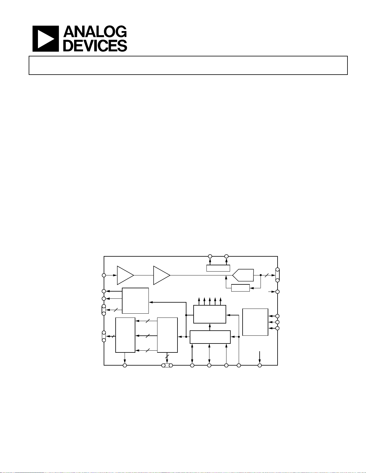
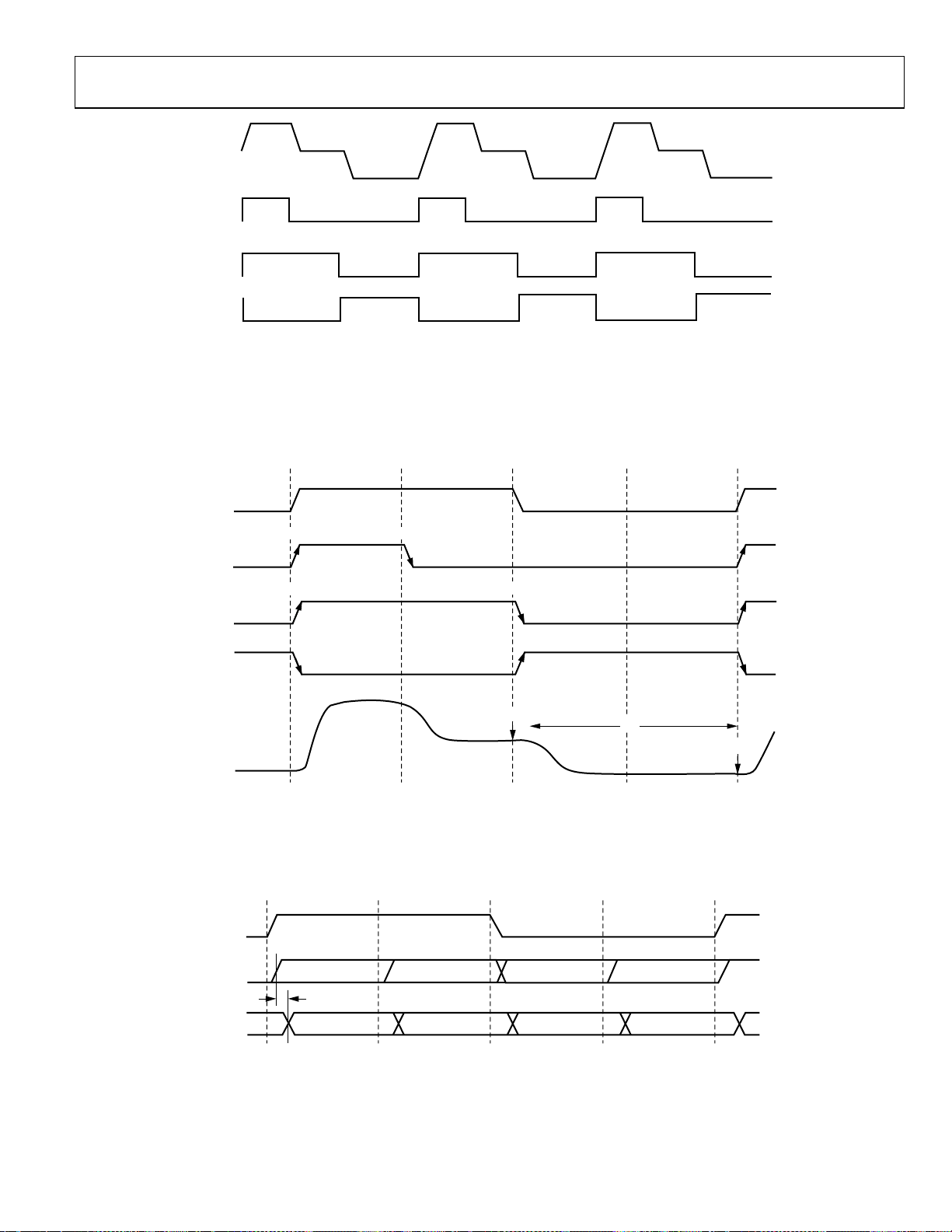
Precision Timing Generator
AD9923A
GENERAL DESCRIPTION
The AD9923A is a complete 36 MHz front-end solution for
digital still cameras and other CCD imaging applications.
Similar to the AD9923 product, the AD9923A includes the
analog front end (AFE), a fully programmable timing generator
(TG), and a 15-channel vertical driver (V-driver). A Precision
Timi ng™core allows adjustment of high speed clocks with
approximately 600 ps resolution at 36 MHz operation.
The on-chip V-driver supports up to 15 channels for use with
5-field, 10-phase CCDs.
The analog front end includes black level clamping, CDS, VGA,
and a 12-bit ADC. The timing generator and V-driver provide
all the necessary CCD clocks: RG, H-clocks, vertical clocks, sensor
gate pulses, substrate clock, and substrate bias control. The
internal registers are programmed using a 3-wire serial
interface.
Packaged in an 8 mm × 8 mm CSP_BGA, the AD9923A is
specified over an operating temperature range of −25°C to +85°C.
CCDIN
RG
H1 TO H4
V1, V2, V3,
4, V5A, V5B,
6, V7A, V7B,
V8, V9, V10,
V11, V12, V13
–3dB, 0dB, +3dB, +6d B
CDS
HL
4
15
V-DRIVER
SUBCK
HORIZONT AL
DRIVERS
XV1 TO
XSG1 TO
XSUBCK,
XSUBCNT
FUNCTIONAL BLOCK DIAGRAM
REFT REFB
+6dB TO +42d B
13
XV13
8
XSG8
2
VGA
VERTICAL
TIMING
CONTROL
3
STROBE
INTERNAL CLOCKS
HD
Figure 1.
VREF
PRECISION
TIMING
GENERATOR
SYNC
GENERATOR
VD SYNC CLI CLOVSUB, MSHUT,
12-BIT
ADC
CLAMP
AD9923A
INTERNAL
REGIS TERS
12
D0 TO D11
DCLK
SL
SDI
SCK
05586-001
Rev. A
Information furnished by Analog Devices is believed to be accurate and reliable. However, no
responsibility is assumed by Analog Devices for its use, nor for any infringements of patents or other
rights of third parties that may result from its use. Specifications subject to change without notice. No
license is granted by implication or otherwise under any patent or patent rights of Analog Devices.
Trademarks and registered trademarks are the property of their respective owners.
One Technology Way, P.O. Box 9106, Norwood, MA 02062-9106, U.S.A.
Tel: 781.329.4700 www.analog.com
Fax: 781.461.3113 ©2006–2010 Analog Devices, Inc. All rights reserved.

AD9923A
TABLE OF CONTENTS
Features .............................................................................................. 1
Theory of Operation ...................................................................... 14
Applications ....................................................................................... 1
General Description ......................................................................... 1
Functional Block Diagram .............................................................. 1
Revision History ............................................................................... 2
Specifications ..................................................................................... 3
Digital Specifications ................................................................... 4
H-Driver Specifications ............................................................... 4
Vertical Driver Specifications ..................................................... 4
Analog Specifications ................................................................... 5
Timing Specifications .................................................................. 6
Absolute Maximum Ratings ............................................................ 8
Thermal Resistance ...................................................................... 8
ESD Caution .................................................................................. 8
Pin Configuration and Function Descriptions ............................. 9
Typical Performance Characteristics ........................................... 11
Precision Timing High Speed Timing Generation ................. 15
Horizontal Clamping and Blanking ......................................... 18
Vertical Timing Generation ...................................................... 24
Vertical Timing Example ........................................................... 38
Vertical Driver Signal Configuration ........................................... 40
Shutter Timing Control ............................................................. 44
Example of Exposure and Readout of Interlaced Frame....... 53
FG_TRIG Operation .................................................................. 54
Analog Front End Description/Operation ............................. 55
Standby Mode Operation .......................................................... 60
Circuit Layout Information ....................................................... 62
Serial Interface Timing .............................................................. 65
Layout of Internal Registers ...................................................... 66
Updating New Register Values ................................................. 67
Complete Register Listing ......................................................... 68
Equivalent Circuits ......................................................................... 12
Terminology .................................................................................... 13
REVISION HISTORY
1/10—Rev. 0 to Rev. A
Changes to Table 6 ............................................................................ 6
Added Table 8; Renumbered Sequentially .................................... 8
Changes to Individual HBLK Patterns Section .......................... 20
Changes to Table 13 ........................................................................ 20
Change to SUBCK: High Precision Operation Section ............. 45
Changes to Manual Control Section ............................................ 49
10/06—Revision 0: Initial Version
Outline Dimensions ....................................................................... 84
Ordering Guide .......................................................................... 84
Rev. A | Page 2 of 84

AD9923A
SPECIFICATIONS
Table 1.
Parameter Conditions/Comments Min Typ Max Unit
TEMPERATURE RANGE
Operating −25 +85 °C
Storage −65 +150 °C
AFETG POWER SUPPLY VOLTAGES
AVDD AFE analog supply 2.7 3.0 3.6 V
TCVDD Timing Core Analog Supply 2.7 3.0 3.6 V
RGVDD RG Driver 2.7 3.0 3.6 V
HVDD HL, H1 to H4 Drivers 2.7 3.0 3.6 V
DRVDD Data Output Drivers 2.7 3.0 3.6 V
DVDD Digital 2.7 3.0 3.6 V
V-DRIVER POWER SUPPLY
VOLTAGES
VDD1, VDD2 V-Driver Logic +2.7 +3.0 +3.6 V
VH1, VH2 V-Driver High Supply +11.5 +15.0 +16.5 V
VL1, VL2 V-Driver Low Supply −8.5 −7.5 −5.5 V
VM1, VM2 V-Driver Mid Supply −1.5 0.0 +1.5 V
VLL SUBCK Low Supply −8.5 −7.5 −5.5 V
VMM SUBCK Mid Supply −4.0 0.0 +1.5 V
AFETG POWER DISSIPATION
Total 36 MHz, 3.0 V supply, 400 pF total H-load, 20 pF RG load 335 mW
Standby 1 Mode 105 mW
Standby 2 Mode 1 mW
Standby 3 Mode 1 mW
Power from HVDD Only
1
Power from RGVDD Only 10 mW
Power from AVDD Only 75 mW
Power from TCVDD Only 40 mW
Power from DVDD Only 75 mW
Power from DRVDD Only 5 mW
V-DRIVER POWER DISSIPATION2
VH1, VH2 5 mW
VL1, VL2 2.5 mW
VM1, VM2 0 mW
VDD1, VDD2 0.5 mW
MAXIMUM CLOCK RATE (CLI) 36 MHz
1
The total power dissipated by the HVDD supply can be approximated using the equation
Total HVDD Power = [C
Reducing the H-load and/or using a lower HVDD supply reduces the power dissipation. C
2
V-driver power dissipation depends on the frequency of operation and the load they are driving. All inputs to the V-driver were tied low for the
measurements in Table 1.
× HVDD × Pixel Frequency] × HVDD
LOAD
130 mW
VH1, VH2 = +15 V; VL1, VL2 = −7.5 V; VM1, VM2 = 0 V; VDD1, VDD2 =
3.3 V; all V-driver inputs tied low
is the total capacitance seen by all H-outputs.
LOAD
Rev. A | Page 3 of 84
AD9923A
DIGITAL SPECIFICATIONS
DRVDD = 2.7 V to 3.6 V, CL = 20 pF, T
Table 2.
Parameter Conditions/Comments Symbol Min Typ Max Unit
LOGIC INPUTS
High Level Input Voltage VIH 2.1 V
Low Level Input Voltage VIL 0.6 V
High Level Input Current IIH 10 μA
Low Level Input Current IIL 10 μA
Input Capacitance CIN 10 pF
LOGIC OUTPUTS Powered by DVDD, DRVDD
High Level Output Voltage At IOH = 2 mA VOH DVDD − 0.5, DRVDD − 0.5 V
Low Level Output Voltage At IOL = 2 mA VOL 0.5 V
H-DRIVER SPECIFICATIONS
HVDD = RGVDD = 2.7 V to 3.6 V, CL = 20 pF, T
Table 3.
Parameter Conditions/Comments Min Typ Max Unit
RG and H-DRIVER OUTPUTS RG, HL, and H1 to H4 powered by RGVDD, HVDD
High Level Output Voltage At maximum current RGVDD − 0.5, HVDD − 0.5 V
Low Level Output Voltage At maximum current 0.5 V
Maximum Output Current Programmable 30 mA
Maximum Load Capacitance For each output 100 pF
MIN
to T
, unless otherwise noted.
MAX
to T
MIN
, unless otherwise noted.
MAX
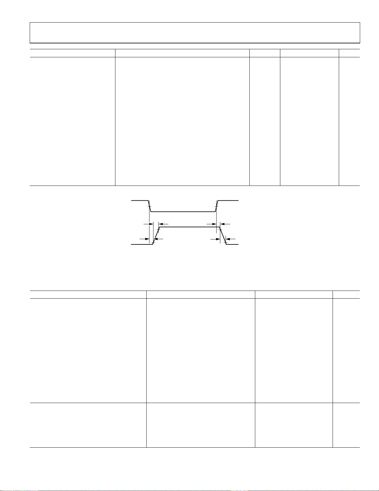
VERTICAL DRIVER SPECIFICATIONS
VDD1 = VDD2 = 3.3 V, VH1 = VH2 = 15 V, VM1 = VM2 = VMM = 0 V, VL1 = VL2 = VLL = −7.5 V, 25°C.
Table 4.
Parameter Conditions/Comments Symbol Min Typ Max Unit
V-DRIVER OUTPUTS Simplified load conditions, 3000 pF to ground
Delay Time
VL to VM and VM to VH Rising edges t
VM to VL and VH to VM Falling edges t
Rise Time
VL to VM t
VM to VH t
Fall Time
VM to VL t
VH to VM t
Output Currents
at −7.25 V +10 mA
at −0.25 V −22 mA
at +0.25 V +22 mA
at +14.75 V −10 mA
RON 35 Ω
SUBCK OUTPUT Simplified load conditions, 1000 pF to ground
Delay Time
VLL to VH t
VH to VLL t
VLL to VMM t
Rev. A | Page 4 of 84
, t
35 ns
PLM
PMH
, t
35 ns
PML
PHM
125 ns
RLM
260 ns
RMH
220 ns
FML
125 ns
FHM
25 ns
PLH
30 ns
PHL
25 ns
PLM
AD9923A
Parameter Conditions/Comments Symbol Min Typ Max Unit
VMM to VH t
VH to VMM t
VMM to VLL t
Rise Time
VLL to VH t
VLL to VMM t
VMM to VH t
Fall Time
VH to VLL t
VH to VMM t
VMM to VLL t
Output Currents
at −7.25 V 20 mA
at −0.25 V 12 mA
at +0.25 V 12 mA
at +14.75 V 20 mA
RON 35 Ω
25 ns
PMH
30 ns
PHM
25 ns
PML
40 ns
RLH
45 ns
RLM
30 ns
RMH
40 ns
FHL
90 ns
FHM
25 ns
FML
V-DRIVER
INPUT
V-DRIVER
OUTPUT
50%
10%
90%
50%
t
,
t
,
RLM
t
PLM
t
RMH
RLH
,
t
,
t
PMH
PLH
90%
10%
t
PML
,
t
,
t
PHM
PHL
t
,
t
,
FHM
t
FHL
5586-002
FML
Figure 2. Definition of V-Driver Timing Specifications
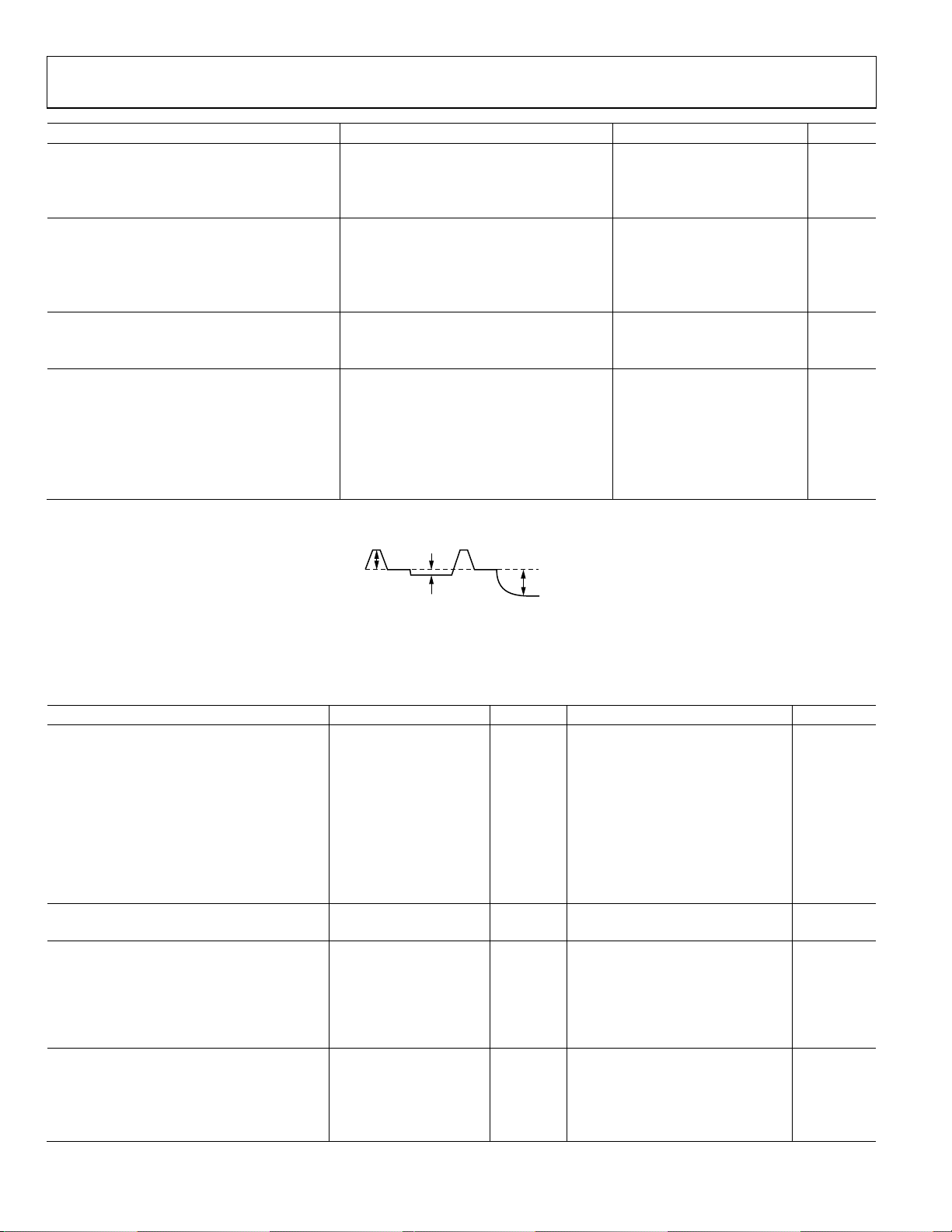
ANALOG SPECIFICATIONS
AVDD = 3.0 V, f
Table 5.
Parameter Conditions/Comments Min Typ Max Unit
CDS Input characteristics definition
Allowable CCD Reset Transient 0.5 1.2 V
CDS Gain Accuracy VGA gain = 6 dB (Code 15, default value)
−3 dB CDS Gain −3 −2.5 −2 dB
0 dB CDS Gain Default 0 +0.5 +1 dB
+3 dB CDS Gain +3 +3.5 +4 dB
+6 dB CDS Gain +5.5 +6 +6.5 dB
Maximum Input Range Before Saturation
0 dB CDS Gain Default setting 1.0 V p-p
−3 dB CDS Gain 1.4 V p-p
+6 dB CDS Gain 0.5 V p-p
Maximum CCD Black Pixel Amplitude Positive offset definition
0 dB CDS Gain (Default) −100 +200 mV
+6 dB CDS Gain −50 +100 mV
VARIABLE GAIN AMPLIFIER (VGA)
Gain Control Resolution 1024 Steps
Gain Monotonicity Guaranteed
Gain Range
Minimum Gain (VGA Code 15) 6 dB
Maximum Gain (VGA Code 1023) 42 dB
= 36 MHz, typical timing specifications, T
CLI
MIN
to T
, unless otherwise noted.
MAX
1
1
Rev. A | Page 5 of 84
AD9923A
Parameter Conditions/Comments Min Typ Max Unit
BLACK LEVEL CLAMP Measured at ADC output
Clamp Level Resolution 1024 Steps
Minimum Clamp Level (Code 0) 0 LSB
Maximum Clamp Level (Code 1023) 255 LSB
ANALOG-TO-DIGITAL CONVERTER (ADC)
Resolution 12 Bits
Differential Nonlinearity (DNL) −1.0 ±0.5 +1.0 LSB
No Missing Codes Guaranteed
Full-Scale Input Voltage 2.0 V
VOLTAGE REFERENCE
Reference Top Voltage (REFT) 2.0 V
Reference Bottom Voltage (REFB) 1.0 V
SYSTEM PERFORMANCE Includes entire signal chain
Gain Accuracy
Low Gain (VGA Code 15) Default CDS gain (0 dB) 6.0 6.5 7.0 dB
Maximum Gain (VGA Code 1023) 42.0 42.5 43.0 dB
Peak Nonlinearity, 500 mV Input Signal 12 dB gain applied 0.1 %
Total Output Noise AC-grounded input, 6 dB gain applied 1.0 LSB rms
Power Supply Rejection (PSR) Measured with step change on supply 50 dB
1
Input signal characteristics are defined as shown in Figure 3.
1V MAX
INPUT SIG NAL RANGE
(0dB CDS GAIN)
500mV TYP
RESET TRANSIENT
TIMING SPECIFICATIONS
CL = 20 pF, AVDD = DVDD = DRVDD = 3.0 V, f
Table 6.
Parameter Conditions/Comments Symbol Min Typ Max Unit
MASTER CLOCK, CLI
CLI Clock Period t
CLI High/Low Pulse Width 11.2 13.9 16.6 ns
Delay from CLI Rising Edge to Internal Pixel
Position 0
AFE CLPOB Pulse Width
1, 2
2 20 Pixels
Allowable Region for HD Falling Edge to CLI
Rising Edge
SHP Inhibit Region Only valid in slave mode t
AFE SAMPLE LOCATION
1
SHP Sample Edge to SHD Sample Edge tS1 11.6 13.9 ns
DATA OUTPUTS
Output Delay from DCLK Rising Edge
1
t
Inhibited Area for DOUTPHASE Edge
Location
Pipeline Delay from SHP/SHD Sampling to
Data Output
SERIAL INTERFACE
Maximum SCK Frequency f
SL to SCK Setup Time tLS 10 ns
SCK to SL Hold Time tLH 10 ns
SDATA Valid to SCK Rising Edge Setup tDS 10 ns
= 36 MHz, unless otherwise noted.
CLI
t
Only valid in slave mode t
SHD SHD + 11 Edge
16 Cycles
200mV MAX
OPTICAL BLACK PIXEL
Figure 3. Signal Characteristics
CONV
CLIDLY
HDCLI
SHPINH
OD
SCLK
05586-003
27.8 ns
6 ns
4 t
− 2 ns
CONV
30 39 Edge
location
8 ns
location
36 MHz
Rev. A | Page 6 of 84
AD9923A
Parameter Conditions/Comments Symbol Min Typ Max Unit
SCK Falling Edge to SDATA Valid Hold tDH 10 ns
SCK Falling Edge to SDATA Valid Read tDV 10 ns
INHIBIT REGION FOR SHP AND SHD WITH
RESPECT TO H-CLOCK EDGE LOCATION
HxMASK = 0, HxRETIME = 0, HxPOLARITY = 0 t
HxMASK = 0, HxRETIME = 0, HxPOLARITY = 1 t
HxMASK = 0, HxRETIME = 1, HxPOLARITY = 0 t
HxMASK = 0, HxRETIME = 1, HxPOLARITY = 1 t
HxMASK = 1, HxRETIME = 0, HxPOLARITY = 0 t
HxMASK = 1, HxRETIME = 0, HxPOLARITY = 1 t
HxMASK = 1, HxRETIME = 1, HxPOLARITY = 0 t
HxMASK = 1, HxRETIME = 1, HxPOLARITY = 1 t
1
Parameter is programmable.
2
Minimum CLPOB pulse width is for functional operation only. Wider typical pulses are recommended to achieve good clamp performance.
HxPOS − 9 HxPOS − 18
SHDINH
Edge
location
HxNEG − 9 HxNEG − 18
SHDINH
Edge
location
HxPOS − 7 HxPOS − 16
SHPINH
Edge
location
HxNEG − 7 HxNEG − 16
SHPINH
Edge
location
HxNEG − 9 HxNEG − 18
SHDINH
Edge
location
HxPOS − 9 HxPOS − 18
SHDINH
Edge
location
HxNEG − 7 HxNEG − 16
SHPINH
Edge
location
HxPOS − 7 HxPOS − 16
SHPINH
Edge
location
Rev. A | Page 7 of 84
AD9923A
ABSOLUTE MAXIMUM RATINGS
Table 7.
Parameter To Rating
AVDD AVSS −0.3 V to +3.9 V
TCVDD TCVSS −0.3 V to +3.9 V
HVDD HVSS −0.3 V to +3.9 V
RGVDD RGVSS −0.3 V to +3.9 V
DVDD DVSS −0.3 V to +3.9 V
DRVDD DRVSS −0.3 V to +3.9 V
VDD1, VDD2 VSS1, VSS2 −0.3 V to +6 V
VH1, VH2 VL1, VL2 −0.3 V to +25 V
VH1, VH2 VSS1, VSS2 −0.3 V to +17 V
VL1, VL2 VSS1, VSS2 −17 V to +0.3 V
VM1, VM2 VSS1, VSS2 −6 V to +6 V
VLL VSS1, VSS2 −17 V to +0.3 V
VMM VSS1, VSS2 −6 V to + VH
VDR_EN VSS1, VSS2 −0.3 V to +6 V
V1 to V15 VSS1, VSS2 VL − 0.3 V to VH + 0.3 V
RG Output RGVSS −0.3 V to RGVDD + 0.3 V
H1 to H4 Output HVSS −0.3 V to HVDD + 0.3 V
Digital Outputs DVSS −0.3 V to DVDD + 0.3 V
Digital Inputs DVSS −0.3 V to DVDD + 0.3 V
SCK, SL, SDATA DVSS −0.3 V to DVDD + 0.3 V
REFT/REFB, CCDIN AVSS −0.3 V to AVDD + 0.3 V
Junction Temperature 150°C
Lead Temperature, 10 sec 350°C
Stresses above those listed under Absolute Maximum Ratings
may cause permanent damage to the device. This is a stress
rating only; functional operation of the device at these or any
other conditions above those indicated in the operational
section of this specification is not implied. Exposure to absolute
maximum rating conditions for extended periods may affect
device reliability.
THERMAL RESISTANCE
Table 8. Thermal Resistance
Package Type θJA Unit
CSP_BGA 40.3 °C/W
ESD CAUTION
Rev. A | Page 8 of 84
AD9923A
PIN CONFIGURATION AND FUNCTION DESCRIPTIONS
AD9923A
A1 CORNER
INDEX AREA
Figure 4. 105-Lead CSPBGA Package Pin Configuration
1234567891011
Table 9. Pin Function Descriptions
Pin No. Mnemonic Type1 Description
A7 AVDD P Analog Supply for AFE.
A1, A4, B2, B3, B4, B5, B6, B7 AVSS P Analog Ground for AFE.
B8 TCVDD P Analog Supply for Timing Core.
B9 TCVSS P Analog Ground for Timing Core.
E1 DVDD1 P Digital Logic Power Supply 1.
F2 DVSS1 P Digital Logic Ground 1.
K8, L7, L8 DVDD2 P Digital Logic Power Supply 2.
K9 DVSS2 P Digital Logic Ground 2.
D9 HVDD P H1 to H4, HL Driver Supply.
D10 HVSS P H1 to H4, HL Driver Ground.
B10 RGVDD P RG Driver Supply.
A10 RGVSS P RG Driver Ground.
L4 DRVDD P Data Output Driver Supply.
L5 DRVSS P Data Output Driver Ground.
J4 VDD1 P V-Driver Logic Supply 1.
K5 VSS1 P V-Driver Logic Ground 1.
L10 VDD2 P V-Driver Logic Supply 2.
K10 VSS2 P V-Driver Logic Ground 2.
F9 VH1 P V-Driver High Supply 1.
D1 VH2 P V-Driver High Supply 2.
E9 VL1 P V-Driver Low Supply 1.
C1 VL2 P V-Driver Low Supply 2.
C9 VM1 P V-Driver Mid Supply 1.
D3 VM2 P V-Driver Mid Supply 2.
F3 VLL P SUBCK Driver Low Supply.
E3 VMM P SUBCK Driver Mid Supply.
A6 CCDIN AI CCD Signal Input.
A5 CCDGND AI CCD Signal Ground.
A3 REFT AO Voltage Reference Top Bypass.
A2 REFB AO Voltage Reference Bottom Bypass.
C3 SL DI 3-Wire Serial Load Pulse.
C2 SCK DI 3-Wire Serial Clock.
B1 SDI DI 3-Wire Serial Data Input.
G7 SYNC DI External System Synchronization Input.
E5
RSTB
TOP VIEW
(Not to Scale)
A
B
C
D
E
F
G
H
J
K
L
05586-004
DI Reset Bar, Active Low Pulse.
Rev. A | Page 9 of 84
AD9923A
Pin No. Mnemonic Type1 Description
A8 CLI DI Reference Clock Input (Master Clock).
A9 CLO DO Clock Output for Crystal.
F11 H1 DO CCD Horizontal Clock 1.
E11 H2 DO CCD Horizontal Clock 2.
D11 H3 DO CCD Horizontal Clock 3.
C11 H4 DO CCD Horizontal Clock 4.
B11 HL DO CCD Last Horizontal Clock.
C10 RG DO CCD Reset Gate Clock.
K6 VSUB DO CCD Substrate Bias.
F5 MSHUT DO Mechanical Shutter Pulse.
G5 STROBE DO Strobe Pulse.
G6 SUBCK DO CCD Substrate Clock (E Shutter).
F1 DCLK DO Data Clock Output.
G1 D0 DO Data Output (LSB).
H3 D1 DO Data Output.
H2 D2 DO Data Output.
H1 D3 DO Data Output.
J3 D4 DO Data Output.
J2 D5 DO Data Output.
J1 D6 DO Data Output.
K3 D7 DO Data Output.
K2 D8 DO Data Output.
K1 D9 DO Data Output.
L3 D10 DO Data Output.
L2 D11 DO Data Output (MSB).
D2 VD DIO Vertical Sync Pulse. Input in slave mode, output in master mode.
E2 HD DIO Horizontal Sync Pulse. Input in slave mode, output in master mode.
C8 V1 VO3 CCD Vertical Transfer Clock.
G10 V2 VO2 CCD Vertical Transfer Clock.
E7 V3 VO3 CCD Vertical Transfer Clock.
G9 V4 VO2 CCD Vertical Transfer Clock.
C4 V5A VO3 CCD Vertical Transfer Clock.
C5 V5B VO3 CCD Vertical Transfer Clock.
F10 V6 VO2 CCD Vertical Transfer Clock.
C6 V7A VO3 CCD Vertical Transfer Clock.
C7 V7B VO3 CCD Vertical Transfer Clock.
G11 V8 VO2 CCD Vertical Transfer Clock.
H11 V9 VO2 CCD Vertical Transfer Clock.
H10 V10 VO2 CCD Vertical Transfer Clock.
F6 V11 VO3 CCD Vertical Transfer Clock.
F7 V12 VO3 CCD Vertical Transfer Clock.
E10 V13 VO2 CCD Vertical Transfer Clock.
K11 VDR_EN DI V-Driver Output Enable pin.
J5 TEST0 DI Test Input. Must be tied to VSS1 or VSS2.
J7 TEST1 DI Test Input. Must be tied to VSS1 or VSS2.
J8 TEST3 DI Test Input. Must be tied to VDD1 or VDD2.
A11, E6, H9, J6, J9, J10, J11, K4, K7, L1, L6,
L9, L11, G2, G3
1
AI = analog input, AO = analog output, DI = digital input, DO = digital output, DIO = digital input/output, P = power, VO2 = Vertical Driver Output 2 level, VO3 =
Vertical Driver Output 3 level.
NC No Connect.
Rev. A | Page 10 of 84
AD9923A
TYPICAL PERFORMANCE CHARACTERISTICS
450
400
350
300
250
200
POWER (V)
150
100
50
0
18
FREQUENCY (MHz)
3.3V
3.0V
2.7V
27
36
05586-089
Figure 5. Power vs. Sample Rate
5
4
3
2
1
INL (LSB)
0
–1
–2
–3
0 500 1000 1500 2000 2500 3000 3500
CODE
Figure 7. Typical INL Performance
4000
05586-087
0.6
0.4
0.2
0
DNL (LSB)
–0.2
–0.4
–0.6
0 500 1000 1500 2000 2500 3000 3500
CODE
Figure 6. Typical DNL Performance
4000
55
50
45
40
35
30
25
20
NOISE LSB ( rms)
15
10
5
0
0
05586-086
GAIN CODE
+6dB
+3dB
–3dB
0dB
1000900800700600500400300200100
05586-088
Figure 8. Output Noise vs. VGA Gain
Rev. A | Page 11 of 84
AD9923A
V
EQUIVALENT CIRCUITS
HVDD OR RGVDD
AVDD
R
AVSS
AVSS
05586-005
Figure 9. CCDIN, CCDGND
DVDD
DATA
THREE-STAT E D[0:11]
DVSS DRVSS
DRVDD
RG, HL,
H1 TO H4
THREE-STATE OUTPUT
HVSS OR RGVSS
05586-008
Figure 12. HL, H1 to H4, and RG Drivers
DVDD
VDVSS
3.5kΩ
R
05586-009
VDR_EN
Figure 13. VDR_EN Input
5586-006
Figure 10. Digital Data Outputs
DVDD
330Ω
DVSS
05586-007
Figure 11. Digital Inputs
Rev. A | Page 12 of 84

AD9923A
TERMINOLOGY
Differential Nonlinearity (DNL)
An ideal ADC exhibits code transitions that are exactly 1 LSB
apart. DNL is the deviation from this ideal value. Therefore,
every code must have a finite width. No missing codes guaranteed
to 12-bit resolution indicates that all 4096 codes, respectively,
must be present over all operating conditions.
Integral Nonlinearity (INL)
The deviation of each code measured from a true straight line
between the zero and full-scale values. The point used as zero
scale occurs 0.5 LSB before the first code transition. Positive full
scale is defined as a level 1.5 LSB beyond the last code transition.
The deviation is measured from the middle of each output code
to the true straight line.
Peak Nonlinearity
Peak nonlinearity, a full signal chain specification, refers to the
peak deviation of the AD9923A output from a true straight line.
The point used as zero scale occurs 0.5 LSB before the first code
transition. Positive full scale is defined as a level 1.5 LSB beyond
the last code transition. The deviation is measured from the
middle of each output code to the true straight line. The error is
expressed as a percentage of the 2 V ADC full-scale signal. The
input signal is always appropriately gained up to fill the full-scale
range of the ADC.
Tot a l O ut p ut Noi se
The rms output noise is measured using histogram techniques.
The standard deviation of the ADC output codes is calculated
in LSB, and represents the rms noise level of the total signal
chain at the specified gain setting. The output noise can be
converted to an equivalent voltage, using the relationship
1 LSB = (ADC full scale/2
where n is the bit resolution of the ADC and 1 LSB is 0.488 mV.
Power Supply Rejection (PSR)
The PSR is measured with a step change applied to the supply
pins. The PSR specification is calculated from the change in the
data outputs for a given step change in the supply voltage.
n
codes)
Rev. A | Page 13 of 84
AD9923A
V
THEORY OF OPERATION
Figure 14 shows the typical system block diagram for the
AD9923A in master mode. The CCD output is processed by
the AD9923A AFE circuitry, which consists of a CDS, VGA,
black level clamp, and ADC. The digitized pixel information is
sent to the digital image processor chip that performs the postprocessing and compression. To operate the CCD, CCD timing
parameters are programmed into the AD9923A from the system
microprocessor through the 3-wire serial interface. The AD9923A
generates the CCD horizontal, vertical, and the internal AFE
clocks from the system master clock CLI. The CLI is provided
by the image processor or external crystal. External synchronization is provided by a sync pulse from the microprocessor, which
resets internal counters and resyncs the VD and HD outputs.
Alternatively, the AD9923A can be operated in slave mode, in
which the VD and HD are provided externally from the image
processor. In this mode, the AD9923A timing is synchronized
with VD and HD.
The H-drivers for HL, H1 to H4, and RG are included in the
AD9923A, allowing these clocks to be directly connected to the
CCD. An H-driver voltage, HVDD, of up to 3.3 V is supported.
An external V-driver is required for the vertical transfer clocks,
the sensor gate pulses, and the substrate clock.
Figure 15 and Figure 16 show the maximum horizontal and
vertical counter dimensions for the AD9923A. Internal horizontal and vertical clocking is controlled by these counters to
specify line and pixel locations. The maximum HD length is
8192 pixels per line, and the maximum VD length is 4096 lines
per field.
1 TO V13, SUBCK
HL, H1 TO H4, RG, VSUB
SERIAL
INTERFACE
D[0:11]
DCLK
HD, VD
CLI
DIGITAL
IMAGE
PROCESSING
ASIC
MICRO-
PROCESSOR
CCD
CCDIN
MSHUT
STROBE
AD9923A
V-DRIVER
SYNC
AFETG +
Figure 14. Typical System Block Diagram, Master Mode
MAXIMUM
COUNTER
DIMENSIONS
13-BIT HORIZONTAL = 8192 PIXELS MAX
05586-013
The AD9923A also includes programmable MSHUT and
STROBE outputs that can be used to trigger mechanical shutter
and strobe (flash) circuitry.
MAX VD LENGTH IS 4096 LI NES
VD
HD
CLI
MAX HD LENGT H IS 8192 PIX ELS
Figure 16. Maximum VD/HD Dimensions
12-BIT VERT ICAL = 4096 LINES MAX
05586-014
Figure 15. Vertical and Horizontal Counters
05586-015
Rev. A | Page 14 of 84

AD9923A
PRECISION TIMING
HIGH SPEED TIMING GENERATION
The AD9923A generates high speed timing signals using the
flexible Precision Timing core. This core is the foundation for
generating the timing used for both the CCD and the AFE. It
consists of the reset gate (RG), horizontal drivers (H1 to H4 and
HL), and sample clocks (SHP and SHD). A unique architecture
makes it routine for the system designer to optimize image
quality by providing precise control over the horizontal CCD
readout and the AFE-correlated double sampling.
The high speed timing of the AD9923A operates the same in
master and slave modes. For more information on synchroniza-
tion and pipeline delays, see the Power-Up and Synchronization
in Slave Mode section.
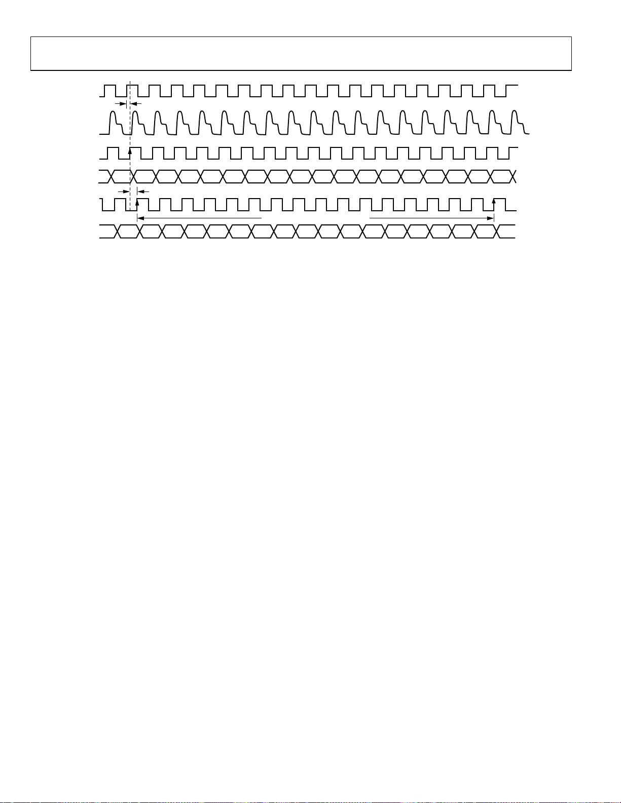
Timing Resolution
The Precision Timing core uses a 1× master clock input (CLI) as
a reference. The frequency of this clock should match the CCD
pixel clock frequency. Figure 17 illustrates how the internal
timing core divides the master clock period into 48 steps, or
edge positions. Using a 36 MHz CLI frequency, the edge
resolution of the Precision Timing core is approximately 0.6 ns.
If a 1× system clock is not available, a 2× reference clock can be
used by programming the CLIDIVIDE register (Address 0x30).
The AD9923A then internally divides the CLI frequency by 2.
The AD9923A includes a master clock output (CLO) which is
the inverse of CLI. This output is intended to be used as a
crystal driver. A crystal can be placed between the CLI and
CLO pins to generate the master clock for the AD9923A. For
more information on using a crystal, see Figure 80.
High Speed Clock Programmability
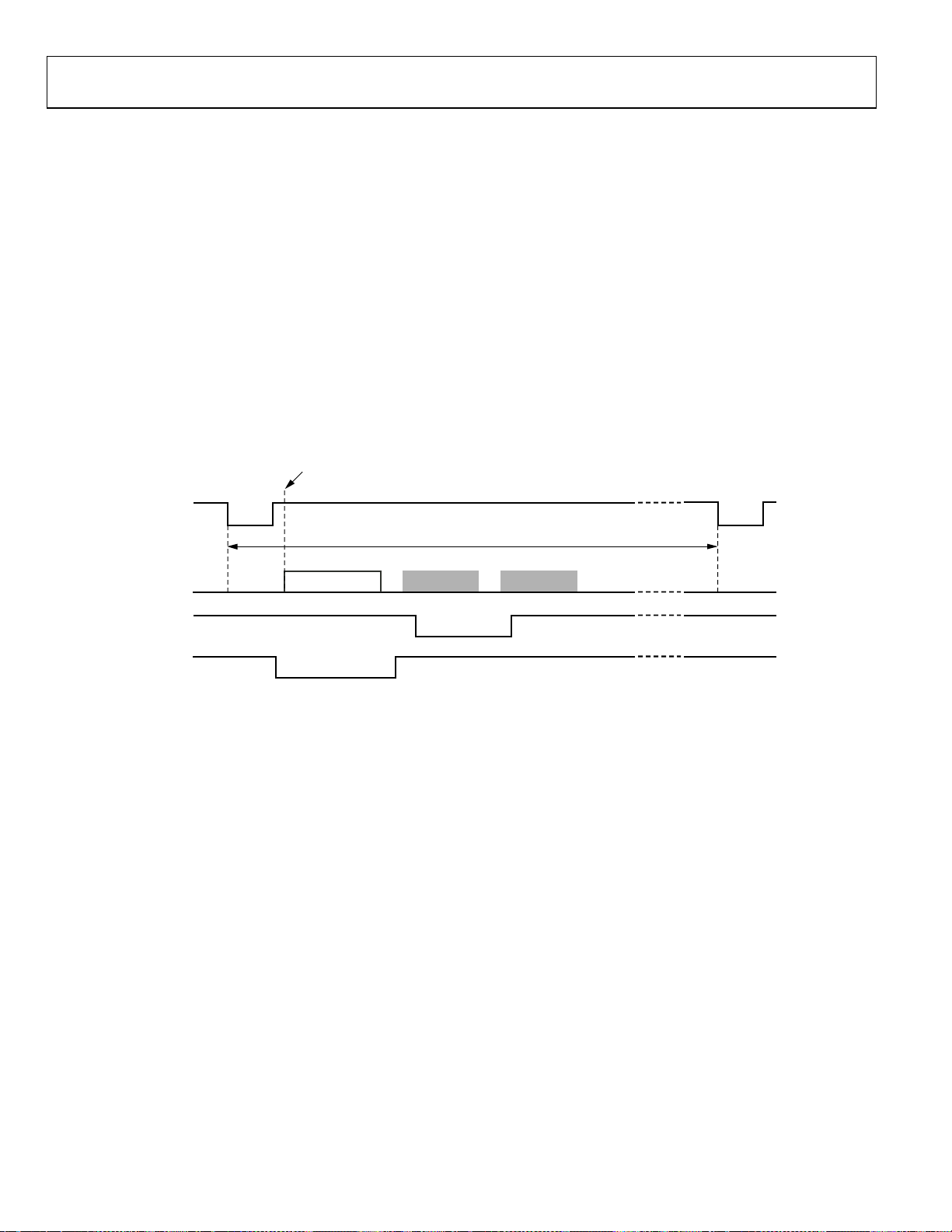
Figure 18 shows how the RG, HL, H1 to H4, SHP, and SHD
high speed clocks are generated. The RG pulse has programmable
rising and falling edges and can be inverted using the polarity
control. The HL, H1, and H3 horizontal clocks have program-
mable rising and falling edges and polarity control. The H2 and
H4 clocks are inverses of the H1 and H3 clocks, respectively.
Tabl e 10 summarizes the high speed timing registers and their
parameters. Figure 19 shows the typical 2-phase, H-clock
operation, in which H3 and H4 are programmed for the same
edge location as H1 and H2.
The edge location registers are six bits wide, but there are only
48 valid edge locations available. Therefore, the register values
are mapped into four quadrants, each of which contains 12 edge
locations. Tabl e 11 shows the correct register values for the
corresponding edge locations. Figure 20 shows the default
timing locations for high speed clock signals.
H-Driver and RG Outputs
In addition to the programmable timing positions, the
AD9923A features on-chip output drivers for the RG and H1 to
H4 outputs. These drivers are powerful enough to directly drive
the CCD inputs. The H-driver and RG current can be adjusted for
optimum rise/fall times in a particular load by using the H1 to
H4, HL, and RGDRV registers (Address 0x36). The 3-bit drive
setting for each output can be adjusted in 4.1 mA increments,
with the minimum setting of 0 equal to 0 mA or three-state, and
the maximum setting of 7 equal to 30.1 mA.
As shown in Figure 18, Figure 19, and Figure 20, the H2 and H4
outputs are inverses of H1 and H3 outputs, respectively. The
H1/H2 crossover voltage is approximately 50% of the output
swing. The crossover voltage is not programmable.
Digital Data Outputs
The AD9923A data output and DCLK phase are programmable
using the DOUTPHASE register (Address 0x38, Bits[5:0]). Any
edge from 0 to 47 can be programmed, as shown in Figure 21.
Normally, the DOUT and DCLK signals track in phase, based
on the DOUTPHASE register contents. The DCLK output
phase can also be held fixed with respect to the data outputs by
setting the DCLKMODE register to high (Address 0x38, Bit[8]).
In this mode, the DCLK output remains at a fixed phase equal
to a delayed version of CLI, and the data output phase remains
programmable. For more detail, see the Analog Front End
Description/Operation section.
There is a fixed output delay from the DCLK rising edge to the
DOUT transition, called t
four values between 0 ns and 12 ns, using the DOUTDELAY
register (Address 0x38, Bits[10:9]). The default value is 8 ns.
The pipeline delay through the AD9923A is shown in Figure 22.
After the CCD input is sampled by SHD, there is a 16-cycle
delay before the data is available.
. This delay can be programmed to
OD
Table 10. Timing Core Register Parameters for HL, H1 to H4, RG, SHP/SHD
Length
Parameter
Polarity 1 High/low Polarity control for HL, H1, H3, and RG (0 = no inversion, 1 = inversion)
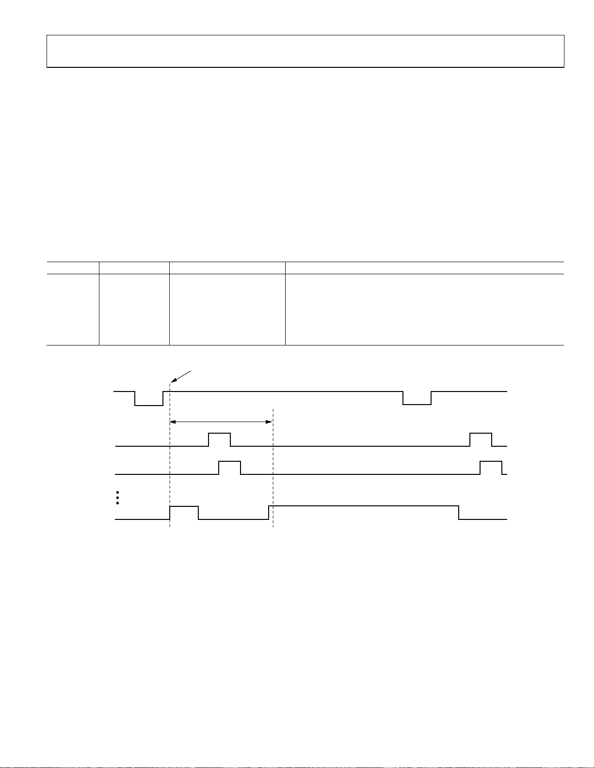
Positive Edge 6 0 to 47 edge location Positive edge location for HL, H1, H3, and RG (H2/H4 are inverses of H1/H3, respectively)
Negative Edge 6 0 to 47 edge location Negative edge location for HL, H1, H3, and RG (H2/H4 are inverses of H1/H3, respectively)
Sampling
Location
Drive Strength 3 0 to 7 current steps Drive current for HL, H1 to H4, and RG outputs (4.1 mA per step)
(Bits) Range Description
6 0 to 47 edge location Sampling location for internal SHP and SHD signals
Rev. A | Page 15 of 84
AD9923A
Table 11. Precision Timing Edge Locations
Quadrant Edge Location (Decimal) Register Value (Decimal) Register Value (Binary)
I 0 to 11 0 to 11 000000 to 001011
II 12 to 23 16 to 27 010000 to 011011
III 24 to 35 32 to 43 100000 to 101011
IV 36 to 47 48 to 59 110000 to 111011
POSITION
CLI
1 PIXEL
PERIOD
P[0] P[48] = P[0]P[12] P[24] P[36]
t
CLIDLY
NOTES
1. THE PIXEL CLOCK PE RIOD IS DI VIDED INT O 48 POSITIONS, PROVIDING FINE EDG E RESOLUT ION FO R HIGH SPEED CLOCK.
2. THERE IS A FIXED DELAY FROM THE CLI INPUT TO THE INTERNAL PIXEL PERIOD POSITION (t
CLIDLY
= 6ns TYP ).
Figure 17. High Speed Clock Resolution from CLI Master Clock Input
3
CCD
SIGNAL
12
RG
56
HL
78
H1
4
05586-016
H2
910
H3
H4
PROGRAMMABLE CLOCK POSI TIONS:
1
RG RISING E DGE.
2
RG FALLING EDGE.
3
SHP SAMPLE LOCATION.
4
SHD SAMPLE LOCATION.
5
HL RISING E DGE POSITION.
6
HL FALLING EDGE POSITION.
7
H1 RISING EDGE POSITION.
8
H1 FALLING EDGE POSITION (H2 IS INVERSE OF H1).
9
H3 RISING EDGE POSITION.
10
H3 FALLING EDGE POSITION (H4 IS INVERSE OF H3).
05586-017
Figure 18. High Speed Clock Programmable Locations
Rev. A | Page 16 of 84
AD9923A
2
3
CCD
SIGNAL
RG
HL/H1/H3
H2/H4
NOTES
1. USING T HE SAME TOG GLE PO SITIO NS FOR H1 AND H3 GENERATES STANDARD 2-PHASE H-CLOCKI NG.
Figure 19. 2-Phase H-Clock Operation
05586-018
POSITION
PIXEL
PERIOD
RG
HL/H1/H3
H2/H4
CCD
SIGNAL
NOTES
1. ALL SIGNAL EDGES ARE FULLY PROGRAMMABLE TO ANY OF THE 48 POSITIONS WITHIN ONE PIXEL PERIOD.
2. DEFAULT POSITIONS FOR EACH SIGNAL ARE SHOWN.
P[0]
RGr[0] RGf[12]
Hr[0] Hf[24]
P[24]P[12] P [36]
SHP[24]
t
S1
P[48] = P[0]
SHD[48]
5586-019
Figure 20. High Speed Timing Default Locations
P[0]
P[12]
P[24]
P[36]
P[48] = P[0]
PIXEL
PERIOD
DCLK
t
OD
DOUT
NOTES
1. DATA OUTP UT (DOUT) AND DCL K PHASE ARE ADJUSTABLE WITH RES PECT TO THE PIXEL PERIOD.
. WITHIN 1 CLOCK PERI OD, THE DAT A TRANSITI ON CAN BE PROG RAMMED TO 48 DI FFERENT LOCATIONS.
. OUTPUT DELAY (
t
) FROM DCLK RI SING EDGE TO DOUT RI SING EDG E IS PROGRAMMABLE.
OD
05586-020
Figure 21. Digital Output Phase Adjustment
Rev. A | Page 17 of 84
AD9923A
CLI
t
CCDIN
SHD
(INTERNAL)
ADC DOUT
(INTERNAL)
DCLK
D[0:11]
CLIDLY
NN+1
SAMPLE PIXEL N
N–17
N–17
NOTES
1. TIMING VALUES SHO WN ARE SHDLO C = 0, WITH DCLKMODE = 0.
2. HIGHER VAL UES OF SHD AND/OR DOUTPHASE S HIFT DOUT TRANSITION TO T HE RIGHT WITH RESPE CT TO CLI LOCATI ON.
3. INHIBIT TIME F OR DOUT PHASE IS DEFI NED BY
THE 12 EDGE LOCATIONS F OLLO WING SHDL OC NOT BE USED FOR THE DOUTPHASE LOCATION.
4. RECOMMENDED VALUE FOR DOUT PHASE IS TO USE THE SHPLOC EDGE OR THE 11 EDGES FOLLOWING SHPLOC.
5. RECOMMENDED V ALUE FOR
6. THE DOUT LATCH CAN BE BYPASSED USING REG ISTER 0x01, BIT [1] = 1 SO THAT THE ADC DATA OUTPUTS APPEAR DIRECTLY AT
THE DATA OUTPUT PINS. THIS CONFI GURATION IS RECOMMENDED IF THE ADJUST ABLE DOUT PHASE IS NOT REQUIRED.
N–16
N–16
t
DOUTINH
N+2
N–15
N+3
N–14
N–13
t
(DOUT DLY) IS 4ns.
OD
PIPELI NE LATENCY = 16 CY CLES
t
DOUTINH
N+8N+7N+6N+5N+4
N–8N–9N–10N–11N–12N–13N–14N–15
, WHICH IS EQUAL TO SHDLOC PLUS 11 EDGES. IT IS RECO MMENDED THAT
N+11N+10N+9
N–7 N–6
N–5
N–4
N–4
N–5N–6N–7N–8N–9N–10N–11N–12
N–3
N–3
N+15N+14N+13N+12
N–2NN–1
N–2NN–1
Figure 22. Digital Data Output Pipeline Delay
N+16
N+17
05586-021
HORIZONTAL CLAMPING AND BLANKING
The AD9923A horizontal clamping and blanking pulses are
fully programmable to suit a variety of applications. Individual
controls are provided for CLPOB, PBLK, and HBLK during
different regions of each field. This allows dark pixel clamping
and blanking patterns to be changed at each stage of the readout
to accommodate different image transfer timing and high speed
line shifts.
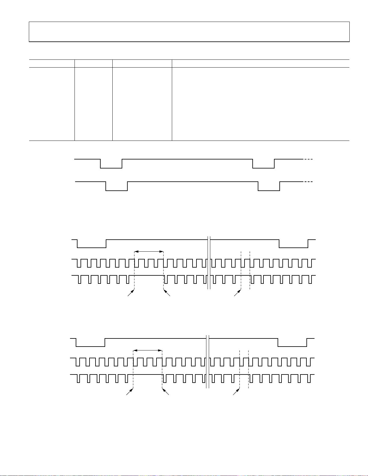
Individual CLPOB and PBLK Patterns
The AFE horizontal timing consists of CLPOB and PBLK, as
shown in Figure 23. These two signals are independently
programmed using the registers in Tab le 1 2 . SPOL is the start
polarity for the signal, and TOG1 and TOG2 are the first and
second toggle positions of the pulse. Both signals are active low
and should be programmed accordingly.
A separate pattern for CLPOB and PBLK can be programmed
for each V-sequence. As described in the Ver tic a l Ti m ing
Generation section, several V-sequences can be created, each
containing a unique pulse pattern for CLPOB and PBLK.
Figure 46 shows how the sequence change positions divide the
readout field into regions. A different V-sequence can be
assigned to each region, allowing the CLPOB and PBLK signals
to change with each change in the vertical timing. Unused CLPOB
and PBLK toggle positions should be set to 8191.
CLPOB and PBLK Masking Area
The AD9923A allows the CLPOB and/or PBLK signals to be
disabled during certain lines in the field without changing the
existing CLPOB and/or PBLK pattern settings.
To use CLPOB masking, the CLPMASKSTART and CLPMASKEND
registers are programmed to specify the starting and ending lines
in the field where the CLPOB patterns are ignored. There are three
sets of CLPMASKSTART and CLPMASKEND registers,
allowing up to three CLPOB masking areas to be created.
CLPOB masking registers are not specific to a given V-sequence;
they are active for any existing field of timing. To disable the
CLPOB masking feature, set these registers to the maximum
value, 0xFFF (default value).
To use PBLK masking, the PBLKMASKSTART and
PBLKMASKEND registers are programmed to specify the
starting and ending lines in the field where the PBLK patterns
are ignored. There are three sets of PBLKMASKSTART and
PBLKMASKEND registers, allowing the creation of up to three
PBLK masking areas.
PBLK masking registers are not specific to a given V-sequence;
they are active for any existing field of timing. To disable the
PBLK masking feature, set these registers to the maximum
value, 0xFFF (default value).
Rev. A | Page 18 of 84
AD9923A
C
K
Table 12. CLPOB and PBLK Pattern Registers
Register Length (Bits) Range Description
CLPOBPOL 1 High/low Starting polarity of CLPOB for each V-sequence
PBLKPOL 1 High/low Starting polarity of PBLK for each V-sequence
CLPOBTOG1 13 0 to 8191 pixel location First CLPOB toggle position within the line for each V-sequence
CLPOBTOG2 13 0 to 8191 pixel location Second CLPOB toggle position within the line for each V-sequence
PBLKTOG1 13 0 to 8191 pixel location First PBLK toggle position within the line for each V-sequence
PBLKBTOG2 13 0 to 8191 pixel location Second PBLK toggle position within the line for each V-sequence
CLPMASKSTART 12 0 to 4095 line location CLPOB masking area—starting line within the field (maximum of three areas)
CLPMASKEND 12 0 to 4095 line location CLPOB masking area—ending line within the field (maximum of three areas)
PBLKMASKSTART 12 0 to 4095 line location PBLK masking area—starting line within the field (maximum of three areas)
PBLKMASKEND 12 0 to 4095 line location PBLK masking area—ending line within the field (maximum of three areas)
HD
32
CLPOB
1
PBLK
PROGRAMMABLE SETTINGS:
1
START POLARITY (CLAMP AND BLANK REGIO NS ARE ACTIVE L OW).
2
FIRST TOGGLE POSITION.
3
SECOND TOGGLE POSITION.
ACTIVE
Figure 23. Clamp and Preblank Pulse Placement
ACTIVE
05586-022
NO CLPOB SI GNAL
FOR LINE 600
NO PBLK SIG NAL
FOR LINE 703
05586-023
5586-010
LPOB
PBL
VD
0 1 2 597 598
HD
CLPMASKSTART 1 = 6 CLPMASKEND1 = 8
NO CLPOB SI GNAL
FOR LINES 6 TO 8
Figure 24. CLPOB Masking Example
VD
0 1 2 700 701
HD
PBLKMASKSTART 1 = 6 PBLKMASKEND1 = 8
NO PBLK SIG NAL
FOR LINES 6 TO 8
Figure 25. PBLK Masking Example
CLPMASKSTART 2 = CLPMASKEND2 = 600
PBLKMASKSTART2 = PBLKMASKEND2 = 703
Rev. A | Page 19 of 84
AD9923A
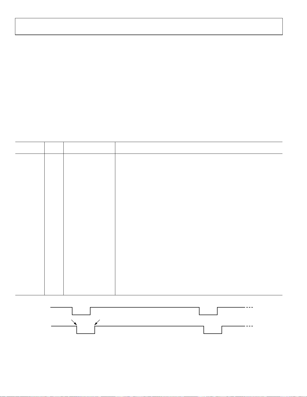
Individual HBLK Patterns
The HBLK programmable timing shown in Figure 26 is similar
to CLPOB and PBLK; however, there is no start polarity control.
Only the toggle positions are used to designate the start and end
positions of the blanking period. Additionally, there is a polarity
control register, HBLKMASK, that designates the polarity of the
horizontal clock signals during the blanking period. Setting
HBLKMASK high sets H1 = H3 = high and H2 = H4 = low
during blanking, as shown in Figure 27. As with CLPOB and
PBLK registers, HBLK registers are available in each V-sequence,
allowing different blanking signals to be used with different
vertical timing sequences.
Note that 8189 is the recommended setting for any unused
HBLK toggle locations on the AD9923A, regardless of the
Table 13. HBLK Pattern Registers
Length
Register
(Bits) Range Description
HBLKMASK 1 High/low Masking polarity for H1, H3, HL (0 = mask low, 1 = mask high)
HBLKALT 3 0 to 7 alternation modes Enables different odd/even alternation of HBLK toggle positions
0: disable alternation (HBLKTOGE1 to HBLKTOGE6 registers are used for each line)
1: TOGE1 and TOGE2 odd lines, TOGE3 to TOGE6 even lines
2: TOGE1 and TOGE2 even lines, TOGE3 to TOGE6 odd lines
3: TOGE1 to TOGE6 even lines, TOGO1 to TOGE6 odd lines (FREEZE/RESUME not
available)
4 to 7: HBLKSTART, HBLKEND, HBLKLEN, and HBLKREP registers are used for each line
HBLKTOGE1 13 0 to 8189 pixel location HBLK first toggle position (for even lines only when HBLKALT = 3)
HBLKTOGE2 13 0 to 8189 pixel location HBLK second toggle position (for even lines only when HBLKALT = 3)
HBLKTOGE3 13 0 to 8189 pixel location HBLK third toggle position (for even lines only when HBLKALT = 3)
HBLKTOGE4 13 0 to 8189 pixel location HBLK fourth toggle position (for even lines only when HBLKALT = 3)
HBLKTOGE5 13 0 to 8189 pixel location Fifth toggle position, even lines (HBLKSTART when HBLKALT = 4 to 7)
HBLKTOGE6 13 0 to 8189 pixel location Sixth toggle position, even lines (HBLKEND when HBLKALT = 4 to 7)
HBLKLEN 13 0 to 8189 pixels HBLK pattern length, only used when HBLKALT = 4 to 7
HBLKREP 8 0 to 255 repetitions Number of HBLK pattern repetitions, only used when HBLKALT = 4 to 7
HBLKTOGO1 13 0 to 8189 pixel location First toggle position for odd lines when HBLKALT = 3 (usually VREPA_3)
HBLKTOGO2 13 0 to 8189 pixel location Second toggle position for odd lines when HBLKALT = 3 (usually VREPA_4)
HBLKTOGO3 13 0 to 8189 pixel location Third toggle position for odd lines when HBLKALT = 3 (usually FREEZE1)
HBLKTOGO4 13 0 to 8189 pixel location Fourth toggle position for odd lines when HBLKALT = 3 (usually RESUME1)
HBLKTOGO5 13 0 to 8189 pixel location Fifth toggle position for odd lines when HBLKALT = 3 (usually FREEZE2)
HBLKTOGO6 13
0 to 8189 pixel location
Sixth toggle position for odd lines when HBLKALT = 3 (usually RESUME2)
setting for HBLKALT. 8190 and 8191 are not valid settings for
HBLK toggle positions that are unused and causes undesired
HBLK toggle activity.
Generating Special HBLK Patterns
There are six toggle positions available for HBLK. Normally,
only two of the toggle positions are used to generate the
standard HBLK interval. However, additional toggle positions
can be used to generate special HBLK patterns, as shown in
Figure 28. The pattern in this example uses all six toggle
positions to generate two extra groups of pulses during the
HBLK interval. By changing the toggle positions, different
patterns can be created.
HBLK
HD
HBLKTOGE1 HBLKTOGE2
BLANK BLANK
BASIC HBLK PULSE IS GENERAT ED USING HBLKT OGE1 AND HBLKTOGE2 REG ISTERS (HBLKALT = 0).
Figure 26. Typical Horizontal Blanking (HBLK) Pulse Placement
Rev. A | Page 20 of 84
05586-024
AD9923A
HD
HBLK
HL/H1/H3
THE POLARI TY OF HL/H1/H3 DURING BLANKING ARE I NDEPENDENTLY P ROGRAMMABLE
(H2/H4 IS OPPOSITE POLARITY OF H1/H3).
H1/H3
H2/H4
...
...
05586-025
Figure 27. HBLK Masking Polarity Control
HBLKTOGE2
HBLKTOGE1
HBLK
HBLKTOGE4
HBLKTOGE3
HBLKTOGE6
HBLKTOGE5
HL/H1/ H3
H2/H4
SPECIAL H-BL ANK PATTERN IS CREATED USING M ULTIPL E HBLK TOG GLE PO SITIO NS (HBLKALT = 0).
Figure 28. Using Multiple Toggle Positions for HBLK (HBLKALT = 0)
Generating HBLK Line Alternation
The AD9923A can alternate different HBLK toggle positions on
odd and even lines. This feature can be used in conjunction with
V-pattern odd/even alternation, or on its own. When 1 is written
to the HBLKALT register, HBLKTOGE1 and HBLKTOGE2 are
used on odd lines, and HBLKTOGE3 to HBLKTOGE6 are used
on even lines. Writing 2 to the HBLKALT register gives the opposite result: HBLKTOGE1 and HBLKTOGE2 are used on even
lines, and HBLKTOGE3 to HBLKTOGE6 are used on odd lines.
When 3 is written to the HBLKALT register, all six even toggle
positions, HBLKTOGE1 to HBLKTOGE6, are used on even
5586-026
lines. There are also six additional toggle positions, HBLKTOGO1
to HBLKTOGE6, for odd lines. These registers are normally
used for VPAT Group A, VPAT Group B, and freeze/resume
functions, but when HBLKALT = 3, these registers become the
odd line toggle positions for HBLK.
Another HBLK feature is enabled by writing 4, 5, 6, or 7 to
HBLKALT. In these modes, the HBLK pattern is generated using
a different set of registers—HBLKSTART, HBLKEND, HBLKLEN,
and HBLKREP—along with four toggle positions. This allows
for multiple repeats of the HBLK signal, as shown in Figure 32.
Rev. A | Page 21 of 84
AD9923A
HD
HBLK
HL/H1/H3
H2/H4
ODD LINE EVEN LINE
HBLKTOGE1
HBLKTOGE2
HBLKTOGE3 HBLKT OGE5
HBLKTOGE4 HBLKT OGE6
ALTERNATING H-BLANK PATTERN USING HBLKAL T = 1 MODE.
05586-027
Figure 29. HBLK Odd/Even Alternation Using HBLKALT = 1
HD
HBLK
HL/H1/H3
H2/H4
ODD LINE EVEN LINE
HBLKTOGE4 HBLKTOG E6 HBLKTO GE2
HBLKTOGE3 HBLKTO GE5 HBLKTOGE1
ALTERNATING H-BLANK PATTERN USING HBLKAL T = 2 MODE.
Figure 30. HBLK Odd/Even Alternation Using HBLKALT = 2
05586-028
HD
HBLK
ODD LINE EVEN LINE
HBLKTOGO2 HBLKTOGO4 HBLKTOGE2 HBLKTOGE 4
HBLKTOGO1 HBLKTO GO3 HBLKTOGE1 HBLKTOGE3
HBLK
HL/H1/H3
H2/H4
HL/H1/H3
H2/H4
HBLKSTART
ALTERNATING H-BLANK PATTERN USING HBLKAL T = 3 MODE.
(FREEZE/ RESUME FUNCTI ON NOT AVAI LABLE IN T HIS MODE.)
Figure 31. HBLK Odd/Even Alternation Using HBLKALT = 3
HBLKTOGE1 HBLKTOGE3
HBLKLEN
HBLKREP = 3
HBLKREP NUMBER 1 HBLKRE P NUMBER 2 HBLKREP NUMBER 3
H-BLANK REPEATING PATTERN IS CREATED USING HBLKLEN AND HBLKREP REGISTERS.
HBLKTOGE4HBLKTOGE2
Figure 32. HBLK Repeating Pattern Using HBLKALT = 4 to 7
Rev. A | Page 22 of 84
HBLKEND
06415-029
06415-030
AD9923A
Increasing H-Clock Width During HBLK
The AD9923A allows the H1 to H4 pulse width to be increased
during the HBLK interval. The H-clock pulse width can increase by reducing the H-clock frequency (see Tabl e 14).
The HBLKWIDTH register (Register 0x35, Bits[6:4]) is a 3-bit
register that allows the H-clock frequency to be reduced by 1/2,
1/4, 1/6, 1/8, 1/10, 1/12, or 1/14. The reduced frequency only
occurs for H1 to H4 pulses that are located within the HBLK area.
be used, such as adding a separate sequence to clamp during the
entire line of OB pixels. This requires configuring a separate
V-sequence for reading the OB lines.
The CLPMASKSTART and CLPMASKEND registers can be used
to disable the CLPOB on a few lines without affecting the setup of
the clamp sequences.
Horizontal Timing Sequence Example
Figure 33 shows an example of a CCD layout. The horizontal
register contains 28 dummy pixels that occur on each line
V
EFFECTIVE IMAGE AREA
clocked from the CCD. In the vertical direction, there are 10
optical black (OB) lines at the front of the readout and two at
the back of the readout. The horizontal direction has four OB
pixels in the front and 48 OB pixels in the back.
Figure 34 shows the basic sequence layout to use during the
effective pixel readout. The 48 OB pixels at the end of each line
are used for CLPOB signals. PBLK is optional and it is often
used to blank the digital outputs during the noneffective CCD
4 OB PIXELS
HORIZONTAL CCD REGIST ER
H
48 OB PIXELS
pixels. HBLK is used during the vertical shift interval.
The HBLK, CLPOB, and PBLK parameters are programmed in
the V-sequence registers. More elaborate clamping schemes can
28 DUMMY PIXELS
Figure 33. CCD Configuration Example
Table 14. HBLK Width Register
Register Length (Bits) Range Description
HBLKWIDTH 3 1× to 1/14× pixel rate Controls H1 to H4 width during HBLK as a fraction of pixel rate
0: same frequency as the pixel rate
1: 1/2 pixel frequency, that is, doubles the H1 to H4 pulse width
2: 1/4 pixel frequency
3: 1/6 pixel frequency
4: 1/8 pixel frequency
5: 1/10 pixel frequency
6: 1/12 pixel frequency
7: 1/14 pixel frequency
OPTICAL BLACK
OPTICAL BL ACK
2 VERTICAL
OB LINES
10 VERTICAL
OB LINES
05586-032
HD
CCDIN
SHP
SHD
HL/H1/H3
H2/H4
HBLK
PBLK
CLPOB
VERTICAL SHI FT VERT. SHIFT
DUMMY EFFECTIVE PIXELS
Figure 34. Horizontal Sequence Example
Rev. A | Page 23 of 84
OPTICAL BLACK
5586-033
AD9923A
,
VERTICAL TIMING GENERATION
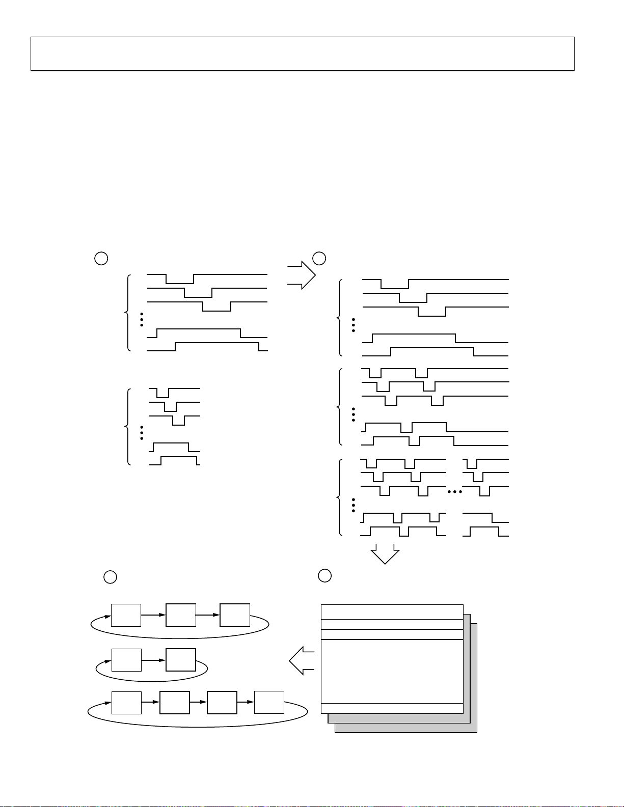
The AD9923A provides a very flexible solution for generating
vertical CCD timing; it can support multiple CCDs and different
system architectures. The 13-phase vertical transfer clocks, XV1 to
XV13, are used to shift lines of pixels into the horizontal output
register of the CCD. The AD9923A allows these outputs to be
individually programmed into various readout configurations,
using a four-step process as shown in Figure 35.
1. Use the vertical pattern group registers to create the individual
pulse patterns for XV1 to XV13.
2. Use the V-pattern groups to build the sequences and add more
information.
CREATE THE VERTICAL PATTERN GROUPS,
1
UP TO FOUR TOGGLE POSITIONS FOR EACH OUTPUT.
XV1
XV2
VPAT 0
XV3
XV11
XV12
V-SEQUENCE 0
(VPAT0, 1 REP)
3. Construct the readout for an entire field by dividing the field
into regions and assigning a sequence to each region. Each
field can contain up to nine regions to accommodate different
steps, such as high speed line shifts and unique vertical line
transfers, of the readout. The total number of V-patterns,
V-sequences, and fields are programmable and limited by the
number of registers. High speed line shifts and unique vertical
transfers are examples of the different steps required for
readout.
4. Use the MODE register to combine fields in any order for
various readout configurations.
BUILD THE V-SEQUENCES BY ADDING START POLARITY,
2
LINE START POSITION, NUMBER O F REPEATS, ALTERNATI ON
GROUP A/B INF ORMATIO N, AND HBLK/CLPOB PULSES.
XV1
XV2
XV3
XV11
XV12
XV1
XV2
VPAT 1
XV3
XV11
XV12
USE THE MODE REGISTER TO CONTRO L WHICH FI ELDS
4
ARE USED, AND IN WHAT ORDER (MAXIMUM OF SEVE N
FIELDS MAY BE COMBINED IN ANY ORDER).
FIELD 0
FIELD 3
FIELD 1 FIELD 2
FIELD 4
V-SEQUENCE 1
(VPAT1, 2 REP)
V-SEQUENCE 2
(VPAT1, N REP)
3
FIELD 0
XV1
XV2
XV3
XV11
XV12
XV1
XV2
XV3
XV11
XV12
BUILD EACH FIELD BY DIVIDI NG IT I NTO DIFF ERENT
REGIONS AND ASSIGNING A V-SEQUENCE TO EACH
(MAXIMUM OF NINE REGI ONS IN EACH FI ELD).
REGION 0: USE V-SEQUENCE 2
REGION 1: USE V-SEQUENCE 0
REGION 2: USE V-SEQUENCE 3
REGION 3: USE V-SEQUENCE 0
FIELD 5
FIELD 1 FIELD 4
Figure 35. Summary of Vertical Timing Generation
FIELD 2
REGION 4: USE V-SEQUENCE 2
FIELD 1
FIELD 2
05586-034
Rev. A | Page 24 of 84
AD9923A
X
Vertical Pattern (VPAT) Groups
A vertical pattern (VPAT) group defines the individual pulse
pattern for each XV1 to XV13 output signal. Tab le 1 5 summarizes
the registers that are available for generating each VPAT group.
The first, second, third, fourth, fifth, and sixth toggle positions
(XVTOG1, XVTOG2, XVTOG3, XVTOG4, XVTOG5,
XVTOG6) are the pixel locations where the pulse transitions. All
toggle positions are 13-bit values that can be placed anywhere in
the horizontal line.
More registers are included in the vertical sequence registers to
specify the output pulses: XV1POL to XV13POL specifies the
Table 15. Vertical Pattern Group Registers
Register Length (Bits) Range Description
XVTOG1 13 0 to 8191 pixel location First toggle position within line for each XV1 to XV12 output
XVTOG2 13 0 to 8191 pixel location Second toggle position
XVTOG3 13 0 to 8191 pixel location Third toggle position
XVTOG4 13 0 to 8191 pixel location Fourth toggle position
XVTOG5 13 0 to 8191 pixel location Fifth toggle position
XVTOG6 13 0 to 8191 pixel location Sixth toggle position
START POSITION OF VERTICAL PATTERN GROUP IS PROGRAMMABLE IN VERTICAL SEQUENCE REGISTERS.
start polarity for each signal, VSTART specifies the start
position of the VPAT group, and VLEN designates the total
length of the VPAT group, which determines the number of
pixels between each pattern repetition, if repetitions are used.
To achieve the best possible noise performance, ensure that
VSTART + VLEN < the end of the H-blank region.
Toggle positions programmed to either Pixel 0 or Pixel 8191 are
ignored. The toggle positions of unused XV-channels must be
programmed to either Pixel 0 or Pixel 8191. This prevents unpredictable behavior because the default values of the V-pattern
group registers are unknown.
HD
4
XV1
XV2
V12
PROGRAMMABLE SETTINGS:
1
START POLARITY (LOCATED IN V-SEQUENCE REGISTERS).
2
FIRST TOGGLE POSITION.
3
SECOND TOGGLE POSITION (A TOTAL OF SIX TOGGLE POSITIONS ALSO AVAILABLE FOR MORE COMPLEX PATTERNS).
4
TOTAL P ATTERN LENG TH FOR ALL VERTICAL OUTPUTS (LOCATED IN VERTICAL SEQUENCE REGIS TERS).
1
2
3
1
23
1
2
3
05586-035
Figure 36. Vertical Pattern Group Programmability
Rev. A | Page 25 of 84
AD9923A
X
Vertical Sequences (VSEQ)
A vertical sequence (VSEQ) is created by selecting one of the
V-pattern groups and adding repeats, a start position, and
horizontal clamping and blanking information. Each VSEQ is
programmed using the registers shown in Tab l e 1 6 . Figure 37
shows how each register is used to generate a V-sequence.
The VPATSELA and VPATSELB registers select the V-pattern
group that is used in a given V-sequence. Having two groups
available allows each vertical output to be mapped to a different
V-pattern group. The selected V-pattern group can have
repetitions added for high speed line shifts or line binning by
using the VREP registers for odd and even lines. Generally, the
same number of repetitions is programmed into both registers.
If a different number of repetitions is required on odd and even
lines, separate values can be used for each register (see the
1
HD
3
V1 TO XV13
V-PATTERN GROUP
44
VREP 2
Generating Line Alternation for V-Sequences and HBLK
section). The VSTARTA and VSTARTB registers specify the pixel
location where the V-pattern group starts. The VMASK register is
used in conjunction with the FREEZE/RESUME registers to enable
optional masking of the XV outputs. Either or both of the
FREEZE1/RESUME1 and FREEZE2/RESUME2 registers can be
enabled.
The line length (in pixels) is programmable using the HDLEN
registers. Each V-sequence can have a different line length to
accommodate various image readout techniques. The maximum
number of pixels per line is 8192. Note that the last line of the
field can be programmed separately using the HDLAST register,
located in the field register (see Ta ble 1 7).
2
VREP 3
CLPOB
PBLK
HBLK
PROGRAMMABLE SETTING S FOR EACH VERTICAL SEQ UENCE:
1
START POSI TION I N THE LINE OF SELECTED V-PATT ERN GROUP.
2
HD LINE LENG TH.
3
V-PATTERN SELECT (VPATSEL) TO SELECT ANY V-PATTERN GROUP.
4
NUMBER OF REPETITIONS OF THE V-PATTERN GROUP (IF NEEDED).
5
START POL ARITY AND TO GGLE POSITIO NS FOR CLP OB AND PBLK SIG NALS.
6
MASKING POLARITY AND TOGGLE POSITIONS FOR HBLK SIGNAL.
6
5
05586-036
Figure 37. V-Sequence Programmability
Rev. A | Page 26 of 84

AD9923A
Table 16. V-Sequence Registers1
Length
Register
HOLD 1 On/off Use in conjunction with VMASK. 1 = hold instead of FREEZE/RESUME.
VMASK 2 0 to 3 mask mode
0 = no mask.
1 = enable FREEZE1/RESUME1.
2 = enable FREEZE2/RESUME2.
3 = enable both FREEZE1/RESUME1 and FREEZE2/RESUME2.
HDLEN 13 0 to 8191 pixels HD line length in each V-sequence.
XV1POL to
XV13POL
GROUPSEL 12 1b for each XV output
0 = assigns to VPATSELA.
1 = assigns to VPATSELB.
TWO_GROUP 1 High/low When high, all XV outputs combine Group A and Group B.
VPATSELA 5 0 to 31 V-pattern number Selected V-pattern for Group A.
VPATSELB 5 0 to 31 V-pattern number Selected V-pattern for Group B. If SPVTP_ENABLE = 1, VPATSELB is used
VPATA_MODE 2 0 to 3 repetition mode Selects alternation repetition mode for Group A only.
0 = disable alternation, use VREPA_1 for all lines.
1 = 2-line. Alternate VREPA_1 and VREPA_2 (same as odd/even).
2 = 3-line. Alternate VREPA_1, VREPA_2, and VREPA_3.
3 = 4-line. Alternate VREPA_1, VREPA_2, VREPA_3, and VREPA_4.
VSTARTA 13 0 to 8191 pixel location Start position for the selected V-Pattern Group A.
VSTARTB 13 0 to 8191 pixel location Start position for the selected V-Pattern Group B. If SPVTP_ENABLE = 1,
VLENA 13 0 to 8191 pixels Length of selected V-Pattern Group A.
VLENB 13 0 to 8191 pixels Length of selected V-Pattern Group B.
VREPB_ODD 12 0 to 4095 repeats Number of repetitions for the V-Pattern Group B for odd lines.
VREPB_EVEN 12 0 to 4095 repeats Number of repetitions for the V-Pattern Group B for even lines.
VREPA_1 12 0 to 4095 repeats Number of repetitions for the V-Pattern Group A for first lines (odd).
VREPA_2 12 0 to 4095 repeats Number of repetitions for the V-Pattern Group A for second lines (even).
VREPA_3 12 0 to 4095 repeats Number of repetitions for the V-Pattern Group A for third lines.
VREPA_4 12 0 to 4095 repeats Number of repetitions for the V-Pattern Group A for fourth lines.
FREEZE1 13 0 to 8191 pixel location Pixel location where the XV outputs freeze or hold (see VMASK).
RESUME1 13 0 to 8191 pixel location Pixel location where the XV outputs resume operation (see VMASK).
FREEZE2 13 0 to 8191 pixel location Pixel location where the XV outputs freeze or hold (see VMASK).
RESUME2 13 0 to 8191 pixel location Pixel location where the XV outputs resume operation (see VMASK).
SPVTP_ACTLINE 12 0 to 4095 line location Active line for second VTP insertion.
SPVTP_ENABLE 1 High/low When high, second VTP is inserted into SPVTP_ACTLINE.
1
See Table 12 and Table 13 for CLPOB, PBLK, and HBLK registers.
(Bits)
Range Description
Enables the masking of XV1 to XV13 outputs at the locations specified by
the FREEZE/RESUME registers.
1 High/low Start polarity for each XV1 to XV13 output.
Assigns each XV1 to XV13 output to either V-Pattern Group A or
V-Pattern Group B.
for second VTP inserted in SPVTP_ACTLINE.
VSTARTB is used for start position of VPATSELB in SPVTP_ACTLINE.
If no alternation is required for Group B, set VREPB_ODD equal to
VREPB_EVEN.
If no alternation is required for Group B, set VREPB_EVEN equal to
VREPB_ODD.
Rev. A | Page 27 of 84

AD9923A
X
Group A/Group B Selection
The AD9923A has the flexibility to use two V-pattern groups in
a vertical sequence. In general, all vertical outputs use the same
V-pattern group during a sequence, but some outputs can be
assigned to a different V-pattern group. This is useful during
certain CCD readout modes.
The GROUPSEL register is used to select Group A or Group B
for each XV output (the LSB is XV1, the MSB is XV13). Setting
each bit to 0 selects Group A; setting each bit to 1 selects Group B.
If only a single V-pattern group is needed for the vertical
outputs, Group A is used by default (GROUPSEL = 0), and the
outputs use the V-pattern group specified by the VPATSELA
register.
HD
XV1 TO XV11 USE
V-PATTERN GROUP A
XV1
OPTIONAL HOLD AREA
If Group B flexibility is needed, the outputs set to 1 in the
GROUPSEL register use the V-pattern group selected by the
VPATSELB register. For example, Figure 38 shows outputs
XV12 and XV13 using a separate V-Pattern Group B to perform
special CCD timing.
Another application of the Group A and Group B registers is to
combine two VPAT groups for more complex patterns. This is
achieved by setting the TWO_GROUP register to 1. Figure 39
shows an example of this timing. When TWO_GROUP = 1,
the Group A and Group B toggle positions are both used. In
addition, length, starting polarity, and number of repetitions
are all determined by the appropriate registers for Group A
when TWO_GROUP = 1. Figure 40 shows the more complex
operation of combining Group A and Group B with repetition.
FOR GROUP A
XV11
XV12
XV13
XV1
XV13
HD
HD
XV12, XV13 USE
V-PATTERN GROUP B
V-PATTERN GROUP A
V-PATTERN
GROUP A
Figure 38. Using Separate Group A and Group B Patterns
V-PATTERN GROUP B
Figure 39. Combining Group A and Group B Patterns
V-PATTERN
GROUP B
05586-037
05586-038
XV1
V13
GROUP A REP 1 G ROUP A REP 2 GROUP A REP 3
Figure 40. Combining Group A and Group B Patterns, with Repetition
Rev. A | Page 28 of 84
06415-039

AD9923A
Generating Line Alternation for V-Sequences and HBLK
During low resolution readout, some CCDs require a different
number of vertical clocks on alternate lines. The AD9923A can
support such CCDs by using different VREP registers. This
allows a different number of VPAT repetitions to be programmed
on odd and even lines.
Note that only the number of repeats is different in odd and
even lines, but the VPAT group remains the same. There are
separate controls for the assigned Group A and Group B patterns.
Both Group A and Group B can support odd and even line
alternation. Group A uses the VREPA_1 and VREPA_2 registers; Group B uses the VREPB_ODD and VREPB_EVEN
registers. Group A can also support three-line and four-line
alternation by using the VREPA_3 and VREPA_4 registers.
Additionally, the HBLK signal can be alternated for odd and
even lines. When the HBLKALT = 1, the HBLKTOGE1 and
HBLKTOGE2 positions are used on odd lines, and the
HBLKTOGE3 to HBLKTOGE6 positions are used on even
lines. This allows the HBLK interval to be adjusted on odd
and even lines if needed.
Figure 41 shows an example of simultaneous VPAT repetition
alternation and HBLK alternation. Both types of alternation can
be used separately.
HD
XV1
XV2
XV13
HBLK
NOTES
1. THE NUMBER OF REPEATS FOR V-PATT ERN GROUP A O R GROUP B CAN BE ALT ERNATED ON O DD AND EVEN LINES.
2. GROUP A ALSO SUPPO RTS 3-LI NE AND 4-LINE AL TERNATIO N USING THE ADDI TIONAL VREPA_3 AND VREPA_4 REG ISTERS.
3. THE HBLK TOGGLE POSITIONS CAN ALSO BE ALTERNATE D BETWEEN ODD AND EVEN LINES T O GENERATE DIFFERENT HBLK PATTERNS
FOR ODD/E VEN LINES. SEE THE HORI ZONTAL CLAMPING AND BL ANKING SECTI ON FOR MO RE INFORMAT ION ON HBL K.
VREPA_1 = 2
(OR VREPB_ODD = 2)
HBLKTOGE1 HBLKTOG E2 HBLKTOGE3 HBL KTOGE4 HBLKTOGE1 HBL KTOGE2
Figure 41. Odd/Even Line Alternation of VPAT Repetitions and HBLK Toggle Positions
VREPA_2 = 5
(OR VREPB_EVEN = 5)
VREPA_1 = 2
(OR VREPB_ODD = 2)
05586-040
Rev. A | Page 29 of 84

AD9923A
X
Masking Using Freeze/Resume Registers
As shown in Figure 42 and Figure 43, the FREEZE/RESUME
registers are used to temporarily mask the XV outputs. The
pixel locations to start (FREEZE) and end (RESUME) the
masking create an area in which the vertical toggle positions are
ignored. At the pixel location specified in the FREEZE register,
the XV outputs are held static at their current dc state, high or
low. The XV outputs are held until the internal pixel counter
reaches the pixel location specified by the RESUME register, at
which point the signals continue with any remaining toggle
positions.
Two sets of FREEZE/RESUME registers are provided, allowing
the vertical outputs to be interrupted twice in the same line. The
FREEZE and RESUME positions are enabled using the VMASK
register.
It is not recommended to use FREEZE/RESUME at the same
time as the SWEEP function.
HD
XV1
V13
Figure 42. Not Using FREEZE/RESUME
HD
XV1
XV13
NOTES
1. ALL TOGGLE POSITIONS WITHIN THE FREEZE-RESUME MASKING AREA ARE IGNORED. H-COUNTER CONTINUES TO COUNT DURING MASKING .
2. TWO SEPARATE MASKI NG AREAS ARE AVAIL ABLE FO R EACH GROUP A, USING FREEZE1/RESUME1 AND FREEZE2/ RESUME2 REGI STERS.
Figure 43. Using FREEZE/RESUME
NO MASKING AREA
MASKING AREA
FREEZE RESUME
FOR GROUP A
5586-041
05586-042
Rev. A | Page 30 of 84

AD9923A
X
X
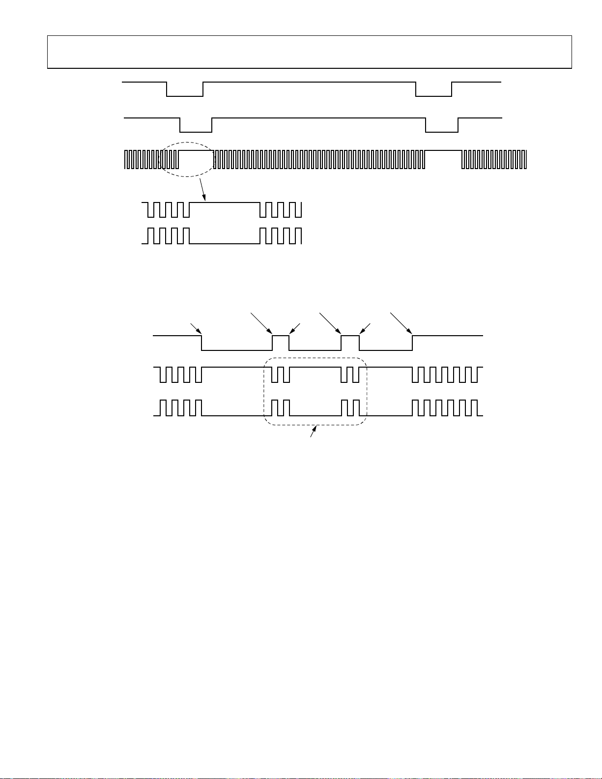
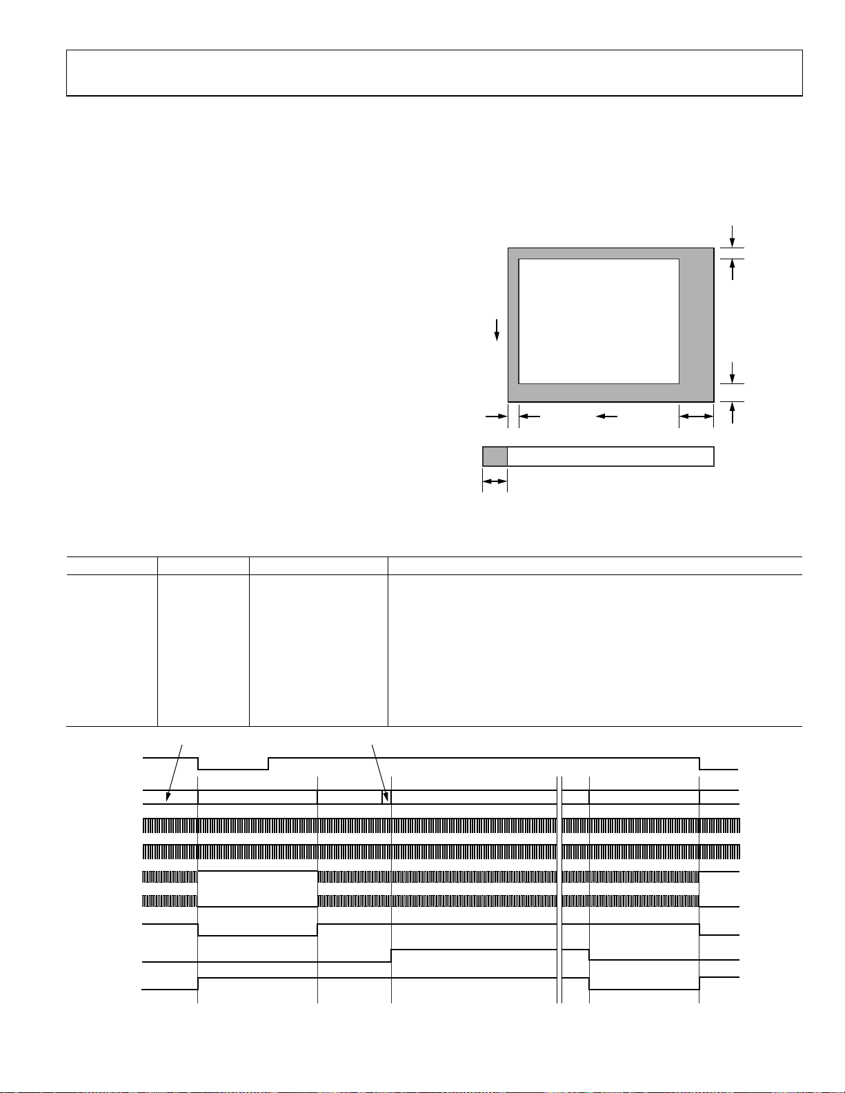
X
X
X
X
Hold Area Using FREEZE/RESUME Registers
The FREEZE/RESUME registers can also be used to create a
hold area, in which the XV outputs are temporarily held and
then later resume at the point where they were held. As shown
in Figure 44, this is different than using the VMASK register,
because the XV outputs continue from where they stopped (as
opposed to having the pixel counter run continuously), with
any toggle positions that fall between the FREEZE and
RESUME locations being ignored. Signals assigned to Group B
are not affected by the hold area.
HD
FREEZE RESUME
XV1
V11
V12
V13
NOTES
1. WHEN HOLD = 1 FOR ANY V-SEQUENCE, THE FREEZE AND RESUME REGISTERS ARE USED TO SPECIFY THE HOLD AREA FOR GROUP A.
2. ABOVE EXAMPLE: ALL XV-OUTPUTS ARE ASSIGNED TO GROUP A.
3. H-COUNTER F OR GROUP A (XV1 TO XV13) STOPS DURI NG HOLD AREA.
HOLD AREA
FOR GROUP A
Figure 44. Hold Area for Group A
HD
FREEZE
XV1
HOLD AREA
FOR GROUP A
RESUME
05586-043
V11
V12
NO HOLD
AREA FOR
V13
NOTES
1. ABOVE EXAMPLES: XV12 AND XV13 ARE ASSIGNED TO GROUP B.
2. GROUP B DOES NOT USE HOLD AREA.
Figure 45. Group B Does Not Use Hold Area
GROUP B
05586-044
Rev. A | Page 31 of 84

AD9923A
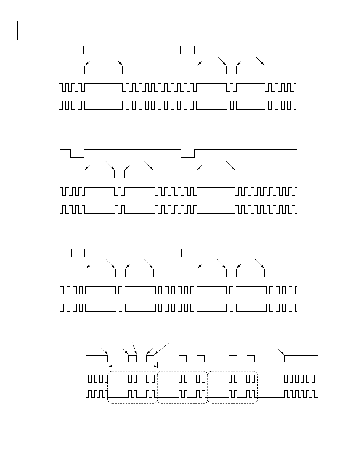
Complete Field: Combining V-Sequences
After the V-sequences are created, they are combined to create
different readout fields. A field consists of up to nine regions.
Within each region, a different V-sequence can be selected.
Figure 46 shows how the sequence change position (SCP)
registers designate the line boundary for each region and how
the VSEQSEL registers select the V-sequence for each region.
Registers to control the VSG outputs are also included in the
field registers. Table 1 7 summarizes the registers used to create
the different fields.
The VSEQSEL registers, one for each region, select which
V-sequences are active during each region. The SWEEP
registers can enable the sweep mode during any region.
The MULTI registers are used to enable the multiplier mode
during any region. The SCP registers create the line boundaries
for each region. The VDLEN register specifies the total number
of lines in the field. The total number of pixels per line (HDLEN)
is specified in the V-sequence registers, and the HDLAST
Table 17. Field Registers
Length
Register
VSEQSEL 5
SWEEP 1 High/low Enables sweep mode for each region when set high.
MULTI 1 High/low Enables multiplier mode for each region when set high.
SCP 12 0 to 4095 line number Sequence change position (SCP) for each region.
VDLEN 12 0 to 4095 lines Total number of lines in each field.
HDLAST 13 0 to 8191 pixels Length in pixels of the last HD line in each field.
VSTARTSECOND 13 0 to 8191 pixels Start position of the second V-pattern group applied during VSG line.
VPATSECOND 5
SGMASK 16 High/low, each VSG
[0] Masking for VSG1 on SGLINE1.
[1] Masking for VSG1 on SGLINE2.
[2] Masking for VSG2 on SGLINE1.
[3] Masking for VSG2 on SGLINE2.
[15] Masking for VSG8 on SGLINE1.
[16] Masking for VSG8 on SGLINE2.
SGPATSEL 24
SGACTLINE1 12 0 to 4095 line number Selects the line in the field where the VSG is active.
SGACTLINE2 12 0 to 4095 line number Selects a second line in the field to repeat the VSG signals.
(Bits) Range Description
0 to 31 V-sequence
number
0 to 31 V-pattern
group number
0 to 7 pattern
number, each VSG
Selected V-sequence for each region in the field.
Selected V-pattern group for the second pattern applied during VSG line.
Set high to mask each VSG output. Two bits for each VSG output: one for SGLINE1,
and one for SGLINE2.
Selects the VSG pattern number for each VSG output. VSG1[2:0], VSG2[5:3],
VSG3[8:6], VSG4[11:9], VSG5[14:12], VSG6[17:15], VSG7[20:18], VSG8[23:21].
register specifies the number of pixels in the last line of the
field. HDLEN, VDLEN, HDLAST registers are ignored when
the part is in slave mode. The VPATSECOND register is used to
add a second V-pattern group to the XV1 to X12 outputs during
the sensor gate (VSG) line.
The SGMASK register is used to enable or disable each VSG
output. There are two bits for each VSG output to enable
separate masking during SGACTLINE1 and SGACTLINE2.
Setting a masking bit high disables, or masks, the output; setting it
low enables the output. The SGPATSEL register assigns one of the
eight SG patterns to each VSG output. Each SG pattern is created
separately using the SG pattern registers. The SGACTLINE1
register specifies which line in the field contains the VSG
outputs. The optional SGACTLINE2 register allows the same
VSG pulses to repeat on a different line, although separate
masking is available for SGACTLINE1 and SGACTLINE2.
Rev. A | Page 32 of 84

AD9923A
XV1 TO XV13
SCP 0
VD
HD
VSEQSEL0 VSEQSEL1
VSG
FIELD SETTINGS:
1. SEQUENCE CHANG E POSIT IONS (SCP 1 TO SCP8) DEFINE EACH OF THE NINE AVAI LABLE REGIONS IN THE FIELD.
2. VSEQSEL0 TO VSEQSEL8 SELECTS THE DESIRED V-SEQUENCE FOR EACH REGION.
3. SGLI NE1 REGIST ER SELECTS WHICH HD LI NE IN THE FI ELD CONT AINS THE SENS OR-GATE P ULSE(S).
REGION 0
SCP 1 SCP 2
REGION 1 REGION 2 REGION 3 REGION 4 REGION 8
VSEQSEL2
SGACTLINE
Figure 46. Complete Field Is Divided into Regions
SCP 3
VSEQSEL3
Second V-Pattern Group During VSG Active Line and Special V-Pattern Insertion
Most CCDs require additional vertical timing during the sensor
gate line. The AD9923A can output a second V-pattern group
for XV1 to XV13 during the line when the VSG1 to VSG8
sensor gates are active. Figure 47 shows a typical VSG line,
which includes two sets of V-pattern groups for XV1 to XV13.
At the start of the VSG line, the V-pattern group is selected
using the appropriate VSEQSEL register. The second V-pattern
group, unique to the VSG line, is selected using the VPATSECOND
register, located in the field registers. The start position of the
second VPAT group uses the VSTARTSECOND register. For
more information, see Ta b le 17 .
SCP 4
VSEQSEL4
SCP 5
SCP 8
VSEQSEL8
Table 18. Special Second V-Pattern Insertion
Length
Register
(Bits)
Range Description
SPXV_EN 1 0 or 1
SPXV_ACT 12
Line 0 to
Line 4095
VPATSELB 5
0 to 31
V-pattern
number
VSTARTB 13
0 to 8191
pixel
location
05586-045
0 = off, 1= enable special
second V-pattern insertion.
Active line for special
second V-pattern insertion.
Selected V-pattern for
special second V-pattern
insertion if SPXV_EN = 1.
Start position for selected
V-pattern for special
second V-pattern
insertion if SPXV_EN = 1.
In addition to inserting a second V-pattern into the VSG line,
the AD9923A can insert a second V-pattern into any other
single line in each sequence. To enable this function in a particular sequence, set the SPXV_EN register in the appropriate
set of sequence registers to 1. The SPXV_ACT register determines
the active line for the special second V-pattern. The VPATSELB
and VSTARTB registers control both the V-pattern used and the
starting pixel location of the special second V-pattern. For more
information, see Table 1 8.
To avoid undesired behavior, do not use the special second
V-pattern in the VSG line; use the existing VPATSECOND and
VSTARTSECOND registers to insert a second V-pattern into
the VSG line. It is recommended that VPATSECOND and
VSTARTSECOND registers are used to create complex timing in
the sensor gate line and not the GROUPB registers. Additionally,
given that the special second V-pattern insertion uses some of the
Group B registers, the user cannot use the special second V-pattern
insertion function and Group B in the same sequence.
Sweep Mode Operation
The AD9923A contains an additional mode of vertical timing
operation called sweep mode. This mode is used to generate a
large number of repetitive pulses that span across multiple HD
lines. Normally, the vertical timing of the AD9923A must be
contained within one HD line length, but when sweep mode is
enabled, the HD boundaries are ignored until the region is
finished. This is useful, for example, in CCD readout operations.
Depending on the vertical resolution of the CCD, up to 3000 clock
cycles, spanning across several HD line lengths, can be required
to shift charge out of the vertical interline CCD registers. These
registers must be free of all charge at the end of the image
exposure before the image is transferred. This can be accomplished in sweep mode by quickly shifting out any charge using
a long series of pulses from the XV1 to XV13 outputs. To enable
sweep mode in any region, program the appropriate SWEEP
register to high.
Rev. A | Page 33 of 84

AD9923A
X
HD
VSG
XV1
XV2
V13
START POSI TION F OR SECOND VPAT GROUP
USES VSTARTS ECOND REGISTER
Figure 47. Example of Second VPAT Group During Sensor Gate Line
VD
HD
XV1 TO XV13
LINE 0 LINE 1
REGION 0 REGION 2
SCP 1 SCP 2
Figure 48. Example of Sweep Region for High Speed Vertical Shift
Figure 48 shows an example of sweep mode operation. The
number of required vertical pulses depends on the vertical
resolution of the CCD. The XV1 to XV13 output signals are
generated using the V-pattern registers (shown in Tab le 1 5 ).
A single pulse is created using the polarity and toggle position
registers. The number of repetitions is then programmed to
match the number of vertical shifts required by the CCD.
Repetitions are programmed in the V-sequence registers using
the VREP registers. This produces a pulse train of the appropriate
length. Normally, the pulse train is truncated at the end of the
HD line length, but with sweep mode enabled, the HD
boundaries are ignored. In Figure 48, the sweep region occupies
23 HD lines. After the sweep mode region is complete, normal
sequence operation resumes in the next region. When using
sweep mode, set the region boundaries, using the sequence
change position registers, to the appropriate lines to prevent the
sweep operation from overlapping with the next V-sequence.
Multiplier Mode
To generate very wide vertical timing pulses, a vertical region
can be configured into a multiplier region. This mode uses the
V-pattern registers in a slightly different manner. Multiplier mode
can be used to support unusual CCD timing requirements, such
as vertical pulses that are wider than the 13-bit V-pattern toggle
position counter.
SECOND VPAT GROUP
LINE 24 LINE 25LINE 2
REGION 1: SWEEP REGION
counter (HD counter) to specify the toggle position locations
(XVTOG1, XVTOG2, XVTOG3, XVTOG4, XVTOG5, and
XVTOG6) of the VPAT group, the VLEN value is multiplied by
the XVTOG value to allow very long pulses to be generated. To
calculate the exact toggle position, counted in pixels after the
start position, use the following equation:
Multiplier Mode Toggle Position = XVTOG × VLEN
Because the XVTOG value is multiplied by the VLEN value, the
resolution of the toggle position placement is reduced.
If VLEN = 4, the toggle position accuracy is reduced to four
pixel steps, instead of single pixel steps. Ta b le 1 9 summarizes
how the VPAT group registers are used in multiplier mode
operation. In multiplier mode, the VREP registers should be
programmed to the value of the highest toggle position.
The example shown in Figure 49 illustrates this operation. The
first toggle position is 2, and the second toggle position is 9. In
nonmultiplier mode, this causes the V-sequence to toggle at
Pixel 2 and Pixel 9 within a single HD line. However, in
multiplier mode the toggle positions are multiplied by
VLEN = 4; therefore, the first toggle occurs at pixel count = 8,
and the second toggle occurs at pixel count = 36. Sweep mode is
also enabled to allow the toggle positions to cross the HD line
boundaries.
05586-046
5586-047
The start polarity and toggle positions are used in the same
manner as the standard VPAT group programming, but the
VLEN register is used differently. Instead of using the pixel
Rev. A | Page 34 of 84
The MULTI function only applies to signals assigned to Group A.
It cannot be used at the same time as the TWOGROUP function or
if any signals are assigned to Group B.

AD9923A
Table 19. Multiplier Mode Register Parameters
Length
Register
MULTI 1 High/low High enables multiplier mode
XVPOL 1 High/low Starting polarity of XV1 to XV13 signals in each VPAT group
XVTOG 13 0 to 8191 pixel location Toggle positions for XV1 to XV13 signals in each VPAT group
VLEN 13 0 to 8191 pixels Used as multiplier factor for toggle position counter
VREP 12 0 to 4095 VREPE/VREPO should be set to the value of the highest XVTOG value
(Bits)
HD
Range Description
START POSITION OF VPAT GROUP IS STILL PROGRAMMED IN THE V-SEQUENCE REGISTERS
3
55
VLEN
PIXEL
NUMBER
XV1 TO XV13
1234123412341234123412341234123412341234
12345678910111213141516171819202122232425262728293031323334353637383940
4
1
MULTIPLIER MODE V-PATTERN GROUP PROPERTIES:
1
START POL ARITY (ABOVE: STARTPOL = 0).
2
FIRST AND SECOND TOGGLE POSITIONS (ABOVE: XVTOG1 = 2, XVTOG2 = 9).
3
LENGTH OF VPAT COUNTER (ABOVE: VPATLEN = 4); THIS IS THE MINIMUM RESOLUTION FOR TOGGLE POSITION CHANGES.
4
TOGGL E POSIT IONS OCCUR AT LOCATIO N EQUAL TO (XVTOG × VPATLEN).
5
IF SWEEP REGION I S ENABLED, T HE V-PULSES MAY ALSO CROSS THE HD BOUNDRIES , AS SHOWN ABO VE.
2
4
2
5586-048
Figure 49. Example of Multiplier Region for Wide Vertical Pulse Timing
Rev. A | Page 35 of 84

AD9923A
Vertical Sensor Gate (Shift Gate) Patterns
In an interline CCD, the vertical sensor gates (VSG) are used to
transfer the pixel charges from the light sensitive image area
into the light shielded vertical registers. From the light shielded
vertical registers, the image is then read line by line using the
XV1 to XV13 vertical transfer pulses in conjunction with the
high speed horizontal clocks.
Tabl e 20 summarizes the VSG pattern registers. The AD9923A
has eight VSG outputs, VSG1 to VSG8. Each output can be
assigned to one of eight programmed patterns by using the
SGPATSEL register. Each pattern is generated in a similar
manner as the V-pattern groups, with a programmable start
polarity (SGPOL), first toggle position (SGTOG1), and second
toggle position (SGTOG2). The active line where the VSG1 to
VSG8 pulses occur is programmable using the SGACTLINE1
Table 20. VSG Pattern Registers
1
Length
Register
(Bits) Range Description
SGPOL 1 High/low Sensor gate starting polarity for SG patterns 0 to 7.
SGTOG1 13
0 to 8191 pixel
First toggle position for SG patterns 0 to 7.
location
SGTOG2 13
0 to 8191 pixel
Second toggle position for SG patterns 0 to 7.
location
SGMASK_BYP 8
High/low for
each VSG
SGMASK Bypass. This register overrides the SGMASK values in each field register. One
bit for each output, where Bit[0] is for VSG1 output and Bit 7 is for VSG8 output.
0 = active.
1 = mask output.
SGMASK_BYP_EN 1 0 or 1 1: enables SGMASK bypass.
1
See field registers in Table 17.
and SGACTLINE2 registers. Additionally, any of the VSG1 to
VSG8 pulses can be individually disabled using the SGMASK
register. The individual masking allows all SG patterns to be
preprogrammed, and the appropriate pulses for each field can
be separately enabled. For maximum flexibility, the SGPATSEL,
SGMASK, and SGACTLINE registers are separately programmable
for each field. More detail is given in the Complete Field:
Combining V-Sequences section.
Additionally, there is the SGMASK_BYP register (Address 0x59)
that overrides SG masking in the field registers. The SGMASK_BYP
register allows sensor gate masking to be changed without
modifying the field register values. The SGMASK_BYP register
is SCK updated; therefore, the new SG-masking values update
immediately.
HD
VSG PATTERNS
VD
4
12 3
PROGRAMMABLE SETTING S FOR EACH PAT TERN:
1
START POL ARITY OF PULSE.
2
FIRST TOGGLE POSITION.
3
SECOND TOGGLE POSITION.
4
ACTIVE LI NE FOR VSG PULSES WI THIN THE F IELD (PRO GRAMMABLE I N THE FIELD REGIST ER, NOT F OR EACH PATTERN).
Figure 50. Vertical Sensor Gate Pulse Placement
Rev. A | Page 36 of 84
5586-049

AD9923A
MODE Register
The MODE register is a single register that selects the field timing
of the AD9923A. Typically, all field, V-sequence, and V-pattern
group information is programmed into the AD9923A at startup.
During operation, the MODE register allows the user to select
any combination of field timing to meet the current requirements
of the system. Using the MODE register in conjunction with
preprogrammed timing greatly reduces the system programming
requirements during camera operation. Only a few register writes
are required when the camera operating mode is changed rather
than having to rewrite the vertical timing information with each
camera mode change.
A basic still camera application can require five fields of vertical
timing—one for draft mode operation, one for autofocusing, and
three for still image readout. The register timing information for
the five fields is loaded at startup. Depending on how the camera
is being used, the MODE register selects which field timing is
active during camera operation.
Table 21. Mode Register Contents—VD Updated
Address (Binary)
Data Bits
Default Value Description
12b10_xx_xxxx_xxxx [37:0] 0 A11, A10 must be set to 0x10; remaining A9:A0 bits used for D37:D28
[37:35] Number of fields (maximum of seven)
[34:30] Selected field for Field 7
[29:25] Selected field for Field 5
[24:20] Selected field for Field 6
[19:15] Selected field for Field 4
[14:10] Selected field for Field 3
[9:5] Selected field for Field 2
[4:0] Selected field for Field 1
EXAMPLE 1:
TOTAL FIELDS = 3, FIRST FIELD = FIELD 0, SECOND FIELD = FIE LD 1, THIRD FIELD = FIELD 2
MODE REGI STER CONT ENTS = 0x9800000820
FIELD 0
FIELD 1 FIELD 2
Tabl e 21 shows how the MODE register bits are used. Unlike
other registers, the MODE register uses 10 address bits as data
bits to increase the total register size to 38 bits. The address
MSBs, A11 and A10, are 1 and 0, respectively, and are used to
specify the MODE register write. The three MSBs, D37, D36,
and D35 are used to specify the number of fields used. A value
from 1 to 7 can be selected using these three bits. The remaining
register bits are divided into five-bit sections to select which
programmed fields are used and in which order. Up to seven
fields can be used in a single MODE write. The AD9923A starts
with the field timing specified by the first field bit, and switches
to the timing specified by the second field bit on the next VD,
and so on.
After completing the number of fields specified in Bit D37 to
Bit D35, the timing generator of the AD9923A repeats itself by
starting at the first field. This continues until a new write to the
MODE register occurs. Figure 51 shows MODE register settings
for various field configurations.
EXAMPLE 2:
TOTAL FIELDS = 1, FIRST FIELD = FIELD 3
MODE REGI STER CONT ENTS = 0x8800000003
FIELD 3
EXAMPLE 3:
TOTAL F IELDS = 4, FIRST FIELD = FIELD 5, SECOND FIELD = FIE LD 1, THIRD F IELD = F IELD 4, F OURTH FI ELD = FI ELD 2
MODE REGI STER CONT ENTS = 0xA000011025
FIELD 5
FIELD 1 FIELD 4
Figure 51. Using the Mode Register to Select Field Timing
Rev. A | Page 37 of 84
FIELD 2
05586-050

AD9923A
VERTICAL TIMING EXAMPLE
To better understand how the AD9923A vertical timing
generation is used, consider the example CCD timing chart
in Figure 52. It illustrates a CCD using a general three-field
readout technique. As described in the Complete Field:
Combining V-Sequences section, each readout field should
be divided into separate regions to perform each step of the
readout. The sequence change position (SCP) registers determine the line boundaries for each region. Then, the VSEQSEL
registers assign a V-sequence to each region. Each V-sequence
contains specific timing information required for each region:
XV1 to XV6 pulses (using VPAT groups), HBLK/CLPOB timing,
and VSG patterns for the SG active lines.
The example shown in Figure 52 requires four regions, labeled
Region 0, Region 1, Region 2, and Region 3, for each of the
three fields. Because the AD9923A allows many individual
fields to be programmed, Field 0, Field 1, and Field 2 can be
created to meet the requirements of this timing example. In this
example, the four regions for each field are very similar, but the
individual registers for each field allow flexibility to accommodate
more complex timing requirements.
Region 0
Region 0 is a high speed vertical shift region. Sweep mode can
be used to generate this timing operation, with the desired
number of high speed vertical pulses needed to clear any charge
from the vertical registers of the CCD.
Region 1
Region 1 consists of two lines and uses standard, single line,
vertical shift timing. The timing of this region is the same as the
timing of Region 3.
Region 2
Region 2 is the sensor gate line, where the VSG pulses transfer
the image into the vertical CCD registers. This region might
require use of the second V-pattern group for the SG active line.
Region 3
Region 3 also uses the standard, single line, vertical shift timing,
the same timing used in Region 1. In summary, four regions are
required in each of the three fields.
The timing for Region 1 and Region 3 is essentially the same,
reducing the complexity of the register programming. Other
registers, such as the MODE register, shutter control registers
(that is, TRIGGER, and the registers to control the SUBCK,
VSUB, MSHUT, and STROBE outputs), and the AFE gain
registers, VGAGAIN and CDSGAIN, must be used during the
readout operation. These registers are explained in the MODE
Register and Variable Gain Amplifier sections.
Rev. A | Page 38 of 84

AD9923A
05586-051
OPEN
N
N–3
21
18
15
12
9
6
3
REGION 1 REGION 2
REGIO N 0 REG ION 3
THIRD FIELD READOUT
N–1
N–4
20
17
14
11
8
5
2
FIELD 1 FIELD 2
REGION 1 REGION 2
REGION 0 REGION 3
SECOND FIEL D READOUT
N–2
N–5
16
13
10
7
4
1
FIELD 0
REGION 1 REGION 2
REGION 0 REGION 3
) FIRST FIELD READO UT
EXP
EXPOSURE (t
CLOSED
OPEN
VD
HD
XV1
XV3
XV2
XV4
XV5
XV6
SUBCK
MSHUT
VSUB
CCD
OUT
Figure 52. CCD Timing Example—Dividing Each Field into Regions
Rev. A | Page 39 of 84

AD9923A
VERTICAL DRIVER SIGNAL CONFIGURATION
As shown in Figure 53, XV1 to XV13, VSG1 to VSG8, and
XSUBCK are outputs from the internal AD9923A timing
generator, and V1 to V13 and SUBCK are the resulting outputs
from the AD9923A vertical driver. When VDR_EN = high, the
vertical driver mixes the XV and VSG pulses and amplifies
them to the high voltages required for driving the CCD. Tab le 2 2
through Tab le 3 7 describe the output polarities for these signals
vs. their input levels. Refer to these tables when determining the
register settings for the desired output levels. Note that when
VDR_EN = low, V1 to V13 are forced to VM and SUBCK is
forced to VLL. The VDR_EN pin takes priority over the XV and
VSG signals coming from the timing generator.
The VDR_EN pin can be driven either with an external 3 V
logic signal or by one of the AD9923A shutter outputs
(MSHUT, VSUB, STROBE). To make the AD9923A compatible
with existing AD9923 designs, drive the VDR_EN pin with a
diode to either an external 3 V logic signal or to one of the
shutter outputs.
AD9923A
INTERNAL
TIMING
GENERATOR
XV1
VSG1
XV11
VSG2
XV3
VSG3
XV12
VSG4
VSG5
XV5
VSG6
VSG7
XV7
VSG8
XV2
XV4
XV6
XV8
XV9
XV10
XV13
XSUBCK
XSUBCNT
V-DRIVER
3V VH VL
V1
V11
V3
3-LEVEL OUTPUTS
V12
V5A
V5B
V7A
V7B
V2
V4
V6
V8
2-LEVEL OUTPUTS
V9
V10
V13
SUBCK
VDR_EN
05586-052
Figure 53. Internal Vertical Driver Input Signals
Rev. A | Page 40 of 84

AD9923A
Table 22. V1 Output Polarity
Vertical Driver Input
XV1 VSG1
L L VH
L H VM
H L VL
H H VL
V1 Output
Table 28. V11 Output Polarity
Vertical Driver Input
XV11 VSG2
L L VH
L H VM
H L VL
H H VL
V11 Output
Table 23. V3 Output Polarity
Vertical Driver Input
V3 Output XV3 VSG3
L L VH
L H VM
H L VL
H H VL
Table 24. V5A Output Polarity
Vertical Driver Input
V5A Output XV5 VSG5
L L VH
L H VM
H L VL
H H VL
Table 25. V5B Output Polarity
Vertical Driver Input
XV5 VSG6
L L VH
L H VM
H L VL
H H VL
V5B Output
Table 29. V12 Output Polarity
Vertical Driver Input
V12 Output XV12 VSG4
L L VH
L H VM
H L VL
H H VL
Table 30. V2 Output Polarity
Vertical Driver Input XV2 V2 Output
L VM
H VL
Table 31. V4 Output Polarity
Vertical Driver Input XV4 V4 Output
L VM
H VL
Table 32. V6 Output Polarity
Vertical Driver Input XV6 V6 Output
L VM
H VL
Table 26. V7A Output Polarity
Vertical Driver Input
XV7 VSG7
L L VH
L H VM
H L VL
H H VL
V7A Output
Table 27. V7B Output Polarity
Vertical Driver Input
XV7 VSG8
L L VH
L H VM
H L VL
H H VL
V7B Output
Table 33. V8 Output Polarity
Vertical Driver Input XV8 V8 Output
L VM
H VL
Table 34. V9 Output Polarity
Vertical Driver Input XV9 V9 Output
L VM
H VL
Rev. A | Page 41 of 84

AD9923A
V
Table 35. V10 Output Polarity
Vertical Driver Input XV10 V10 Output
L VM
H VL
Table 36. V13 Output Polarity
Vertical Driver Input XV13 V13 Output
L VM
H VL
XV1
VSG1
VH
1
VM
VL
Table 37. SUBCK Output Polarity
Vertical Driver Input
L L VH
L H VH
H L VMM
H H VLL
Figure 54. XV1, VSG1, and V1 Output Polarities
SUBCK Output XSUBCK XSUBCNT
05586-053
XV11
VSG2
VH
V11
VM
VL
05586-054
Figure 55. XV11, VSG2, and V11 Output Polarities
XV3
VSG3
VH
V3
VM
VL
Figure 56. XV3, VSG3, and V3 Output Polarities
05586-055
Rev. A | Page 42 of 84

AD9923A
V
V7A
XV12
VSG4
VH
V12
VM
VL
05586-056
Figure 57. XV12, VSG4, and V12 Output Polarities
XV5
VSG5
VH
V5A
VM
VL
05586-057
Figure 58. XV5, VSG5, and V5A Output Polarities
XV5
VSG6
VH
5B
VM
VL
05586-058
Figure 59. XV5, VSG6, and V5B Output Polarities
XV7
VSG7
VH
VM
VL
Figure 60. XV7, VSG7, and V7A Output Polarities
Rev. A | Page 43 of 84
05586-059

AD9923A
V
XV7
VSG8
VH
7B
VM
XV2, XV4, XV6, XV8
XV9, XV10, XV13
V2, V4, V6, V8
V9, V10, V13
XSUBCNT
SUBCK
VL
XSUBCK
VMM
VLL
VH
VM
Figure 61. XV7, VSG8, and V7B Output Polarities
VL
Figure 62. XV2, XV4, XV6, XV8, XV9, XV10, XV13 and V2, V4, V6, V8, V9, V10, V13 Output Polarities
Figure 63. XSUBCNT, XSUBCK, and SUBCK Output Polarities
05586-060
5586-061
05586-062
SHUTTER TIMING CONTROL
The CCD image exposure time is controlled by the substrate clock
signal (SUBCK) that pulses the CCD substrate to clear out
accumulated charge. The AD9923A supports three types of
electronic shuttering: normal, high precision, and low speed.
Together with the SUBCK pulse placement, the AD9923A can
accommodate different readout configurations to further
suppress the SUBCK pulses during multiple field readouts. The
AD9923A also provides programmable outputs to control an
external mechanical shutter (MSHUT), strobe/flash (STROBE),
and CCD bias select signal (VSUB). Up to four general shutter
pulses (SHUT0 to SHUT3) and two VSUB pulses (VSUB0 and
VSUB1) can be programmed and assigned to any of the three
shutter output pins. The user can also combine the following
Rev. A | Page 44 of 84
shutter and VSUB pulses with a logic XOR operation (symbolized
by ^) to generate more complex timing (up to four toggle positions per line) for MSHUT, STROBE and VSUB: SHUT0 ^ VSUB0,
SHUT0 ^ VSUB1, SHUT0 ^ SHUT1, and SHUT0 ^ SHUT2.
SUBCK: Three-Level Output
The AD9923A supports a three-level output from the SUBCK
buffer: VH, VMM, and VLL. The VH power supply is shared
with the V-driver outputs, but VMM and VLL are dedicated
mid and low supplies for the SUBCK buffer. There are two inputs to the SUBCK buffer, XSUBCK and XSUBCNT. XSUBCNT
is created by an internal multiplexer that selects from XV1 to
XV13, VSG1 to VSG8, MSHUT, STROBE, VSUB, SHUT0 to
SHUT3, FG_TRIG, high and low.

AD9923A
Table 38. XSUBCNT Multiplexer
Length
Register
XSUBCNT_MUX 5 0 to 31
0: XV6
1: XV8
2: XV9
3: XV10
4: VSG5
5: VSG6
6: VSG7
7: VSG8
8: VSG2
9: VSG3
10: VSG4
11: VSG1
12: XV13
13: VSUB
14: MSHUT
15: STROBE
16: XV1
17: XV2
18: XV3
19: XV4
20: XV5
21: XV7
22: XV11
23: XV12
24: SHUT0
25: SHUT1
26: SHUT2
27: SHUT3
28: FG_TRIG
29: invalid setting
30: high
31: low
(Bits)
Range Description
Selects internal signal to
be used for XSUBCNT
SUBCK: Normal Operation
By default, the AD9923A operates in a normal SUBCK configuration with the SUBCK signal pulsing in every VD field (see
Figure 64). The SUBCK pulse occurs once per line, and the total
number of repetitions within the field determines the exposure
time. The SUBCK pulse polarity and toggle positions within a
line are programmable, using the SUBCKPOL and SUBCK1TOG
registers (see Ta b le 3 9 ). The number of SUBCK pulses per field
is programmed in the SUBCKNUM register (Address 0x64).
As shown in Figure 64, the SUBCK pulses always begin in the
line following the SG active line (specified in the SGACTLINE
registers for each field). The SUBCKPOL, SUBCK1TOG,
SUBCK2TOG, SUBCKNUM, and SUBCKSUPPRESS registers
are updated at the start of the line after the sensor gate line, as
described in the Updating New Register Values section.
SUBCK: High Precision Operation
High precision shuttering is used in the same manner as normal
shuttering, but an additional register is used to control the last
SUBCK pulse. In this mode, the SUBCK pulses once per line,
but the last SUBCK in the field has an additional SUBCK pulse,
whose location is determined by the SUBCK2TOGx registers,
as shown in Figure 65. Finer resolution of the exposure time is
possible using this mode. Leaving the SUBCK2TOGx registers
set to their maximum value (0xFFFFFF) disables the last
SUBCK pulse (default setting).
SUBCK: Low Speed Operation
Normal and high precision shutter operations are used when
the exposure time is less than one field long. For exposure times
longer than one field interval, low speed shutter operation is
used. The AD9923A uses a separate exposure counter to
achieve long exposure times. The number of fields for the low
speed shutter operation is specified in the EXPOSURENUM
register (Address 0x63). As shown in Figure 66, this shutter
mode suppresses the SUBCK and VSG outputs from 0 fields up
to 4095 fields (VD periods). The VD and HD outputs can be
suppressed during the exposure period by programming the
VDHDOFF register to 1.
To generate a low speed shutter operation, trigger a long exposure by writing to the TRIGGER register, Bit D3. When this
bit is set high, the AD9923A begins an exposure operation at
the next VD edge. If a value greater than 0 is specified in the
EXPOSURENUM register, the AD9923A suppresses the
SUBCK output on subsequent fields.
If the exposure is generated using the TRIGGER register and
the EXPOSURENUM register is set to 0, the behavior of the
SUBCK is the same as during normal shutter or high precision
shutter operations, in which the TRIGGER register is not used.
Rev. A | Page 45 of 84

AD9923A
S
VD
HD
VSG
SUBCK
SUBCK PROGRAMMABLE SETTING S:
1. PULSE POLARITY USING THE SUBCKPOL REGISTER.
2. NUMBER OF PULSES WI THIN THE F IELD USI NG THE SUBCKNUM REG ISTER (SUBNUM = 3 IN THE ABOV E EXAMPLE).
3. PIXEL LOCATIO N OF PULSE WITHI N THE LINE AND PULSE WI DTH PROGRAMMED USING T HE SUBCK1TOG REG ISTER.
t
EXP
t
EXP
05586-063
Figure 64. Normal Shutter Mode
VD
HD
VSG
SUBCK
NOTES
1. SECOND SUBCK PULSE IS ADDED IN T HE LAST SUBCK LINE.
2. LOCATI ON OF SECOND PULSE I S FULLY PROGRAMMABLE USING THE SUBCK2TOG REG ISTER.
t
EXP
t
EXP
5586-064
Figure 65. High Precision Shutter Mode
TRIGGER
EXPOSURE
VD
VSG
t
EXP
UBCK
NOTES
1. SUBCK CAN BE SUPPRESSED FOR MULT IPLE F IELDS BY P ROGRAMMING THE EXPO SURE REGISTER TO BE G REATER THAN 0.
2. ABOVE EXAMPLE USES EXPOSURE = 1.
3. TRIGGER REGISTER MUST ALSO BE USED TO START THE LOW SPEED EXPOSURE.
4. VD/HD OUTPUTS CAN ALSO BE SUPPRESSED US ING THE VDHDOFF REGISTER = 1.
05586-065
Figure 66. Low Speed Shutter Mode Using EXPOSURE Register
Rev. A | Page 46 of 84

AD9923A
SUBCK: Suppression
Normally, the SUBCK begins pulsing on the line following the
sensor gate line (VSG). Some CCDs require suppressing the
SUBCK pulse for one or more lines following the VSG line. The
SUBCKSUPPRESS register enables such suppression.
Readout After Exposure
After the exposure, the readout of the CCD data occurs, beginning
with the sensor gate (VSG) operation. By default, the AD9923A
generates VSG pulses in every field. When only a single exposure
and readout frame are needed, as is the case in the CCD preview
mode, the VSG and SUBCK pulses can operate in every field.
However, often during readout, the SUBCK output must be
suppressed until the readout is complete. The READOUTNUM
register specifies the number of additional fields after the exposure
to continue the suppression of SUBCK. READOUTNUM can be
programmed for 0 to 7 fields, and should be preprogrammed at
startup, not at the same time as the exposure write. A typical
interlaced CCD frame readout mode generally requires two fields
of SUBCK suppression (READOUTNUM = 2) during readout.
A three-field, six-phase CCD requires three fields of SUBCK
suppression after the readout begins (READOUTNUM = 3).
If SUBCK output is required to initiate backup during the last field
of readout, program the READOUTNUM register to one less
than the total number of CCD readout fields. Similar to the
exposure operation, the readout operation must be triggered
using the TRIGGER register.
SUBCK: Additional Masking
The SUBCKMASK register (Address 0x65) allows more complex
SUBCK masking. If SUBCKMASK = 1, it starts masking the
SUBCK at the next VD edge. If SUBCKMASK = 2, it enables
users to select the internal SHUT3 signal and create a custom
SUBCK masking pattern that spans several fields.
When generating an exposure by using the TRIGGER register,
as previously described in the Readout After Exposure section,
the AD9923A outputs the SUBCK and VSG signals on every
field by default. This works well for continuous, single field
exposure and readout operations, such as those in the CCD live
preview mode. However, if the CCD requires a longer exposure
time, or if multiple readout fields are needed, the TRIGGER
register is needed to initiate specific exposure and readout
sequences.
Typically, the exposure and readout bits in the TRIGGER register
are used together. This initiates a complete exposure-plus-readout
operation. After the exposure, the readout occurs automatically.
The values in the EXPOSURE and READOUTNUM registers
determine the length of each operation.
It is possible to independently trigger the readout operation
without triggering the exposure operation. This causes the readout
to occur at the next VD, and the SUBCK output is suppressed
according to the value set in the READOUTNUM register.
The TRIGGER register also controls the SHUT and VSUB signals.
Each signal is individually controlled but dependent on the
triggering of the exposure and readout operations. See Figure 71
for a complete example of triggering the exposure and readout
operations.
Alternatively, it is possible to manually control the exposure and
readout operations by carefully updating the SUBCKSUPPRESS
and VSG masking registers upon every VD field. As described in
the following sections, it is possible to have partial or full manual
control of the shutter signals. This allows greater flexibility in
generating custom exposure/readout/shutter signal timing.
Rev. A | Page 47 of 84

AD9923A
Table 39. SUBCK and TRIGGER Register Parameters
Length
Register
TRIGGER 8 On/off for eight signals 0: triggers SHUT0 signal.
1: triggers SHUT1 signal.
2: triggers SHUT2 signal.
3: triggers SHUT3 signal.
4: triggers VSUB0 signal.
5: triggers VSUB1 signal.
6: triggers EXPOSURE operation.
7: triggers READOUT operation.
READOUTNUM 3 0 to 7 fields Number of fields to suppress SUBCK after exposure.
EXPOSURENUM 12 0 to 4095 fields
VDHDOFF 1 On/off Disable VD/HD output during exposure.
1 = disable VD.
0 = enable VD.
SUBCKPOL1 1 High/low SUBCK start polarity for SUBCK1 and SUBCK2.
SUBCK1TOG11 12 0 to 4095 pixel locations First toggle positions for first SUBCK pulse (normal shutter).
SUBCK1TOG2
SUBCK2TOG11 12 0 to 4095 pixel locations First toggle positions for second SUBCK pulse in last line (high precision).
SUBCK2TOG21 12 0 to 4095 pixel locations Second toggle positions for second SUBCK pulse in last line (high precision).
SUBCKNUM
1
12 1 to 4095 pulses Total number of SUBCKs per field, at one pulse per line.
SUBCKSUPPRESS1 12 0 to 4095 pulses Number of pulses, after the VSG line, to suppress SUBCK.
SUBCKMASK1 2 0 to 3 masking mode Additional masking of SUBCK output.
0 = no additional mask.
1 = start mask at VD edge.
2 = use internal SHUT3 signal to mask.
1
Register is not VD updated but updated at the start of the line after the sensor gate line.
Shutter Outputs
The AD9923A contains three shutter output pins: VSUB,
MSHUT, and STROBE. Internally, there are six possible shutter
signals available: VSUB0, VSUB1, SHUT0, SHUT1, SHUT2,
and SHUT3. Any of these signals, and the following combinations:
SHUT0 ^ VSUB0, SHUT0 ^ VSUB1, SHUT0 ^ SHUT1,
SHUT0 ^ SHUT2, can be mapped to any of the output pins
using the VSUB_CTRL, MSHUT_CTRL, and STROBE_CTRL
registers.
The VSUB signals behave differently than the SHUT signals,
and are generally used for the VSUB output pin. If a more generic
approach is desired for the shutter signals, the SHUT signals can
be used for the VSUB output pin.
It is also possible to configure the SYNC pin as an output and
send one of the internal shutter signals, or the combinations listed
above, to the SYNC pin using the TESTO_CTRL register
function. This provides the flexibility of outputting up to four
shutter outputs if the external SYNC input function is not needed.
(Bits)
Range Description
Number of fields to suppress to SUBCK and VSG during exposure time (low
speed shutter).
1
12 0 to 4095 pixel locations Second toggle positions for first SUBCK pulse (normal shutter).
VSUB Signal Operation
The CCD readout bias (VSUB) can be programmed to accommodate different CCDs. Figure 67 shows two available modes.
In Mode 0, VSUB goes active when the exposure begins during
the field of the last SUBCK. The on position (rising edge in
Figure 67) is programmable to any line within the field. VSUB
remains active until the end of the image readout. In Mode 1,
the VSUB is not activated until the start of the readout.
A function called VSUB_KEEPON is also available. When the
appropriate VSUB_KEEPON bit is set high, the VSUB output
remains active, even after the readout has finished. To disable
the VSUB at a later time, return this bit to low.
The AD9923A contains two programmable VSUB signals,
VSUB0 and VSUB1. Either of these signals can be mapped to
the VSUB output pin, the MSHUT pin, or the STROBE pin.
SHUT Signal Operation
SHUT signal operation is shown in Figure 68 through Figure 71.
Rev. A | Page 48 of 84

AD9923A
Tabl e 40 shows the register parameters for controlling the
SHUT signals. There are three different ways to use the SHUT
signals: automatic trigger, single trigger, and manual control.
Automatic Trigger
Generally, SHUT signals are triggered together with an exposure or readout operation, using the TRIGGER register. The
SHUT_ON and SHUT_OFF positions are fully programmable
to anywhere within the exposure period, using the field
(SHUT_ON_FD/SHUT_OFF_FD), line
(SHUT_ON_LN/SHUT_OFF_LN), and pixel
(SHUT_ON_PX/SHUT_OFF_PX) registers.
The field registers define the field in which the line and pixel
values are used, with respect to the value of the exposure counter.
The on and off positions can occur as soon as the field contains
the last SUBCK (Exposure Field 0), or as late as the final exposure
field before the readout begins. Separate field registers allow the
on and off positions to occur in different exposure fields.
Single Trigger
SHUT signals can be triggered without triggering an exposure
or readout operation. In this case, SHUT signals are triggered
using the TRIGGER register, but the exposure bit is not triggered.
Both the SHUT on and off positions occur in the next field, and
the SHUT_ON_FD/SHUT_OFF_FD register values are ignored.
Single trigger operation is useful if a pulse is required immediately in the next field without the occurrence of an exposure or
readout operation. Also, single trigger operation is useful when
the exposure or readout operation is manually generated without
using the TRIGGER register, and the SUBCK and VSG masking
are manually controlled.
Note that single trigger operation cannot occur if an exposure
operation has been triggered. SHUT signals behave in automatic
TRIGGER
VSUB
trigger mode if they, and an exposure operation, have been
triggered.
Manual Control
Any SHUT signal can be controlled in manual control mode,
instead of using the TRIGGER register to activate it. In this
mode, the individual on and off lines and pixel positions are
used separately, depending on the status of the manual signal
control register. Note that only a single toggle position, either
off or on, can be used in a VD interval.
As with single trigger operation, when manual control is
enabled, the SHUT_ON_FD/SHUT_OFF_FD register values
are ignored.
Because there is a separate bit to enable manual control on
SHUT signals, this operation can be used regardless of the
status of a triggered exposure operation.
Note that manual control can be used in conjunction with
automatic or single trigger operations. If a SHUT signal is turned
on using manual control, and then manual control is disabled,
the SHUT signal remains on. If a subsequent trigger operation
occurs, the on position toggle is ignored, because the signal is
already on. In this case, only the off position can be triggered.
Note that the trigger mechanism for the SHUT signals on the
AD9923A is different from the AD9923. On the AD9923, the
trigger signals are updated on the UPDATE line (Register 0x18)
in the field in which the TRIGGER register (Register 0x61) is
written to. If the trigger bit for a SHUT signal is deactivated in a
given field, this would cause any toggle positions for that SHUT
signal that occur after the UPDATE line to be ignored. In the
AD9923A, the internal trigger signals remain active for the
entire line following a write to the trigger register. In this case,
any toggle locations that are programmed after the UPDATE
line is processed.
VD
VSG1
t
EXP
SUBCK
2
VSUB
1
VSUB OPERATI ON:
1
ACTIVE POLARITY IS DEFINED BY VSUBPOL (ABOVE EXAMPLE IS VSUB ACTIVE HIGH).
2
ON POSIT ION IS PROGRAMMABLE , MODE 0 T URNS ON AT THE S TART OF E XPOSURE, MODE 1 TURNS O N AT THE START OF READOUT .
3
OFF POSITIO N OCCURS AT END OF READOUT.
4
OPTIO NAL VSUB KEEP-ON MODE LEAVES THE VSUB ACTIVE AT THE END O F THE READOUT .
MODE 0
MODE 1
Figure 67. VSUB0, VSUB1 Signal Programmability
2
READOUT
4
3
05586-066
Rev. A | Page 49 of 84

AD9923A
R
R
VD
VSG
SHUT0 TO SHUT3
1
OFF STATE
SHUT PROGRAMMABLE SETTINGS:
1
ACTIVE POLARITY. DEFINES T HE LOGIC LEVEL DURING ON TIME. ABOVE EXAMPLE USES ACT IVE POL ARITY = 1.
2
ON POSITION IS PROGRAMMABLE TO ANY LINE/PIXEL IN FIELD IMMEDIATELY FOLLOWING SINGLE TRIGGER WRITE.
3
OFF POSITIO N IS PROGRAMMABLE TO ANY L INE/PI XEL IN FI ELD IMME DIATELY F OLLO WING SI NGLE TRI GGER WRITE.
SINGLE TRIGGER
WRITE
ON STATE
2
3
5586-067
Figure 68. SHUT0 to SHUT3 Signal Programmability
TRIGGE
EXPOSURE
SHUT_ON = 0
(OFF)
EXPOSURE FI ELD 0 EX POSURE FI ELD 1 EXPOSURE FIEL D 2
t
EXP
VSG
SUBCK
SHUT_ON = 1
(ON)
VD
SHUT0 TO SHUT3
SUBCK
SHUT0 TO SHUT3
ON STATE
1
OFF STATE
SHUT PROGRAMMABLE SETTINGS:
1
ACTIVE POLARITY. DEFINES THE LOGIC LEVEL DURING ON TIME. ABOVE EXAMPLE USES ACTIVE POLARITY = 1.
2
ON POSIT ION IS PROGRAMMABLE DURING ANY EXPO SURE FIELD. ABOVE E XAMPLE USES SHUTON_FD = 1.
3
OFF PO SITIO N IS PROG RAMMABLE DURING ANY EXPOSURE FIELD. ABO VE EXAMPLE USES SHUTOF F_FD = 2.
2 3
Figure 69. Manual Control of SHUT0 to SHUT3 Signals
TRIGGE
EXPOSURE
AND SHUT
VD
VSG
1
OFF STATE
SHUT PROGRAMMABLE SETTINGS:
1
ACTIVE POLARITY. DEFINES T HE LOGIC LEVEL DURING ON TIME. ABOVE EXAMPLE USES ACT IVE POL ARITY = 1.
2
ON POSITION IS PROGRAMMABLE DURING ANY EXPOSURE FIELD. ABOVE EXAMPLE USES SHUTON_FD = 1.
3
OFF PO SITIO N IS PROG RAMMABLE DURING ANY EXPOSURE FIELD. ABOV E EXAMPLE US ES SHUTOF F_FD = 2.
EXPOSURE FI ELD 0 EXPOSURE FIE LD 1 EXPOSURE FIELD 2
t
EXP
ON STATE
2
Figure 70. Single Trigger Control of SHUT0 to SHUT3 Signals
05586-068
3
05586-011
Rev. A | Page 50 of 84

AD9923A
Table 40. VSUB0 to VSUB1 and SHUT0 to SHUT3 Register Parameters
Register Length (Bits) Range Description
VSUB_CTRL 3 0 to 7 Selects which internal shutter signal is mapped to the VSUB pin.
0: SHUT0.
1: SHUT1.
2: SHUT2.
3: SHUT3.
4: use VSUB0_MUX output.
5: use VSUB1_MUX output.
6: invalid setting.
7: use SHUT1_SHUT2_MUX output.
MSHUT_CTRL 3 0 to 7 Selects which internal shutter signal is mapped to the MSHUT pin.
0: SHUT0.
1: SHUT1.
2: SHUT2.
3: SHUT3.
4: use VSUB0_MUX output.
5: use VSUB1_MUX output.
6: invalid setting.
7: use SHUT1_SHUT2_MUX output.
STROBE_CTRL 3 0 to 7 Selects which internal shutter signal is mapped to the STROBE pin.
0: SHUT0.
1: SHUT1.
2: SHUT2.
3: SHUT3.
4: use VSUB0_MUX output.
5: use VSUB1_MUX output.
6: invalid setting.
7: use SHUT1_SHUT2_MUX output.
TESTO_CTRL 3 0 to 7 Selects which internal shutter signal is mapped to the TEST0 signal.
0: SHUT0.
1: SHUT1.
2: SHUT2.
3: SHUT3.
4: use VSUB0_MUX output.
5: use VSUB1_MUX output.
6: invalid setting.
7: use SHUT1_SHUT2_MUX output.
VSUB0_MUX 1 High/low 0 = use VSUB0.
1 = use SHUT0 ^ VSUB0.
VSUB1_MUX 1 High/low 0 = use VSUB1.
1 = use SHUT0 ^ VSUB 1.
SHUT1_SHUT2_MUX 1 High/low 0 = use SHUT0 ^ SHUT1.
1 = use SHUT0 ^ SHUT2.
VSUB_MODE 1b High/low VSUB mode. See Figure 67.
0 = Mode 0.
1 = Mode 1.
VSUB_KEEPON 1 High/low VSUB keep-on mode. VSUB stays active after readout when set high.
VSUB_ON 12 0 to 4095 line location VSUB on position. Can turn on at any line in the field.
VSUBPOL 1 High/low VSUB start polarity. When VSUB is triggered on.
SHUT_ON 1 On/off SHUT manual control.
0 = SHUT off.
1 = SHUT on.
SHUTPOL 1 High/low SHUT active polarity.
Rev. A | Page 51 of 84

AD9923A
Register Length (Bits) Range Description
SHUT_MAN 1 Enable/disable Enables SHUT manual control mode.
0 = disable.
1 = enable.
SHUT_ON_FD 12 0 to 4095 field location Field location to switch on MSHUT. Inactive, or closed.
SHUT_ON_LN 12 0 to 4095 line location Line position to switch on MSHUT. Inactive, or closed.
SHUT_ON_PX 13 0 to 8191 pixel location Pixel position to switch on MSHUT. Inactive, or closed.
SHUT_OFF_FD 12 0 to 4095 field location Field location to switch off MSHUT. Inactive, or closed.
SHUT_OFF_LN 12 0 to 4095 line location Line position to switch off MSHUT. Inactive, or closed.
SHUT_OFF_PX 13 0 to 8191 pixel location Pixel position to switch off MSHUT. Inactive, or closed.
Explanation of Figure 71
The numbers in this section, Explanation of Figure 71,
correspond precisely to the numbers embedded in Figure 71.
1. Write to the READOUTNUM register (Address 0x62) to
specify the number of fields to suppress SUBCK during
readout of CCD data. In this example, READOUTNUM = 3.
Write to the EXPOSURENUM register (Address 0x63) to
specify the number of fields to suppress SUBCK and VSG outputs during exposure. In this example, EXPOSURENUM = 1.
Write to the TRIGGER register (Address 0x61) to trigger
the SHUT0 (STROBE), SHUT1 (MSHUT), and VSUB0
(VSUB) signals, and to start the exposure-plus-readout
operation. To trigger these events (see Figure 71), set the
register TRIGGER = 0xD3. Readout automatically occurs
after the exposure period finishes.
Write to the MODE register to configure the next five
fields. The first two fields during exposure are the same as
the current draft mode fields, and the next three fields are
the still frame readout fields. The register settings for the
draft mode field and the three readout fields are previously
programmed.
2. VD/HD falling edge updates the serial writes from 1.
4. STROBE output turns on and off at the location specified
in the SHUT0_ON/SHUT0_OFF registers (Address 0x6D/
Address 0x71).
5. MSHUT output turns off at the location specified in the
SHUT1_OFF_FD, SHUT1_OFF_LN, and SHUT1_OFF_PX
registers (Address 0x75 and Address 0x76). The SHUT1 on
position is ignored because the SHUT1 signal is already on
from a previous manual operation (see Step 10).
6. The next VD falling edge automatically starts the first
readout field.
7. The next VD falling edge automatically starts the second
readout field.
8. The next VD falling edge automatically starts the third
readout field.
9. Write to the MODE register to reconfigure the single draft
mode field timing.
Write a 1 to the SHUT1_MAN and SHUT1_ON registers
(Address 0x72) to turn the MSHUT output back manually.
10. VD/HD falling edge updates the serial writes from 9. VSG
outputs return to draft mode timing. SUBCK output
resumes operation.
3. If VSUB0 MODE = 0 (Address 0x69), VSUB output
turns on at the line specified in the VSUB0_ON
register (Address 0x6A).
MSHUT output returns to the on position (active or open).
Be sure to disable manual control of SHUT1 before another
automatic trigger of the SHUT1 signal is needed.
VSUB output returns to the off position (inactive).
Rev. A | Page 52 of 84

AD9923A
EXAMPLE OF EXPOSURE AND READOUT OF INTERLACED FRAME
OPEN
05586-069
DRAFT IMAGEDRAFT IMAGE
10
STILL IMAGE READOUT
67810
EXP
t
10
5
4
CLOSED
OPEN
10
THIRD FIELD
STILL IMAGE
STILL IMAGE
SECOND FIEL D
FIRST FIELD
STILL IMAGE
MODE 1
MODE 0
3
2
1 9
VD
SERIAL
WRITES
VSG
SUBCK
STROBE
MSHUT
(SHUT0)
(SHUT1)
SHUTTER
MECHANICAL
DRAFT IMAGE
OUT
CCD
VSUB
(VSUB0)
Figure 71. Example of Exposure and Still Image Readout Using Shutter Signals and MODE Register
Rev. A | Page 53 of 84

AD9923A
FG_TRIG OPERATION
The AD9923A contains one additional signal that can be used
in conjunction with shutter operation or general system
operation. The FG_TRIG signal is an internally generated pulse
that can be output on the SYNC pins for shutter or other system
functions. A unique feature of the FG_TRIG signal is that it is
output with respect to the MODE register field status.
The FG_TRIG signal is generated using the SHUT1 start
polarity and toggle position registers, programmable with line
Table 41. FG_TRIG Operation Registers
Register Address Bit Location Description
SYNCENABLE 0x12 [0] 0 = configures SYNC pin as an output. By default, the FG_TRIG signal is output on the SYNC pin.
1 = SYNC pin is an external synchronization input.
FG_TRIGEN 0xF1 [3:0] [2:0] selects the field count for the pulse based on the mode field counter.
[3] = 1 to enable FG_TRIG signal output.
SHUT1POL 0x72 [1] [1] FG_TRIG start polarity.
SHUT1_ON_LN 0x74 [11:0] FG_TRIG first toggle, line location.
SHUT1_ON_PX 0x74 [25:13] FG_TRIG first toggle, pixel location.
SHUT1_OFF_LN 0x76 [11:0] FG_TRIG second toggle, line location.
SHUT1_OFF_PX 0x76 [25:13] FG_TRIG second toggle, pixel location.
and pixel resolution. The field registers for SHUT1 are ignored
because the field placement of the FG_TRIG pulse is matched
to the field count specified by the MODE register operation.
The FG_TRIGEN register contains a three-bit value that specifies
which field count contains the FG_TRIG pulse. Figure 72 shows
how the FG_TRIG pulse is generated using these registers.
After the FG_TRIG signal is specified, it can be enabled using
Bit 3 of the FG_TRIGEN register. The FG_TRIG signal is
mapped to the SYNC output if the SYNC pin is configured as
an output (SYNCENABLE = 0).
VD
MODE REGISTER
FIELD COUNT
FG_TRIG
FIELD 0 FIELD 1 FIELD 2 FIELD 0 FIELD 1
44
1
FG_TRIG PROGRAMMABL E SETTINGS:
1
ACTIVE POL ARITY.
2
FIRST TOGGLE POSITION, LINE AND PIXEL LOCATION.
3
SECOND TOG GLE POS ITION, LINE AND PI XEL LOCAT ION.
4
FIELD PL ACEMENT BASED ON MODE REGISTER FIELD COUNT.
Figure 72. FG_TRIG Signal Generation
23
5586-070
Rev. A | Page 54 of 84

AD9923A
0.1µF 0.1µF
REFTREFB
DC RESTORE
1.5V
SHP
0.1µF
CCDIN
CLI
CDS
SHP
SHD
PRECISION
TIMING
GENERATIO N
SHD
DOUT
PHASE
6dB ~ 42dB
VGA
VGA GAIN
REGISTER
CLPOB PBLK
V-H
TIMING
GENERATION
Figure 73. Analog Front End Functional Block Diagram
ANALOG FRONT END DESCRIPTION/OPERATION
The AD9923A signal processing chain is shown in Figure 73.
Each step is essential to achieve a high quality image from the
raw CCD pixel data.
DC Restore
To reduce the large dc offset of the CCD output signal, a dc restore
circuit is used with an external 0.1 µF series coupling capacitor.
This restores the dc level of the CCD signal to approximately 1.5 V
so that it is compatible with the 3 V supply voltage of the AD9923A.
1.0V 2.0V
DAC
INTERNAL
V
12-BIT
OPTICAL BL ACK
CLAMP
DIGITAL
FILTER
DOUT PHASE
REF
2V FULL SCALE
ADC
CLAMP LEVEL
REGIS TER
signal with an ADC full-scale range of 2 V. When compared to 1 V
full-scale systems, the equivalent range of gain is 0 dB to 36 dB.
The VGA gain curve follows a linear-in-dB characteristic. The
exact VGA gain can be calculated for any gain register value
using the following equation
Gain (dB) = (0.0358 × Code) + 5.5 dB
where the code range is 0 to 1023.
42
CLI
OUTPUT
CLPOB
8
AD9923A
FIXED
DELAY
DOUT
DLY
DATA
LATCH
PBLK
1
0
DCLK
MODE
12
DCLK
DOUT
5586-071
Correlated Double Sampler
The CDS circuit samples each CCD pixel twice to extract video
information and reject low frequency noise. The timing shown in
Figure 20 illustrates how the two internally generated CDS
clocks, SHP and SHD, are used to sample the reference and data
levels of the CCD signal, respectively. The placement of the SHP
and SHD sampling edges is determined by the setting of the
SHPLOC and SHDLOC registers located at Address 0x37.
Placement of these clock signals is critical to achieve the best
CCD performance.
The CDS gain can be set to −3 dB, 0 dB (default), +3 dB, or +6 dB
in the CDSGAIN register, Address 0x04. The +3 dB and +6 dB
settings improve noise performance, but reduce the input range
(see Figure 8).
Variable Gain Amplifier
The VGA stage provides gain in the range of 6 dB to 42 dB,
programmable with 10-bit resolution through the serial digital
interface. A minimum gain of 6 dB is needed to match a 1 V input
Rev. A | Page 55 of 84
36
30
24
VGA GAIN (d B)
18
12
6
0 127 255 383 511 639 767 895 1023
VGA GAIN REG ISTER CODE
Figure 74. VGA Gain Curve
ADC
The AD9923A uses a high performance ADC architecture
optimized for high speed and low power. Differential nonlinearity (DNL) performance is typically better than 1 LSB. The
ADC uses a 2 V input range. See Figure 6 and Figure 8 for
typical linearity and noise performance plots.
5586-072

AD9923A
Optical Black Clamp
The optical black clamp loop removes residual offsets in the
signal chain and tracks low frequency variations in the CCD
black level. During the optical black (shielded) pixel interval on
each line, the ADC output is compared with a fixed black level
reference, selected by the user in the CLAMPLEVEL register.
The value can be programmed between 0 LSB and 255 LSB in
1023 steps. The resulting error signal is filtered to reduce noise
and the correction value is applied to the ADC input through a
DAC. Normally, the optical black clamp loop is turned on once
per horizontal line, but this loop can be updated more slowly to
suit a particular application. If external digital clamping is used
during postprocessing, the AD9923A optical black clamping
can be disabled using the CLPENABLE register (Address 0x00,
Bit D2). Even though the loop is disabled, the CLAMPLEVEL
register can still be used to provide programmable offset
adjustment.
The CLPOB pulse should be placed during the CCD optical
black pixels. It is recommended that the CLPOB pulse duration
is at least 20 pixels wide to minimize clamping noise. Shorter
pulse widths can be used, but clamping noise might increase,
reducing the ability to track low frequency variations in the
black level. See the Horizontal Clamping and Blanking section
for timing examples.
Digital Data Outputs
The digital output data is latched using the DOUTPHASE
register value, as shown in Figure 73. Output data timing is shown
in Figure 21 and Figure 22. It is also possible to leave the output
latches transparent, so that the data outputs from the ADC are
immediately valid. Programming the DOUTLATCH register,
Bit D1 to 1 sets the output latches transparent. The data outputs
can also be disabled (three-stated) by setting the DOUTDISABLE
Register 0x01, Bit D0 to 1.
The DCLK output can be used for external latching of the data
outputs. By default, the DCLK output tracks the value of the
DOUTPHASE register. By changing the DCLKMODE register,
the DCLK output can be held at a fixed phase, and the
DOUTPHASE register value is ignored.
To optimize the delay between the DCLK rising edge and the
data output transition, the DOUTDELAY register is used. By
default, there is approximately 8 ns of delay from the rising edge
of DCLK to the transition of the data outputs. See the High
Speed Timing Generation section for more information.
Switching the data outputs can couple noise into the analog
signal path. To minimize switching noise, set the DOUTPHASE
register to the same edge as the SHP sampling location, or up to
11 edges after the SHP sampling location. Other settings can
produce good results but require experimentation. It is
recommended that the DOUTPHASE location not occur
between the SHD sampling location and 11 edges after the SHD
location. For example, if SHDLOC = 0, set DOUTPHASE to an
Rev. A | Page 56 of 84
edge location of 12 or greater. If adjustable phase is not required
for the data outputs, the output latch can be left transparent
using Register 0x01, Bit D1.
Data output coding is normally straight binary, but can be
changed to gray coding by setting the GRAYEN Register 0x01,
Bit D2 to 1.
Recommended Power-Up Sequence for Master Mode
When the AD9923A is powered up, the following sequence is
recommended (see Figure 75):
1. Turn on the +3 V power supplies for the AD9923A, and
start the master clock (CLI).
2. Turn on the V-driver supplies (VH and VL). There are no
restrictions on the order in which VH and VL are turned on.
3. Reset the internal AD9923A registers by writing 1 to the
SW_RST register (Address 0x10).
4. Load the required registers to configure the required
VPAT group, V-sequence, field timing information, high
speed timing, horizontal timing, and shutter timing
information.
5. To place the part into normal power operation, write 0x04
to the AFE STANDBY register (Bits[1:0], Address 0x00)
and 0x60 to TEST3 Register 0xEA. If the CLO output is
being used to drive a crystal, also power up the CLO
oscillator by writing 1 to Register 0x16.
6. By default, the internal timing core is held in a reset state
with TGCORE_RSTB register = 0. Write 1 to the
TGCORE_RSTB register (Address 0x15) to start the
internal timing core operation. If a 2× clock is used for the
CLI input, set the CLIDIVIDE register (Address 0x30) to
1 before resetting the timing core. It is important to wait
at least 500 s after starting the master clock (CLI) before
resetting the timing core, especially if using a crystal or
crystal oscillator.
7. Configure the AD9923A for master mode timing by
writing 1 to the MASTER register (Address 0x20).
8. Bring the VDR_EN signal high to +3 V to enable the
V-driver outputs. If VDR_EN = 0 V, all V-driver outputs =
VM, and SUBCK = VLL.
9. Write 1 to the OUTCONTROL register (Address 0x11).
This allows the outputs to become active after the next
SYNC rising edge.

AD9923A
V
10. Generate a SYNC event. If SYNC is high at power-up,
bring SYNC input low for a minimum of 100 ns. Then,
bring SYNC high. This causes the internal counters to
reset and starts a VD/HD operation. The first VD/HD
edge allows VD register updates to occur, including
H SUPPLY
2
1
+3V SUPPLIES
0V
POWER
SUPPLIES
CLI
(INPUT)
SERIAL
WRITES
SYNC
(INPUT)
(OUTPUT)
(OUTPUT)
DIGITAL
OUTPUTS
VDR_EN
V1 TO V13
VD
HD
(HI-Z BY DEFAULT)
(HI-Z BY DEFAULT)
H1/H3, RG, DCL K, STROBE, MSHUT, V SUB
(AND INTERNAL XV1 TO XV13, VSG1 TO VSG8, XSBUCK, XSUBCNT)
0V
VM
5
VL SUPPLY
34 56779
Figure 75. Recommended Power-Up Sequence and Synchronization, Master Mode
Table 42. Power-Up Register Write Sequence
Register Address Data Description
SW_RST 0x10 0x01 Resets all registers to default values
0x20 to 0xFFF User defined Horizontal, vertical, shutter timing
STANDBY 0x00 0x04 Powers up the AFE
TEST3 0xEA 0x60 Set TEST3 register to required value
OSC_RST 0x16 0x01 Resets crystal oscillator circuit
TGCORE_RSTB 0x15 0x01 Resets internal timing core
MASTER 0x20 0x01 Configures master mode
OUTCONTROL 0x11 0x01 Enables all outputs after SYNC
SYNCPOL 0x13 0x01 SYNC active polarity (for software SYNC only)
OUTCONTROL to enable all outputs. If an external
SYNC pulse is not available, generate an internal SYNC
pulse by writing to the SYNCPOL register as described in
the Generating Software Sync Without External Sync
Signal section.
10
t
SYNC
1V
FIRST FIELD
1H
CLOCKS ACTIVE WHEN OUTCONTROL
+3V
8
REGISTER I S UPDATED AT VD/ HD EDGE.
VH
VM
VL
05586-073
Rev. A | Page 57 of 84

AD9923A
SYNC
VD
SUSPEND
HD
HL, H1 TO H4, RG,
XV1 TO XV 13,
VSG1 TO VS G8, SUBCK
NOTES
1. THE SYNC RISING EDGE RESETS VD/HD AND COUNTERS TO 0.
2. SYNC POL ARITY IS PROGRAMMABLE USING SYNCPO L REGISTER (ADDR 0x13).
3. DURING SYNC L OW, ALL INTERNAL COUNTERS ARE RESET AND VD/HD CAN BE SUSP ENDED USING T HE SYNCSUSPEND REG ISTER (ADDR 0x14).
4. IF SYNCS USPEND = 1, VERTICAL CLO CKS, H1 TO H4, AND RG ARE HELD AT THE SAME PO LARITY SPECIFIE D BY OUTCONT ROL = LO W.
5. IF SYNCS USPEND = 0, ALL CLOCK OUT PUTS CONTI NUE TO O PERATE NORMAL LY UNTIL SYNC RESET E DGE.
Figure 76. SYNC Timing to Synchronize AD9923A with External Timing
05586-074
Generating Software Sync Without External Sync Signal
If an external sync pulse is not available, it is possible to generate
an internal sync pulse by writing to the SYNCPOL register
(Address 0x13). If the software SYNC option is used, the SYNC
input (Pin 35) should be low (VSS) during the power-up procedure. After the power-up procedure is complete, the SYNC pin
can be used as an output by setting the SYNCENABLE register
low (Address 0x12).
After power-up, follow Step 1 to Step 9 of the procedure in the
Recommended Power-Up Sequence for Master Mode section.
For Step 10, instead of using the external sync pulse, write 1 to
the SYNCPOL register to generate an internal sync pulse and
begin the timing operation.
SYNC During Master Mode Operation
The SYNC input can be used anytime during master mode
operation to synchronize the AD9923A counters with external
timing, as shown in Figure 76.
To suspend operation of the digital outputs during the SYNC
operation, set the SYNCSUSPEND register (Address 0x14) to 1. If
SYNCSUSPEND = 1, the polarities of the outputs are held at the
same state as when OUTCONTROL = low, as shown in Tab le 4 3
and Tabl e 44 .
Power-Up and Synchronization in Slave Mode
The power-up procedure for slave mode operation is the same
as the procedure described for master mode operation, with
two exceptions:
• Eliminate Step 8. Do not configure the part for master
mode timing.
• No sync pulse is required in slave mode. Substitute Step 10
with starting the external VD and HD signals. This
synchronizes the part, allows the register updates, and
starts the timing operation.
Note that DCLK does not begin to transition until Step 7 is
complete.
When the AD9923A is in slave mode, the VD/HD inputs
synchronize the internal counters. After a falling edge of VD,
there is a latency of 34 master clock edges (CLI) after the falling
edge of HD until the internal H-counter is reset. The reset
operation is shown in Figure 77.
Note that if SHDLOC is set so that the 3 ns minimum delay
between the rising edge of SLI and the falling edge of the
internal SHD signal is not met, the internal H-counter can reset
after only 33 master clock edges (CLI).
Rev. A | Page 58 of 84

AD9923A
VD
HD
3ns MIN
CLI
SHD
INTERNAL
HD
INTERNAL
H-COUNTER
(PIXEL CO UNTER)
NOTES
1. INTERNAL HD FALLING EDGE IS LATCHED BY CLI RISING EDG E, THEN L ATCHED AGAIN BY SHD INTERNAL FAL LING EDGE.
2. INTERNAL H-COUNTER IS ALWAYS RESE T 32.5 CLO CK CYCLES AFT ER THE INTE RNAL HD FALLING EDGE.
3. DEPENDING ON THE VALUE OF SHDLO C, H-COUNTER RESET CAN OCCUR 33 OR 34 CLI CLOCK EDGES AFTER THE EXTERNAL HD FALLI NG EDGE.
4. SHDLOC = 0 I S SHOWN I N ABOVE EXAMPLE. IN T HIS CASE, T HE H-COUNTER RESET OCCURS 34 CLI RISING EDGES AFT ER HD FALLI NG EDGE.
X
3ns MIN
XXXXXXXX
t
CLIDLY
32.5 CYCLES
XXX XXXXXXXX XXXXXX
Figure 77. External VD/HD and Internal H-Counter Synchronization, Slave Mode
VD
H-COUNT ER
RESET
HD
H-COUNT ER
(PIXEL
COUNTER )
NO TOGGLE POSITIONS ALLOWED IN THIS AREA
01234
N-3N-4N-5N-6N-7N-8N-9N-10N-11N-12N-13N-14N-15N-16N-17N-18N-19N-20N-21N-22N-23N-24N-25N-26N-27N-28
NN-1N-2
H-COUNT ER
RESET
012XXXXXXXXX
05586-075
NOTES
1. TOGG LE POS ITIO NS CANNOT BE PRO GRAMMED WITHIN 28 PI XELS OF PIXEL 0 LOCATI ON.
Figure 78. Toggle Position Inhibited Area—Master Mode
VD
HD
NO TOGGLE POSITIONS ALLOWED IN THIS AREA
H-COUNT ER
(PIXEL
COUNTER)
NOTES
1. TOGG LE POSI TIONS CANNO T BE PROGRAMMED WITHIN 28 PIXELS OF PIXE L 0 LOCATI ON.
Figure 79. Toggle Position Inhibited Area—Slave Mode
Vertical Toggle Position Placement Near Counter Reset
One additional consideration during the reset of the internal
counters is the vertical toggle position placement. Prior to the
internal counters being reset, there is a region of 28 pixels
during which no toggle positions can be programmed.
As shown in Figure 78, in master mode, the last 28 pixels before
the HD falling edge should not be used for toggle position placement of the XV, VSG, SUBCK, HBLK, PBLK, or CLPOB pulses.
05586-076
H-COUNTER
RESET
012N-1 NN-2N-3N-4N-5N-6N-7N-8N-9N-10N-11N-12N-13N-14N-15N-16N-17N-18N-19N-20N-21N-22N-23N-24N-25N-26N-27N-28N-29N-30N-31N-32N-33
Figure 79 shows the same example for slave mode. The same
restriction applies—the last 28 pixels before the counters are
reset cannot be used. However, the counter reset is delayed with
respect to VD/HD placement; therefore, the inhibited area is
different than it is in master mode.
It is also recommended that Pixel Location 0 is not used for
toggle positions for the VSG and SUBCK pulses.
05586-077
Rev. A | Page 59 of 84

AD9923A
STANDBY MODE OPERATION
The AD9923A contains three standby modes to optimize the
overall power dissipation in various applications. Bits[1:0] of
Register 0x00 control the power-down state of the device:
STANDBY[1:0] = 00 = normal operation (full power)
STANDBY[1:0] = 01 = Standby 1 mode
to hold a specific value during the Standby 3 mode using
Register 0xE2, as detailed in Table 4 4. The vertical outputs can be
programmed to hold a specific value when OUTCONTROL =
low, or when in Standby 1 or Standby 2 mode, by using
Register 0xF3. The following list provides guidelines for the
mapping of the bits in these registers to the various vertical and
shutter outputs when the device is in one of the three standby
modes, or when OUTCONTROL = low.
STANDBY[1:0] = 2 = Standby 2 mode
STANDBY[1:0] = 3 = Standby 3 mode (lowest power)
• Standby 3 mode takes priority over OUTCONTROL for
determining the output polarities.
• These polarities assume OUTCONTROL = high, because
Tabl e 43 and Ta bl e 44 summarize the operation of each powerdown mode. Note that when OUTCONTROL = LO, it takes
priority over the Standby 1 and Standby 2 modes in determining
the digital output states, but Standby 3 mode takes priority over
OUTCONTROL. Standby 3 has the lowest power consumption,
and can shut down the crystal oscillator circuit between CLI
and CLO. If CLI and CLO are being used with a crystal to
generate the master clock, this circuit is powered down and
there is no clock signal. When returning the device from
Standby 3 mode to normal operation, reset the timing core at
least 500 µs after writing to the STANDBY register (Bits[1:0],
Address 0x00). This allows sufficient time for the crystal circuit
to settle. The vertical and shutter outputs can be programmed
Table 43. Standby Mode Operation
I/O Block Standby 3 (Default)
1, 2
OUTCONTROL = LOW2 Standby 2
AFE Off No change Off Only REFT, REFB on
Timing Core Off No change Off On
CLO Oscillator Off No change On On
CLO High Running Running Running
HL High-Z Low Low (4.3 mA) Low (4.3 mA)
H1 High-Z Low Low (4.3 mA) Low (4.3 mA)
H2 High-Z High High (4.3 mA) High (4.3 mA)
H3 High-Z Low Low (4.3 mA) Low (4.3 mA)
H4 High-Z High High (4.3 mA) High (4.3 mA)
RG High-Z Low Low (4.3 mA) Low (4.3 mA)
VD5 Low
HD Low
VDHDPOL
VDHDPOL
value VDHDPOL value
value VDHDPOL value
DCLK Low Running Low Running
D0 to D11 Low Low Low Low
1
To exit Standby 3, write 00 to STANDBY (Bits[1:0], Address 0x00), then reset the timing core after 500 μs to guarantee proper settling of the oscillator.
2
Standby 3 mode takes priority over OUTCONTROL for determining the output polarities.
3
These polarities assume OUTCONTROL = high, because OUTCONTROL = low takes priority over Standby 1 and Standby 2.
4
Standby 1 and Standby 2 set H and RG drive strength to their minimum values (4.3 mA).
5
VD and HD default to High-Z status when in slave mode regardless of Standby mode or OUTCONTROL status.
OUTCONTROL = low takes priority over Standby 1 and
Standby 2.
• Standby 1 and Standby 2 set H and RG drive strength to
their minimum values (4.3 mA).
• VD and HD default to High-Z status when in slave mode
regardless of standby mode or OUTCONTROL status.
This feature is useful during power-up if different polarities are
required by the V-driver and CCD to prevent damage.
It is important to note that when VDR_EN = 0 V, V1 to V13 are
at VM, and SUBCK is at VLL regardless of the state of the value
of the STANDBY and OUTCONTROL registers.
3, 4
Standby 1
Running
Running
3, 4
Rev. A | Page 60 of 84

AD9923A
Table 44. Standby Mode Operation—Vertical and Shutter Outputs
Output Standby 3 (Default)
1, 2
OUTCONTROL = Low Standby 2
3, 4
Standby 1
3, 4
XV1 Low Low Low Low
XV2 Low Low Low Low
XV3 Low Low Low Low
XV4 Low Low Low Low
XV5 Low Low Low Low
XV6 Low Low Low Low
XV7 Low Low Low Low
XV8 Low Low Low Low
XV9 Low Low Low Low
XV10 Low Low Low Low
XV11 Low Low Low Low
XV12 Low Low Low Low
XV13 Low Low Low Low
VSG1 Low High High High
VSG2 Low High High High
VSG3 Low High High High
VSG4 Low High High High
VSG5 Low High High High
VSG6 Low High High High
VSG7 Low High High High
VSG8 Low High High High
XSUBCK Low High High High
5
VSUB
5
MSHUT
STROBE
1
2
3
4
5
Low Low Low Low
5
Low Low Low Low
Polarities for vertical and shutter outputs when the AD9923 is in Standby 3 mode are programmable using the STANDBY3POL register, Address 0xE2 (default register
value = 0x000000).
Bit assignments for the STANDBY3POL[23:0] register (Address 0xE2): (MSB) STROBE, MSHUT, VSUB, XSUBCK, VSG8, VSG7, VSG6, VSG3, VSG5, VSG4, VSG2, VSG1, XV13,
XV12, XV11, XV10, XV9, XV8, XV7, XV6, XV5, XV4, XV3, XV2, and XV1 (LSB).
Polarities for vertical outputs when the AD9923 is in Standby 1, Standby 2, or if OUTCONTROL = low, are programmable using the STANDBY12POL register,
Address 0xF3 (default register value = 0x3FE000)
Bit assignments for the STANDBY12POL[20:0] register (Address 0xF3): (MSB) XSUBCK, VSG8, VSG7, VSG6, VSG3, VSG5, VSG4, VSG2, VSG1, XV13, XV12, XV11, XV10, XV9,
XV8, XV7, XV6, XV5, XV4, XV3, XV2, and XV1 (LSB).
VSUB, MSHUT, and STROBE polarities for Standby 1, Standby 2, or if OUTCONTROL = low are controlled by STANDBY3POL.
Low Low Low Low
Rev. A | Page 61 of 84

AD9923A
V
V
CIRCUIT LAYOUT INFORMATION
The AD9923A typical circuit connections are shown in Figure 82.
The PCB layout is critical for achieving good image quality from
the AD9923A. All supply pins, particularly the pins for the AVDD,
TCVDD, RGVDD, and HVDD supplies, must be decoupled to
ground with quality, high frequency chip capacitors.
The decoupling capacitors should be as close as possible to the
supply pins and have a very low impedance path to a continuous
ground plane. There should be a bypass capacitor of at least
4.7 µF for each main supply—AVDD, HVDD, and DRVDD—
but this is not necessary for each individual pin. In most
applications, it is easier to share the supply for RGVDD and
HVDD; this requires bypassing each supply pin separately. A
separate 3 V supply can also be used for DRVDD, but it should
be decoupled to the same ground plane as the rest of the chip. A
separate ground for DRVSS is not recommended.
The analog bypass pins (REFT and REFB) should be carefully
decoupled to ground, as close as possible to their respective
pins. The analog input (CCDIN) capacitor should also be
located close to the pin.
To avoid excessive distortion of the signals, design the HL, H1
to H4, and RG traces to have low inductance. To minimize
H
mutual inductance, route the complementary signals, H1 and
H2, as symmetrically and close together as possible. The same
should be done for the H3 and H4 signals. Heavier PCB traces
are recommended because of the large transient current
demand placed by the CCD on HL and H1 to H4. If possible,
physically locating the AD9923A closer to the CCD reduces the
inductance on these lines. The routing path should be as direct
as possible from the AD9923A to the CCD.
The AD9923A also contains an on-chip oscillator for driving an
external crystal. The maximum crystal frequency that the
AD9923A can support is 36 MHz. Figure 80 shows an example
application using a typical 24 MHz crystal. For the exact values
of the external resistors and capacitors, see the crystal
manufacturer’s data sheet.
AD9923A
CLI (H12) CLO (J12)
10pF~20pF
Figure 80. Crystal Driver Application
~2MΩ
24MHz
XTAL
~375Ω
10pF~20pF
05586-078
VDD
0
V5V
Figure 81. AD9923A Recommended Power up Sequence
VDR_EN
VL
05586-080
Rev. A | Page 62 of 84

AD9923A
+3V SUPPLY
+3V SUPPLY
0.1µF
+3V SUPPLY
V-DRIVER ENABLE
(FROM ASIC/DSP)
SERIAL INTERFACE (FROM ASIC/DSP)
VERTICAL SYNC (TO/F ROM ASIC/DSP )
HORIZONT AL SYNC (TO /FROM ASIC/DSP)
DATA OUTPUTS
DRVDD
0.1µF
0.1µF
NC = NOT INT ERNALLY
CONNECTED
DVDD1
DVDD2
DVDD2
DVDD2
TEST3
VDR_EN
NC
TEST1
TEST0
DRVSS
DVSS1
DVSS2
NC
NC
NC
NC
NC
NC
NC
NC
NC
NC
NC
NC
NC
NC
3
SYNC (FROM ASIC/DSP)
RESETB (FROM ASIC/DSP)
12
D11 (MSB)
L2
L4
E1
K8
L8
L7
J8
K11
K4
J7
J5
L5
F2
K9
A11
E6
G2
G3
H9
J6
J9
J10
J11
K7
L1
L6
L9
L11
DCLK OUTPUT
D10D9D8D7D6D5D4D3D2D1D0 (LSB)
L3
K1K2K3
G6C8G10E7G9C4C5
V1V2V3
SUBCK
DCLK
RSTBHDVD
SYNCSLSCK
3
J
J1
J2
H1H2H3
F10C6C7
V4
V6
V5A
V5B
F1
G1
AD9923ABBCZ
(Not to Scale)
G11
V9
V8
V7A
V7B
H11
E5
H10F6F7
V10
V11
E2
D2G7C3C2B1
E10
V12
V13
K5
K10C9D3E3J4
VM1
VSS2
VSS1
15
SDI
VM2
VMM
MASTER CLOCK INPUT
OPTIO NAL CLOCK OSCI LLATOR OUTPUT
(FOR CRYSTAL APPLICAT ION)
CLI
CLO
VSUB
A8A9K6
L10F3E9C1F9
VL1
VLL
VDD2
VDD1
0.1µF
VERTICAL O UTPUTS (T O CCD)
SUBCK OUTPUT (T O CCD)
Figure 82. AD9923ABBCZ Typical Circuit Configuration using External Hardware Sync
VSUB OUTPUT ( TO CCD BIAS CIRCUIT)
STROBE CONT ROL OUTPUT
MECHANICAL SHUTT ER CONTROL
OUTPUT
STROBE
MSHUT
F5
G5
VL2
VH1
REFB
A2
REFT
A3
CCDGND
A5
CCDIN
A6
RG
C10
HL
B11
H4
C11
H3
D11
H2
E11
H1
F11
AVSS
A1
AVSS
B2
AVSS
B3
AVSS
B4
AVSS
B5
AVSS
A4
AVSS
B6
AVSS
B7
TCVSS
B9
RGVSS
A10
HVSS
D10
AVDD
A7
0.1µF
TCVDD
B8
RGVDD
B10
0.1µF
HVDD
D9
D1
0.1µF
VH2
0.1µF
25V
0.1µF
10V
0.1µF
0.1µF
0.1µF
0.1µF
2.2µF
25V
4.7µF
10V
CCD SIGNAL
INPUT
6
H, RG
OUTPUTS
(TO CCD)
+3V ANALOG
SUPPLY
4.7µF
6.3V
+3V H,
RG SUPPLY
+3V H,
RG SUPPLY
4.7µF
6.3V
VH SUPPLY
VL SUPPLY
+3V SUPPLY
05586-079
Rev. A | Page 63 of 84

AD9923A
+3V SUPPLY
0.1µF
+3V SUPPLY
+3V SUPPLY
V-DRIVER ENABLE
(FROM ASIC/ DSP)
SERIAL INT ERFACE (FRO M ASIC/DSP)
VERTICAL SY NC (TO/F ROM ASIC/DS P)
HORIZONT AL SYNC (TO /FROM ASI C/DSP)
DATA OUTPUTS
DRVDD
0.1µF
0.1µF
NC = NOT INTE RNALLY
CONNECTED
DVDD1
DVDD2
DVDD2
DVDD2
TEST3
VDR_EN
NC
TEST1
TEST0
DRVSS
DVSS1
DVSS2
NC
NC
NC
NC
NC
NC
NC
NC
NC
NC
NC
NC
NC
NC
3
RESETB (FROM ASIC/DSP)
12
D11 (MSB)
L2
L4
E1
K8
L8
L7
J8
K11
K4
J7
J5
L5
F2
K9
A11
E6
G2
G3
H9
J6
J9
J10
J11
K7
L1
L6
L9
L11
DCLK OUTPUT
D10D9D8D7D6D5D4D3D2D1D0 (LSB)
3
J
J1
L3
K1K2K3
G6C8G10E7G9C4C5
V1V2V3
SUBCK
J2
H1H2H3
F10C6C7
V4
V6
V5A
V5B
V7A
DCLK
RSTBHDVD
F1
G1
V7B
E5
AD9923ABBCZ
(Not to Scale)
G11
H11
H10F6F7
V9
V8
V10
V11
SYNC
SL
E2
D2G7C3C2B1
E10
K5
V12
V13
VSS1
SCK
SDI
K10C9D3E3J4
VM1
VM2
VSS2
15
Figure 83. Typical Circuit Configuration When Using Software Sync Function
MASTER CLOCK INPUT
OPTIONAL CLOCK OSCILLATOR OUTPUT
(FOR CRYSTAL APPLICATI ON)
VSUB OUTPUT ( TO CCD BIAS CIRCUIT)
STROBE CONT ROL OUTP UT
MECHANICAL SHUTT ER CONTROL
OUTPUT
CLI
CLO
VSUB
STROBE
MSHUT
A8A9K6
L10F3E9C1F9
VLL
VMM
VDD2
VDD1
0.1µF
VERTICAL O UTPUTS (T O CCD)
SUBCK OUTPUT (T O CCD)
F5
G5
A2
A3
A5
A6
C10
B11
C11
D11
E11
F11
A1
B2
B3
B4
B5
A4
B6
B7
B9
A10
D10
A7
B8
B10
D9
D1
VL1
VL2
VH1
VH2
REFB
REFT
CCDGND
CCDIN
RG
HL
H4
H3
H2
H1
AVSS
AVSS
AVSS
AVSS
AVSS
AVSS
AVSS
AVSS
TCVSS
RGVSS
HVSS
AVDD
TCVDD
RGVDD
HVDD
0.1µF
25V
0.1µF
10V
0.1µF
0.1µF
0.1µF
0.1µF
0.1µF
2.2µF
25V
4.7µF
10V
0.1µF
0.1µF
CCD SIGNAL
INPUT
6
H, RG
OUTPUTS
(TO CCD)
+3V ANALOG
SUPPLY
4.7µF
6.3V
+3V H,
RG SUPPLY
+3V H,
RG SUPPLY
4.7µF
6.3V
VH SUPPLY
VL SUPPLY
+3V SUPPLY
05586-090
Rev. A | Page 64 of 84

AD9923A
A
SERIAL INTERFACE TIMING
All of the AD9923A internal registers are accessed through a
3-wire serial interface. Each register consists of a 12-bit address
and a 28-bit data-word. Both the address and data-word are
written by starting with the LSB. To write to each register, a 40-bit
operation is required, as shown in Figure 84. Although many
data-words are fewer than 28 bits wide, all 28 bits must be
written for each register. For example, if the data-word is only
20 bits wide, the upper 8 bits are don’t cares and must be filled
12-BIT ADDRESS
A4 A5A2 A3SDI A0 A1 A6 A8 A9 A10 A11
t
DS
SCK
1234
t
LS
SL
NOTES
1. SDATA BITS ARE LATCHED ON S CK RISING EDG ES. SCK MAY I DLE HIGH O R LOW BET WEEN WRITE OPERATIONS.
2. ALL 40 BI TS MUST BE W RITTEN: 12 BITS F OR ADDRESS AND 28 BIT S FOR DATA-WORD.
3. IF THE DATA-WORD I S <28 BITS, 0s MUST BE USED T O COMPL ETE THE 28-BIT DATA-W ORD LENGTH.
4. NEW DATA VAL UES ARE UPDATED IN THE SPECIF IED REGISTER LOCAT ION AT DIFFERENT T IMES, DEPENDING ON T HE
PARTICULAR REG ISTER WRI TTEN TO . SEE THE UPDATING OF NEW REGI STER VALUES SECTION F OR MORE INFORMATIO N.
5 406 7 8 9 10 11 12 13 14 15 16 38 39
A7
t
DH
Figure 84. Serial Write Operation
with 0s during the serial write operation. If fewer than 28 data
bits are written, the register is not updated with new data.
Figure 85 shows a more efficient way to write to the registers,
using the AD9923A address auto-increment capability. Using
this method, the lowest desired address is written first, followed
by multiple 28-bit data-words. Each data-word is automatically
written to the address of the next highest register. By eliminating
the need to write each address, faster register loading is achieved.
Continuous write operations can start with any register location.
28-BIT DAT
D1 D2 D3 D25 D26 D27
D0
t
LH
5586-081
DATA FO R START ING
REGISTER ADDRESS
A0 A1 A2 A10 A11 D0 D1 D26 D27
SDI
SCK
SL
1 402 3 4 11121314 39
NOTES
1. MULTI PLE SEQUENTIAL REG ISTERS CAN BE L OADED CONTI NUOUSLY.
2. THE FI RST (LOWEST ADDRESS) REGIST ER ADDRESS IS W RITTEN, FOLLOWED BY MUL TIPLE 28-BIT DATA-W ORDS.
3. THE ADDRESS AUT OMATICAL LY INCREME NTS WIT H EACH 28-BIT DATA-WORD (ALL 28 BITS MUST BE WRIT TEN).
4. SL IS HELD LOW UNTIL THE LAST DESI RED REGIST ER IS LOADED.
A3
Figure 85. Continuous Serial Write Operation
DATA FOR NEXT
REGISTER ADDRES S
D0 D1 D26 D27 D0
4241 6867
D2D1
706971
05586-082
Rev. A | Page 65 of 84

AD9923A
A
A
A
LAYOUT OF INTERNAL REGISTERS
The AD9923A address space is divided into two register areas,
as illustrated in Figure 86. In the first area, Address 0x00 to
Address 0x91 contain the registers for the AFE, miscellaneous
functions, VD/HD parameters, timing core, CLPOB masking,
SG patterns, shutter functions, and memory configuration. The
second area of the address space, beginning at Address 0x400,
consists of the registers for the V-pattern groups, V-sequences,
and fields. This is a configurable set of registers; the user can
decide how many V-pattern groups, V-sequences, and fields are
used in a particular design. Therefore, the addresses for these
registers vary, depending on the number of V-patterns and
V-s e quences c hosen.
Register 0x90 (VPAT_NUM) and Register 0x91 (VSEQ_NUM)
specify the total number of V-pattern groups and V-sequences
used. The starting address for the V-pattern groups is 0x400.
The starting address for a V-sequence is based on the number
of V-pattern groups used, with each V-pattern group occupying
40 register addresses. The starting address for a field register
depends on both the number of V-pattern groups and the
ADDR 0x00
ADDR 0x10
ADDR 0x20
ADDR 0x30
ADDR 0x40
ADDR 0x50
ADDR 0x60
ADDR 0x90
ADDR 0x92
DDR 0xFF
FIXED REGISTER ARE
AFE REGISTERS
MISCELLANEOUS REGI STERS
VD/HD REGISTERS
TIMING CORE REGISTERS
CLPOB MASK REGISTERS
SG PATTERN REGISTERS
SHUTTER CONT ROL REGI STERS
CONFIGURE M EMORY USING
VPAT_NUM AND VSEQ_NUM
INVALID DO NO T ACCESS
Figure 86. Layout of AD9923A Registers
number of V-sequences. Each V-sequence occupies 20 register
addresses, and each field occupies 12 register addresses.
The starting address for a V-sequence is equal to 0x400 plus the
number of V-pattern groups times 40. The starting address for a
field is equal to the starting address of a V-sequence plus the
number of V-sequences times 20. The VPAT, VSEQ, and field
registers must occupy a continuous block of addresses.
Figure 87 shows an example with three V-pattern groups, four
V-sequences, and two fields. The starting address for the V-pattern
groups is 0x400. Because VPAT_NUM = 3, the V-pattern groups
occupy 120 address locations. The start of the V-sequence register
is 0x400 + 120 = 0x478. With VSEQ_NUM = 3, the V-sequences
occupy 60 address locations. Therefore, the field registers begin at
0x448 + 60 = 0x4B4.
The AD9923A address space contains many unused addresses.
Undefined addresses between Address 0x00 and Address 0x399
should not be written to, or the AD9923A might operate
incorrectly. Continuous register writes should be performed
carefully to avoid writing to undefined registers.
ADDR 0x400
VSEQ START
FIELD ST ART
MAX 0x7FF
CONFIGURABL E REGISTER DAT
V-PATTERN GROUPS
(EACH GROUP USES 40 REGISTERS)
V-SEQUENCES
(EACH VSEQ USES 20 REGISTERS)
(EACH FIELD USES 12 REGISTERS)
FIELDS
5586-083
ADDR 0x400
3 V-PATTERN GROUPS
(40 × 3 = 120 REGI STERS)
ADDR 0x478
4 V-SEQUENCES
(20 × 3 = 60 REGI STERS)
ADDR 0x4B4
ADDR 0x4CC
MAX 0x7FF
Figure 87. Example of Register Configuration
Rev. A | Page 66 of 84
2 FIELDS
(12 × 2 = 24 REGI STERS)
UNUSED MEMORY
05586-084

AD9923A
K
V
G
UPDATING NEW REGISTER VALUES
The AD9923A internal registers are updated at different times,
depending on the particular register. Tabl e 45 summarizes the
four types of register updates. The register listing (Tabl e 46
through Tab le 5 8 ) also contain a column with update type to
identify when each register is updated:
• SCK Updated—Some registers are updated when the 28
data bit (D27) is written. These registers are used for
functions, such as power-up and reset, that do not require
gating with the next VD boundary.
• VD Updated—Many of the registers are updated at the
next VD falling edge. By updating these values at the next
VD edge, the current field is not corrupted, and the new
register values are applied to the next field. The VD update
can be further delayed, past the VD falling edge, by using
the UPDATE register (Address 0x18). This delays the
VD-updated register updates to any desired HD line in the
field. Note that the field registers are not affected by the
UPDATE register.
• SG Updated—A few shutter registers are updated at the
HD falling edge at the end of an SG active line. These
registers control the SUBCK signal; therefore, the SUBCK
output is not updated until the SG line is complete.
th
• SCP Updated—All V-pattern an d V-sequenc e registers are
updated at the next SCP where they are used. For example,
in Figure 88, this field has selected Region 1 to use VSequence 3 for the vertical outputs; therefore, a write to a
V-S e quence 3 or V-pattern group register, which i s
referenced by V-Sequence 3, is updated at SCP 1. If there
are multiple writes to the same register, only the last one
before SCP1 is updated. Likewise, a register write to a
V-Sequence 5 register is updated at SCP 2, and a register
write to a V-Sequence 8 register is updated at SCP 3.
Table 45. Register Update Locations
Update
Type Description
SCK
Register is immediately updated when the 28
th
data
bit (D27) is written.
VD
Register is updated at the VD falling edge. VD
updated registers can be delayed further by using the
UPDATE register at Address 0x18. Field registers are
not affected by the UPDATE register.
SG
Register is updated at the HD falling edge at the end
of the SG active line.
SCP
Register is updated at the next SCP when the register
is used.
SCP
UPDATED
USE VSEQ5 USE VSEQ8
REGIO N 2
SCP 3
REGION 3
SCP 0
05586-085
SERIAL
WRITE
VD
HD
VSG
V1A TO V10
SC
UPDATED
D
UPDATED
USE VSEQ2
REGION 0
SCP 0
Figure 88. Register Update Locations (See Table 45 for Definitions)
S
UPDATED
SGLINE
USE VSEQ3
REGION 1
SCP 1 SCP 2
Rev. A | Page 67 of 84

AD9923A
COMPLETE REGISTER LISTING
When an address contains less than 28 data bits, all remaining bits must be written as 0s.
Table 46. AFE Registers
Address
(Hex)
00 [1:0] 3 SCK STANDBY Standby modes.
0: normal operation.
1: Standby 1 mode.
2: Standby 2 mode.
3: Standby 3 mode.
[2] 1 CLPENABLE 0: disable OB clamp.
1: enable OB clamp.
[3] 0 CLPSPEED 0: select normal OB clamp settling.
1: select fast OB clamp settling.
[4] 0 FASTUPDATE 0: ignore VGA update.
1: very fast clamping when VGA is updated.
[5] 0 PBLK_LVL 0: blank data outputs to 0 during PBLK.
1: blank data outputs to programmed clamp level during PBLK.
[6] 0 DCBYP 0: enable input dc-restore circuit during PBLK.
1: disable input dc-restore circuit during PBLK.
[15:11] 0 XSUBCNT_MUX Selects which internal signal is used for the XSUBCNT signal.
0: assign XV6 to XSUBCNT.
1: assign XV8 to XSUBCNT.
2: assign XV9 to XSUBCNT.
3: assign XV10 to XSUBCNT.
4: assign VSG5 to XSUBCNT.
5: assign VSG6 to XSUBCNT.
6: assign VSG7 to XSUBCNT.
7: assign VSG8 to XSUBCNT.
8: assign VSG2 to XSUBCNT.
9: assign VSG3 to XSUBCNT.
10: assign VSG4 to XSUBCNT.
11: assign VSG1 to XSUBCNT.
12: assign XV13 to XSUBCNT.
13: assign VSUB to XSUBCNT.
14: assign MSHUT to XSUBCNT.
15: assign STROBE to XSUBCNT.
16: assign XV1 to XSUBCNT.
17: assign XV2 to XSUBCNT.
18: assign XV3 to XSUBCNT.
19: assign XV4 to XSUBCNT.
20: assign XV5 to XSUBCNT.
21: assign XV7 to XSUBCNT.
22: assign XV11 to XSUBCNT.
23: assign XV12 to XSUBCNT.
24: assign SHUT0 to XSUBCNT.
25: assign SHUT1 to XSUBCNT.
26: assign SHUT2 to XSUBCNT.
27: assign SHUT3 to XSUBCNT.
28: assign FG_TRIG to XSUBCNT.
29: invalid setting.
30: tie XSUBCNT high.
31: tie XSUBCNT low.
Data
Bits
Default
Value
Update
Type
Name Description
Rev. A | Page 68 of 84

AD9923A
Address
(Hex)
01 [0] 0 SCK DOUTDISABLE 0: data outputs are driven.
1: data outputs are three-stated.
[1] 0 DOUTLATCH 0: latch data outputs using DOUT PHASE register setting.
1: output latch is transparent.
[2] 0 GRAYEN 0: straight binary encoding of ADC digital output data.
1: enable gray encoding of ADC digital output data.
[3] 1 TEST Set to 1.
04 [1:0] 1 VD CDSGAIN CDS gain setting.
0: −3 dB.
1: 0 dB.
2: +3 dB.
3: +6 dB.
05 [9:0] F VD VGAGAIN VGA gain. 6 dB to 42 dB (0.035 dB per step).
06 [9:0] 1EC VD CLAMPLEVEL Optical black clamp level. 0 LSB to 256 LSB (0.25 LSB per step).
Data
Bits
Default
Value
Update
Type Name Description
Rev. A | Page 69 of 84

AD9923A
Table 47. Miscellaneous Registers
Address
(Hex)
10 [0] 0 SCK SW_RST Software reset. Bit resets to 0.
1: reset Register 0x00 to Register 0x91 to default values.
11 [0] 0 VD OUTCONTROL 0: make all outputs dc inactive.
1: enable outputs at next VD edge.
12 [0] 1 SCK SYNCENABLE
1: external synchronization enable (configure Ball G7 as SYNC input).
[7:1] 0 TEST Test mode only. Must be set to 0.
[9:8] 0 OUTPUTPBLK When SYNCENABLE = 0, selects which signal is output on the SYNC pin.
0: CLPOB.
1: PBLK.
2: GPO (from Register 0x1A).
3: TESTOUT (from shutter registers).
13 [0] 0 SCK SYNCPOL SYNC active polarity.
0: active low.
1: active high.
14 [0] 0 SCK SYNCSUSPEND Suspends clocks during SYNC active pulse.
0: don’t suspend.
1: suspend.
15 [0] 0 SCK TGCORE_RSTB Timing core reset bar.
0: reset TG core.
1: resume operation.
16 [0] 0 SCK OSC_RST CLO oscillator reset.
0: oscillator in power-down state.
1: resume oscillator operation.
17 [7:0] 0 SCK TEST1 Test mode only. Must be set to 0.
[8] 0 TEST2 Test mode only. Must be set to 0.
18 [11:0] 0 VD UPDATE
19 [0] 0 SCK PREVENTUP Prevents the updating of the VD updated registers.
0: normal update.
1: prevent update of VD updated registers.
1A [0] 0 VD GPO
0: GPO is low at next VD edge.
1: GPO is high at next VD edge.
Data
Bits
Default
Value
Update
Type
Name Description
0: configure Ball G7 as an output signal, determined by
Register 0x12, Bits[9:8].
Serial update line. Sets the HD line within the field to update the VD
updated registers.
General-purpose output (GPO) value when SYNCENABLE = 0 and
OUTPUTPBLK = 2.
Table 48. VD/HD Registers
Address
(Hex)
20 [0] 0 SCK MASTER VD/HD master or slave mode.
0: slave mode.
1: master mode.
21 [0] 0 SCK VDHDPOL VD/HD active polarity.
0: low.
1: high.
22 [12:0] 0 VD HDRISE Rising edge location for HD.
[24:13] 0 VDRISE Rising edge location for VD.
Data
Bits
Default
Value
Update
Type Name Description
Rev. A | Page 70 of 84

AD9923A
Table 49. Timing Core Registers
Address
(Hex)
30 [0] 0 SCK CLIDIVIDE Divide CLI input frequency by 2.
0: no divide.
1: divide by 2.
31 [5:0] 0 SCK H1POSLOC H1 rising edge location.
[13:8] 20 H1NEGLOC H1 falling edge location.
[16] 1 H1H2POL H1/H2 polarity control.
0: inverse of convention in Figure 18.
1: no inversion.
32 [5:0] 0 SCK H3POSLOC H3 rising edge location.
[13:8] 20 H3NEGLOC H3 falling edge location.
[16] 1 H3H4POL H3/H4 polarity control.
0: inverse of convention in Figure 18.
1: no inversion.
33 [5:0] 0 SCK HLPOSLOC HL rising edge location.
[13:8] 20 HLNEGLOC HL falling edge location.
[16] 1 HLPOL HL polarity control.
0: inverse of convention in Figure 18.
1: no inversion.
34 [5:0] 0 SCK RGPOSLOC RG rising edge location.
[13:8] 10 RGNEGLOC RG falling edge location.
[16] 1 RGPOL RG polarity control.
0: inverse of convention in Figure 18.
1: no inversion.
35 [0] 0 VD H1H2RETIME
0: no retime.
1: retime.
[1] 0 H3H4RETIME Retime HBLK for H3/H4 to the internal H3 clock.
[2] 0 HLRETIME Retime HBLK for HL to the internal HL clock.
[3] 0 HLHBLKEN Enable HBLK for HL output.
0: disable.
1: enable.
[6:4] 0 HBLKWIDTH Controls H1 to H4 width during HBLK as a fraction of pixel rate.
0: same frequency as pixel rate.
1: 1/2 pixel frequency, that is, it doubles the H1 to H4 pulse width.
2: 1/4 pixel frequency.
3: 1/6 pixel frequency.
4: 1/8 pixel frequency.
5: 1/10 pixel frequency.
6: 1/12 pixel frequency.
7: 1/14 pixel frequency.
36 [3:0] 1 SCK H1DRV H1 drive strength.
0: off.
1: 4.3 mA.
2: 8.6 mA.
3: 12.9 mA.
4: 17.2 mA.
5: 21.5 mA.
6: 25.8 mA.
7: 30.1 mA.
Data
Bits
Default
Value
Update
Type Name Description
Retime HBLK for H1/H2 to the internal H1 clock. The preferred setting is 1,
which adds one cycle of delay to the HBLK toggle positions.
Rev. A | Page 71 of 84

AD9923A
Address
(Hex)
[7:4] 1 H2DRV H2 drive strength.
[11:8] 1 H3DRV H3 drive strength.
[15:12] 1 H4DRV H4 drive strength.
[19:16] 1 HLDRV HL drive strength.
[23:20] 1 RGDRV RG drive strength.
37 [5:0] 24 SCK SHPLOC SHP sample location.
[13:8] 0 SHDLOC SHD sample location.
38 [5:0] 0 SCK DOUTPHASE DOUT (internal signal) phase control.
[7:6] 0 Unused Must be set to 0.
[8] 0 DCLKMODE DCLK mode.
0: DCLK tracks DOUT phase.
1: DCLK phase is fixed.
[10:9] 2 DOUTDELAY Data output delay (tOD) with respect to DCLK rising edge.
0: no delay.
1: ~4 ns.
2: ~8 ns.
3: ~12 ns.
[11] 0 DCLKINV Invert DCLK output.
0: no inversion.
1: inversion of DCLK.
Data
Bits
Default
Value
Update
Type Name Description
Table 50. CLPOB and PBLK Masking Registers
Address
(Hex)
40 [11:0] FFF VD CLPOBMASKSTART1 CLPOB Masking Start Line 1.
[12] 0 Unused Must be set to 0.
[24:13] FFF CLPOBMASKEND1 CLPOB Masking End Line 1.
41 [11:0] FFF VD CLPOBMASKSTART2 CLPOB Masking Start Line 2.
[12] 0 Unused Must be set to 0.
[24:13] FFF CLPOBMASKEND2 CLPOB Masking End Line 2.
42 [11:0] FFF VD CLPOBMASKSTART3 CLPOB Masking Start Line 3.
[12] 0 Unused Must be set to 0.
[24:13] FFF CLPOBMASKEND3 CLPOB Masking End Line 3.
43 [11:0] FFF VD PBLKMASKSTART1 PBLK Masking Start Line 1.
[12] 0 Unused Must be set to 0.
[24:13] FFF PBLKMASKEND1 PBLK Masking End Line 1.
44 [11:0] FFF VD PBLKMASKSTART12 PBLK Masking Start Line 2.
[12] 0 Unused Must be set to 0.
[24:13] FFF PBLKMASKEND2 PBLK Masking End Line 2.
45 [11:0] FFF VD PBLKMASKSTART3 PBLK Masking Start Line 3.
[12] 0 Unused Must be set to 0.
[24:13] FFF PBLKMASKEND3 PBLK Masking End Line 3.
Data
Bits Default Value
Update
Type Name Description
Rev. A | Page 72 of 84

AD9923A
Table 51. SG Pattern Registers
Address
(Hex)
50 [0] 1 VD SGPOL_0 Start polarity for SGPattern 0.
0: low.
1: high.
[1] 1 SGPOL_1 Start polarity for SGPattern 1.
[2] 1 SGPOL_2 Start polarity for SGPattern 2.
[3] 1 SGPOL_3 Start polarity for SGPattern 3.
[4] 1 SGPOL_4 Start polarity for SGPattern 4.
[5] 1 SGPOL_5 Start polarity for SGPattern 5.
[6] 1 SGPOL_6 Start polarity for SGPattern 6.
[7] 1 SGPOL_7 Start polarity for SGPattern 7.
51 [12:0] 1FFF VD SGTOG1_0 Pattern 0. Toggle Position 1.
[25:13] 1FFF SGTOG2_0 Pattern 0. Toggle Position 2.
52 [12:0] 1FFF VD SGTOG1_1 Pattern 1. Toggle Position 1.
[25:13] 1FFF SGTOG2_1 Pattern 1. Toggle Position 2.
53 [12:0] 1FFF VD SGTOG1_2 Pattern 2. Toggle Position 1.
[25:13] 1FFF SGTOG2_2 Pattern 2. Toggle Position 2.
54 [12:0] 1FFF VD SGTOG1_3 Pattern 3. Toggle Position 1.
[25:13] 1FFF SGTOG2_3 Pattern 3. Toggle Position 2.
55 [12:0] 1FFF VD SGTOG1_4 Pattern 4. Toggle Position 1.
[25:13] 1FFF SGTOG2_4 Pattern 4. Toggle Position 2.
56 [12:0] 1FFF VD SGTOG1_5 Pattern 5. Toggle Position 1.
[25:13] 1FFF SGTOG2_5 Pattern 5. Toggle Position 2.
57 [12:0] 1FFF VD SGTOG1_6 Pattern 6. Toggle Position 1.
[25:13] 1FFF SGTOG2_6 Pattern 6. Toggle Position 2.
58 [12:0] 1FFF VD SGTOG1_7 Pattern 7. Toggle Position 1.
[25:13] 1FFF SGTOG2_7 Pattern 7. Toggle Position 2.
59 [7:0] 0 SCK SGMASK_BYP
[8] 0 SCK SGMASK_BYP_EN SGMASK override enable. Must be set to 1 to enable override.
Data
Bits
Default
Value
Update
Type Name Description
SGMASK override. These values override the VSG mask value
located in the field registers.
Rev. A | Page 73 of 84

AD9923A
Table 52. Shutter Control Registers
Address
(Hex)
60 [2:0] 0 VD VSUB_CTRL Selects which internal signal is used for the VSUB output pin.
0: use SHUT0 parameters (Register 0x06D to Register 0x071).
1: use SHUT1 parameters (Register 0x072 to Register 0x076).
2: use SHUT2 parameters (Register 0x077 to Register 0x07B).
3: use SHUT3 parameters (Register 0x07C to Register 0x080).
4: use VSUB0_MUX output.
5: use VSUB1_MUX output.
6: invalid setting.
7: use SHUT1_SHUT2_MUX output.
[5:3] 1 MSHUT_CTRL Selects which internal signal is used for the MSHUT output pin.
0: use SHUT0 parameters.
1: use SHUT1 parameters.
2: use SHUT2 parameters.
3: use SHUT3 parameters.
4: use VSUB0_MUX output.
5: use VSUB1_MUX output.
6: invalid setting.
7: use SHUT1_SHUT2_MUX output.
[8:6] 2 STROBE_CTRL Selects which internal signal is used for the STROBE output pin.
0: use SHUT0 parameters.
1: use SHUT1 parameters.
2: use SHUT2 parameters.
3: use SHUT3 parameters.
4: use VSUB0_MUX output.
5: use VSUB1_MUX output.
6: invalid setting.
7: use SHUT1_SHUT2_MUX output.
[11:9] 3 TESTO_CTRL Selects which internal signal is used for the TESTO signal.
0: use SHUT0 parameters.
1: use SHUT1 parameters.
2: use SHUT2 parameters.
3: use SHUT3 parameters.
4: use VSUB0_MUX output.
5: use VSUB1_MUX output.
6: invalid setting.
7: use SHUT1_SHUT2_MUX output.
61 [7:0] 0 VD TRIGGER Trigger for exposure/readout operation. Set bits high to trigger.
[0]: SHUT0.
[1]: SHUT1.
[2]: SHUT2.
[3]: SHUT3.
[4]: VSUB0.
[5]: VSUB1.
Data
Bits
Default
Value
Update
Type
Name Description
See Register 0xEB, Bits[15,13:12] for VSUB0_MUX, VSUB1_MUX, and
SHUT1_SHUT2_MUX.
See Register 0xEB, Bits[15,13:12] for VSUB0_MUX, VSUB1_MUX, and
SHUT1_SHUT2_MUX.
See Register 0xEB, Bits[15,13:12] for VSUB0_MUX, VSUB1_MUX, and
SHUT1_SHUT2_MUX.
See Register 0xEB, Bits[15,13:12] for VSUB0_MUX, VSUB1_MUX, and
SHUT1_SHUT2_MUX.
Rev. A | Page 74 of 84

AD9923A
Address
(Hex)
[6]: EXPOSURE.
[7]: READOUT.
62 [2:0] 2 VD READOUTNUM Number of fields to suppress the SUBCK pulses during READOUT.
63 [11:0] 0 VD EXPOSURENUM
[12] 0 VDHDOFF Disable VD and HD during exposure.
0: enable.
1: disable.
64 [11:0] 0 SG SUBSUPPRESS Number of SUBCK pulses to suppress after VSG line.
[23:12] 0 SUBCKNUM Number of SUBCK pulses per field.
65 [1:0] 0 SG SUBCKMASK Additional masking of SUBCK output.
0: no mask.
1: begin mask on VD edge.
2: mask using internal SHUT3 signal.
3: same as 1 and 2 (1 has priority).
66 [0] 1 SG SUBCKPOL SUBCK pulse start polarity.
67 [12:0] 1FFF SG SUBCK1TOG1 First SUBCK Pulse Toggle Position 1.
[25:13] 1FFF SUBCK1TOG2 First SUBCK Pulse Toggle Position 2.
68 [12:0] 1FFF SG SUBCK2TOG1 Second SUBCK Pulse Toggle Position 1.
[25:13] 1FFF SUBCK2TOG2 Second SUBCK Pulse Toggle Position 2.
69 [0] 0 VD VSUB0_MODE VSUB0 readout mode.
0: Mode 0.
1: Mode 1.
[1] 0 VSUB0_KEEPON VSUB0 keep-on mode.
0: turn VUB0 off after READOUT or at next VD.
1: keep VSUB0 active beyond READOUT, until reset to 0.
6A [11:0] 0 VD VSUB0_ON VSUB0 on position.
[12] 0 Unused Must be set to 0.
[13] 1 VSUB0POL VSUB0 start polarity.
6B [0] 0 VD VSUB1_MODE VSUB1 readout mode.
0: Mode 0.
1: Mode 1.
[1] 0 VSUB1_KEEPON VSUB1 keep on mode.
1: keep VSUB1 active beyond readout.
6C [11:0] 0 VD VSUB1_ON VSUB1 on position.
[12] 0 Unused Must be set to 0.
[13] 1 VSUB1POL VSUB1 start polarity.
6D [0] 0 VD SHUT0_ON SHUT0 manual control of signal.
0: off.
1: on.
[1] 1 SHUT0POL SHUT0 active polarity. 1: on state produces high output.
[2] 0 SHUT0_MAN SHUT0 manual control enable.
0: disable.
1: enable manual control.
6E [11:0] 0 VD SHUT0_ON_FD SHUT0 field on position. Ignored during manual or nonshutter mode.
6F [11:0] 0 VD SHUT0_ON_LN SHUT0 line on position.
[12] 0 Unused Must be set to 0.
[25:13] 0 VD SHUT0_ON_PX SHUT0 pixel on position.
70 [11:0] 0 VD SHUT0_OFF_FD SHUT0 field off position. Ignored during manual or nonshutter mode.
Data
Bits
Default
Value
Update
Type Name Description
Note that if EXPOSURE and READOUT are triggered together,
READOUT occurs immediately after the exposure is complete.
Number of fields to suppress the SUBCK and VSG pulses during
exposure.
Rev. A | Page 75 of 84

AD9923A
Address
(Hex)
71 [11:0] 0 VD SHUT0_OFF_LN SHUT0 line off position.
[12] 0 Unused Must be set to 0.
[25:13] 0 VD SHUT0_OFF_PX SHUT0 pixel off position.
72 [0] 0 VD SHUT1_ON SHUT1 manual control of signal.
0: off.
1: on.
[1] 1 SHUT1POL SHUT1 active polarity. 1 = on state produces high output.
[2] 0 SHUT1_MAN SHUT1 manual control enable.
0: disable.
1: enable manual control.
73 [11:0] 0 VD SHUT1_ON_FD SHUT1 field on position. Ignored during manual or nonshutter mode.
74 [11:0] 0 VD SHUT1_ON_LN SHUT1 line on position.
[12] 0 Unused Must be set to 0.
[25:13] 0 VD SHUT1_ON_PX SHUT1 pixel on position.
75 [11:0] 0 VD SHUT1_OFF_FD SHUT1 field off position. Ignored during manual or nonshutter mode.
76 [11:0] 0 VD SHUT1_OFF_LN SHUT1 line off position.
[12] 0 Unused Must be set to 0.
[25:13] 0 VD SHUT1_OFF_PX SHUT1 pixel off position.
77 [0] 0 VD SHUT2_ON SHUT2 manual control of signal.
0: off.
1: on.
[1] 1 SHUT2POL SHUT2 active polarity. 1: on state produces high output.
[2] 0 SHUT2_MAN SHUT2 manual control enable.
0: disable.
1: enable manual control.
78 [11:0] 0 VD SHUT2_ON_FD SHUT2 field on position. Ignored during manual or nonshutter mode.
79 [11:0] 0 VD SHUT2_ON_LN SHUT2 line on position.
[12] 0 Unused Must be set to 0.
[25:3] 0 VD SHUT2_ON_PX SHUT2 pixel on position.
7A [11:0] 0 VD SHUT2_OFF_FD SHUT2 field off position. Ignored during manual or nonshutter mode.
7B [11:0] 0 VD SHUT2_OFF_LN SHUT2 line off position.
[12] 0 Unused Must be set to 0.
[25:13] 0 VD SHUT2_OFF_PX SHUT2 pixel off position.
7C [0] 0 VD SHUT3_ON SHUT3 manual control of signal.
0: off.
1: on.
[1] 1 SHUT3POL SHUT3 active polarity. 1: on state produces high output.
[2] 0 SHUT3_MAN SHUT3 manual control enable.
0: disable.
1: enable manual control.
7D [11:0] 0 VD SHUT3_ON_FD SHUT3 field on position. Ignored during manual or nonshutter mode.
7E [11:0] 0 VD SHUT3_ON_LN SHUT3 line on position.
[12] 0 Unused Must be set to 0.
[25:13] 0 VD SHUT3_ON_PX SHUT3 pixel on position.
7F [11:0] 0 VD SHUT3_OFF_FD SHUT3 field off position. Ignored during manual or nonshutter mode.
80 [11:0] 0 VD SHUT3_OFF_LN SHUT3 line off position.
[12] 0 Unused Must be set to 0.
[25:13] 0 VD SHUT3_OFF_PX SHUT3 pixel off position.
Data
Bits
Default
Value
Update
Type Name Description
Rev. A | Page 76 of 84

AD9923A
Table 53. Memory Configuration Registers
Address
(Hex)
90 [4:0] 0 VD VPAT_NUM Total number of V-pattern groups.
91 [4:0] 0 VD VSEQ_NUM Total number of V-sequences.
Table 54. Standby Polarity, Shutter Mux, and FG_TRIG Registers
Address
(Hex)
E2 [24:0] 0 SCK STANDBY3POL Programmable polarities for vertical and shutter outputs during Standby 3.
[0] = XV1 polarity.
[1] = XV2 polarity.
[2] = XV3 polarity.
[3] = XV4 polarity.
[4] = XV5 polarity.
[5] = XV6 polarity.
[6] = XV7 polarity.
[7] = XV8 polarity.
[8] = XV9 polarity.
[9] = XV10 polarity.
[10] = XV11 polarity.
[11] = XV12 polarity.
[12] = XV13 polarity.
[13] = VSG1 polarity.
[14] = VSG2 polarity.
[15] = VSG3 polarity.
[16] = VSG4 polarity.
[17] = VSG5 polarity.
[18] = VSG6 polarity.
[19] = VSG7 polarity.
[20] = VSG8 polarity.
[21] = XSUBCK polarity.
[22] = VSUB polarity.
[23] = MSHUT polarity.
[24] = STROBE polarity.
E6 [0] 0 SCK VCNT_RUN 0: counters behave the same as AD9923 in sweep region.
1: enables additional toggles after last repeat of sweep region.
EA [9:0] 0 SCK TEST3 Required start-up register; must be set to 0x60
EB [11:0] 300 SCK TEST4 Test register.
[12] 0 SCK VSUB0_MUX 0: use VSUB0, 1: use SHUT0 ^ VSUB0.
[13] 0 SCK VSUB1_MUX 0: use VSUB1, 1: use SHUT0 ^ VSUB1.
[14] 0 SCK TEST5 Test register. Set to 0.
[15] 0 SCK SHUT1_SHUT2_MUX 0: use SHUT0 ^ SHUT1.
1: Use SHUT0 ^ SHUT2.
F1 [3:0] 0 SCK FG_TRIGEN FG_TRIG operation enable and field count selection.
[2:0] Selects field count for pulse (based on mode field counter).
[3] = 1 to enable FG_TRIG signal output.
Data
Bits
Data
Bits
Default
Value Update Name Description
Default
Value Update Name Description
Note: controls polarity for Standby 1, Standby 2, Standby 3, or if
OUTCONTROL = low.
Note: controls polarity for Standby 1, Standby 2, Standby 3, or if
OUTCONTROL = low.
Note: controls polarity for Standby 1, Standby 2, Standby 3, or if
OUTCONTROL = low.
Rev. A | Page 77 of 84

AD9923A
Address
(Hex)
F3 [21:0] 3FE000 SCK STANDBY12POL
[0] = XV1 polarity.
[1] = XV2 polarity.
[2] = XV3 polarity.
[3] = XV4 polarity.
[4] = XV5 polarity.
[5] = XV6 polarity.
[6] = XV7 polarity.
[7] = XV8 polarity.
[8] = XV9 polarity.
[9] = XV10 polarity.
[10] = XV11 polarity.
[11] = XV12 polarity.
[12] = XV13 polarity.
[13] = VSG1 polarity.
[14] = VSG2 polarity.
[15] = VSG3 polarity.
[16] = VSG4 polarity.
[17] = VSG5 polarity.
[18] = VSG6 polarity.
[19] = VSG7 polarity.
[20] = VSG8 polarity.
[21] = XSUBCK polarity.
Data
Bits
Default
Value Update Name Description
Programmable polarities for V-outputs and XSUBCK during Standby 1,
Standby 2, or if OUTCONTROL = low.
Table 55. Mode Register: VD Updated
Address (Binary) Data Bits Default Value Description
12b10_xx_xxxx_xxxx [37:0] 0 A11, A10 set to 10, remaining A9 to A0 bits used for D37:D28.
(Set A11, A10 = 10) [37:35] Number of fields (maximum of seven).
[34:30] Selected field for Field 7.
[29:25] Selected field for Field 6.
[24:20] Selected field for Field 5.
[19:15] Selected field for Field 4.
[14:10] Selected field for Field 3.
[9:5] Selected field for Field 2.
[4:0] Selected field for Field 1.
Rev. A | Page 78 of 84

AD9923A
Unused XV-channels must have toggle positions programmed to maximum values. For example, if XV1 to XV8 are used, XV9 to XV12
must have all toggle positions set to maximum values. This prevents unpredictable behavior because the default values are unknown.
Table 56. V-Pattern Group 0 (VPAT0) Registers
Address
(Hex) Data Bits
00 [12:0] Undefined SCP XV1TOG1 XV1 Toggle Position 1.
[25:13] Undefined XV1TOG2 XV1 Toggle Position 2.
01 [12:0] Undefined SCP XV1TOG3 XV1 Toggle Position 3.
[25:13] Undefined XV1TOG4 XV1 Toggle Position 4.
02 [12:0] Undefined SCP XV2TOG1 XV2 Toggle Position 1.
[25:13] Undefined XV2TOG2 XV2 Toggle Position 2.
03 [12:0] Undefined SCP XV2TOG3 XV2 Toggle Position 3.
[25:13] Undefined XV2TOG4 XV2 Toggle Position 4.
04 [12:0] Undefined SCP XV3TOG1 XV3 Toggle Position 1.
[25:13] Undefined XV3TOG2 XV3 Toggle Position 2.
05 [12:0] Undefined SCP XV3TOG3 XV3 Toggle Position 3.
[25:13] Undefined XV3TOG4 XV3 Toggle Position 4.
06 [12:0] Undefined SCP XV4TOG1 XV4 Toggle Position 1.
[25:13] Undefined XV4TOG2 XV4 Toggle Position 2.
07 [12:0] Undefined SCP XV4TOG3 XV4 Toggle Position 3.
[25:13] Undefined XV4TOG4 XV4 Toggle Position 4.
08 [12:0] Undefined SCP XV5TOG1 XV5 Toggle Position 1.
[25:13] Undefined XV5TOG2 XV5 Toggle Position 2.
09 [12:0] Undefined SCP XV5TOG3 XV5 Toggle Position 3.
[25:13] Undefined XV5TOG4 XV5 Toggle Position 4.
0A [12:0] Undefined SCP XV6TOG1 XV6 Toggle Position 1.
[25:13] Undefined XV6TOG2 XV6 Toggle Position 2.
0B [12:0] Undefined SCP XV6TOG3 XV6 Toggle Position 3.
[25:13] Undefined XV6TOG4 XV6 Toggle Position 4.
0C [12:0] Undefined SCP XV7TOG1 XV7 Toggle Position 1.
[25:13] Undefined XV7TOG2 XV7 Toggle Position 2.
0D [12:0] Undefined SCP XV7TOG3 XV7 Toggle Position 3.
[25:13] Undefined XV7TOG4 XV7 Toggle Position 4.
0E [12:0] Undefined SCP XV8TOG1 XV8 Toggle Position 1.
[25:13] Undefined XV8TOG2 XV8 Toggle Position 2.
0F [12:0] Undefined SCP XV8TOG3 XV8 Toggle Position 3.
[25:13] Undefined XV8TOG4 XV8 Toggle Position 4.
10 [12:0] Undefined SCP XV9TOG1 XV9 Toggle Position 1.
[25:13] Undefined XV9TOG2 XV9 Toggle Position 2.
11 [12:0] Undefined SCP XV9TOG3 XV9 Toggle Position 3.
[25:13] Undefined XV9TOG4 XV9 Toggle Position 4.
12 [12:0] Undefined SCP XV10TOG1 XV10 Toggle Position 1.
[25:13] Undefined XV10TOG2 XV10 Toggle Position 2.
13 [12:0] Undefined SCP XV10TOG3 XV10 Toggle Position 3.
[25:13] Undefined XV10TOG4 XV10 Toggle Position 4.
14 [12:0] Undefined SCP XV11TOG1 XV11 Toggle Position 1.
[25:13] Undefined XV11TOG2 XV11 Toggle Position 2.
15 [12:0] Undefined SCP XV11TOG3 XV11 Toggle Position 3.
[25:13] Undefined XV11TOG4 XV11 Toggle Position 4.
16 [12:0] Undefined SCP XV12TOG1 XV12 Toggle Position 1.
[25:13] Undefined XV12TOG2 XV12 Toggle Position 2.
Default
Value
Update
Type Name Description
Rev. A | Page 79 of 84

AD9923A
Address
(Hex) Data Bits
17 [12:0] Undefined SCP XV12TOG3 XV12 Toggle Position 3.
[25:13] Undefined XV12TOG4 XV12 Toggle Position 4.
18 [12:0] Undefined SCP XV1TOG5 XV1 Toggle Position 5.
[25:13] Undefined XV1TOG6 XV1 Toggle Position 6.
19 [12:0] Undefined SCP XV2TOG5 XV2 Toggle Position 5.
[25:13] Undefined XV2TOG6 XV2 Toggle Position 6.
1A [12:0] Undefined SCP XV3TOG5 XV3 Toggle Position 5.
[25:13] Undefined XV3TOG6 XV3 Toggle Position 6.
1B [12:0] Undefined SCP XV4TOG5 XV4 Toggle Position 5.
[25:13] Undefined SCP XV4TOG6 XV4 Toggle Position 6.
1C [12:0] Undefined SCP XV5TOG5 XV5 Toggle Position 5.
[25:13] Undefined XV5TOG6 XV5 Toggle Position 6.
1D [12:0] Undefined SCP XV6TOG5 XV6 Toggle Position 5.
[25:13] Undefined XV6TOG6 XV6 Toggle Position 6.
1E [12:0] Undefined SCP XV7TOG5 XV7 Toggle Position 5.
[25:13] Undefined XV7TOG6 XV7 Toggle Position 6.
1F [12:0] Undefined SCP XV8TOG5 XV8 Toggle Position 5.
[25:13] Undefined XV8TOG6 XV8 Toggle Position 6.
20 [12:0] Undefined SCP XV9TOG5 XV9 Toggle Position 5.
[25:13] Undefined XV9TOG6 XV9 Toggle Position 6.
21 [12:0] Undefined SCP XV10TOG5 XV10 Toggle Position 5.
[25:13] Undefined XV10TOG6 XV10 Toggle Position 6.
22 [12:0] Undefined SCP XV11TOG5 XV11 Toggle Position 5.
[25:13] Undefined XV11TOG6 XV11 Toggle Position 6.
23 [12:0] Undefined SCP XV12TOG5 XV12 Toggle Position 5.
[25:13] Undefined XV12TOG6 XV12 Toggle Position 6.
24 [12:0] Undefined SCP XV13TOG1 XV13 Toggle Position 1.
[25:13] Undefined XV13TOG2 XV13 Toggle Position 2.
25 [12:0] Undefined SCP XV13TOG3 XV13 Toggle Position 3.
[25:13] Undefined XV13TOG4 XV13 Toggle Position 4.
26 [12:0] Undefined SCP XV13TOG5 XV13 Toggle Position 5.
[25:13] Undefined XV13TOG6 XV13 Toggle Position 6.
27 [25:0] Undefined SCP Unused Must be set to 0.
Default
Value
Update
Type Name Description
Table 57. V-Sequence Registers
Address
(Hex)
00 [0] Undefined SCP CLPOBPOL CLPOB start polarity.
[1] Undefined PBLKPOL PBLK start polarity.
[2] Undefined HOLD HOLD function.
[4:3] Undefined VMASK Enable masking of V-outputs.
0: no mask.
1: enable Freeze1/Resume1.
2: enable Freeze2/Resume2.
3: enable both Freeze1/Resume1 and Freeze2/Resume2.
[7:5] Undefined HBLKALT Enable HBLK alternation.
[12:8] Undefined Unused Must be set to 0.
[25:13] Undefined HDLEN HD line length (number of pixels in the line).
Data Bits
Default
Value
Update
Type
Name Description
Rev. A | Page 80 of 84

AD9923A
Address
(Hex) Data Bits
01 [0] Undefined SCP XV1POL XV1 start polarity.
[1] Undefined XV2POL XV2 start polarity.
[2] Undefined XV3POL XV3 start polarity.
[3] Undefined XV4POL XV4 start polarity.
[4] Undefined XV5POL XV5 start polarity.
[5] Undefined XV6POL XV6 start polarity.
[6] Undefined XV7POL XV7 start polarity.
[7] Undefined XV8POL XV8 start polarity.
[8] Undefined XV9POL XV9 start polarity.
[9] Undefined XV10POL XV10 start polarity.
[10] Undefined XV11POL XV11 start polarity.
[11] Undefined XV12POL XV12 start polarity.
[12] Undefined XV13POL XV13 start polarity.
[13] Undefined XV1POL2 XV1 second polarity.
[14] Undefined XV2POL2 XV2 second polarity.
[15] Undefined XV3POL2 XV3 second polarity.
[16] Undefined XV4POL2 XV4 second polarity.
[17] Undefined XV5POL2 XV5 second polarity.
[18] Undefined XV6POL2 XV6 second polarity.
[19] Undefined XV7POL2 XV7 second polarity.
[20] Undefined XV8POL2 XV8 second polarity.
[21] Undefined XV9POL2 XV9 second polarity.
[22] Undefined XV10POL2 XV10 second polarity.
[23] Undefined XV11POL2 XV11 second polarity.
[24] Undefined XV12POL2 XV12 second polarity.
[25] Undefined XV13POL13 XV13 second polarity.
02 [12:0] Undefined SCP GROUPSEL Select between Group A and Group B. 0: Group A, 1: Group B.
[13] Undefined TWO_GROUP
[18:14] Undefined VPATSELB
[23:19] Undefined VPATSELA Selected V-pattern Group A.
[25:24] Undefined VPATA_MODE Number of alternation repeats.
0: disable alternation, use VREPA_1 for all lines.
1: 2-line alternation.
2: 3-line alternation.
3: 4-line alternation.
03 [12:0] Undefined SCP VSTARTB
[25:13] Undefined VLENB Length of selected V-pattern Group B.
04 [12:0] Undefined SCP VSTARTA Start position of selected V-pattern Group A.
[25:13] Undefined VLENA Length of selected V-pattern Group A.
05 [11:0] Undefined SCP VREPB_ODD Number of repetitions for V-pattern Group B for odd lines.
[12] Undefined Unused Must be set to 0.
[24:13] Undefined VREPB_EVEN Number of repetitions for V-pattern Group B for even lines.
06 [11:0] Undefined SCP VREPA_1 Number of repetitions for V-pattern Group A for first lines.
[12] Undefined Unused Must be set to 0.
[24:13] Undefined VREPA_2
Default
Value
Update
Type Name Description
1: use all Group A and Group B toggle positions for single Vpattern.
Selected V-pattern Group B or special V-pattern second
position.
Start position of selected V-pattern Group B, or start
position of special V-pattern.
Number of repetitions for V-pattern Group A for second
lines.
Rev. A | Page 81 of 84

AD9923A
Address
(Hex) Data Bits
07 [12:0] Undefined SCP VREPA_3
[25:13] Undefined VEPA_4
08 [12:0] Undefined SCP FREEZE1
[25:13] Undefined RESUME1
09 [12:0] Undefined SCP FREEZE2
[25:13] Undefined RESUME2
0A [12:0] Undefined SCP HBLKTOGE1 First HBLK toggle position for even lines.
[25:13] Undefined HBLKTOGE2 Second HBLK toggle position for even lines.
0B [12:0] Undefined SCP HBLKTOGE3 Third HBLK toggle position for even lines.
[25:13] Undefined HBLKTOGE4 Fourth HBLK toggle position for even lines.
0C [12:0] Undefined SCP HBLKSTART
[25:13] Undefined HBLKEND
0D [12:0] Undefined SCP HBLKLEN
[20:13] Undefined HBLKREP
[21] Undefined HBLKMASK_H1 Masking polarity for H1 during HBLK.
[22] Undefined HBLKMASK_H3 Masking polarity for H3 during HBLK.
[23] Undefined HBLKMASK_HL Masking polarity for HL during HBLK.
0E [12:0] Undefined SCP CLPOBTOG1 CLPOB Toggle Position 1.
[25:13] Undefined CLPOBTOG2 CLPOB Toggle Position 2.
0F [12:0] Undefined SCP PBLKTOG1 PBLK Toggle Position 1.
[25:13] Undefined PBLKTOG2 PBLK Toggle Position 2.
10 [25:0] Undefined SCP UNUSED Must be set to 0.
11 [11:0] Undefined SCP SPXV_ACT Special XV-pattern active line.
[12] Undefined UNUSED Must be set to 0.
[13] Undefined SPXV_EN Special XV-pattern enable (active high).
12 [25:0] Undefined SCP UNUSED Must be set to 0.
13 [25:0] Undefined SCP UNUSED Must be set to 0.
Default
Value
Update
Type Name Description
Number of repetitions for V-pattern Group A for third lines,
or first HBLK toggle position for odd lines.
Number of repetitions for V-pattern Group A for fourth
lines, or second HBLK toggle position for odd lines.
Holds the XV1 to XV13 outputs at their current levels, or
third HBLK toggle position for odd lines.
Resumes the operation of XV1 to XV13 outputs to finish the
pattern, or fourth HBLK toggle position for odd lines.
Holds the XV1 to XV13 outputs at their current levels, or
fifth HBLK toggle position for odd lines.
Resumes the operation of XV1 to XV13 outputs to finish the
pattern, or sixth HBLK toggle position for odd lines.
Start location for HBLK in Alternation Mode 4 to Alternation
Mode 7, or fifth HBLK toggle position for even lines.
End location for HBLK in Alternation Mode 4 to Alternation
Mode 7, or sixth HBLK toggle position for even lines.
HBLK length in HBLK Alternation Mode 4 to Alternation
Mode 7.
Number of HBLK repetitions in HBLK Alternation Mode 4 to
Alternation Mode 7.
Rev. A | Page 82 of 84

AD9923A
Table 58. Field Registers
Address
(Hex)
00 [4:0] Undefined VD SEQ0 Selected V-sequence for first region in the field.
[9:5] Undefined SEQ1 Selected V-sequence for second region in the field.
[14:10] Undefined SEQ2 Selected V-sequence for third region in the field .
[19:15] Undefined SEQ3 Selected V-sequence for fourth region in the field.
[24:20] Undefined SEQ4 Selected V-sequence for fifth region in the field.
01 [4:0] Undefined VD SEQ5 Selected V-sequence for sixth region in the field.
[9:5] Undefined SEQ6 Selected V-sequence for seventh region in the field.
[14:10] Undefined SEQ7 Selected V-sequence for eighth region in the field.
[19:15] Undefined SEQ8 Selected V-sequence for ninth region in the field.
02 [1:0] Undefined VD MULT_SWEEP0 Enables multiplier mode and/or sweep mode for Region 0.
0: multiplier off/sweep off.
1: multiplier off/sweep on.
2: multiplier on/sweep off.
3: multiplier on/sweep on.
[3:2] Undefined MULT_SWEEP1 Enables multiplier mode and/or sweep mode for Region 1.
[5:4] Undefined MULT_SWEEP2 Enables multiplier mode and/or sweep mode for Region 2.
[7:6] Undefined MULT_SWEEP3 Enables multiplier mode and/or sweep mode for Region 3.
[9:8] Undefined MULT_SWEEP4 Enables multiplier mode and/or sweep mode for Region 4.
[11:10] Undefined MULT_SWEEP5 Enables multiplier mode and/or sweep mode for Region 5.
[13:12] Undefined MULT_SWEEP6 Enables multiplier mode and/or sweep mode for Region 6.
[15:14] Undefined MULT_SWEEP7 Enables multiplier mode and/or sweep mode for Region 7.
[17:16] Undefined MULT_SWEEP8 Enables multiplier mode and/or sweep mode for Region 8.
03 [11:0] Undefined VD SCP0 V-Sequence Change Position 0.
[12] Undefined Unused Must be set to 0.
[24:13] Undefined SCP1 V-Sequence Change Position 1.
04 [11:0] Undefined VD SCP2 V-Sequence Change Position 2.
[12] Undefined Unused Must be set to 0.
[24:13] Undefined SCP3 V-Sequence Change Position 3.
05 [11:0] Undefined VD SCP4 V-Sequence Change Position 4.
[12] Undefined Unused Must be set to 0.
[24:13] Undefined SCP5 V-Sequence Change Position 5.
06 [11:0] Undefined VD SCP6 V-Sequence Change Position 6.
[12] Undefined Unused Must be set to 0.
[24:13] Undefined SCP7 V-Sequence Change Position 7.
07 [11:0] Undefined VD SCP8 V-Sequence Change Position 8.
[12] Undefined Unused Must be set to 0.
[24:13] Undefined VDLEN VD field length (number of lines in the field).
08 [12:0] Undefined VD HDLAST HD last line length. Line length of last line in the field.
[25:13] Undefined VSTARTSECOND Start position for second V-pattern on SG active line.
09 [4:0] Undefined VD VPATSECOND Selected second V-pattern group for SG active line.
[20:5] Undefined SGMASK Masking of VSG outputs during SG active line.
0A [23:0] Undefined VD SGPATSEL Selection of VSG patterns for each VSG output.
0B [11:0] Undefined VD SGACTLINE1 SG Active Line 1.
[12] Undefined Unused Must be set to 0.
[24:13] Undefined SGACTLINE2 SG Active Line 2.
Data Bits
Default
Value
Update
Type
Name Description
Rev. A | Page 83 of 84

AD9923A
A
OUTLINE DIMENSIONS
1 BALL
CORNER
6
21
5
3
4
A
B
C
D
E
F
G
H
J
K
L
0.91 MIN
BALL A1
PAD CORNER
*
4
.
1
3
.
1
1
.
1
8.10
8.00 SQ
7.90
6.50
BSC SQ
0.65
BSC
TOP VIEW
0
1
6
DETAIL A
0.25 MIN
1011 8 7
9
BOTTOM VIEW
DETAIL A
0.45
0.40
0.35
BALL DIAMET ER
*
COMPLIANT TO JEDEC STANDARDS MO-225
WITH THE E XCEPTIO N TO PACKAGE HEIGHT.
SEATING
PLANE
COPLANARITY
0.10
080807-A
Figure 89. 105-Lead Chip Scale Package Ball Grid Array [CSP_BGA]
(BC-105)
Dimensions shown in millimeters
ORDERING GUIDE
1
Model
AD9923ABBCZ −25°C to +85°C 105-Lead Chip Scale Package Ball Grid Array [CSP_BGA] BC-105
AD9923ABBCZRL −25°C to +85°C 105-Lead Chip Scale Package Ball Grid Array [CSP_BGA] BC-105
1
Z = RoHS Compliant Part.
Temperature Range Package Description Package Option
©2006–2010 Analog Devices, Inc. All rights reserved. Trademarks and
registered trademarks are the property of their respective owners.
D05586-0-1/10(A)
Rev. A | Page 84 of 84
 Loading...