

12-Bit CCD Signal Processor with V-Driver
FEATURES
Integrated 19-channel V-driver
1.8 V AFETG core
24 programmable vertical clock signals
Correlated double sampler (CDS) with −3 dB, 0 dB,
+3 dB, and +6 dB gain
12-bit, 40.5 MHz analog-to-digital converter (ADC)
Black level clamp with variable level control
Complete on-chip timing generator
Precision Timing core with ~400 ps resolution
On-chip 3 V horizontal and RG drivers
General-purpose outputs (GPOs) for shutter and
system support
On-chip sync generator with external sync input
On-chip 1.8 V low dropout (LDO) regulator
105-ball, 8 mm × 8 mm CSP_BGA package
APPLICATIONS
Digital still cameras
and Precision Timing Generator
AD9920A
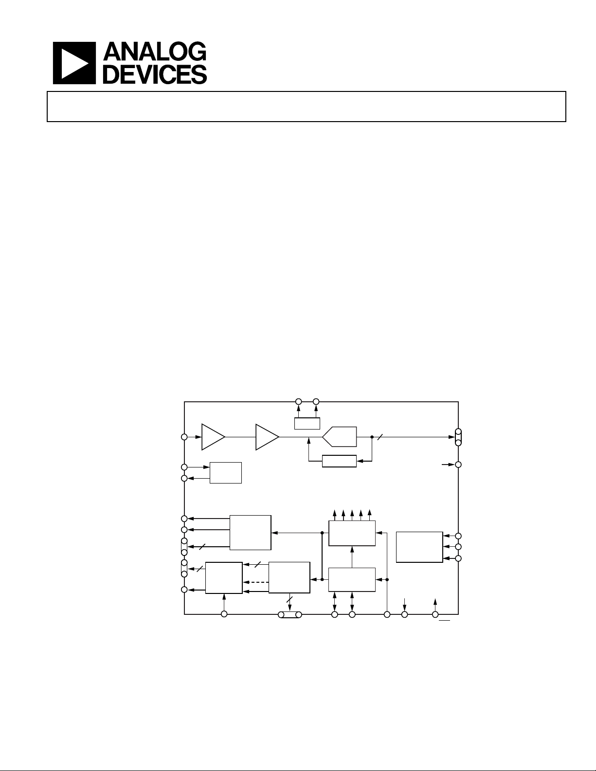
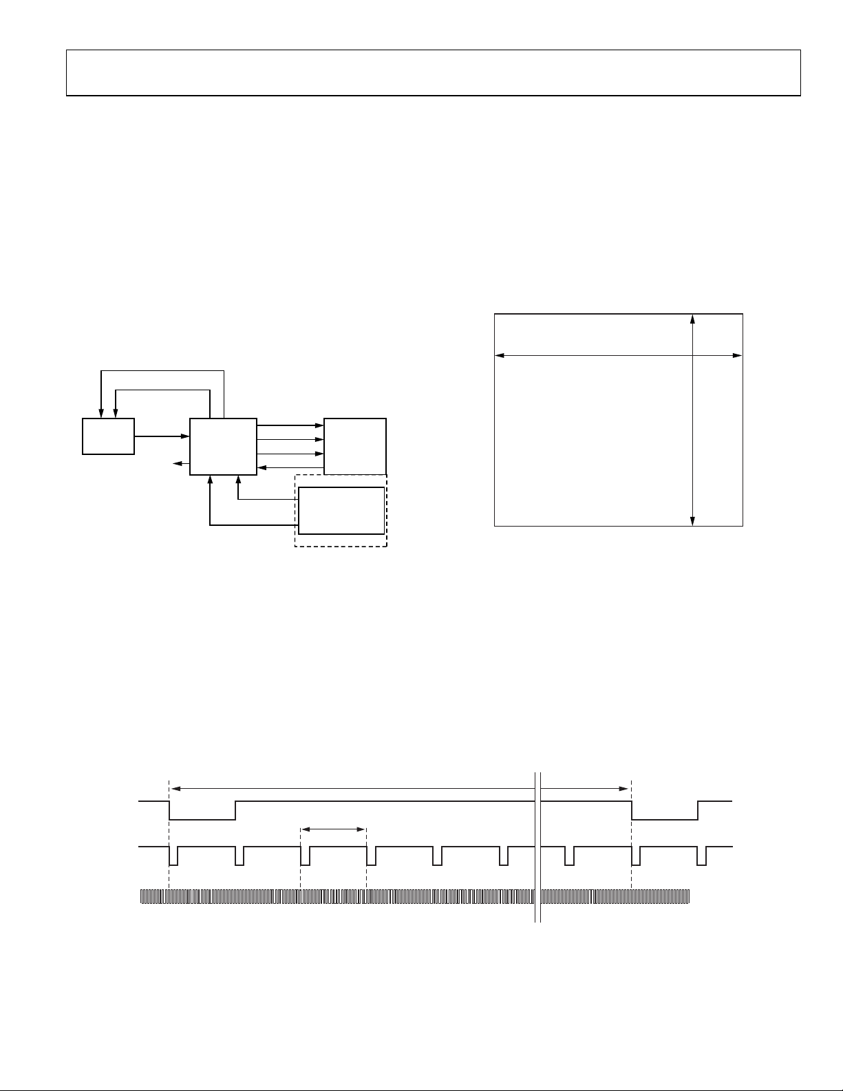
GENERAL DESCRIPTION
The AD9920A is a highly integrated charge-coupled device (CCD)
signal processor for digital still camera applications. It includes a
complete analog front end (AFE) with analog-to-digital conversion,
combined with a full-function programmable timing generator
and 19-channel vertical driver (V-driver). The timing generator
is capable of supporting up to 24 vertical clock signals to control
advanced CCDs. The on-chip V-driver supports up to 19 channels
for use with six-field CCDs. A Precision Timing® core allows adjust-
ment of high speed clocks with approximately 400 ps resolution
at 40.5 MHz operation. The AD9920A also contains six GPOs
that can be used for shutter and system functions.
The analog front end includes black level clamping, variable
gain CDS, and a 12-bit ADC. The timing generator provides all
the necessary CCD clocks: RG, H-clocks, V-clocks, sensor gate
pulses, substrate clock, and substrate bias control.
The AD9920A is specified over an operating temperature range
of −25°C to +85°C.
FUNCTIONAL BLOCK DIAGRAM
REFT REFB
CCDIN
LDOIN
LDOOUT
RG
HL
H1 TO H8
V1A TO V6 (3-LEVEL)
V7 TO V16 (2-LEVEL)
SUBCK
–3dB, 0dB, +3dB, +6dB
CDS
LDO
REG
HORIZONTAL
VERTICAL
DRIVER
XSUBCNT
DRIVERS
XV1 TO XV24
8
19
VGA
6dB TO 42d B
24
GPO5
GPO6
XSUBCK
VREF
VERTICAL
TIMING
CONTROL
6
GPO7, GPO8
12-BIT
ADC
CLAMP
INTERN AL CLOCK S
PRECISION
TIMING
GENERATOR
SYNC
GENERATOR
HD VD
Figure 1.
12
CLI
AD9920A
INTERNAL
REGISTERS
CLOGPO1 TO GPO4,
SYNC/RST
D0 TO D11
DCLK
SL
SCK
SDATA
06878-001
Rev. B
Information furnished by Analog Devices is believed to be accurate and reliable. However, no
responsibility is assumed by Analog Devices for its use, nor for any infringements of patents or other
rights of third parties that may result from its use. Specifications subject to change without notice. No
license is granted by implication or otherwise under any patent or patent rights of Analog Devices.
Trademarks and registered trademarks are the property of their respective owners.
One Technology Way, P.O. Box 9106, Norwood, MA 02062-9106, U.S.A.
Tel: 781.329.4700 www.analog.com
Fax: 781.461.3113 ©2009–2010 Analog Devices, Inc. All rights reserved.

AD9920A
TABLE OF CONTENTS
Features .............................................................................................. 1
Applications ....................................................................................... 1
General Description ......................................................................... 1
Functional Block Diagram .............................................................. 1
Revision History ............................................................................... 3
Specifications ..................................................................................... 4
Digital Specifications ................................................................... 5
Analog Specifications ................................................................... 5
Timing Specifications .................................................................. 7
Vertical Driver Specifications ..................................................... 8
Absolute Maximum Ratings .......................................................... 10
Thermal Resistance .................................................................... 10
ESD Caution ................................................................................ 10
Pin Configuration and Function Descriptions ........................... 11
Typical Performance Characteristics ........................................... 14
Equivalent Circuits ......................................................................... 15
Terminology .................................................................................... 16
Theory of Operation ...................................................................... 17
H-Counter Behavior in Slave Mode ......................................... 17
High Speed Precision Timing Core ........................................... 18
Digital Data Outputs .................................................................. 22
Horizontal Clamping and Blanking ......................................... 23
Horizontal Timing Sequence Example .................................... 30
Vertical Timing Generation ...................................................... 32
Vertical Sequences (VSEQ) ....................................................... 34
Vertical Timing Example ........................................................... 51
Internal Vertical Driver Connections (18-Channel Mode) .. 53
Internal Vertical Driver Connections (19-Channel Mode) .. 54
Output Polarity of Vertical Transfer Clocks and Substrate
Clock ............................................................................................ 55
V-Driver Slew Rate Control ...................................................... 60
Shutter Timing Control ............................................................. 60
Substrate Clock Operation (SUBCK) ...................................... 60
Field Counters ............................................................................. 63
General-Purpose Outputs (GPOs) .......................................... 64
GP Lookup Table (LUT) ............................................................ 68
Complete Exposure/Readout Operation Using Primary
Counter and GPO Signals ......................................................... 69
SG Control Using GPO ............................................................. 71
Manual Shutter Operation Using Enhanced SYNC Modes .. 73
Analog Front End Description and Operation ...................... 77
Applications Information .............................................................. 79
Power-Up Sequence for Master Mode ..................................... 79
Power-Up Sequence for Slave Mode ........................................ 81
Power-Down Sequence for Master and Slave Modes ............ 83
Additional Restrictions in Slave Mode .................................... 84
Vertical Toggle Position Placement Near Counter Reset ...... 85
Standby Mode Operation .......................................................... 86
CLI Frequency Change .............................................................. 86
Circuit Layout Information ........................................................... 88
Typical 3 V System ..................................................................... 88
External Crystal Application .................................................... 88
Circuit Configurations .............................................................. 89
Serial Interface ................................................................................ 93
Serial Interface Timing .............................................................. 93
Layout of Internal Registers ...................................................... 94
Updating New Register Values ................................................. 95
Complete Register Listing ............................................................. 96
Outline Dimensions ..................................................................... 112
Ordering Guide ........................................................................ 112
Rev. B | Page 2 of 112

AD9920A
REVISION HISTORY
6/10—Rev. A to Rev. B
Changes to Figure 1 ........................................................................... 1
Changes to Figure 9, Figure 10, Figure 12, and Figure 13 ......... 15
Moved Terminology Section .......................................................... 16
Changes to Figure 15 ...................................................................... 17
Moved Generating HBLK Line Alternation Section .................. 24
Moved Figure 32 .............................................................................. 25
Moved Figure 33 .............................................................................. 27
Changes to Vertical Sequences (VSEQ) Section ......................... 34
Changes to Special Vertical Sequence Alternation
(SVSA) Mode Section ..................................................................... 38
Added Table 18; Renumbered Tables Sequentially ..................... 44
Deleted Figure 77; Renumbered Figures Sequentially ............... 61
Changes to SUBCK Low Speed Operation Section
and Table 43 ..................................................................................... 61
Changes to Figure 81 ...................................................................... 62
Changes to Table 45 ........................................................................ 64
Changes to Scheduled Toggles Section and Figure 85 ............... 66
Changes to Figure 86, ShotTimer Sequences Section,
and Figure 87 ................................................................................... 67
Changes to Complete Exposure/Readout Operation
Using Primary Counter and GPO Signals Section ..................... 69
Changes to Triggered Control of GPO5 Section ......................... 71
Changes to Figure 96 ...................................................................... 75
Changes to Figure 100 .................................................................... 77
Changes to Figure 102 .................................................................... 80
Changes to Power-Up Sequence for Slave Mode Section .......... 81
Changes to Figure 103 .................................................................... 82
Changes to Power-Down Sequence for Master and
Slave Modes Section........................................................................ 83
Added Table 48; Renumbered Tables Sequentially ..................... 86
Changes to Figure 108 .................................................................... 88
Changes to Figure 109 .................................................................... 89
Changes to Figure 110 .................................................................... 90
Changes to Figure 111 .................................................................... 91
Changes to Figure 112 .................................................................... 92
Changes to Layout of Internal Registers Section
and Figure 115 ................................................................................. 94
Changes to Table 53 ........................................................................ 97
Changes to Table 57 ........................................................................ 99
Changes to Table 59 ...................................................................... 101
Changes to Table 61 ...................................................................... 105
Changes to Table 63 ...................................................................... 108
Updated Outline Dimensions ...................................................... 112
6/09—Revision A: Initial Version
Rev. B | Page 3 of 112

AD9920A
SPECIFICATIONS
Table 1.
Parameter Test Conditions/Comments Min Typ Max Unit
TEMPERATURE RANGE
Operating −25 +85 °C
Storage −65 +150 °C
POWER SUPPLY VOLTAGE INPUTS
AVDD AFE analog supply 1.6 1.8 2.0 V
TCVDD Timing core supply 1.6 1.8 2.0 V
CLIVDD CLI input supply 1.6 3.0 3.6 V
RGVDD RG, HL driver supply 2.1 3.0 3.6 V
HVDD1 and HVDD2 H1 to H8 driver supplies 2.1 3.0 3.6 V
DVDD Digital logic supply 1.6 1.8 2.0 V
DRVDD Parallel data output driver supply 1.6 3.0 3.6 V
IOVDD Digital I/O supply 1.6 3.0 3.6 V
V-DRIVER POWER SUPPLY VOLTAGES
VDVDD V-driver/logic supply 1.6 3.0 3.6 V
VH1, VH2 V-driver high supply 11.0 15.0 16.5 V
VL1, VL2 V-driver low supply −8.5 −7.5 −5.5 V
VM1, VM2 V-driver midsupply −1.5 0.0 +1.5 V
VLL SUBCK low supply −11.0 −7.5 −5.5 V
VH1, VH2 to VL1, VL2, VLL 23.5 V
1
VMM
2
LDO
LDOIN LDO supply input 2.5 3.0 3.6 V
Output Voltage 1.8 1.9 2.05 V
Output Current 60 100 mA
POWER SUPPLY CURRENTS—40.5 MHz
OPERATION
AVDD 1.8 V 27 mA
TCVDD 1.8 V 5 mA
CLIVDD 3 V 1.5 mA
RGVDD 3.3 V, 20 pF RG load, 20 pF HL load 10 mA
HVDD1 and HVDD2
3
DVDD 1.8 V 9.5 mA
DRVDD
IOVDD
POWER SUPPLY CURRENTS—STANDBY
MODE OPERATION
Standby1 Mode 20 mA
Standby2 Mode 5 mA
Standby3 Mode 1.5 mA
MAXIMUM CLOCK RATE (CLI) 40.5 MHz
MINIMUM CLOCK RATE (CLI) 10 MHz
1
VMM must be greater than VLL and less than VDVDD.
2
LDO should be used only for the AD9920A 1.8 V supplies, not for external circuitry.
3
The total power dissipated by the HVDD (or RGVDD) can be approximated using the following equation:
Total HVDD Power = (CL × HVDD × Pixel Frequency) × HVDD
SUBCK midsupply VLL 0.0 VDVDD V
3.3 V, 480 pF total load on H1 to H8 59 mA
3 V, 10 pF load on each data output pin
6 mA
(D0 to D11)
3 V, depends on load and output
2 mA
frequency of digital I/O
Rev. B | Page 4 of 112
AD9920A
DIGITAL SPECIFICATIONS
IOVDD = 1.6 V to 3.6 V, RGVDD = HVDD1 and HVDD2 = 2.7 V to 3.6 V, CL = 20 pF, T
Table 2.
Parameter Symbol Test Conditions/Comments Min Typ Max Unit
LOGIC INPUTS (IOVDD)
High Level Input Voltage VIH V
Low Level Input Voltage VIL 0.6 V
High Level Input Current IIH 10 μA
Low Level Input Current IIL 10 μA
Input Capacitance CIN 10 pF
LOGIC OUTPUTS (IOVDD, DRVDD)
High Level Output Voltage VOH I
Low Level Output Voltage VOL I
RG and H-DRIVER OUTPUTS (HVDD1,
= 2 mA VDD − 0.5 V
OH
= 2 mA 0.5 V
OL
HVDD2, and RGVDD)
High Level Output Voltage VOH Maximum current VDD − 0.5 V
Low Level Output Voltage VOL Maximum current 0.5 V
Maximum H1 to H8 Output Current Programmable 30 mA
Maximum HL and RG Output Current Programmable 17 mA
Maximum Load Capacitance Each output 60 pF
CLI INPUT With CLO oscillator disabled
High Level Input Voltage V
Low Level Input Voltage V
CLIVDD/2 + 0.5 V
IHCLI
CLIVDD/2 − 0.5 V
ILCLI
to T
MIN
− 0.6 V
DD
, unless otherwise noted.
MAX
ANALOG SPECIFICATIONS
AVDD = 1.8 V, f
Table 3.
Parameter Test Conditions/Comments Min Typ Max Unit
1
CDS
DC Restore AVDD − 0.5 V 1.21 1.3 1.44 V
Allowable CCD Reset Transient Limit is the lower of AVDD + 0.3 V or 2.2 V 0.5 0.8 V
CDS Gain Accuracy VGA gain = 6.3 dB (Code 15, default value)
−3 dB CDS Gain −3.1 −2.6 −2.1 dB
0 dB CDS Gain −0.6 −0.1 +0.4 dB
+3 dB CDS Gain 2.7 3.2 3.7 dB
+6 dB CDS Gain 5.2 5.7 6.2 dB
Maximum Input Range Before
Saturation
−3 dB CDS Gain 1.4 V p-p
0 dB CDS Gain 1.0 V p-p
+3 dB CDS Gain 0.7 V p-p
+6 dB CDS Gain 0.5 V p-p
Allowable OB Pixel Amplitude
0 dB CDS Gain (Default) −100 +200 mV
+6 dB CDS Gain −50 +100 mV
VARIABLE GAIN AMPLIFIER (VGA)
Gain Control Resolution 1024 Steps
Gain Monotonicity Guaranteed
Gain Range
Low Gain VGA Code 15, default 6.3 dB
Maximum Gain VGA Code 1023 42.4 dB
= 40.5 MHz, typical timing specifications, T
CLI
1
MIN
to T
, unless otherwise noted.
MAX
Rev. B | Page 5 of 112
AD9920A
Parameter Test Conditions/Comments Min Typ Max Unit
BLACK LEVEL CLAMP
Clamp Level Resolution 1024 Steps
Clamp Level Measured at ADC output
Minimum Clamp Level Code 0 0 LSB
Maximum Clamp Level Code 1023 255 LSB
ADC
Resolution 12 Bits
Differential Nonlinearity (DNL)
No Missing Codes Guaranteed
Integral Nonlinearity (INL)
Full-Scale Input Voltage 2.0 V
VOLTAGE REFERENCE
Reference Top Voltage (REFT) 1.4 V
Reference Bottom Voltage (REFB) 0.4 V
SYSTEM PERFORMANCE Includes entire signal chain
Gain Accuracy 0 dB CDS gain
Low Gain
Maximum Gain VGA Code 1023 41.8 42.3 42.8 dB
Peak Nonlinearity, 1 V Input Signal
Total Output Noise
2
Power Supply Rejection (PSR)
1
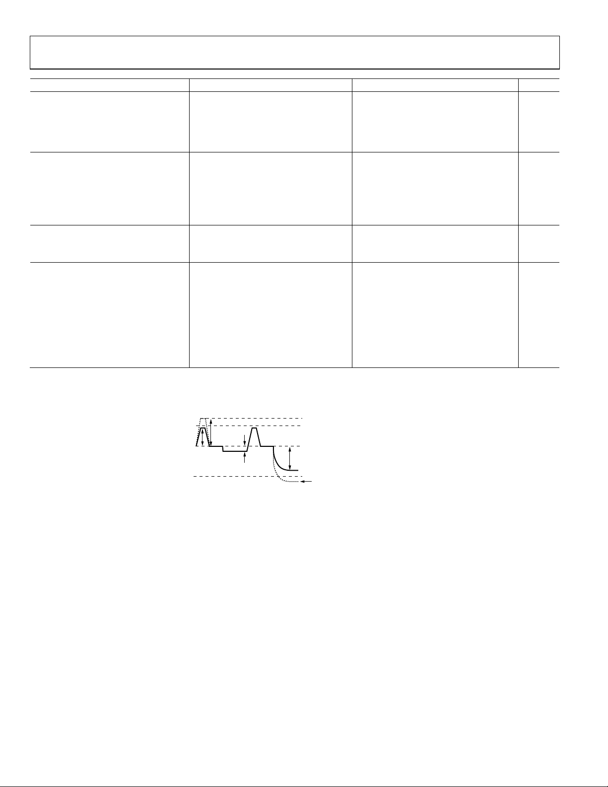
Input signal characteristics are defined as shown in Figure 2.
2
See the Terminology section.
2
2
±3.0 LSB
±0.5 LSB
VGA Code 15
5.7 6.2 6.7 dB
Gain = (0.0358 × code) + 5.76 dB
2
6 dB VGA gain, 0 dB CDS gain applied 0.1 0.3 %
AC-grounded input, 6 dB VGA gain
0.6 LSB rms
applied
2
Measured with step change on supply 40 dB
MAXIMUM INPUT LIMIT = L E SSE R OF
2.2V OR AVDD + 0.3V
800mV
MAXIMUM
500mV TYP
RESET TRANSIENT
200mV MAX
OPTICAL BL ACK PI X EL
Figure 2. Input Signal Characteristics
+1.8V TYP (AVDD)
+1.3V TYP (AVDD – 0.5V)
DC RESTORE VOLTAGE
1V MAXIMUM INPUT SIGNAL RANGE
(0dB CDS GAIN)
0V (AVSS)
MINIMUM INPUT LIMIT
(AVSS – 0.3V )
06878-002
Rev. B | Page 6 of 112
AD9920A
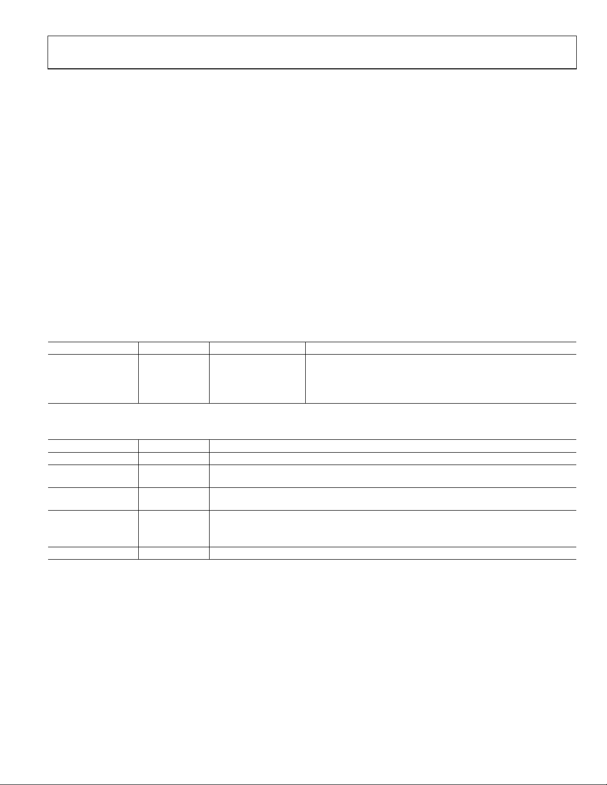
TIMING SPECIFICATIONS
CL = 20 pF, AVDD = DVDD = TCVDD = 1.8 V, f
Table 4.
Parameter
MASTER CLOCK See Figure 18
CLI Clock Period t
CLI High/Low Pulse Width 0.8 × t
Delay from CLI Rising Edge to Internal
Pixel Position 0
SLAVE MODE SPECIFICATIONS See Figure 105
VD Falling Edge to HD Falling Edge t
HD Falling Edge to CLI Rising Edge
HD Falling Edge to CLO Rising Edge
CLI Rising Edge to SHPLOC Internal sample edge t
AFE
SHPLOC Sample Edge to SHDLOC
Sample Edge
SHDLOC Sample Edge to SHPLOC
Sample Edge
AFE Pipeline Delay See Figure 26 16 Cycles
AFE CLPOB Pulse Width 2 20 Pixels
DATA OUTPUTS
Output Delay from DCLK Rising Edge See Figure 25 tOD 1 ns
Pipeline Delay from SHP/SHD
Sampling to Data Output
SERIAL INTERFACE
Maximum SCK Frequency
SL to SCK Setup Time tLS 10 ns
SCK to SL Hold Time tLH 10 ns
SDATA Valid to SCK Rising Edge Setup tDS 10 ns
SCK Falling Edge to SDATA Valid Hold tDH 10 ns
TIMING CORE SETTING RESTRICTIONS
Inhibited Region for SHP Edge
Location
Inhibited Region for SHP or SHD with
Respect to H-Clocks
1
2, 3, 4
RETIME = 0, MASK = 0 t
RETIME = 0, MASK = 1 t
RETIME = 1, MASK = 0 t
RETIME = 1, MASK = 1 t
Inhibited Region for DOUTPHASE Edge
Location
1
Applies only to slave mode operation. The inhibited area for SHP is needed to meet the timing requirement for t
2
When the HBLKRETIME bits (Address 0x35, Bits[3:0]) are enabled, the inhibit region for the SHD location changes to the inhibit region for the SHP location.
3
When the HBLK masking polarity registers (V-sequence Register 0x18[24:21]) are set to 0, the H-edge reference becomes HxNEGLOC.
4
The H-clock signals that have SHP/SHD inhibit regions depend on the HCLK mode: Mode 1 = H1; Mode 2 = H1, H2; Mode 3 = H1, H3; and 3-Phase Mode = Phase 1,
Phase 2, and Phase 3.
= 40.5 MHz, unless otherwise noted.
CLI
Test Conditions/
Comments Symbol Min Typ Max Unit
24.7 ns
CONV
/2 t
CONV
t
Only valid if OSC_RST
Only valid if OSC_RST
See Figure 23
See Figure 23
= 0
= 1
t
t
6 ns
CLIDLY
0 VD period − t
VDHD
t
3 t
HDCLI
t
3 t
HDCLO
3 t
CLISHP
0.8 × t
S1
0.8 × t
S2
CONV
CONV
/2 t
/2 t
/2 1.2 × t
CONV
/2 t
CONV
/2 t
CONV
/2 ns
CONV
ns
CONV
− 2 ns
CONV
− 2 ns
CONV
− 2 ns
CONV
− tS2 ns
CONV
− tS1 ns
CONV
16 Cycles
40.5 MHz
Must not exceed CLI
f
SCLK
frequency
See Figure 23 t
50 62
SHPINH
Edge
location
See Figure 23 and
Figure 24
HxNEGLOC − 14 HxNEGLOC − 2
SHDINH
Edge
location
HxPOSLOC − 14 HxPOSLOC − 2
SHDINH
Edge
location
HxNEGLOC − 14 HxNEGLOC − 2
SHPINH
Edge
location
HxPOSLOC − 14 HxPOSLOC − 2
SHPINH
Edge
location
See Figure 23
t
SHDLOC + 1 SHDLOC + 12
DOUTINH
Edge
location
for proper H-counter reset operation.
CLISHP
Rev. B | Page 7 of 112
AD9920A
VERTICAL DRIVER SPECIFICATIONS
VH1, VH2 = 12 V; VM1, VM2, VMM = 0 V; VL1, VL2, VLL = −6 V; CL shown in load model; TA = 25°C.
Table 5.
Parameter Symbol Test Conditions/Comments Min Typ Max Unit
V1A TO V13
Simplified load conditions, 3000 pF to
ground + 30 Ω in series, SRSW = VSS
Delay Time, VL to VM and VM to VH t
Delay Time, VM to VL and VH to VM t
Rise Time, VL to VM t
Rise Time, VM to VH t
Fall Time, VM to VL t
Fall Time, VH to VM t
, t
40 ns
PLM
PMH
, t
40 ns
PML
PHM
150 ns
RLM
315 ns
RMH
250 ns
FML
165 ns
FHM
Output Currents
At −7.25 V 10 mA
At −0.25 V −22 mA
At +0.25 V 22 mA
At +14.75 V −10 mA
RON 35 Ω
V14, V15, V16
Simplified load conditions, 3000 pF to
ground + 30 Ω in series
Delay Time, VL to VM t
Delay Time, VM to VL t
Rise Time, VL to VM t
Fall Time, VM to VL t
45 ns
PLM
45 ns
PML
345 ns
RLM
280 ns
FML
Output Currents
At −7.25 V 10 mA
At −0.25 V −7 mA
RON 55 Ω
SUBCK OUTPUT Simplified load conditions, 1000 pF to ground
Delay Time, VLL to VH t
Delay Time, VH to VLL t
Delay Time, VLL to VMM t
Delay Time, VMM to VH t
Delay Time, VH to VMM t
Delay Time, VMM to VLL t
Rise Time, VLL to VH t
Rise Time, VLL to VMM t
Rise Time, VMM to VH t
Fall Time, VH to VLL t
Fall Time, VH to VMM t
Fall Time, VMM to VLL t
50 ns
PLH
50 ns
PHL
50 ns
PLM
50 ns
PMH
50 ns
PHM
50 ns
PML
50 ns
RLH
55 ns
RLM
50 ns
RMH
55 ns
FHL
100 ns
FHM
40 ns
FML
Output Currents
At −7.25 V 20 mA
At −0.25 V −12 mA
At +0.25 V 12 mA
At +14.75 V −20 mA
RON 35 Ω
SRCTL INPUT RANGE Valid only when SRSW is high 0.8 VDVDD V
Rev. B | Page 8 of 112
AD9920A
V-DRIVER
INPUT
V-DRIVER
OUTPUT
50%
10%
90%
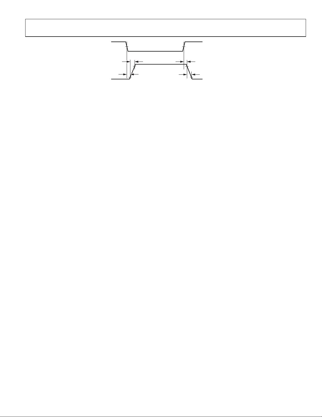
t
PLM
t
,
t
,
RLM
t
RMH
RLH
,
t
,
t
PMH
PLH
50%
90%
10%
t
PML
t
,
FML
t
Figure 3. Definition of V-Driver Timing Specifications
PHM
,
t
FHM
,
t
PHL
,
t
FHL
06878-003
Rev. B | Page 9 of 112
AD9920A
ABSOLUTE MAXIMUM RATINGS
Table 6.
Parameter Rating
AVDD to AVSS −0.3 V to +2.2 V
TCVDD to TCVSS −0.3 V to +2.2 V
HVDD1, HVDD2 to HVSS1, HVSS2 −0.3 V to +3.9 V
RGVDD to RGVSS −0.3 V to +3.9 V
DVDD to DVSS −0.3 V to +2.2 V
DRVDD to DRVSS/LDOVSS −0.3 V to +3.9 V
IOVDD to IOVSS −0.3 V to +3.9 V
VDVDD to VDVSS −0.3 V to +3.9 V
CLIVDD to TCVSS −0.3 V to +3.9 V
VH1, VH2 to VL1, VL2, VLL −0.3 V to +25.0 V
VH1, VH2 to VDVSS −0.3 V to +17.0 V
VL1, VL2 to VDVSS −17.0 V to +0.3 V
VM1, VM2 to VDVSS −6.0 V to +3.0 V
VLL to VDVSS −17.0 V to +0.3 V
VMM to VDVSS VLL − 0.3 V to VDVDD + 0.3 V
V1A to V16 to VDVSS VLx − 0.3 V to VHx + 0.3 V
RG and HL Outputs to RGVSS −0.3 V to RGVDD + 0.3 V
H1 to H8 Outputs to HVSSx −0.3 V to HVDDx + 0.3 V
VDR_EN, XSUBCNT, SRCTL, SRSW
to VDVSS
Digital Outputs to IOVSS −0.3 V to IOVDD + 0.3 V
Digital Inputs to IOVSS −0.3 V to IOVDD + 0.3 V
SCK, SL, SDATA to DVSS −0.3 V to DVDD + 0.3 V
REFT, REFB, CCDIN to AVSS −0.3 V to AVDD + 0.3 V
Junction Temperature 150°C
Lead Temperature
(Soldering, 10 sec)
−0.3 V to VDVDD + 0.3 V
350°C
Stresses above those listed under Absolute Maximum Ratings
may cause permanent damage to the device. This is a stress
rating only; functional operation of the device at these or any
other conditions above those indicated in the operational
section of this specification is not implied. Exposure to absolute
maximum rating conditions for extended periods may affect
device reliability.
THERMAL RESISTANCE
θJA is specified for the worst-case conditions, that is, a device
soldered in a circuit board for surface-mount packages.
Table 7. Thermal Resistance
Package Type θJA Unit
CSP_BGA (BC-105-1) 40.3 °C/W
ESD CAUTION
Rev. B | Page 10 of 112
AD9920A
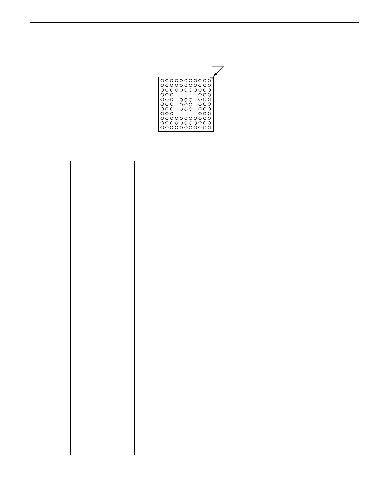
A
PIN CONFIGURATION AND FUNCTION DESCRIPTIONS
1 CORNER
1110987654321
Figure 4. Pin Configuration
Table 8. Pin Function Descriptions
Pin No. Mnemonic Type1Description
L6 AVDD P Analog Supply.
J7, K8 AVSS P Analog Supply Ground.
A10 DVDD P Digital Logic Supply.
A9 DVSS P Digital Logic Ground.
L5 CLIVDD P CLI Input Supply.
K6 TCVDD P Analog Timing Core Supply.
K4 TCVSS P Analog Timing Core Ground.
A2 DRVDD P Data Driver Supply.
B2 DRVSS/LDOVSS P Data Driver and LDO Ground.
E1 HVDD1 P H-Driver Supply.
E2 HVSS1 P H-Driver Ground.
G1 HVDD2 P H-Driver Supply.
G2 HVSS2 P H-Driver Ground.
J1 HVDD2 P H-Driver Supply.
J2 HVSS2 P H-Driver Ground.
L3 RGVDD P RG, HL Driver Supply.
K3 RGVSS P RG, HL Driver Ground.
B1 LDOIN P LDO 3.3 V Input.
C1 LDOOUT P LDO Output Voltage.
H11 IOVDD P Digital I/O Supply.
G11 IOVSS P Digital I/O Ground.
C11 VDVDD P V-Driver Logic Supply (3 V).
C10 VDVSS P V-Driver Ground.
E3 VM1 P V-Driver Midsupply.
D3 VL1 P V-Driver Low Supply.
C3 VH1 P V-Driver High Supply.
J3 VH2 P V-Driver High Supply.
H3 VL2 P V-Driver Low Supply.
F3 VM2 P V-Driver Midsupply.
G3 VMM P V-Driver Midsupply for SUBCK Output.
J4 VLL P V-Driver Low Supply for SUBCK Output.
L7 CCDIN AI CCD Signal Input.
K7 CCDGND AI CCD Ground.
C2 SRCTL AI Slew Rate Control Pin. Tie to VDVSS if not used.
L8 REFT AO Voltage Reference Top Bypass.
L9 REFB AO Voltage Reference Bottom Bypass.
D11 VD DIO Vertical Sync Pulse.
E10 HD DIO Horizontal Sync Pulse.
INDEX AREA
BOTTOM V I EW
(Not to S cale)
A
B
C
D
E
F
G
H
J
K
L
06878-004
Rev. B | Page 11 of 112
AD9920A
Pin No. Mnemonic Type1Description
E11
SYNC/RST
K9 SL DI 3-Wire Serial Load Pulse (Internal Pull-Up Resistor).
K10 SDATA DI 3-Wire Serial Data.
L10 SCK DI 3-Wire Serial Clock.
B11 VDR_EN DI Enable V-Outputs When High.
K11 XSUBCNT DI XSUBCNT Input to SUBCK Buffer.
C9 SRSW DI Slew Rate Control Enable. Tie to ground to disable.
J6
LEGEN
J5 CLI DI Reference Clock Input.
K5 CLO DO Clock Output for Crystal.
F10 GPO1 DO General-Purpose Output.
H9 GPO2 DO General-Purpose Output.
G10 GPO3 DO General-Purpose Output.
F11 GPO4 DO General-Purpose Output.
H10 GPO7 DO General-Purpose Output.
J11 GPO8 DO General-Purpose Output.
B9 D0 DO Data Output (LSB).
C6 D1 DO Data Output.
C7 D2 DO Data Output.
A8 D3 DO Data Output.
A7 D4 DO Data Output.
B7 D5 DO Data Output.
B6 D6 DO Data Output.
A6 D7 DO Data Output.
A5 D8 DO Data Output.
B4 D9 DO Data Output.
A4 D10 DO Data Output.
A3 D11 DO Data Output (MSB).
B3 DCLK DO Data Clock Output.
D1 H1 DO CCD Horizontal Clock.
D2 H2 DO CCD Horizontal Clock.
F1 H3 DO CCD Horizontal Clock.
F2 H4 DO CCD Horizontal Clock.
H1 H5 DO CCD Horizontal Clock.
H2 H6 DO CCD Horizontal Clock.
K1 H7 DO CCD Horizontal Clock.
K2 H8 DO CCD Horizontal Clock.
L2 HL DO CCD Horizontal Clock.
L4 RG DO CCD Reset Gate Clock.
G9 V1A VO3 CCD Vertical Transfer Clock. Three-level output (XV1 + XV16).
G6 V1B VO3 CCD Vertical Transfer Clock. Three-level output (XV1 + XV17).
G5 V2A VO3 CCD Vertical Transfer Clock. Three-level output (XV2 + XV18).
E9 V2B VO3 CCD Vertical Transfer Clock. Three-level output (XV2 + XV19).
J9 V3A VO3 CCD Vertical Transfer Clock. Three-level output (XV3 + XV20).
F6 V3B VO3
F5 V4 VO3 CCD Vertical Transfer Clock. Three-level output (XV4 + XV22).
E5 V5 VO3
D10 V6 VO3
F9 V7 VO2 CCD Vertical Transfer Clock. Two-level output (XV7).
F7 V8 VO2 CCD Vertical Transfer Clock. Two-level output (XV8).
DO SYNC Pin (Internal Pull-Up Resistor)/External Reset Input (Active Low).
DI Legacy Mode Enable Bar. Tie to ground for legacy 18-channel mode.
CCD Vertical Transfer Clock. Three-level output. LEGEN
is low, XV3 + XV21. LEGEN is high,
XV23 + XV21.
CCD Vertical Transfer Clock. Three-level output. LEGEN
is low, XV5 + XV23. LEGEN is high,
XV5 + GPO5.
CCD Vertical Transfer Clock. Three-level output. LEGEN
is low, XV6 + XV24. LEGEN is high,
XV6 + GPO6.
Rev. B | Page 12 of 112
AD9920A
Pin No. Mnemonic Type1Description
D9 V9 VO2 CCD Vertical Transfer Clock. Two-level output (XV9).
C4 V10 VO2 CCD Vertical Transfer Clock. Two-level output (XV10).
C5 V11 VO2 CCD Vertical Transfer Clock. Two-level output (XV11).
B5 V12 VO2 CCD Vertical Transfer Clock. Two-level output (XV12).
E6 V13 VO2 CCD Vertical Transfer Clock. Two-level output (XV13).
E7 V14 VO2 CCD Vertical Transfer Clock. Two-level output (XV14).
C8 V15 VO2 CCD Vertical Transfer Clock. Two-level output (XV15).
J8 V16 VO2
CCD Vertical Transfer Clock. Two-level output (XV24). Available only when LEGEN
(19-channel mode).
G7 SUBCK VO3 CCD Substrate Clock Output.
A1, A11, B8,
NC Not Internally Connected.
B10, J10, L1,
L11
1
AI = analog input; AO = analog output; DI = digital input; DO = digital output; DIO = digital input/output; P = power; VO2 = vertical driver output, two-level;
VO3 = vertical driver output, three-level.
is high
Rev. B | Page 13 of 112
AD9920A
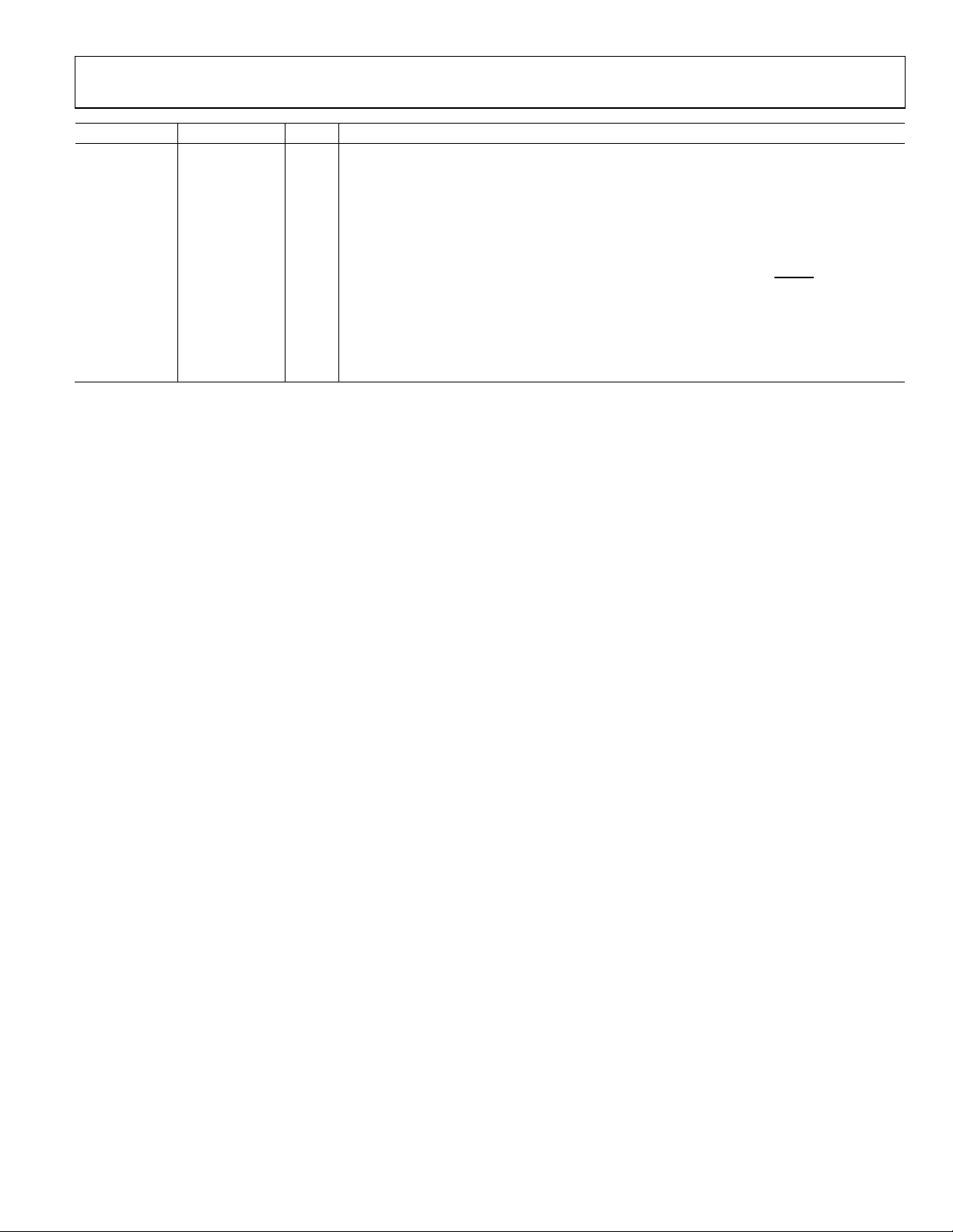
TYPICAL PERFORMANCE CHARACTERISTICS
400
350
3.3V, 2.0V
3.0
2.5
300
250
200
150
POWER (mW)
100
50
0
18 32 40
FREQUENCY (MHz )
3.0V, 1.8V
2.7V, 1.6V
Figure 5. AFETG Power vs. Frequency (V-Driver Not Included);
AVDD = TCVDD = DVDD = 1.8 V, All Other Supplies at 2.7 V, 3.0 V, or 3.3 V
1.0
0.8
0.6
0.4
0.2
0
DNL (LSB)
–0.2
–0.4
–0.6
–0.8
–1.0
0 0.5k 1.0k 1.5k 2.0k 2.5k 3.0k 3.5k 4.0k
ADC OUTPUT CODE
Figure 6. Typical Differential Nonlinearity (DNL) Performance
2.0
1.5
1.0
INL (LSB)
0.5
0
–0.5
06878-005
–1.0
0
0.5k 1.0k 1.5k 2.0k 2.5k 3.0k 3.5k 4.0k
ADC OUTPUT CODE
06878-007
Figure 7. Typical System Integral Nonlinearity (INL) Performance
50
45
40
35
30
25
20
15
RMS OUTPUT NOISE (LS B)
10
5
0
06878-006
0 10203040506
–3dB CD S GA IN
0dB CDS GAIN
+3dB CDS GAIN
+6dB CDS GAIN
TOTAL GAIN — CDS + VGA (dB)
06878-008
0
Figure 8. Output Noise vs. Total Gain (CDS + VGA)
Rev. B | Page 14 of 112
AD9920A
A
V
T
V
V
V
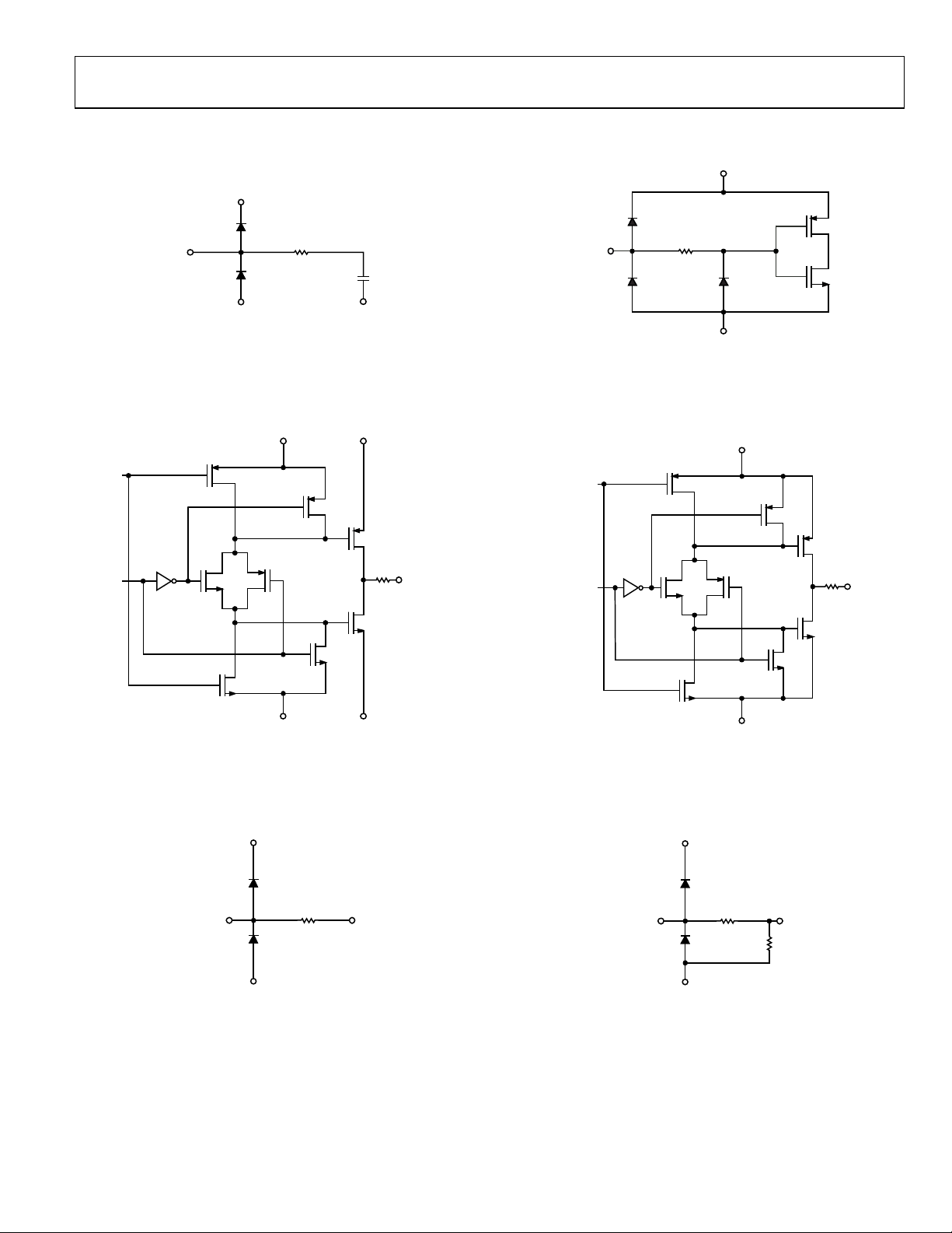
EQUIVALENT CIRCUITS
IOVDD
DD
DATA
HREESTATE
CCDIN
R
AVSS AVSS
Figure 9. CCDIN
DVDD
DRVDD
06878-009
D0 TO D11
DIGITAL
INPUTS
RG, HL, H1 TO H8
THREE-STATE
330Ω
IOVSS
Figure 12. Digital Inputs
HVDD OR
RGVDD
06878-012
OUTPUT
DVSS DRVSS
Figure 10. Digital Data Outputs
DVDD
XSUBCNT
VDVSS
Figure 11. XSUBCNT
3.5k
Ω
06878-011
06878-010
HVSS OR
RGVSS
06878-013
Figure 13. H1 to H8, HL, RG Drivers
DVDD
Ω
VDVSS
3.5k
R
06878-014
DR_EN
Figure 14. VDR_EN
Rev. B | Page 15 of 112

AD9920A
TERMINOLOGY
Differential Nonlinearity (DNL)
An ideal ADC exhibits code transitions that are exactly 1 LSB
apart. DNL is the deviation from this ideal value. It is often
specified in terms of resolution for which no missing codes are
guaranteed. No missing codes guaranteed to 12-bit resolution
indicates that all 4096 codes, each for its respective input, must
be present over all operating conditions.
Integral Nonlinearity (INL)
INL is defined as the maximum deviation of the actual analog
output from the ideal output, determined by a straight line
drawn from zero scale to full scale.
Peak Nonlinearity
Peak nonlinearity, a full signal chain specification, refers to the
peak deviation of the output of the AD9920A from a true straight
line. The point used as zero scale occurs 0.5 LSB before the first
code transition. Positive full scale is defined as a level 1 LSB and
0.5 LSB beyond the last code transition. The deviation is measured
from the middle of each particular output code to the true straight
line. The error is then expressed as a percentage of the 2 V ADC
full-scale signal. The input signal is always appropriately amplified
to fill the ADC full-scale range.
Power Supply Rejection (PSR)
The PSR is measured with a step change applied to the supply
pins. The PSR specification is calculated from the change in the
data outputs for a given step change in the supply voltage.
Tot a l O ut p ut Noi se
The rms output noise is measured using histogram techniques.
The standard deviation of the ADC output codes is calculated
in LSB and represents the rms noise level of the total signal
chain at the specified gain setting. The output noise can be
converted to an equivalent voltage using the relationship
1 LSB = (ADC Full Scale/2
where n is the bit resolution of the ADC.
For the AD9920A, 1 LSB = 0.244 mV.
n
Codes)
Rev. B | Page 16 of 112
AD9920A
V
THEORY OF OPERATION
Figure 15 shows the typical system block diagram for the AD9920A
in master mode. The CCD output is processed by the AD9920A
AFE circuitry, which consists of a CDS, black level clamp, and
ADC. The digitized pixel information is sent to the digital image
processor chip, which performs the postprocessing and compression. To operate the CCD, all CCD timing parameters are
programmed into the AD9920A from the system microprocessor
through the 3-wire serial interface. From the master clock, CLI,
provided by the image processor or external crystal, the AD9920A
generates the CCD horizontal and vertical clocks and the internal
AFE clocks. External synchronization is provided by a sync pulse
from the microprocessor, which resets the internal counters and
resyncs the VD and HD outputs.
1A TO V16, SUBCK
H1 TO H8, HL ,
RG, VSUB
CCD
GPO1 TO GPO8
CCDIN
Figure 15. Typical System Block Diagram, Master Mode
AD9920A
V-DRIVER
SYNC
AFETG
D0 TO D11
DCLK
HD, VD
SERIAL
INTERFACE
CLI
MICROPROCESSOR
DIGITAL
IMAGE
PROCESSING
ASIC
Alternatively, the AD9920A can be operated in slave mode. In
this mode, the VD and HD are provided externally from the
image processor, and all AD9920A timing is synchronized with
VD and HD.
The H-drivers for H1 to H8, HL, and RG are included in the
AD9920A, allowing these clocks to be directly connected to the
CCD. An H-driver voltage of up to 3.6 V is supported. V1A to
V16 and SUBCK vertical clocks are included as well, allowing
the AD9920A to provide all horizontal and vertical clocks
necessary to clock data out of a CCD.
MAXIMUM VD LENGTH I S 8192 LINES
06878-015
The AD9920A includes programmable general-purpose outputs
(GPOs) that can trigger mechanical shutter and strobe (flash)
circuitry.
Figure 16 and Figure 17 show the maximum horizontal and
vertical counter dimensions for the AD9920A. All internal
horizontal and vertical clocking is controlled by these counters,
which specify line and pixel locations. Maximum HD length is
16,384 pixels per line, and maximum VD length is 8192 lines
per field.
MAXIMUM COUNT E R DIMENSIONS
14-BIT HORIZONTAL = 16,384 PIXE LS MAXIMUM
13-BIT VERTICAL = 8192 LINES MAXIMUM
06878-016
Figure 16. Vertical and Horizontal Counters
H-COUNTER BEHAVIOR IN SLAVE MODE
In the AD9920A, the internal H-counter holds at its maximum
count of 16,383 instead of rolling over. This feature allows the
AD9920A to be used in applications that contain a line length
greater than 16,384 pixels. Although no programming values
for the vertical and horizontal signals are available beyond 8191,
the H, RG, and AFE clocking continues to operate, sampling the
remaining pixels on the line.
VD
HD
CLI
MAXIMUM HD LENGTH IS 16,384 PIXELS
Figure 17. Maximum VD/HD Dimensions
06878-017
Rev. B | Page 17 of 112
AD9920A
HIGH SPEED PRECISION TIMING CORE
The AD9920A generates high speed timing signals using the
flexible Precision Timing core. This core is the foundation for
generating the timing used for both the CCD and the AFE; it
includes the reset gate (RG), horizontal drivers (H1 to H8, HL),
and SHP/SHD sample clocks. A unique architecture makes it
routine for the system designer to optimize image quality by
providing precise control over the horizontal CCD readout
and the AFE correlated double sampling.
The high speed timing of the AD9920A operates the same
way in either master or slave mode configuration. For more
information on synchronization and pipeline delays, see
the Power-Up Sequence for Master Mode section.
Timing Resolution
The Precision Timing core uses a 1× master clock input as a
reference (CLI). This clock should be the same as the CCD pixel
clock frequency. Figure 18 illustrates how the internal timing core
POSITION
CLI
t
CLIDLY
1 PIXEL
PERIOD
NOTES
1. PIXEL CLOCK PERIOD IS DIVIDED INTO 64 POSITIONS, PROVIDING FINE EDGE RESOLUTION FOR HIGH SPEED CLOCKS.
2. THERE IS A FIXED DELAY FROM THE CLI INPUTTO THE INTERNAL PIXEL PERIOD POSITIONS (
P[0] P[64] = P[0]P[16] P[32] P[48]
...
Figure 18. High Speed Clock Resolution from CLI, Master Clock Input
1
divides the master clock period into 64 steps or edge positions.
Using a 40.5 MHz CLI frequency, the edge resolution of the
Precision Timing core is approximately 0.4 ns. If a 1× system clock
is not available, it is possible to use a 2× reference clock by programming the CLIDIVIDE register (AFE Register Address 0x0D).
The AD9920A then internally divides the CLI frequency by 2.
High Speed Clock Programmability
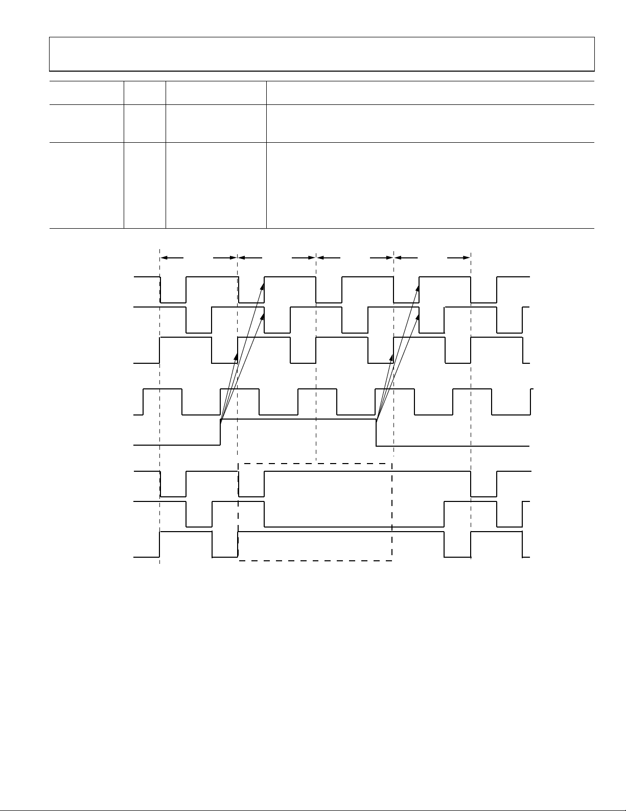
Figure 19 shows when the high speed clocks RG, H1 to H8, HL,
SHP, and SHD are generated. The RG pulse has programmable
rising and falling edges and can be inverted using the polarity
control. Horizontal Clock H1 has programmable rising and falling
edges and polarity control. In HCLK Mode 1, H3, H5, and H7
are equal to H1. H2, H4, H6, and H8 are always inverses of H1.
The edge location registers are each six bits wide, allowing the
selection of all 64 edge locations. Figure 23 shows the default
timing locations for all of the high speed clock signals.
...
t
CONV
t
= 6 ns TYP).
CLIDLY
06878-018
CCD
SIGNAL
RG
H1, H3, H5, H7
H2, H4, H6, H8
34
56
78
HL
PROGRAMMABLE CLOCK POSI T IONS:
1
SHP SAMPLE LO CAT I O N.
2
SHD SAMPLE LOCATION.
3
RG RISING EDGE.
4
RG FALLING EDGE.
5
H1 RISING EDGE.
6
H1 FALLING EDGE.
7
HL RISING EDGE.
8
HL FALLING EDGE.
2
6878-019
Figure 19. High Speed Clock Programmable Locations (HCLKMODE = 0x01)
Rev. B | Page 18 of 112
AD9920A
H-Driver and RG Outputs
In addition to the programmable timing positions, the AD9920A
features on-chip output drivers for the RG, HL, and H1 to H8
outputs. These drivers are powerful enough to drive the CCD
inputs directly. The H-driver and RG current can be adjusted for
optimum rise/fall time for a particular load by using the drive
strength control registers (Address 0x36 and Address 0x37). The
3-bit drive setting for each H1 to H8 output is adjustable in
4.3 mA increments: 0 = off, 1 = 4.3 mA, 2 = 8.6 mA, 3 = 12.9 mA,
4 = 17.3 mA, 5 = 21.6 mA, 6 = 25.9 mA, and 7 = 30.2 mA.
The 3-bit drive settings for the HL and RG outputs are also
adjustable in 4.3 mA increments, but with a maximum drive
strength of 17.3 mA: 0 = off, 1 = 4.3 mA, 2 = 8.6 mA, 3 = 12.9 mA,
4 = 4.3 mA, 5 = 8.6 mA, 6 = 12.9 mA, and 7 = 17.3 mA.
As shown in Figure 19, when HCLK Mode 1 is used, the H2,
H4, H6, and H8 outputs are inverses of the H1, H3, H5, and H7
outputs. Using the HCLKMODE register (Address 0x24,
Bits[4:0]), it is possible to select a different configuration.
Table 9. Timing Core Register Parameters for H1, H2, HL, RG, SHP, and SHD
Parameter Length (Bits) Range Description
Positive Edge 6 0 to 63 edge location Positive edge location for H1, H2, HL, H3P1, and RG.
Negative Edge 6 0 to 63 edge location Negative edge location for H1, H2, HL, H3P1, and RG.
Sampling Location 6 0 to 63 edge location Sampling location for internal SHP and SHD signals.
Drive Strength 3 0 to 7 current steps Drive current for H1 to H8, HL, and RG outputs (4.3 mA per step).
Tabl e 10 shows a comparison of the different programmable
settings for each HCLK mode. Figure 20 and Figure 21 show the
settings for HCLK Mode 2 and HCLK Mode 3, respectively.
It is recommended that all H1 to H8 outputs on the AD9920A be
used together for maximum flexibility in drive strength settings.
A typical CCD with H1 and H2 inputs should have only the
AD9920A H1, H3, H5, and H7 outputs connected together to
drive the CCD H1 and should have only the AD9920A H2, H4,
H6, and H8 outputs connected together to drive the CCD H2.
In 3-phase HCLK mode, only six of the HCLK outputs are used,
with two outputs driving each of the three phases:
• H1 and H2 are connected to CCD Phase 1.
• H5 and H6 are connected to CCD Phase 2.
• H7 and H8 are connected to CCD Phase 3.
Table 10. HCLK Modes, Selected by Address 0x24, Bits[4:0]
HCLKMODE Register Value Description
Mode 1 0x01 H1 edges are programmable with H3 = H5 = H7 = H1, H2 = H4 = H6 = H8 = inverse of H1.
Mode 2 0x02
Mode 3 0x04
3-Phase Mode 0x10 H1 edges are programmable using Address 0x33 and H2 = H1 (Phase 1).
H5 edges are programmable using Address 0x31 and H6 = H5 (Phase 2).
H7 edges are programmable using Address 0x30 and H8 = H7 (Phase 3).
Invalid Selection All other values Invalid register settings. Do not use.
H1 edges are programmable with H3 = H5 = H7 = H1.
H2 edges are programmable with H4 = H6 = H8 = H2.
H1 edges are programmable with H3 = H1 and H2 = H4 = inverse of H1.
H5 edges are programmable with H7 = H5 and H6 = H8 = inverse of H5.
Rev. B | Page 19 of 112
AD9920A
12
H1, H3, H5, H7
43
H2, H4, H6, H8
H1 TO H8 PROGRAMMABLE LOCATIONS:
1
H1 RISING EDGE.
2
H1 FALLING EDGE.
3
H2 RISING EDGE.
4
H2 FALLING EDGE.
Figure 20. HCLK Mode 2 Operation
12
H1, H3
H2, H4
34
H5, H7
H6, H8
H1 TO H8 PROGRAMMABLE LOCATIONS:
1
H1 RISING EDGE.
2
H1 FALLING EDGE.
3
H5 RISING EDGE.
4
H5 FALLING EDGE.
06878-021
Figure 21. HCLK Mode 3 Operation
H1, H2
1
2
06878-020
H5, H6
56
H7, H8
H1 TO H8 PROGRAMMABLE LOCATIONS:
1
H1 FALLING EDGE.
2
H1 RISI NG EDGE .
3
H5 FALLING EDGE.
4
H5 RISI NG EDGE .
5
H7 RISI NG EDGE .
6
H7 FALLING EDGE.
3
4
06878-022
Figure 22. 3-Phase HCLK Mode Operation
Rev. B | Page 20 of 112
AD9920A
CLI
RG
H1
H2
CCD
SIGNAL
SHP
SHD
DOUTPHASEP
NOTES
1. ALL SIGNAL EDGE S ARE FULLY PROGRAMMABLE TO ANY OF THE 64 POSITIONS WITHIN O NE PIXEL PE RIOD.
TYPICAL POSITIO NS FOR EACH S I G NAL ARE SHOWN. HCLK MODE 1 IS SHOWN.
2. CERTAIN PO SITIONS SHOULD BE AVOIDED FOR EACH SIGNAL, SHOWN ABOVE AS INHIBIT RE GIONS.
3. IF A SETTING IN THE INHIBIT REGION IS USED, AN UNSTABLE PIXEL SHIFT CAN OCCUR IN THE HBLK LO CATION OR AFE PIPELINE.
4. THE t
5. THE t
H1HBLK MASKING POLARITY.
6. THE t
P[0]
RGr[0] RGf[16]
H1r[0] H1f[32]
t
SHDINH
t
S2
SHDLOC[0]
1
t
DOUTINH
AREA FROM 50 TO 62 ONLY APPLIES IN SLAVE MODE.
SHPINH
AREA WILL APPLY TO EITHER H1 RISING OR FALLING EDGE, DEPENDING ON T HE VALUE OF THE
SHDINH
AREA CAN ALSO BE CHANGED TO A t
SHDINH
12
SHPINH
P[32]P[16] P[48]POSITION
t
S1
SHPLOC[32]
AREA IF THE H1HBLKRETI M E BIT = 1.
50
t
SHDINH
t
SHPINH
P[64] = P[0]
62
06878-023
Figure 23. High Speed Timing Default Locations
PHASE 1
P[0]
P[32]P[16] P[48]TAP POSITION
SHDINH/SHPINH
P[64] = P[0]
PHASE 2
PHASE 3
RGr[0] RGf[16]
RG
HLr[0] HLf[32]
HL
CCD
SIGNAL
SHP
SHDLOC[0]
SHD
NOTES
1. ALL SIGNAL EDGES ARE FULLY PROGRAMMABLE TO ANY OF THE 64 POSITIONS WITHIN ONE PIXEL PERIOD.
TYPICAL P OSITIONS FOR EACH SIGNAL ARE SHO WN USING 3-PHAS E HBLK MODE.
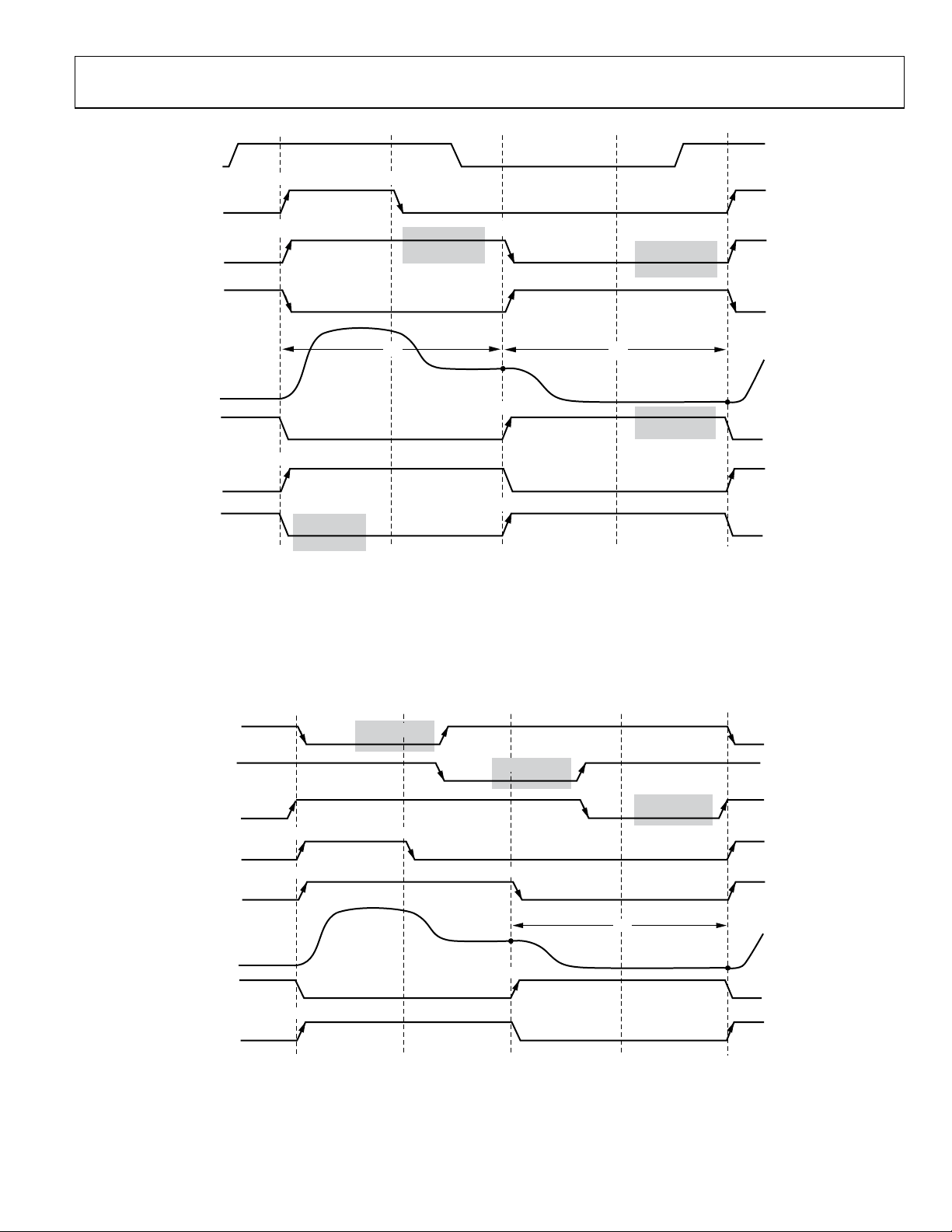
2. THE RISING EDGE O F EACH HCLK PHASE HAS AN ASSOCIATED SHDINH.
3. WHEN THE HBLK RETIME BITS (0x35 [3:0] ) ARE ENABLED, THE I NHIBITED AREA BECOMES SHPINH.
4. WHEN THE HBLK MASK LEVEL FOR PHASE 1, 2, OR 3 IS CHANGED TO L OW, THE INHIBIT AREA IS
REFERENCED TO THE HCLK FALLING EDGE, INSTEAD OF THE HCLK RISING EDGE.
Figure 24. High Speed Timing Typical Locations, 3-Phase HCLK Mode
SHDINH/SHPINH
SHPLOC[32]
SHDINH/SHPINH
t
S1
06878-024
Rev. B | Page 21 of 112
AD9920A
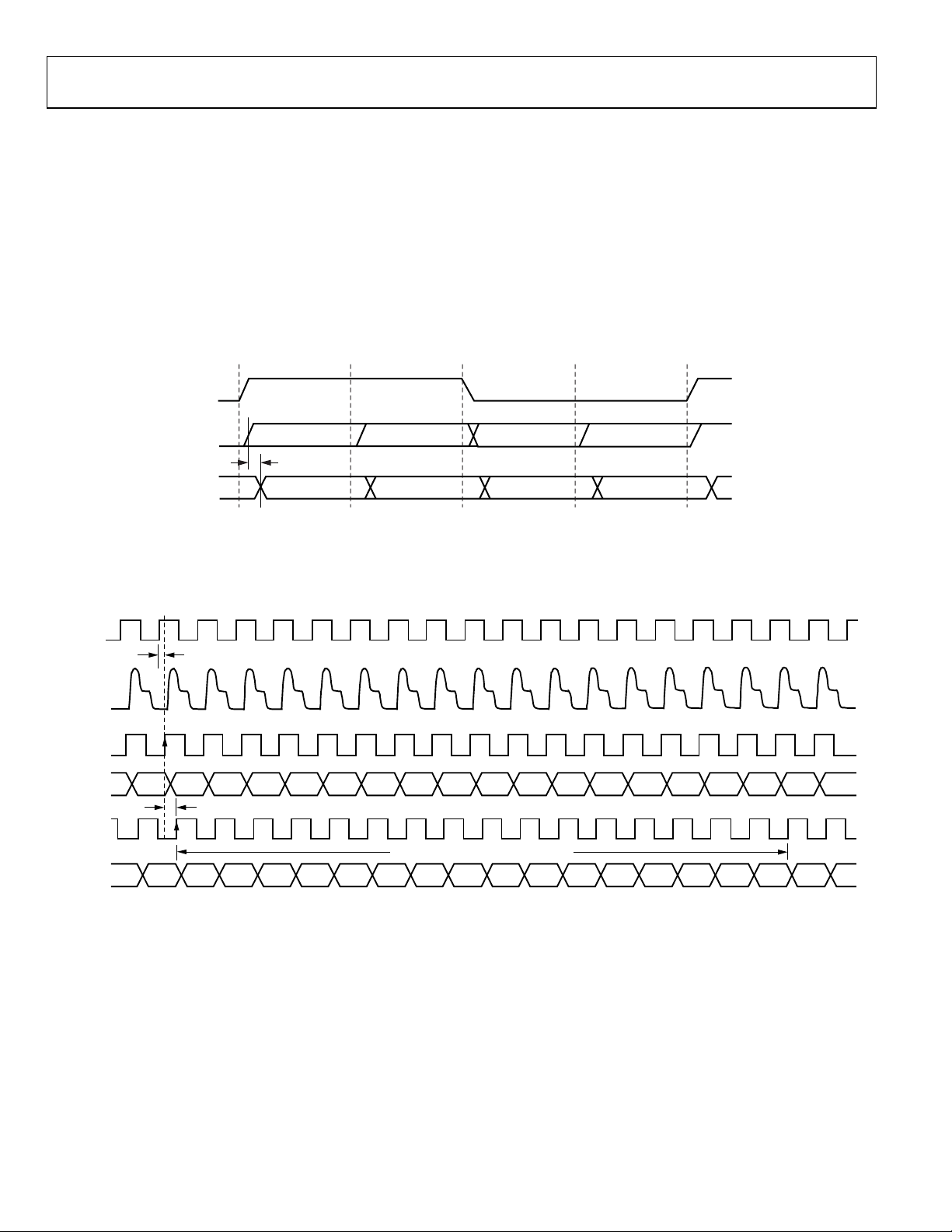
DIGITAL DATA OUTPUTS
The AD9920A data output and DCLK phase are programmable
using the DOUTPHASE registers (Address 0x39, Bits[13:0]).
DOUTPHASEP (Bits[5:0]) selects any edge location from 0 to
63, as shown in Figure 25. DOUTPHASEN (Bits[13:8]) does
not actually program the phase of the data outputs but is used
internally and should always be programmed to a value of
DOUTPHASEP plus 32 edges. For example, if DOUTPHASEP
is set to 0, DOUTPHASEN should be set to 32 (0x20).
P[0]
PIXEL
PERIOD
DCLK
t
OD
DOUT
NOTES
1. DATA OUTPUT (DOUT) AND DCL K P HAS E ARE ADJUSTABLE WITH RESPECT TO THE PIXEL PERIOD.
2. WITHIN ONE CLO CK PERIOD, T HE DAT A TRANSITI ON CAN BE PROGRAMMED TO 64 DIFFERENT LOCATIONS .
3. DCLK CAN BE INVERTED WITH RE S P E CT TO DOUT BY USING THE DCLKINV REGISTER.
Figure 25. Digital Output Phase Adjustment Using DOUTPHASEP Register
P[16]
Normally, the data output and DCLK signals track in phase,
based on the contents of the DOUTPHASE registers. The DCLK
output phase can also be held fixed with respect to the data outputs by setting the DCLKMODE register high (Address 0x39,
Bit 16). In this mode, the DCLK output remains at a fixed phase
equal to a delayed version of CLI, and the data output phase
remains programmable.
The pipeline delay through the AD9920A is shown in Figure 26.
After the CCD input is sampled by SHD, there is a 16-cycle
delay until the data is available.
P[32]
P[48]
P[64] = P[0]
06878-025
CCDIN
SHD
(INTERNAL)
ADC DOUT
(INTERNAL)
DCLK
DOUT
CLI
t
CLIDLY
NN + 2N + 1
SAMPLE PIXEL N
t
DOUTINH
NOTES
1. TIMING VALUES SHOWN ARE SHDLOC = 0, WITH DCLKMO DE = 0.
2. HIGHER VALUES OF SHD AND/OR DOUTPHASE SHIFT DOUT TRANSITION TO THE RIGHT, WITH RESPECT TO CLI LOCATION.
3. RECOMMENDED VALUE F O R DOUT P HASE I S TO USE SHPLOC OR UP TO 15 EDGES FOL LOWING SHPL O C.
N – 14 N – 4N – 5N – 6N – 7N – 8N – 9N – 10N – 11N – 12N – 13 N – 3 N – 2 N – 1 N N + 1N – 15N – 16N – 17
N + 3
N – 14 N – 4N – 5N – 6N – 7N – 8N – 9N – 10N – 11N – 12N – 13 N – 3 N – 2 N – 1 N N + 1N – 15N – 16N – 17
N + 4
PIPELINE LATENCY = 16 CYCLES
Figure 26. Digital Data Output Pipeline Delay
N + 13N + 12N + 11N + 10N + 9N + 8N + 7N + 6N + 5
N + 14
N + 16 N + 17N + 15
06878-026
Rev. B | Page 22 of 112

AD9920A
HORIZONTAL CLAMPING AND BLANKING
The horizontal clamping and blanking pulses of the AD9920A are
fully programmable to suit a variety of applications. Individual
control is provided for CLPOB, PBLK, and HBLK in the different
regions of each field. This allows the dark pixel clamping and
blanking patterns to be changed at each stage of the readout to
accommodate different image transfer timing and high speed
line shifts.
Individual CLPOB and PBLK Patterns
The AFE horizontal timing consists of CLPOB and PBLK, as
shown in Figure 27. These two signals are programmed independently using the registers shown in Tab le 1 1. The start polarity
for the CLPOB (or PBLK) signal is CLPOBPOL (PBLKPOL), and
the first and second toggle positions of the pulse are CLPOBTOG1
(PBLKTOG1) and CLPOBTOG2 (PBLKTOG2). Both signals
are active low and should be programmed accordingly.
A separate pattern for CLPOB and PBLK can be programmed
for each vertical sequence. As described in the Ver t ica l Tim i ng
Generation section, several V-sequences can be created, each
containing a unique pulse pattern for CLPOB and PBLK.
Figure 57 shows how the sequence change positions divide the
readout field into regions. By assigning a different V-sequence
to each region, the CLPOB and PBLK signals can change with
each change in the vertical timing.
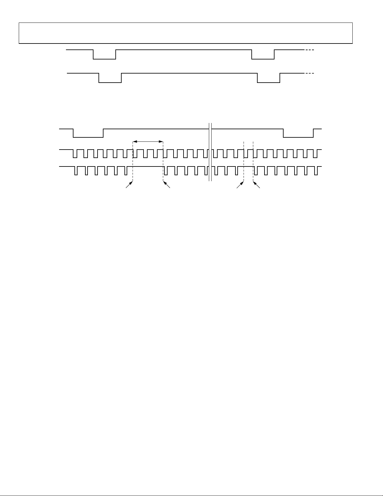
CLPOB and PBLK Masking Areas
Additionally, the AD9920A allows the CLPOB and PBLK signals
to be disabled in certain lines in the field without changing any
of the existing CLPOB pattern settings.
To use CLPOB (or PBLK) masking, the CLPMASKSTART
(PBLKMASKSTART) and CLPMASKEND (PBLKMASKEND)
registers are programmed to specify the start and end lines in
the field where the CLPOB (PBLK) patterns are ignored. The
three sets of start and end registers allow up to three CLPOB
(PBLK) masking areas to be created.
The CLPOB and PBLK masking registers are not specific to a
certain V-sequence; they are always active for any existing field
of timing. During operation, to disable the CLPOB masking
feature, these registers must be set to the maximum value of
0x1FFF or a value greater than the programmed VD length.
Note that to disable CLPOB (or PBLK) masking during power-up,
it is recommended that CLPMASKSTART (PBLKMASKSTART)
be set to 8191 and that CLPMASKEND (PBLKMASKEND) be
set to 0. This prevents any accidental masking caused by register
update events.
Table 11. CLPOB and PBLK Pattern Registers
Length
Register
CLPOBPOL 1 High/low Starting polarity of CLPOB for each V-sequence.
PBLKPOL 1 High/low Starting polarity of PBLK for each V-sequence.
CLPOBTOG1 13 0 to 8191 pixel location First CLPOB toggle position within line for each V-sequence.
CLPOBTOG2 13 0 to 8191 pixel location Second CLPOB toggle position within line for each V-sequence.
PBLKTOG1 13 0 to 8191 pixel location First PBLK toggle position within line for each V-sequence.
PBLKTOG2 13 0 to 8191 pixel location Second PBLK toggle position within line for each V-sequence.
CLPMASKSTART 13 0 to 8191 line location CLPOB masking area—starting line within field (maximum of three areas).
CLPMASKEND 13 0 to 8191 line location CLPOB masking area—ending line within field (maximum of three areas).
PBLKMASKSTART 13 0 to 8191 line location PBLK masking area—starting line within field (maximum of three areas).
PBLKMASKEND 13 0 to 8191 line location PBLK masking area—ending line within field (maximum of three areas).
(Bits)
Range Description
Rev. B | Page 23 of 112
AD9920A
HD
CLPOB
1
PBLK
PROGRAMMABL E S E TTINGS :
1
START POL ARITY (CLAMP AND BLANK REGION ARE ACT IVE LOW).
2
FIRST TOGGLE POSITION.
3
SECOND TOGGLE POSITION.
32
ACTIVE
Figure 27. Clamp and Preblank Pulse Placement
VD
0 1 2 597 598
HD
CLPOB
CLPMASKSTART1 = 6 CLPMASKEND1 = 9
NO CLPOB SI G NAL
FOR LINES 6 TO 8
Figure 28. CLPOB Masking Example
Individual HBLK Patterns
The HBLK programmable timing shown in Figure 29 is similar to
the timing of CLPOB and PBLK; however, there is no start polarity
control. Only the toggle positions are used to designate the start
and stop positions of the blanking period. Additionally, separate
masking polarity controls for each H-clock phase designate the
polarity of the horizontal clock signals during the blanking period.
Setting HBLKMASK_H1 high sets H1—and, therefore, H3, H5,
and H7—low during the blanking, as shown in Figure 30. As with
the CLPOB and PBLK signals, HBLK registers are available in
each V-sequence, allowing different blanking signals to be used
with different vertical timing sequences.
The AD9920A supports two modes of HBLK operation. HBLK
Mode 0 supports basic operation and pixel mixing HBLK operation. HBLK Mode 1 supports advanced HBLK operation.
The following sections describe each mode in detail. Register
parameters are described in detail in Ta b le 1 2 .
ACTIVE
06878-027
NO CLPOB SI GNAL
FOR LINE 600
CLPMASKSTART2 = 600 CLPMASKEND2 = 601
06878-028
HBLK Mode 0 Operation
There are six toggle positions available for HBLK. Normally, only
two of the toggle positions are used to generate the standard
HBLK interval. However, the additional toggle positions can be
used to generate special HBLK patterns, as shown in Figure 31.
The pattern in this example uses all six toggle positions to generate two extra groups of pulses during the HBLK interval. By
changing the toggle positions, different patterns can be created.
Separate toggle positions are available for even and odd lines. If
alternation is not needed, the same values should be loaded into
the registers for even (HBLKTOGE) and odd (HBLKTOGO) lines.
Multiple repeats of the HBLK signal are enabled by setting the
HBLKLEN and HBLKREP registers along with the six toggle
positions (four are shown in Figure 32).
Generating HBLK Line Alternation
HBLK Mode 0 provides the ability to alternate different HBLK
toggle positions on even and odd lines. HBLK line alternation
can be used alone or in conjunction with V-pattern odd/even
alternation (see the Generating Line Alternation for V-Sequences
and HBLK section). Separate toggle positions are available for
even and odd lines. If even/odd line alternation is not needed,
the same values should be loaded into the registers for even
(HBLKTOGE) and odd (HBLKTOGO) lines.
Rev. B | Page 24 of 112
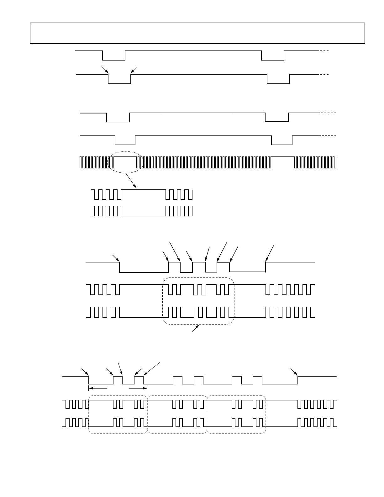
AD9920A
G
HD
HBLKSTART HBLKEND
HBLK
BLANK BLANK
BASIC HBLK PULSE IS GENERATED US ING HBLKSTART AND HBLKEND REGISTERS
06878-118
Figure 29. Typical Horizontal Blanking Pulse Placement (HBLK_MODE = 0)
HD
HBLK
H1/H3/H5/H7
THE POLARITY OF H1/H3/H5/H7 DURING BLANKING IS P ROGRAMMABLE
(H2/H4/H6/H8 AND HL ARE SEPARATELY PROGRAMMABL E)
H1/H3/H5/H7
H2/H4/H6/H8
6878-029
Figure 30. HBLK Masking Polarity Control
HBLKSTART
HBLKTOGE2
HBLKTOGE1 HBLKTOGE3
HBLKTO
HBLKTOGE4
E5
HBLKTOGE6
HBLKEND
HBLK
H1/H3
H2/H4
SPECIAL H-BL ANK P AT TERN IS CREATE D US ING MULTI PLE HBLK TO GGLE PO S ITIONS
06878-030
Figure 31. Using Multiple Toggle Positions for HBLK (HBLK_MODE = 0)
HBLKSTART HBLKTOGE1
HBLK
H1/H3
H2/H4
HBLKTOGE2
HBLKLEN
HBLKREP = 3
HBLKREP NUMBER 1 HBLKREP NUMBER 2 HBLKREP NUMBER 3
H-BLANK REPEATING PATTERN IS CREATED USING HBLKLE N AND HBLKREP REGISTERS
HBLKTOGE4
Figure 32. HBLK Repeating Pattern Using HBLK_MODE = 0
HBLKENDHBLKTOGE3
06878-031
Rev. B | Page 25 of 112

AD9920A
Table 12. HBLK Pattern Registers
Length
Register
HBLK_MODE 2 0 to 1 HBLK modes Enables different HBLK toggle position operations.
2 = test mode only; do not access.
3 = test mode only; do not access.
HBLKSTART 13 0 to 8191 pixel location Start location for HBLK in HBLK Mode 0 and HBLK Mode 1.
HBLKEND 13 0 to 8191 pixel location End location for HBLK in HBLK Mode 0 and HBLK Mode 1.
HBLKLEN 13 0 to 8191 pixels HBLK length in HBLK Mode 0 and HBLK Mode 1.
HBLKREP 13 0 to 8191 repetitions Number of HBLK repetitions in HBLK Mode 0 and HBLK Mode 1.
HBLKMASK_H1 1 High/low Masking polarity for H1/H3/H5/H7 during HBLK.
HBLKMASK_H2 1 High/low Masking polarity for H2/H4/H6/H8 during HBLK.
HBLKMASK_HL 1 High/low Masking polarity for HL during HBLK.
HBLKMASK_H3P 1 High/low Masking polarity for H3P during 3-phase mode during HBLK.
HBLKTOGO1 13 0 to 8191 pixel location First HBLK toggle position for odd lines in HBLK Mode 0.
HBLKTOGO2 13 0 to 8191 pixel location Second HBLK toggle position for odd lines in HBLK Mode 0.
HBLKTOGO3 13 0 to 8191 pixel location Third HBLK toggle position for odd lines in HBLK Mode 0.
HBLKTOGO4 13 0 to 8191 pixel location Fourth HBLK toggle position for odd lines in HBLK Mode 0.
HBLKTOGO5 13 0 to 8191 pixel location Fifth HBLK toggle position for odd lines in HBLK Mode 0.
HBLKTOGO6 13 0 to 8191 pixel location Sixth HBLK toggle position for odd lines in HBLK Mode 0.
HBLKTOGE1 13 0 to 8191 pixel location First HBLK toggle position for even lines in HBLK Mode 0.
HBLKTOGE2 13 0 to 8191 pixel location Second HBLK toggle position for even lines in HBLK Mode 0.
HBLKTOGE3 13 0 to 8191 pixel location Third HBLK toggle position for even lines in HBLK Mode 0.
HBLKTOGE4 13 0 to 8191 pixel location Fourth HBLK toggle position for even lines in HBLK Mode 0.
HBLKTOGE5 13 0 to 8191 pixel location Fifth HBLK toggle position for even lines in HBLK Mode 0.
HBLKTOGE6 13 0 to 8191 pixel location Sixth HBLK toggle position for even lines in HBLK Mode 0.
RA0H1REPA/B/C 12
RA1H1REPA/B/C 12 0 to 15 HCLK pulses HBLK Repeat Area 1. Number of H1 repetitions for HBLKSTARTA/B/C.
RA2H1REPA/B/C 12 0 to 15 HCLK pulses HBLK Repeat Area 2. Number of H1 repetitions for HBLKSTARTA/B/C.
RA3H1REPA/B/C 12 0 to 15 HCLK pulses HBLK Repeat Area 3. Number of H1 repetitions for HBLKSTARTA/B/C.
RA4H1REPA/B/C 12 0 to 15 HCLK pulses HBLK Repeat Area 4. Number of H1 repetitions for HBLKSTARTA/B/C.
RA5H1REPA/B/C 12 0 to 15 HCLK pulses HBLK Repeat Area 5. Number of H1 repetitions for HBLKSTARTA/B/C.
RA0H2REPA/B/C 12
RA1H2REPA/B/C 12 0 to 15 HCLK pulses HBLK Repeat Area 1. Number of H2 repetitions for HBLKSTARTA/B/C.
RA2H2REPA/B/C 12 0 to 15 HCLK pulses HBLK Repeat Area 2. Number of H2 repetitions for HBLKSTARTA/B/C.
RA3H2REPA/B/C 12 0 to 15 HCLK pulses HBLK Repeat Area 3. Number of H2 repetitions for HBLKSTARTA/B/C.
RA4H2REPA/B/C 12 0 to 15 HCLK pulses HBLK Repeat Area 4. Number of H2 repetitions for HBLKSTARTA/B/C.
RA5H2REPA/B/C 12 0 to 15 HCLK pulses HBLK Repeat Area 5. Number of H2 repetitions for HBLKSTARTA/B/C.
(Bits) Range Description
0 = normal mode; six toggle positions available for even and odd lines.
If even/odd alternation is not needed, set toggles for even and odd lines to the
same value. In addition to the six toggle positions, the HBLKSTART, HBLKEND,
HBLKLEN, and HBLKREP registers can be used to generate HBLK patterns. If even/
odd alternation is not needed, set toggles for even and odd lines to the same value.
1 = advanced HBLK mode; divides HBLK interval into six repeat areas.
Uses HBLKSTARTA/B/C and RAxHxREPA/B/C registers; the latter, depending on the
mode of operation, are stored in the HBLKTOGO1 to HBLKTOGO6 and HBLKTOGE1
to HBLKTOGE6 registers (Address 0x19 to Address 0x1E; see Table 63).
0 to 15 HCLK pulses for
each A, B, and C
0 to 15 HCLK pulses for
each A, B, and C
HBLK Repeat Area 0. Number of H1 repetitions for HBLKSTARTA/B/C in
HBLK Mode 1 for even lines; odd lines defined using HBLKALT_PAT.
Bits[3:0]: RA0H1REPA. Number of H1 pulses following HBLKSTARTA.
Bits[7:4]: RA0H1REPB. Number of H1 pulses following HBLKSTARTB.
Bits[11:8]: RA0H1REPC. Number of H1 pulses following HBLKSTARTC.
HBLK Repeat Area 0. Number of H2 repetitions for HBLKSTARTA/B/C in
HBLK Mode 1 for even lines; odd lines defined using HBLKALT_PAT.
Bits[3:0]: RA0H2REPA. Number of H2 pulses following HBLKSTARTA.
Bits[7:4]: RA0H2REPB. Number of H2 pulses following HBLKSTARTB.
Bits[11:8]: RA0H2REPC. Number of H2 pulses following HBLKSTARTC.
Rev. B | Page 26 of 112
AD9920A
Length
Register
HBLKSTARTA 13 0 to 8191 pixel location HBLK Repeat Area Start Position A for HBLK Mode 1. Set to 8191 if not used.
HBLKSTARTB 13 0 to 8191 pixel location HBLK Repeat Area Start Position B for HBLK Mode 1. Set to 8191 if not used.
HBLKSTARTC 13 0 to 8191 pixel location HBLK Repeat Area Start Position C for HBLK Mode 1. Set to 8191 if not used.
HBLKALT_PAT0 3 0 to 5 even repeat area
HBLKALT_PAT1 3 0 to 5 even repeat area HBLK Mode 1, Repeat Area 1 pattern for odd lines.
HBLKALT_PAT2 3 0 to 5 even repeat area HBLK Mode 1, Repeat Area 2 pattern for odd lines.
HBLKALT_PAT3 3 0 to 5 even repeat area HBLK Mode 1, Repeat Area 3 pattern for odd lines.
HBLKALT_PAT4 3 0 to 5 even repeat area HBLK Mode 1, Repeat Area 4 pattern for odd lines.
HBLKALT_PAT5 3 0 to 5 even repeat area HBLK Mode 1, Repeat Area 5 pattern for odd lines.
(Bits) Range Description
HBLK Mode 1, Repeat Area 0 pattern for odd lines. Selected from previously
defined even line repeat areas.
PHASE 1
PHASE 2
PHASE 3
INTERNAL
DIGITAL
CLOCK
MASTER
BLANKING
SIGNAL
H1/H2
H5/H6
H7/H8
1 PIXEL
A3
A
1 PIXEL 1 PIXEL 1 PIXEL
A1
A2
MASK LEVEL = HIGH
MASK LEVEL = LOW
MASK LEVEL = HIGH
Figure 33. Example of Correct HBLK Behavior
HBLK Fine Retime Control
An additional set of register bits is available for use during
3-phase HCLK mode to provide fine adjustment of each HCLK
phase during the HBLK interval. The fine retime bits (Address 0x35,
Bits[23:20]) allow for the adjustment of the correct number of
HCLK cycles during the HBLK interval.
Figure 33 through Figure 35 show the different settings that can
be used based on the location of the HBLK toggle positions, the
location of the internal digital clock, and the masking polarity
of the different HCLK phases. By using the fine retime bits, the
exact pulse behavior for each HCLK phase can be generated.
Rev. B | Page 27 of 112
BLANKING
B1
B2
B3
B
06878-032
Figure 33 shows the desired HBLK behavior for all three phases
when the internal digital clock is located before the Phase 3 rising
edge. Figure 34 shows the effect of changing the internal clock
phase (changing SHDLOC) to a different location. This causes
incorrect blanking on Phase 1 and Phase 2.
Figure 35 shows how the fine retime bits for Phase 1 and Phase 2
are used to generate the correct blanking behavior, matching the
result shown in Figure 33.
AD9920A
1 PIXEL 1 PIXEL1 PIXEL1 PIXEL1 P IXEL
PHASE 1
PHASE 2
PHASE 3
INTERNAL
DIGITAL
CLOCK
MASTER
BLANKING
SIGNAL
H1/H2
H5/H6
H7/H8
A1
A2
A3
A
MASK LEVEL = HIGH
MASK LEVEL = LOW
MASK LEVEL = HIGH
BLANKING
B1
B2
B3
B
06878-033
Figure 34. Incorrect HBLK Behavior Caused by Internal Clock Position
1 PIXEL 1 PIXEL1 PIXEL1 PIXEL1 PIXEL
FINE RET I ME
PHASE 1
PHASE 2
A2
PHASE 3
INTERNAL
DIGITAL
CLOCK
MASTER
BLANKING
SIGNAL
H1/H2
H5/H6
H7/H8
A
A1
FINE RET I ME
FINE RETIME
A3
MASK LEVEL = HIGH
MASK LEVEL = LOW
MASK LEVEL = HIGH
BLANKING
Figure 35. Fine Retime on Phase 2 to Achieve Correct HBLK
B1
FINE RET IME
B2
B3
B
6878-034
Rev. B | Page 28 of 112
AD9920A
Increasing H-Clock Width During HBLK
The AD9920A allows the H1 to H8 pulse width to be increased
during the HBLK interval. As shown in Figure 36, the H-clock frequency can be reduced by a factor of 1/2, 1/4, 1/6, 1/8, 1/10, 1/12,
and so on, up to 1/30. To enable this feature, the HCLK_WIDTH
register (Address 0x35, Bits[7:4]) is set to a value between 1 and 15.
When this register is set to 0, the wide HCLK feature is disabled.
The reduced frequency occurs for only the H1 to H8 pulses that
are located within the HBLK area.
The HCLK_WIDTH register is generally used in conjunction
with special HBLK patterns to generate vertical and horizontal
mixing in the CCD.
Table 13. HCLK Width Register
Register Length (Bits) Description
HCLK_WIDTH 4 Controls the H1 to H8 pulse widths during HBLK as a fraction of pixel rate
0 = same frequency as pixel rate; 1 = 1/2 pixel frequency (doubles the HCLK pulse width);
2 = 1/4 pixel frequency; 3 = 1/6 pixel frequency; 4 = 1/8 pixel frequency;
5 = 1/10 pixel frequency; 15 = 1/30 pixel frequency
HBLK Mode 1 Operation
HBLK Mode 1 allows more advanced HBLK pattern operation.
If multiple areas of HCLK pulses that are unevenly spaced from
one another are needed, HBLK Mode 1 can be used. Using a
separate set of registers, HBLK Mode 1 can divide the HBLK
region into up to six repeat areas (see Ta b le 1 2).
As shown in Figure 37, each repeat area shares a common
group of toggle positions: HBLKSTARTA, HBLKSTARTB, and
HBLKSTARTC. However, the number of toggles following a start
position can be unique in each repeat area by using the RAxH1REP
and RAxH2REP registers; these registers, depending on the mode
of operation, are stored in the HBLKTOGO1 to HBLKTOGO6
and HBLKTOGE1 to HBLKTOGE6 registers (Address 0x19 to
Address 0x1E; see Tab le 6 3 ).
HBLK
H1/H3
H2/H4
1/f
PIX
H-CLOCK FREQUENCY CAN BE REDUCED DURING HBLK BY 1/2 (AS SHO WN),
1/4, 1/6, 1/8, 1/10, 1/12, AND SO ON, UP TO 1/30 USIN G HBLK_WI DTH REGISTER.
2 × (1/f
)
PIX
06878-035
Figure 36. Generating Wide H-Clock Pulses During HBLK Interval
HD
H1
H2
CREATE UP TO THREE GROUPS OF TOG GLES
(A, B, C) COMMON IN ALL REP EAT AREAS
A
B
C
HBLKSTART
REPEAT AREA 0
REPEAT AREA 1 REPEAT AREA 2
MASK A, B, C PULS E S IN ANY REPEAT
AREA BY SETTI N G RAxHxREPx = 0
REPEAT AREA 3
Figure 37. HBLK Mode 1 Registers
CHANGE NUMBER OF A, B, C PULSES IN ANY
REPEAT AREA USING RAxHxREPx REGISTERS
REPEAT AREA 4 REPEAT AREA 5
HBLKEND
06878-036
Rev. B | Page 29 of 112
AD9920A
K
HD
HBLKLEN
HBL
HBLKSTARTA
HBLKSTARTB
HBLKSTARTC
H1
RA0H1REPA
H2
HBLKSTART
RA0H2REPA
RA0H1REPB RA0H1REPC
RA0H2REPB RA0H2REPC
REPEAT AREA 0
TO CREATE TWO REPEAT ARE AS
ALL RAxHxREPA/B/C REGISTERS = 2 TO CREATE TWO HCLK PULSE S
HBLKREP = 2
Figure 38. HBLK Mode 1 Operation
As shown in Figure 38, setting the RAxH1REPA/B/C or
RAxH2REPA/B/C register to 0 masks HCLK groups from
appearing in a particular repeat area. Figure 37 shows only two
repeat areas being used, although six are available. It is possible
to program a separate number of repeat area repetitions for H1
and H2, but generally the same value is used for both H1 and
H2. Figure 37 shows an example of RA0H1REPA/B/C =
RA0H2REPA/B/C = RA1H1REPA/B/C = RA1H2REPA/B/C = 2.
Furthermore, HBLK Mode 1 allows a different HBLK pattern on
even and odd lines. The HBLKSTARTA/B/C registers, as well as
the RAxH1REPA/B/C and RAxH2REPA/B/C registers, define
operation for the even lines. For separate control of the odd lines,
the HBLKALT_PAT registers specify up to six repeat areas on
the odd lines by reordering the repeat areas used for the even
lines. New patterns are not available, but the order of the previously defined repeat areas on the even lines can be changed
for the odd lines to accommodate advanced CCD operation.
HORIZONTAL TIMING SEQUENCE EXAMPLE
Figure 39 shows an example CCD layout. The horizontal register
contains 28 dummy pixels that occur on each line clocked from
the CCD. In the vertical direction, there are 10 optical black
(OB) lines at the front of the readout and two at the back of the
readout. The horizontal direction has four OB pixels in the
front and 48 OB pixels in the back.
RA1H1REPA
RA1H2REPA
RA1H1REPB RA1H1REPC
RA1H2REPB RA1H2REPC
REPEATAREA 1
HBLKEND
Figure 40 shows the basic sequence to be used during the
effective pixel readout. The 48 OB pixels at the end of each line
are used for the CLPOB signals. PBLK is optional and is often
used to blank the digital outputs during the HBLK time. HBLK
is used during the vertical shift interval.
Because PBLK is used to isolate the CDS input (see the Analog
Preblanking section), the PBLK signal should not be used
during CLPOB operation. The change in the offset behavior
that occurs during PBLK affects the accuracy of the CLPOB
circuitry.
The HBLK, CLPOB, and PBLK parameters are programmed
in the V-sequence registers. More elaborate clamping schemes,
such as adding a separate sequence to clamp in the entire shield
OB lines, can be used. This requires configuring a separate
V-sequence for clocking out the OB lines.
The CLPMASK registers are also useful for disabling the CLPOB
on a few lines without affecting the setup of the clamping
sequences. It is important that CLPOB be used only during
valid OB pixels. During other portions on the frame timing,
such as vertical blanking or SG line timing, the CCD does not
output valid OB pixels. Any CLPOB pulse that occurs during
this time causes errors in clamping operation and changes in
the black level of the image.
06878-037
Rev. B | Page 30 of 112

AD9920A
V
T
C
2 VERTICAL
OB LINES
V
4 OB PIXELS
EFFECTIVE IMAGE AREA
H
HORIZONTAL CCD REGISTER
48 OB PIXE LS
10 VERTICAL
OB LINES
CD OUTP UT
SHP
SHD
H1/H3/H5/H7
H2/H4/H6/H8
HBLK
PBLK
CLPOB
28 DUMMY PI XELS
Figure 39. Example CCD Configuration
OPTICAL BLACK
HD
VERTICAL SHIFT
NOTES
1. PBLK ACTIVE (LOW) SHOULD NOT BE US E D DURING CLPOB ACT IVE (LO W).
OPTICAL BLACK
DUMMY EFF ECTIVE PIXELS
Figure 40. Horizontal Sequence Example
06878-038
OPTICAL BL ACK
ERTICAL SHIF
6878-039
Rev. B | Page 31 of 112

AD9920A
VERTICAL TIMING GENERATION
The AD9920A provides a flexible solution for generating vertical
CCD timing and can support multiple CCDs and different system
architectures. The vertical transfer clocks are used to shift each
line of pixels into the horizontal output register of the CCD. The
AD9920A allows these outputs to be individually programmed
into various readout configurations by using a four-step process.
Figure 41 shows an overview of how the vertical timing is
generated in four steps.
1. The individual pulse patterns for XV1 to XV24 are created
by using the vertical pattern group registers.
CREATE THE VE RT ICAL PATT E RN GROUPS,
1 2
UP TO FO UR TOGGL E POSITIONS FOR E ACH OUTPUT.
XV1
XV2
XV3
VPAT0
XV23
XV24
XV1
XV2
XV3
VPAT1
XV23
XV24
2. The V-pattern groups are used to build the V-sequences
where additional information is added.
3. The readout for an entire field is constructed by dividing
the field into regions and then assigning a sequence to each
region. Each field can contain up to nine different regions
to accommodate the various steps of the readout, such as
high speed line shifts and unique vertical line transfers.
The total number of V-patterns, V-sequences, and fields is
programmable but limited by the number of registers.
4. The mode registers allow the different fields to be combined
in any order for various readout configurations.
BUILD THE V-SEQUENCES BY ADDING S TART POLARITY,
LINE START POSIT ION, NUMBER OF REPEATS , ALTERNATION,
GROUP A/B/C/D INFORMATIO N, AND HBLK/CLPOB PULSES.
XV1
XV2
V-SEQUENCE 0
(VPAT0, 1 REP)
V-SEQUENCE 1
(VPAT1, 2 REP)
V-SEQUENCE 2
(VPAT1, N REP )
XV3
XV23
XV24
XV1
XV2
XV3
XV23
XV24
XV1
XV2
XV3
XV23
XV24
USE THE MODE RE GISTERS TO CONTROL WHICH F IELDS
ARE USED AND IN WHAT ORDER (MAXI M UM OF SEVEN
FIELDS CAN BE COMBINED IN ANY ORDER).
FIELD1
FIELD3
FIELD5
FIELD2 FIELD3
FIELD4
FIELD1 FIELD4
FIELD2
BUILD EACH FI E L D BY DIVIDING INTO DIF FERENT REGIONS
34
AND ASSIGNING A DIFFERENT V-SEQ UEN CE T O EACH
(MAXIMUM O F NINE REGI ONS IN EACH FI E LD).
FIELD1
REGION 0: US E V -S E QUENCE 2
REGION 0: USE V-SEQUENCE 3
REGION 1: US E V -S E QUENCE 0
REGION 2: US E V -S E QUENCE 3
REGION 3: US E V -S E QUENCE 0
REGION 4: US E V -S E QUENCE 2
FIELD2
FIELD3
REGION 0: USE V-SEQUE NCE 3
REGION 1: US E V-SEQUE NCE 2
REGION 1: US E V-SEQU ENCE 2
REGION 2: US E V-SEQUE NCE 1
REGION 2: US E V-SEQU ENCE 1
06878-040
Figure 41. Summary of Vertical Timing Generation
Rev. B | Page 32 of 112

AD9920A
Vertical Pattern Groups (VPAT)
The vertical pattern groups define the individual pulse patterns
for each XV1 to XV24 output signal. Tab l e 14 summarizes the
registers available for generating each V-pattern group. The first,
second, third, and fourth toggle positions (VTOG1, VTOG2,
VTOG3, and VTOG4) are the pixel locations within the line
where the pulse transitions. All toggle positions are 13-bit
values, allowing their placement anywhere in the first 8191
pixels of the line.
More registers are included in the vertical sequence registers to
specify the output pulses. VPOL specifies the start polarity for
each signal; VSTART specifies the start position of the V-pattern
group within the line; VLEN designates the total length of the
V-pattern group, which determines the number of pixels between
each of the pattern repetitions when repetitions are used.
Table 14. Vertical Pattern Group Registers
Register Length (Bits) Description
VTOG1 13 First toggle position within the line for each XV1 to XV24 output, relative to VSTART value.
VTOG2 13 Second toggle position, relative to VSTART value.
VTOG3 13 Third toggle position, relative to VSTART value.
VTOG4 13 Fourth toggle position, relative to VSTART value.
START POSITION OF VERTICAL PATTERN GROUP IS PROGRAMMABLE IN VERTICAL SEQUENCE REGISTERS.
The VSTART position is actually an offset value for each toggle
position. The actual pixel location for each toggle, measured
from the HD falling edge (Pixel 0), is equal to the VSTART
value plus the toggle position.
When the selected V-output is designated as a VSG pulse, either
the VTOG1/VTOG2 or VTOG3/VTOG4 pair is selected using
V-Sequence Address 0x03, VSGPATSEL. All four toggle positions
are not simultaneously available for VSG pulses.
All unused V-channels must have their toggle positions
programmed to either 0 or maximum value. This prevents
unpredictable behavior because the default values of the
V-pattern group registers are unknown.
HD
4
XV1
XV2
XV24
PROGRAMMABLE SETTINGS:
1
START POLARITY (LOCATED IN V-SEQUENCE REGISTERS).
2
FIRST TOGGLE POSITIO N.
3
SECOND TOGGLE POSITION (THIRD AND FOURTH TOGGLE POSITIONS ALSO AVAI LABLE FOR M ORE COMPLE X P ATTERNS).
4
TOTAL P ATTERN LENG T H FOR ALL VE RTICAL OUT P UTS (LOCAT E D IN VERTICAL S EQUENCE REGIS TERS).
1
2
3
1
23
1
2
Figure 42. Vertical Pattern Group Programmability
3
06878-041
Rev. B | Page 33 of 112

AD9920A
X
VERTICAL SEQUENCES (VSEQ)
The vertical sequences are created by selecting one of the V-pattern
groups and adding repeats, start position, horizontal clamping, and
blanking information. The V-sequences are programmed using
the registers shown in Tabl e 15 . Figure 43 shows an example of
how these registers are used to generate the V-sequences.
The VPATSELA, VPATSELB, VPATSELC, and VPATSELD
registers select which V-pattern is used in a given V-sequence.
Having four groups available allows each vertical output to be
mapped to a different V-pattern. The user can add repetitions to
the selected V-pattern group for high speed line shifts or for line
binning by using the VREP registers for odd and even lines.
1
HD
3
V1 TO XV24
V-PATTERN GROUP
VREPA_ 2
44
Generally, the same number of repetitions is programmed into
both registers. If a different number of repetitions is required on
odd and even lines, separate values can be used for each register
(see the Generating Line Alternation for V-Sequences and HBLK
section). The VSTARTA, VSTARTB, VSTARTC, and VSTARTD
registers specify where in the line the V-pattern group starts.
The VMASK_EVEN and VMASK_ODD registers are used in
conjunction with the FREEZE/RESUME registers to enable
optional masking of the V-outputs. One or more of the
FREEZE1/RESUME1, FREEZE2/RESUME2, FREEZE3/
RESUME3, and FREEZE4/RESUME4 registers can be enabled.
The line length (in pixels) is programmable using the HDLEN
registers. Each V-sequence can have a different line length to
accommodate various image readout techniques. The maximum
number of pixels per line is 8192. The last line of the field is
programmed separately using the HDLASTLEN register, which
is located in the field register section (see Tabl e 64).
2
VREPA_3
CLPOB
HBLK
5
6
PROGRAMMABLE S E TTINGS F OR EACH VERTICAL SEQUENCE:
1
START POSITION IN THE LINE OF THE SELECTED V-PATTERN GROUP.
2
HD LINE LENG TH.
3
V-PATTERN SELECT (VPATSEL) TO SELECT ANY V-PATTERN GROUP.
4
NUMBER OF REPETITIONS OF THE V-PATTERN GROUP (IF NEEDED).
5
START POLARITY AND TOGGLE POSITIONS FOR CLPOB AND PBLK SIGNALS.
6
MASKING POLARITY AND TO GGLE POSITIONS FOR HBLK S IGNAL.
06878-042
Figure 43. V-Sequence Programmability
Rev. B | Page 34 of 112

AD9920A
Table 15. Summary of V-Sequence Registers (see Table 11 and Table 12 for the CLPOB, PBLK, and HBLK Register Summary)
Length
Register
HOLD 4
CONCAT_GRP 4
0 = disable.
1 = enable the addition of all toggle positions from VPATSELA/B/C/D.
2 to 15 = test mode only; do not use.
VREP_MODE 2
0 = disable alternation. Group A uses VREPA_1, Groups B/C/D use VREP_EVEN for all lines.
1 = two-line. Group A alternates VREPA_1 and VREPA_2. Groups B/C/D alternate VREP_EVEN and VREP_ODD.
LASTREPLEN_EN 4
HDLENE 14 HD line length for even lines in the V-sequence.
HDLENO 14 HD line length for odd lines in the V-sequence.
VPOL 24 Group A start polarity bits for each XV1 to XV24 signal.
GROUPSEL_0 24
0 = assign to Group A.
GROUPSEL_1 24
0 = assign to Group A.
VPATSELA 5 Selected V-pattern for Group A.
VPATSELB 5 Selected V-pattern for Group B.
VPATSELC 5 Selected V-pattern for Group C.
VPATSELD 5 Selected V-pattern for Group D.
VSTARTA 13 Start position for the selected V-pattern Group A.
VSTARTB 13 Start position for the selected V-pattern Group B.
VSTARTC 13 Start position for the selected V-pattern Group C.
VSTARTD 13 Start position for the selected V-pattern Group D.
VLENA 13 Length of selected V-pattern Group A.
VLENB 13 Length of selected V-pattern Group B.
VLENC 13 Length of selected V-pattern Group C.
VLEND 13 Length of selected V-pattern Group D.
VREPA_1 13 Number of repetitions for the V-pattern Group A for first lines (even).
VREPA_2 13 Number of repetitions for the V-pattern Group A for second lines (odd).
VREPA_3 13 Number of repetitions for the V-pattern Group A for third lines.
VREPA_4 13 Number of repetitions for the V-pattern Group A for fourth lines.
(Bits) Description
Use in conjunction with VMASK_EVEN and VMASK_ODD.
1 = Enable HOLD function instead of FREEZE/RESUME function.
Combines toggle positions of Group A, Group B, Group C, and Group D when enabled. Only Group A settings
for start, polarity, length, and repetition are used when this mode is selected.
Selects line alternation for V-output repetitions. Two separate controls: one for Group A and the other for
Group B, Group C, and Group D.
2 = three-line. Group A alternates VREPA_1, VREPA_2, and VREPA_3. Groups B/C/D follow a VREP_EVEN,
VREP_ODD, VREP_ODD, VREP_EVEN, VREP_ODD, VREP_ODD pattern.
3 = four-line. Group A alternates VREPA_1, VREPA_2, VREPA_3, and VREPA_4. Groups B/C/D follow two-line
alternation.
Enable a separate pattern length to be used during the last repetition of the V-sequence. One bit for each
group (A, B, C, and D); Group A is the LSB. Set bit high to enable. Recommended value is enabled.
Assigns each XV1 to XV12 signal to Group A, Group B, Group C, or Group D. Two bits for each signal.
Bits[1:0] are for XV1.
Bits[3:2] are for XV2.
Bits[23:22] are for XV12.
1 = assign to Group B.
2 = assign to Group C.
3 = assign to Group D.
Assigns each XV13 to XV24 signal to Group A, Group B, Group C, or Group D. Two bits for each signal.
Bits[1:0] are for XV13.
Bits[3:2] are for XV14.
Bits[23:22] are for XV24.
1 = assign to Group B.
2 = assign to Group C.
3 = assign to Group D.
Rev. B | Page 35 of 112

AD9920A
Length
Register
VREPB_ODD 13 Number of repetitions for the V-pattern Group B for odd lines.
VREPC_ODD 13 Number of repetitions for the V-pattern Group C for odd lines.
VREPD_ODD 13 Number of repetitions for the V-pattern Group D for odd lines.
VREPB_EVEN 13 Number of repetitions for the V-pattern Group B for even lines.
VREPC_EVEN 13 Number of repetitions for the V-pattern Group C for even lines.
VREPD_EVEN 13 Number of repetitions for the V-pattern Group D for even lines.
FREEZE1 13
FREEZE2 13
FREEZE3 13
FREEZE4 13
RESUME1 13
RESUME2 13
RESUME3 13
RESUME4 13
LASTREPLEN_A 13
LASTREPLEN_B 13
LASTREPLEN_C 13
LASTREPLEN_D 13
VSEQALT_EN 1 Special V-sequence alternation mode is enabled when this register is programmed high.
VALTSEL0_EVEN 18
VALTSEL1_EVEN 18
VALTSEL0_ODD 18
VALTSEL1_ODD 18
SPC_PAT_EN 3
SEQ_ALT_INC 1 0 = normal operation.
SEQ_ALT_RST 1 0 = normal operation.
(Bits) Description
Pixel location where the V-outputs freeze or hold (see VMASK_EVEN and VMASK_ODD). Also used as
VALTSEL0_EVEN, Bits[12:0] register when special VSEQALT_EN mode is enabled.
Pixel location where the V-outputs freeze or hold (see VMASK_EVEN and VMASK_ODD). Also used as
VALTSEL1_EVEN, Bits[12:0] register when special VSEQALT_EN mode is enabled.
Pixel location where the V-outputs freeze or hold (see VMASK_EVEN and VMASK_ODD). Also used as
VALTSEL0_ODD, Bits[12:0] register when special VSEQALT_EN mode is enabled.
Pixel location where the V-outputs freeze or hold (see VMASK_EVEN and VMASK_ODD). Also used as
VALTSEL1_ODD, Bits[12:0] register when special VSEQALT_EN mode is enabled.
Pixel location where the V-outputs resume operation (see VMASK_EVEN and VMASK_ODD). Also used as
VALTSEL0_EVEN, Bits[17:13] register when special VSEQALT_EN mode is enabled.
Pixel location where the V-outputs resume operation (see VMASK_EVEN and VMASK_ODD). Also used as
VALTSEL1_EVEN, Bits[17:13] register when special VSEQALT_EN mode is enabled.
Pixel location where the V-outputs resume operation (see VMASK_EVEN and VMASK_ODD). Also used as
VALTSEL0_ODD, Bits[17:13] register when special VSEQALT_EN mode is enabled.
Pixel location where the V-outputs resume operation (see VMASK_EVEN and VMASK_ODD). Also used as
VALTSEL1_ODD, Bits[17:13] register when special VSEQALT_EN mode is enabled.
Separate length for last repetition of vertical pulses for Group A. Must be enabled using LASTREPLEN_EN.
Should be programmed to a value equal to the VLENA register.
Separate length for last repetition of vertical pulses for Group B. Must be enabled using LASTREPLEN_EN.
Should be programmed to a value equal to the VLENB register.
Separate length for last repetition of vertical pulses for Group C. Must be enabled using LASTREPLEN_EN.
Should be programmed to a value equal to the VLENC register.
Separate length for last repetition of vertical pulses for Group D. Must be enabled using LASTREPLEN_EN.
Should be programmed to a value equal to the VLEND register.
Select lines for special V-sequence alternation mode for even lines. Used to concatenate VPAT Group A, Group B,
Group C, and Group D into unique merged patterns. Setting is used to specify one segment, with up to a maximum of 18 segments. (The FREEZE/RESUME registers function as VALTSEL when VSEQALT_EN is enabled.)
Select lines for special V-sequence alternation mode for odd lines. Used to concatenate VPAT Group A, Group B,
Group C, and Group D into unique merged patterns. Setting is used to specify one segment, with up to a maximum of 18 segments. (The FREEZE/RESUME registers function as VALTSEL when VSEQALT_EN is enabled.)
Enable special V-pattern to be inserted into one repetition of a VPATA series.
SPC_PAT_EN, Bit 0: set to 1 to enable VPATB to be used as special pattern insertion.
SPC_PAT_EN, Bit 1: set to 1 to enable VPATC to be used as special pattern insertion.
SPC_PAT_EN, Bit 2: set to 1 to enable VPATD to be used as special pattern insertion.
1 = automatically increments the sequence number at the end of the line, unless a sequence change
position boundary is reached.
1 = automatically resets the sequence number back to the sequence defined for that particular region in the
active field register.
Rev. B | Page 36 of 112

AD9920A
X
HD
XV1 TO XV8 USE
V-PATTERN GROUP A
XV1
XV8
XV9, XV10 USE
V-PATTERN GROUP B
XV9
V10
Figure 44. Using Separate Group A and Group B Patterns
HD
V-PATTERN GROUP A V-PATTERN GROUP B V-PATTERN GROUP C V-PATTERN GROUP D
XV1
XV24
Figure 45. Combining Multiple V-Patterns Using CONCAT_GRP = 1
HD
V-PATTERN GROUP A
XV1
XV10
GROUP A REP 1 GROUP A REP 2 GROUP A REP 3
V-PATTERN GROUP B
Figure 46. Combining Group A and Group B Patterns with Repetition
Group A/Group B/Group C/Group D Selection
The AD9920A has the flexibility to use four different V-pattern
groups in a vertical sequence. In general, the vertical outputs
use the same V-pattern group during a particular sequence. It
is possible to assign some of the outputs to a different V-pattern
group, which can be useful in certain CCD readout modes.
The GROUPSEL registers are used to select the group (A, B, C,
or D) for each V-output. In general, only a single V-pattern
group is needed for the vertical outputs; therefore, Group A
should be selected for all outputs by default (GROUPSEL_0,
GROUPSEL_1 = 0x00). In this configuration, all outputs use
the V-pattern group specified by the VPATSELA register.
06878-043
06878-044
06878-045
If additional flexibility is needed, some outputs can be set to
Group B, Group C, or Group D in the GROUPSEL registers. In
this case, those selected outputs use the V-pattern group specified
by the VPATSELB, VPATSE LC, or V PATSELD regist ers. Figure 44
shows an example where the V9 and V10 outputs use a separate
V-pattern Group B to perform special CCD timing.
Another application of the Group A, Group B, Group C, and
Group D registers is to combine up to four different V-pattern
groups together for more complex patterns. This is accomplished by setting the CONCAT_GRP register (Address 0x00,
Bits[13:10]) equal to 0x01. This setting combines the toggle
positions from the V-pattern groups specified by registers
VPATSELA, VPATSELB, VPATSELC, and VPATSELD for a
maximum of up to 16 toggle positions. Example timing for the
CONCAT_GRP = 1 feature is shown in Figure 45.
Rev. B | Page 37 of 112

AD9920A
If only two groups are needed (up to eight toggle positions) for
the specified timing, the VPATSELB, VPATSELC, and VPATSELD
registers can be programmed to the same value. If only three
groups are needed, VPATSELC and VPATSELD can be
programmed to the same value. Following this approach
conserves register memory if the four separate V-patterns are
not needed.
Note that when CONCAT_GRP is enabled, the Group A
settings are used only for start position, polarity, length, and
repetitions. All toggle positions for Group A, Group B, Group C,
and Group D are combined together and applied using the
settings in the VSTARTA, VPOL, VLENA, and VREPA registers.
Special Vertical Sequence Alternation (SVSA) Mode
The AD9920A has additional flexibility for combining four
different V-pattern groups in a random sequence that can be
programmed for specific CCD requirements. This mode of
operation allows custom vertical sequences for CCDs that
require more complex vertical timing patterns. For example,
using the special vertical sequence alternation mode, it is
possible to support random pattern concatenation, with
additional support for odd/even line alternation.
Figure 47 illustrates four common and repetitive vertical pattern
segments, A through D, that are derived from the complete
vertical pattern. Figure 48 illustrates how each group can be
concatenated together in an arbitrary order.
To enable the SVSA mode, write the VSEQALT_EN bit,
Address 0x00, Bit 6 in the V-sequence registers, equal to 0x01.
This enables the FREEZE/RESUME registers to function as
VALTSEL registers.
To create SVSA timing, divide the complete vertical timing
pattern into four common and repetitive segments. Identify the
related segments as VPATA, VPATB, VPATC, or VPATD. Up to
four toggle positions for each segment can be programmed using
the V-pattern registers.
Tabl e 16 shows how the segments are specified using a 2-bit
representation. Each bit from VALTSEL0 and VALTSEL1 is
combined to produce four values, corresponding to Pattern A,
Pattern B, Pattern C, and Pattern D.
Table 16. VALTSEL Bit Settings for Even and Odd Lines
Parameter VALTSEL Bit Settings
VALTSEL0_EVEN 0 0 1 1
VALTSEL1_EVEN 0 1 0 1
VALTSEL0_ODD 0 0 1 1
VALTSEL1_ODD 0 1 0 1
Resulting Pattern for Even Lines A B C D
Resulting Pattern for Odd Lines A B C D
When the entire pattern is divided, program VALTSEL0 (even
and odd), Bits[17:0] and VALTSEL1 (even and odd), Bits[17:0]
so that the segments are concatenated in the desired order. If
separate odd and even lines are not required, set the odd and
even registers to the same value.
Figure 49 illustrates the process of using six vertical pattern
segments that are concatenated into a small, merged pattern.
Program the register VREPA_1 to specify the number of segments
that are concatenated into each merged pattern. The maximum
number of segments that can be concatenated to create a merged
pattern is 18. Program VLENA, VLENB, VLENC, and VLEND
to be of equal length. Finally, program HBLK to generate the
proper H-clock timing using the procedure described in the
HBLK Mode 1 Operation section.
It is important to note that because the FREEZE/RESUME registers
are used to specify the VALTSEL registers, it is impossible to use
both the FREEZE/RESUME functions and the SVSA mode.
Table 17. VALTSEL Register Locations
Function of FREEZE/
RESUME Registers When
VSEQALT_EN = 1 Register Location
VALTSEL0_EVEN, Bits[12:0] VSEQ register FREEZE1, Bits[12:0]
VALTSEL0_EVEN, Bits[17:13] VSEQ register RESUME1, Bits[17:13]
VALTSEL1_EVEN, Bits[12:0] VSEQ register FREEZE2, Bits[12:0]
VALTSEL1_EVEN, Bits[17:13] VSEQ register RESUME2, Bits[17:13]
VALTSEL0_ODD, Bits[12:0] VSEQ register FREEZE3, Bits[12:0]
VALTSEL0_ODD, Bits[17:13] VSEQ register RESUME3, Bits[17:13]
VALTSEL1_ODD, Bits[12:0] VSEQ register FREEZE4, Bits[12:0]
VALTSEL1_ODD, Bits[17:13] VSEQ register RESUME4, Bits[17:13]
Rev. B | Page 38 of 112

AD9920A
V-PA
A
V-PA
V-PA
C
V-PA
X
XV1
XV2
XV3
XV23
TTERN
VLENA VLENB VLENC VLEND
NOTES
1. EACH SEGME NT MUST BE THE SAME LENGTH.
VLENA = VLENB = VLENC = VLEND.
TTERN B
TTERN
TTERN D
06878-046
Figure 47. Vertical Timing Divided into Four Segments: VPATA, VPATB, VPATC, and VPATD
HD
COMBINED
V-PATTERN
ABBDACCA
NOTES
1. ABLE TO CONCATENATE PAT TERNS TOGETHER ARBITRARILY.
2. EACH PATTERN CAN HAV E UP TO FOUR T OGGLE S P ROGRAMMED.
3. CAN CONCATENATE UP TO 18 PATT E RNS INTO A MERG E D PATTERN.
4. ODD AND EVEN LINES CAN HAVE A DIF F ERENT PATTE RN CONCATENATION
SPECIFI E D BY VALTSEL EV E N AND ODD REGIST E RS.
BCBDABAA
06878-047
Figure 48. Concatenating Each VPAT Group in an Arbitrary Order
HD
V1 TO XV23
SEGMENT 1
XV1
XV2
XV3
XV23
VALTSEL0_EVEN 0 0 1 1 1 0
VALTSEL1_EVEN 0 1 0 1 1 0
NOTES
1. SIX V-PATTERN SEGMENTS CONCATENATED INTO A MERGED PATTERN.
2. COMMON AND REPETITIVE VTP S E GMENTS DERIVED FROM T HE COMPLETE VTP PATT E RN.
3. VALTSE L REGISTERS SPECIFY SEGMENT ORDER TO CREATE THE CONCAT E NATED MERGED PATTERN.
ACB D
SEGMENT 2 SEGMENT 3 SEGMENT4 SEGMENT 5 SEGMENT 6
VPATA VPATC VPATB VPATD VPATD VPATA
AD
06878-048
Figure 49. Example of Special V-Sequence Alternation Mode Using VALTSEL Registers to Specify Segment Order
Rev. B | Page 39 of 112

AD9920A
Using the LASTREPLEN_EN Register
The LASTREPLEN_EN register (Address 0x00, Bits[19:16] in the
V-sequence registers) is used to enable a separate pattern length
to be used in the final repetition of several pulse repetitions. If a
different last length is not required, it is still recommended that
the LASTREPLEN_EN register bits be set high (enabled) and that
the LASTREPLEN_A, LASTREPLEN_B, LASTREPLEN_C, and
LASTREPLEN_D registers be set to a value equal to the VLENA,
VLENB, VLENC, and VLEND register values, respectively.
Generating Line Alternation for V-Sequences and HBLK
During low resolution readout, some CCDs require a different
number of vertical clocks on alternate lines. The AD9920A can
support this requirement by using the VREP registers. These
registers allow a different number of V-pattern group repetitions
HD
XV1
XV2
VREPA_1 = 2
(OR VREPB/C/D_EVEN = 2)
VREPA_2 = 5
(OR VREPB/C/D_ODD = 5)
to be programmed on odd and even lines. Only the number of
repeats can be different in odd and even lines if the V-pattern
group remains the same. There are separate controls for the
assigned Group A, Group B, Group C, and Group D patterns.
All groups can support odd and even line alternation. Group A
uses the VREPA_1 and VREPA_2 registers; Group B, Group C,
and Group D use the corresponding VREPx_ODD and
VREPx_EVEN registers. Using the additional VREPA_3 and
VREPA_4 registers, Group A can also support three-line and
four-line alternation.
As described in the Generating HBLK Line Alternation section,
the HBLK signal can be alternated for odd and even lines. Figure 50
shows an example of V-pattern group repetition alternation and
HBLK Mode 0 alternation used together.
VREPA_1 = 2
(OR VREPB/C/D_EVEN = 2)
XV24
TOGE1 TOGE2 TOGO1 TOGO2 TOGE1 TOGE2
HBLK
NOTES
1. THE NUMBER OF REPEATS F OR V-PATTE RN GROUPS A/B/ C/D CAN BE ALTERNATED ON ODD AND EVEN LINES.
2. GROUP A AL S O SUPPORT S 3- AND 4- LINE ALTE RNATION USING THE ADDITIONAL VREP A_3 AND VR E P A_4 REGISTERS .
3. THE HBLK T OGGLE POSITI ONS CAN BE ALTERNATED BETWEEN ODD AND EVEN LI NES TO GENERAT E DIFFERENT HBLK PATTERNS .
Figure 50. Odd/Even Line Alternation of V-Pattern Group Repetitions and HBLK Toggle Positions
06878-049
Rev. B | Page 40 of 112

AD9920A
Vertical Masking Using the FREEZE/RESUME Registers
As shown in Figure 51 and Figure 52, the FREEZE/RESUME
registers are used to temporarily mask the V-outputs. The pixel
locations to begin the masking (FREEZE) and end the masking
(RESUME) create an area in which the vertical toggle positions
are ignored. At the pixel location specified in the FREEZE register,
the V-outputs are held static at their current dc state, high or low.
The V-outputs are held until the pixel location specified by the
RESUME register is reached, at which point the signals continue
with any remaining toggle positions, if any exist.
HD
XV1
NO MASKING AREA
Four sets of FREEZE/RESUME registers are provided, allowing
the vertical outputs to be interrupted up to four times in the
same line.
When masking is enabled, each group (Group A, Group B,
Group C, and Group D) uses the same FREEZE/RESUME
positions.
Note that the FREEZE/RESUME registers are also used as the
VALTSEL0 and VALTSEL1 registers during special vertical
alternation mode (see the Special Vertical Sequence Alternation
(SVSA) Mode section).
XV24
Figure 51. No FREEZE/RESUME
06878-050
HD
XV1
XV24
NOTES
1. ALL TOGGLE P OSITI ONS WITHIN THE FREEZE/RESUME MAS KING AREA ARE IG NORED. H-COUNTE R CONTINUES TO COUNT DURING MASKING.
2. FOUR SEP ARATE MASKING AREAS ARE AVAILABL E , USING F RE E ZE1/RESUME 1, FREEZE 2/RESUME2, FREEZE3/RESUME3, AND
FREEZE4/RESUME4 REGISTERS.
Figure 52. Using FREEZE/RESUME
FREEZE
V-MASKING AREA
RESUME
06878-051
Rev. B | Page 41 of 112
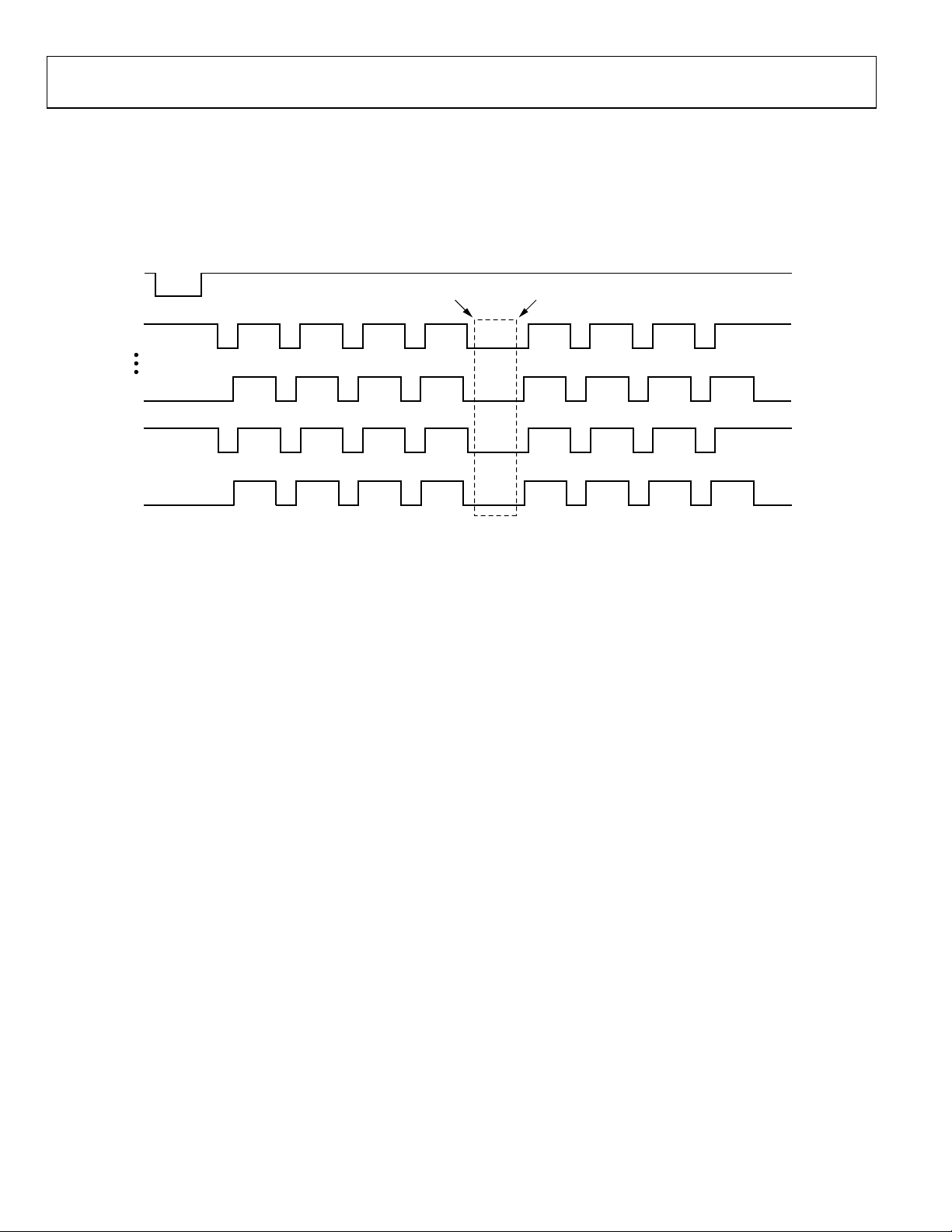
AD9920A
X
Hold Area Using the FREEZE/RESUME Registers
The FREEZE/RESUME registers can also be used to create a
hold area in which the V-outputs are temporarily held and later
continued, starting at the point where they were held. As shown
in Figure 53, the hold area function is different from the vertical
HD
FREEZE
XV1
XV8
XV9
V10
NOTES
1. WHEN HOL D = 1 FOR ANY V-SEQUENCE GROUP, THE FREEZE AND RESUME REGISTERS ARE USED TO SPECIFY THE HOL D ARE A.
2. IN THIS EXAMPLE, XV1 TO XV10 ARE ASSIGNED TO GROUP A. HOLD BIT FOR GROUP A = 1.
3. H-COUNTER F OR GROUP A (XV1 TO XV10) S TOPS DURING HOLD AREA.
Figure 53. Hold Area for Group A
masking function in that the V-outputs continue from where
they stopped rather than continuing from where they would
have been. The hold area temporarily stops the pixel counter
for the V-outputs, whereas vertical masking allows the counter
to continue in the masking area.
HOLD AREA
FOR GROUP A
RESUME
6878-052
Rev. B | Page 42 of 112

AD9920A
X
X
Special Pattern Insertion
Additional flexibility is available using the SPC_PAT_EN
register bits, which allow a Group B, Group C, or Group D
pattern to be inserted into a series of Group A repetitions. This
feature is useful when a different pattern is needed at the start,
middle, or end of a sequence.
Figure 54 shows an example of a sweep region using VPATA
with multiple repetitions where a single repetition of VPATB
has been added into the middle of the sequence. Figure 55
shows more detail on how to set the registers to achieve the
desired timing.
Note that VREPB is used to specify which repetition number
has the special pattern inserted instead of VPATA. VPATB
always has priority over VPATC or VPATD if more than one
SPC_PAT_EN bit is enabled (that is, SPC_PAT_EN, Bit 0 has
priority over SPC_PAT_EN, Bit 1 and Bit 2).
VD
HD
V1 TO XVx
LINE 0 LINE 1
REGION 0 REGION 2
SCP1 SCP2
LINE 24 LINE 25LINE 2
REGION 1: SWEEP REGION
PATTERN B INSERT E D DURI NG PATTERN A REPETITIONS
6878-053
Figure 54. Special Pattern Insertion Example
HD
REP 1 REP 2
V1
V-PATTERN A
REGISTER SETTINGS: DESCRIPTION:
SPC_PAT_EN[0] = 1 V-PATT E RN B IS USED AS SPECI AL PATTERN
VREPA = N TOTAL NUM BE R OF REPS USED FOR SEQUENCE ( N RE P S)
VREPB = 4 REP 4 USES V-PATTERN B INSTEAD OF V-PATTERN A
NOTES
1. VSTARTB MUST BE SET EQUAL TO VSTARTA.
V-PATTERN B V-PATTERN A
REP 5REP 4REP 3
Figure 55. Special Pattern Insertion Registers
REP N
06878-054
Rev. B | Page 43 of 112

AD9920A
Sequence Line Alternation
To support the timing requirements of some advanced CCDs
in a memory-efficient manner, the AD9920A can automatically
increment the sequence number at the end of a given line through
the use of the SEQ_ALT_INC register (V-Sequence Register 0x09,
Bit 20). It can also reset the sequence number to the sequence
defined in the field register through the SEQ_ALT_RST register
(V-Sequence Register 0x09, Bit 21). Combining these two registers
allows the user to create a loop of sequences for a given region.
See Figure 56 for an example of how to use these two functions
together. The example in Figure 56 uses the register settings
listed in Table 1 8.
With these settings, at Sequence Change Position 0 (SCP0),
the AD9920A steps into Sequence 2. Because the Sequence 2
SEQ_ALT_INC = 1 and the SEQ_ALT_RST = 0, at the end of
Table 18. Register Settings for the Example in Figure 56
Field Registers Sequence 2 Registers Sequence 3 Registers Sequence 4 Registers Sequence 6 Registers
SCP0 = 0, SEQ0 = 2 SEQ_ALT_INC = 1 SEQ_ALT_INC = 1 SEQ_ALT_INC = 0 SEQ_ALT_INC = 0
SCP1 = 6, SEQ1 = 6 SEQ_ALT_RST = 0 SEQ_ALT_RST = 0 SEQ_ALT_RST = 1 SEQ_ALT_RST = 0
that line the sequence number automatically increments to
Sequence 3. In the same way, at the end of that line, the
sequence number automatically increments to Sequence 4.
Because SEQ_ALT_INC = 0 and SEQ_ALT_RST = 1 for
Sequence 4, the AD9920A automatically resets the sequence
number to the sequence defined for that region in the field register,
which in this case is Sequence 2. The AD9920A continues to loop
in this fashion between Sequence 2, Sequence 3, and Sequence 4
until it reaches the next sequence change position.
It is important to note that the sequence number can increment
only at the end of a line and cannot be used to create more complex
patterns within one line. This is distinctly different from the special
vertical sequence alternation mode, which allows the user to
concatenate multiple sequences within one line (see the Special
Vertical Sequence Alternation (SVSA) Mode section).
VD
HD
ACTIVE
SEQUENCE #
SCP0
23423466
SCP1
Figure 56. Example Output Using SEQ_ALT_INC and SEQ_ALT_RST Functions
06878-055
Rev. B | Page 44 of 112

AD9920A
Complete Field: Combining V-Sequences
After the V-sequences are created, they are combined to create
different readout fields. A field consists of up to nine regions;
within each region, a different V-sequence can be selected.
Figure 57 shows how the sequence change positions (SCPs)
designate the line boundary for each region and how the SEQ
registers then select which V-sequence is used in each region.
Registers to control the VSG outputs are also included in the
field registers. Table 1 9 summarizes the registers used to create
the various fields.
The SEQ registers, one for each region, select which of the
V-sequences are active in each region. The MULT_SWEEP
registers, one for each region, are used to enable sweep mode
and/or multiplier mode in any region. The SCP registers create
the line boundaries for each region. The VDLEN register specifies
the total number of lines in the field. The HDLEN registers specify
the total number of pixels per line.
Table 19. Field Registers (CLPOB, PBLK Masking Shown in Table 11)
Register Length (Bits) Range Description
SEQ 5 0 to 31 V-sequence number Selected V-sequence for each region in the field.
MULT_SWEEP 2 0 to 3 Enable multiplier mode and/or sweep mode for each region.
SCP 13 0 to 8191 line number Sequence change position for each region.
VDLEN 13 0 to 8191 lines Total number of lines in each field.
HDLASTLEN 13 0 to 8191 pixels Length in pixels of the last HD line in each field.
VSGPATSEL 24 High/low
SGMASK 24 High/low, each VSG Set high to mask each individual VSG output.
SGACTLINE1 13 0 to 8191 line number Selects the line in the field where the VSG signals are active.
SGACTLINE2 13 0 to 8191 line number
0 = multiplier off, sweep off.
1 = multiplier off, sweep on.
2 = multiplier on, sweep off.
3 = multiplier on, sweep on.
VSGPATSEL selects which two V-pattern toggle positions are used by each
V-output. Each bit represents one V-output: Bit 0 = XV1 output, Bit 23 =
XV24 output.
0 = use TOG1 and TOG2.
1 = use TOG3 and TOG4.
Bit 0: XV1 mask.
Bit 23: XV24 mask.
Selects a second line in the field to repeat the VSG signals. If this register is
not used, set it equal to SGACTLINE1 or to the maximum value.
The HDLASTLEN register specifies the number of pixels in the
last line of the field.
The SGMASK register is used to enable or disable each individual
VSG output. There are two bits for each VSG output to enable
separate masking in SGACTLINE1 and SGACTLINE2.
Setting a masking bit high masks the output; setting it low
enables the output. The VSGPATSEL register assigns one of
the eight SG patterns to each VSG output. The individual SG
patterns are created separately using the SG pattern registers.
The SGACTLINE1 register specifies which line in the field
contains the VSG outputs. The optional SGACTLINE2 register
allows VSG pulses to be output on a different line. Separate
masking is not available for SGACTLINE1 and SGACTLINE2,
unless separate sequences are assigned to SGACTLINE1 and
SGACTLINE2. Note that to ensure proper SUBCK operation
when using both SGACTLINE1 and SGACTLINE2, SGACTLINE2
must be programmed to occur before SGACTLINE1.
Rev. B | Page 45 of 112

AD9920A
X
X
V1 TO XVx
SCP0
VD
HD
VSG
FIELD SETTINGS:
1. SEQUENCE CHANGE POSITIONS (S CP0 TO SCP8) DEFINE EACH OF THE NINE AVAILABLE REGI ONS IN THE F IELD.
2. SEQ0 TO SEQ8 SELECT THE DESIRED V-SEQUENCE FOR EACH REGION.
3. SGACTL INE1 REGIS TER SELECT S WHICH HD LINE IN THE FI E LD CONTAINS THE SENSOR G ATE PULSE(S ) .
SCP1 SCP2
REGION 0
SEQ0 SEQ1
REGION 1 REGION 2 REGION 3 REGION 4 REGION 8
SCP3
SEQ2
SGACTLINE1
Figure 57. Complete Field Divided into Regions
VD
HD
V1 TO XVx
LINE 0 LINE 1
REGION 0 REGION 2
SCP1 SCP2
Figure 58. Example of Sweep Region for High Speed Vertical Shift
Sweep Mode Operation
The AD9920A contains an additional mode of vertical timing
operation called sweep mode. This mode is used to generate a
large number of repetitive pulses that span across multiple HD
lines. An example of where this mode is needed is at the start of
the CCD readout operation. At the end of the image exposure
before the image is transferred by the sensor gate pulses, the
vertical interline CCD registers should be free of all charge. This
can be accomplished by quickly shifting out any charge using a
long series of pulses from the vertical outputs. Depending on
the vertical resolution of the CCD, up to 3000 clock cycles
might be needed to shift the charge out of each vertical CCD
line. This operation spans across multiple HD line lengths.
Normally, the AD9920A vertical timing must be contained
within one HD line length, but when sweep mode is enabled,
the HD boundaries are ignored until the region is finished. To
enable sweep mode within any region, program the appropriate
SWEEP register to high.
SCP4
SEQ3
REGION 1: SWEEP REGION
SEQ4
Figure 58 shows an example of the sweep mode operation. The
number of vertical pulses needed depends on the vertical resolution of the CCD. The toggle positions for the XV1 to XV24
signals are generated using the V-pattern registers (see Tabl e 14 ).
A single pulse is created using the polarity and toggle position
registers. The number of repetitions is then programmed to match
the number of vertical shifts required by the CCD. Repetitions
are programmed into the V-sequence registers using the VREP
registers (see Tab l e 15 ). This produces a pulse train of the appropriate length. Normally, the pulse train is truncated at the end
of the HD line length, but when sweep mode is enabled for this
region, the HD boundaries are ignored.
In Figure 58, the sweep region occupies 23 HD lines. After the
sweep mode region is complete, normal sequence operation
resumes in the next region. When using sweep mode, be sure to
set the region boundaries (using the sequence change positions)
to the appropriate lines to prevent the sweep operation from
overlapping with the next V-sequence.
SCP5
SCP8
SEQ8
LINE 24 LINE 25LINE 2
06878-056
06878-057
Rev. B | Page 46 of 112

AD9920A
X
A
Multiplier Mode
To generate very wide vertical timing pulses, a vertical region
can be configured into a multiplier region. This mode uses the
V-pattern registers in a slightly different manner. Multiplier
mode can be used to support unusual CCD timing requirements,
such as vertical pulses that are wider than the 13-bit V-pattern
toggle position counter. In general, the 13-bit toggle position
counter can be used with the sweep mode feature to support
very wide pulses; however, multiplier mode can be used to
generate even wider pulses.
The start polarity and toggle positions are still used in the same
manner as in the standard V-pattern group programming, but
VLEN is used differently. Instead of using the pixel counter
(HD counter) to specify the toggle position locations (VTOG1,
VTOG2, VTOG3, and VTOG4) of the V-pattern group, the
VLEN is multiplied by the VTOG position to allow very long
pulses to be generated.
Table 20. Multiplier Mode Register Parameters
Register Length (Bits) Range Description
MULT_SWEEPx 1 High/low High enables multiplier mode.
VPOL 1 High/low Starting polarity of XV1 to XV24 signals in each V-pattern group.
VTOG 13
0 to 8191 pixel
Toggle positions for XV1 to XV24 signals in each V-pattern group.
location
VLEN 13 0 to 8191 pixels Used as multiplier factor for toggle position counter.
VREP 13
0 to 8191 pixel
location
With VREP_MODE = 0, VREP_EVEN must be set to the same value as the highest VTOG
value. VREP_ODD and VREPA can be set to 0.
START POSITION OF VP
T GROUPIS STILL PROGRAMM E D IN THEV-SEQUENCE REG ISTERS
To calculate the exact toggle position, which is counted in pixels
after the start position, use the following equation:
Multiplier Mode Toggle Position = VTOG × VLEN
Because the VTOG register is multiplied by VLEN, the resolution of the toggle position placement is reduced. If VLEN = 4,
the toggle position precision is reduced to four-pixel increments
instead of to single-pixel increments. Table 2 0 summarizes how
the V-pattern group registers are used in multiplier mode operation. In multiplier mode, the VREP registers must always be
programmed to the same value as the highest toggle position.
Figure 59 illustrates this operation. The first toggle position is 2,
and the second toggle position is 9. In nonmultiplier mode, this
causes the V-sequence to toggle at Pixel 2 and then at Pixel 9
within a single HD line. However, in multiplier mode, toggle
positions are multiplied by the value of VLEN (in this case, 4);
therefore, the first toggle occurs at Pixel 8, and the second toggle
occurs at Pixel 36. Sweep mode is also enabled to allow the
toggle positions to cross the HD line boundaries.
HD
55
4
2
6878-058
VLEN
PIXEL
NUMBER
V1 TO XV24
3
1234123412341234123412341234123412341234
12345678910111213141516171819202122232425262728293031323334353637383940
4
1
MULTIPLIER MODE V-PATTERN GROUP PROPERTIES:
1
START POLARITY (STARTPOL = 0).
2
FIRST, S ECOND, AND THIRD TOGGLE POSITIONS (VTOG1 = 2, VTOG2 = 9).
3
LENGTH O F VPAT COUNTE R ( V LEN = 4); THI S IS THE MINIMUM RESOL UTION FO R T OGGLE P OSITIO N CHANGES.
4
TOGGLE POSITIONS OCCUR AT LOCATION E QUAL TO (V TOG × VL EN).
5
IF SWEE P REGION IS ENABLED, THE V - P ULSES MAY ALS O CROSS THE HD BO UNDARI E S , AS SHOWN ABO VE.
2
Figure 59. Example of Multiplier Region for Wide Vertical Pulse Timing
Rev. B | Page 47 of 112

AD9920A
VSG
Vertical Sensor Gate (Shift Gate) Patterns
In an interline CCD, the vertical sensor gate (VSG) pulses are
used to transfer the pixel charges from the light-sensitive image
area into light-shielded vertical registers. From the light-shielded
vertical registers, the image is clocked out line-by-line using the
vertical transfer pulses (XV signals) in conjunction with the high
speed horizontal clocks. The AD9920A has 24 vertical signals,
and each signal can be assigned as a VSG pulse instead of as an
XV pulse.
Tabl e 21 summarizes the VSG control registers, which are
mainly located in the field register space (see Ta ble 19). The
VSGSELECT register (Address 0x1C in the fixed address space)
determines which vertical outputs are assigned as VSG pulses.
When a signal is selected to be a VSG pulse, only the starting
polarity and two of the V-pattern toggle positions are used. The
VSGPATSEL register in the V-sequence registers is used to assign
either TOG1 and TOG2 or TOG3 and TOG4 to the VSG signal.
Table 21. VSG Control Registers (also see Field Registers in Table 19)
Register Length (Bits) Range Description
VSGSELECT
24 High/low
(Located in Fixed
Address Space, 0x1C)
Bit 0: XV1 selection (0 = XV pulse; 1 = VSG pulse).
Bit 1: XV2 selection.
Bit 23: XV24 selection.
VSGPATSEL 24 High/low
Bit 0: XV1 selection (0 = use TOG1, TOG2; 1 = use TOG3, TOG4).
Bit 1: XV2 selection.
Bit 23: XV24 selection.
SGMASK 24 High/low, each VSG Set high to mask each individual VSG output.
SGACTLINE1 13 0 to 8191 line number Selects the line in the field where the VSG signals are active.
SGACTLINE2 13 0 to 8191 line number
Note that only two of the four V-pattern toggle positions are
available when a vertical signal is selected to be a VSG pulse.
The SGACTLINE1 and SGACTLINE2 registers are used to
select which line in the field is the VSG line. The VSG active
line location is used to reference when the substrate clocking
(SUBCK) signal begins to operate in each field. For more information, see the Substrate Clock Operation (SUBCK) section.
Also located in the field registers, the SGMASK register selects
which individual VSG pulses are active in a given field. Therefore,
all SG patterns to be preprogrammed into the V-pattern registers
and the appropriate pulses for the different fields can be enabled
separately.
The AD9920A is an integrated AFETG and V-driver, so the
connections between the AFETG and V-driver are fixed, as
shown in Figure 65 and Figure 66. The VSGSELECT register
must be programmed to 0xFF8000.
Selection of VSG signals from XV signals. Set to 1 to make signal a VSG.
The recommended setting for this register is 0xFF8000.
When VSG signal is selected using the VSGSELECT register, VSGPATSEL
selects which V-pattern toggle positions are used. When this register is
set to 0, Toggle 1 and Toggle 2 are used. When this register is set to 1,
Toggle 3 and Toggle 4 are used.
Bit 0: XV1 mask.
Bit 23: XV24 mask.
Selects a second line in the field to repeat the VSG signals. If this register
is not used, set it equal in value to SGACTLINE1 or to the maximum value.
VD
4
HD
12
PATTERN
PROGRAMMABLE S E TTINGS FOR EACH PATT ERN:
1
START POLARITY OF PULSE (FROM VPOL IN SEQUENCE REGISTERS).
2
FIRST TOGGLE POSITION (FROM V-PATTERN REGISTERS).
3
SECOND TOGGLE POSITION (FROM V-PATTERN REGISTERS).
4
ACTIVE LINE FOR VSG PULSES WITHIN THE FIELD (FROM FIELD REGISTERS).
Figure 60. Vertical Sensor Gate Pulse Placement
Rev. B | Page 48 of 112
3
06878-059

AD9920A
Mode Registers
The mode registers are used to select the field timing of the
AD9920A. Typically, all of the field, V-sequence, and V-pattern
information is programmed into the AD9920A at startup. During
operation, the mode registers allow the user to select any combination of field timing to meet the requirements of the system.
The advantage of using the mode registers in conjunction with
preprogrammed timing is that it greatly reduces the system programming requirements during camera operation. Only a few
register writes are required when the camera operating mode is
changed; the vertical timing information does not need to be
changed with each camera mode change.
A basic still camera application can require six fields of vertical
timing—one for draft mode operation, one for autofocusing,
and four for still image readout. All of the register timing information for the six fields is loaded at startup. Then, during camera
operation, the mode registers select which field timing is active,
depending on how the camera is being used.
Tabl e 22 shows how the mode registers are used. The mode
register (Address 0x2A) specifies how many total fields are used.
Any value from 1 to 7 can be selected using these three bits.
The other two registers (Address 0x2B and Address 0x2C) are
used to select which of the programmed fields are used and in
which order. Up to seven fields can be used in a single write to
the mode register. The AD9920A starts with the field timing
specified by FIELD1, and on the next VD switches to the timing
specified by FIELD2, and so on. After completing the total
number of fields specified by the mode register, the AD9920A
repeats by starting at the first field. This continues until a new
write to the mode register occurs. Figure 61 shows example
mode register settings for different field configurations.
Note that only a write to Address 0x2C properly resets the field
counter. Therefore, when changing the values in any of the mode
registers, it is recommended that all three registers be updated
together in the same field (VD period).
Caution
The mode registers are SCK updated by default. If they are
configured as VD-updated registers by writing Address 0xB4 =
0x03FF and Address 0xB5 = 0xFC00, the new mode information is updated on the second VD falling edge after the write
occurs, rather than on the first VD falling edge. See Figure 63
for an example.
Table 22. Mode Registers
Address Name Length (Bits) Description
0x2A MODE 3 Total number of fields to cycle through. Set from 1 to 7.
0x2B FIELD1 5 Selected field (from FIELD registers in configurable memory) for the first field to cycle through.
FIELD2 5 Selected field (from FIELD registers in configurable memory) for the second field to cycle through.
FIELD3 5 Selected field (from FIELD registers in configurable memory) for the third field to cycle through.
FIELD4 5 Selected field (from FIELD registers in configurable memory) for the fourth field to cycle through.
FIELD5 5 Selected field (from FIELD registers in configurable memory) for the fifth field to cycle through.
0x2C FIELD6 5 Selected field (from FIELD registers in configurable memory) for the sixth field to cycle through.
FIELD7 5 Selected field (from FIELD registers in configurable memory) for the seventh field to cycle through.
Rev. B | Page 49 of 112

AD9920A
EXAMPLE 1:
TOTAL FIELDS = 3, FIRST FIELD = FIELD1, S E COND FIEL D = FIELD2, THIRD FIE LD = FIELD3
MODE SETTINGS:
0x2A = 0x03
0x2B = 0x820
0x2C = 0x00
FIELD1
EXAMPLE 2:
TOTAL FIELDS = 1, FIRST FIELD = FIELD3
MODE SETTINGS:
0x2A = 0x01
0x2B = 0x03
0x2C = 0x00
FIELD3
EXAMPLE 3:
TOTAL F IELDS = 4, FIRST FIELD = FIELD5, SE CO ND FIELD = FIELD1, THIRD FIELD = FIEL D4, FOURTH FIELD = F IELD2
MODE SETTINGS:
0x2A = 0x04
0x2B = 0x11025
0x2C = 0x00
FIELD5
FIELD2 FIELD3
FIELD1 FIELD4
FIELD2
6878-062
Figure 61. Using the Mode Registers to Select Field Timing
VD
MODE UPDATEMODE WRITE
REGISTER WRITE
MODE FIE LD NUMBER 4 (DRAFT) 4 (DRAFT) 0
EXAMPLE MO DE RE GISTER CHANGE :
REGIST E R WRITE A––WRITE TO MODE REG ISTERS 0x2A, 0x2B, 0x2C TO SPECIFY
CHANGE FROM DRAFT MODE (FIELD4) TO STI LL MODE ( FIELD1/ 2/3).
ALSO WRITE TO VGA GAIN OR ANY NEW REGISTER VALUES NEEDED
FOR STI LL FRAME OPERATION, S UCH AS NE W FIELD INFORMATION.
A
(STILL FIRST FIELD)
1
(STILL SECOND FIELD)
2
6878-060
Figure 62. Update of Mode Register, SCK Updated (Default Setting)
VD
MODE WRITE
REGISTER WRITE
MODE FIE LD NUMBER 4 (DRAFT) 4 (DRAFT)
AB
EXAMPLE MO DE RE GISTER CHANGE :
REGIST E R WRITE A––WRITE TO MODE REG ISTERS 0x2A, 0x2B, 0x2C TO SPECIFY
CHANGE FROM DRAFT MODE (FIELD4) TO STI LL MODE ( FIELD1/ 2/3).
REGISTER WRITE B––WRITE TO VGA GAIN OR ANY NEW REGISTER VALUES NEEDED
FOR STI LL FRAME OPERATION, S UCH AS NE W FIELD INFORMATION.
NOTES
1. NEW MODE INFORMATION IS UPDATED AT SECOND V D F ALLING E DGE AFTER
SERIAL WRITE A.
MODE UPDATE
0
(STILL FIRST FIELD)1 (STILL SECOND FIELD)
2
06878-061
Figure 63. Update of Mode Register, VD Updated
Rev. B | Page 50 of 112

AD9920A
VERTICAL TIMING EXAMPLE
To better understand how the AD9920A vertical timing generation is used, consider the example CCD timing chart in Figure 64.
This example illustrates a CCD using a general three-field readout technique. As shown in Figure 64, each readout field must be
divided into separate regions to perform each step of the readout.
The sequence change positions (SCPs) determine the line boundaries for each region, and the SEQ registers assign a particular
V-sequence to each region. The V-sequences contain the specific
timing information required in each region: V1 to V6 pulses
(using V-pattern groups), HBLK/CLPOB timing, and VSG
patterns for the SG active lines.
This timing example requires four regions for each of the three
fields, labeled Region 0, Region 1, Region 2, and Region 3. Because
the AD9920A allows many individual fields to be programmed,
FIELD1, FIELD2, and FIELD3 can be used to meet the requirements of this timing example. The four regions for each field are
very similar in this example, but the individual registers for each
field allow flexibility to accommodate other timing charts.
Region 0 is a high speed, vertical shift region. Sweep mode can be
used to generate this timing operation with the desired number
of high speed vertical pulses needed to clear any charge from
the CCD vertical registers.
Region 1 consists of only two lines and uses standard single-line
vertical shift timing. The timing of this region area is the same
as the timing in Region 3.
Region 2 is the sensor gate line in which the VSG pulses transfer
the image into the vertical CCD registers. This region may require
the use of the second V-pattern group for the SG active line.
Region 3 also uses the standard single-line vertical shift timing,
the same timing as Region 1. Four regions are required in each
of the three fields.
The timing for Region 1 and Region 3 is essentially the same,
reducing the complexity of the register programming. Other
registers must be used during the actual readout operation.
These include the mode registers, shutter control registers
(PRIMARY_ACTION, SUBCK, and GPO for MSHUT and
VSUB control), and AFE gain registers.
Important Note Regarding Signal Polarities
When programming the AD9920A to generate the V1 to V24
and SUBCK signals, the external V-driver circuit usually inverts
these signals. Carefully check the timing signals that are required
at the input and output of the V-driver circuit being used, and
adjust the polarities of the AD9920A outputs accordingly.
Rev. B | Page 51 of 112

AD9920A
OPEN
N
N – 3
21
18
15
12
9
6
3
REGION 1 REGION 2
REGION 0 REGION 3
THIRD FIE LD READOUT
N – 1
N – 4
20
17
14
11
8
5
2
SECOND FIELD READOUT
) FIRST FIELD READOUT
t
EXPOSURE (
EXP
FIELD 1 FIELD 2
REGION 1 REGION 2
REGION 0 REGION 3
N – 2
N – 5
16
13
10
7
4
1
FIELD 0
REGION 1 REGION 2
REGION 0 REGION 3
CLOSED
OPEN
VD
HD
V1
V3
V2
V4
V6
SUBCK
MSHUT
VSUB
CCD
V5
OUT
06878-063
Figure 64. CCD Timing Example—Dividing Each Field into Regions
Rev. B | Page 52 of 112

AD9920A
INTERNAL VERTICAL DRIVER CONNECTIONS (18-CHANNEL MODE)
AD9920A
INTERNAL
TIMING
GENERATOR
XV16 (XSG1)
XV1
XV17 (XSG2)
XV18 (XSG3)
XV2
XV19 (XSG4)
XV20 (XSG5)
XV3
XV21 (XSG6)
XV4
XV22 (XSG7)
XV5
XV23 (XSG8)
XV6
XV24 (XSG9)
XV7
+3V
V-DRIVER
VH,VL
G9
G6
G5
J9
D10
V1A
V1B
V2A
E9
V2B
V3A
F6
V3B
F5
V4
E5
V5
V6
F9
V7
3-LEVEL OUTPUTS
XV8
XV9
XV10
XV11
XV12
XV13
XV14
XV15
XSUBCK
J6
LEGEN
F7
V8
D9
V9
C4
V10
C5
V11
B5
V12
E6
V13
E7
V14
C8
V15
J8
V16
G7
SUBCK
K11
XSUBCNT (LOG I C I NPUT)
Figure 65. Internal AFETG to V-Driver Connections, Legacy Mode (18-Channel Mode)
2-LEVEL OUTPUTS
2-LEVEL OUTPUT,
REDUCED DRIVE
06878-064
Rev. B | Page 53 of 112

AD9920A
INTERNAL VERTICAL DRIVER CONNECTIONS (19-CHANNEL MODE)
AD9920A
INTERNAL
TIMING
GENERATOR
XV16 (XSG1)
XV1
XV17 (XSG2)
XV18 (XSG3)
XV2
XV19 (XSG4)
XV3
XV20 (XSG5)
XV23
XV21 (XSG6)
XV4
XV22 (XSG7)
XV5
GPO5 (XSG8)
XV6
GPO6 (XSG9)
XV7
+3V
V-DRIVER
VH,VL
G9
G6
G5
J9
D10
V1A
V1B
V2A
E9
V2B
V3A
F6
V3B
F5
V4
E5
V5
V6
F9
V7
3-LEVEL OUTPUTS
XV8
XV9
XV10
XV11
XV12
XV13
XV14
XV15
XV24
XSUBCK
J6
LEGEN
+3V
F7
V8
D9
V9
C4
V10
C5
V11
B5
V12
E6
V13
E7
V14
C8
V15
J8
V16
G7
SUBCK
K11
XSUBCNT (LOG I C I NP UT )
2-LEVEL OUTPUTS
2-LEVEL OUTPUT,
REDUCED DRIVE
06878-065
Figure 66. Internal AFETG to V-Driver Connections (19-Channel Mode)
Rev. B | Page 54 of 112

AD9920A
OUTPUT POLARITY OF VERTICAL TRANSFER CLOCKS AND SUBSTRATE CLOCK
Table 23. V1A Output Polarity
Vertical Driver Input
LEGEN
XV1 XV16 (XSG1) V1A Output
X L L VH
X L H VM
X H L VL
X H H VL
Table 24. V1B Output Polarity
Vertical Driver Input
LEGEN
XV1 XV17 (XSG2) V1B Output
X L L VH
X L H VM
X H L VL
X H H VL
Table 25. V2A Output Polarity
Vertical Driver Input
LEGEN
XV2 XV18 (XSG3) V2A Output
X L L VH
X L H VM
X H L VL
X H H VL
Table 26. V2B Output Polarity
Vertical Driver Input
LEGEN
XV2 XV19 (XSG4) V2B Output
X L L VH
X L H VM
X H L VL
X H H VL
Table 27. V3A Output Polarity
Vertical Driver Input
LEGEN
XV3 XV20 (XSG5) V3A Output
X L L VH
X L H VM
X H L VL
X H H VL
Table 28. V3B Output Polarity
Vertical Driver Input
XV21
LEGEN
XV3 XV23
(XSG6)
V3B Output
L L X L VH
L L X H VM
L H X L VL
L H X H VL
H X L L VH
H X L H VM
H X H L VL
H X H H VL
Rev. B | Page 55 of 112
Table 29. V4 Output Polarity
Vertical Driver Input
LEGEN
XV4 XV22 (XSG7) V4 Output
X L L VH
X L H VM
X H L VL
X H H VL
Table 30. V5 Output Polarity
Vertical Driver Input
LEGEN
XV5
(XSG8)
XV23
GPO5
(XSG8) V5 Output
L L L X VH
L L H X VM
L H L X VL
L H H X VL
H L X L VH
H L X H VM
H H X L VL
H H X H VL
Table 31. V6 Output Polarity
Vertical Driver Input
LEGEN
XV6
(XSG9)
XV24
GPO6
(XSG9) V6 Output
L L L X VH
L L H X VM
L H L X VL
L H H X VL
H L X L VH
H L X H VM
H H X L VL
H H X H VL
Table 32. V7 Output Polarity
Vertical Driver Input
LEGEN
XV7 V7 Output
X L VM
X H VL
Table 33. V8 Output Polarity
Vertical Driver Input
LEGEN
XV8
V8 Output
X L VM
X H VL
Table 34. V9 Output Polarity
Vertical Driver Input
LEGEN
XV9
V9 Output
X L VM
X H VL

AD9920A
Table 35. V10 Output Polarity
Vertical Driver Input
LEGEN
XV10
V10 Output
X L VM
X H VL
Table 40. V15 Output Polarity
Vertical Driver Input
LEGEN
XV15
V15 Output
X L VM
X H VL
Table 36. V11 Output Polarity
Vertical Driver Input
LEGEN
XV11
V11 Output
X L VM
X H VL
Table 37. V12 Output Polarity
Vertical Driver Input
LEGEN
XV12
V12 Output
X L VM
X H VL
Table 38. V13 Output Polarity
Vertical Driver Input
LEGEN
XV13
V13 Output
X L VM
X H VL
Table 39. V14 Output Polarity
Vertical Driver Input
LEGEN
XV14
V14 Output
X L VM
X H VL
Table 41. V16 Output Polarity
Vertical Driver Input
LEGEN
XV24
V16 Output
L X VL
H L VM
H H VL
Table 42. SUBCK Output Polarity
Vertical Driver Input
LEGEN
XSUBCK XSUBCNT
SUBCK Output
X L L VH
X L H VH
X H L VMM
X H H VLL
Rev. B | Page 56 of 112

AD9920A
XV1
XV16 (XSG1)
VH
V1A
VM
XV1
XV17 (XSG2)
V1B
VM
XV2
XV18 (XSG3)
V2A
VM
VL
VH
VL
VH
Figure 67. XV1, XV16, and V1A Output Polarities
Figure 68. XV1, XV17, and V1B Output Polarities
06878-066
06878-067
XV2
XV19 (XSG4)
V2B
VM
VL
VH
VL
Figure 69. XV2, XV18, and V2A Output Polarities
Figure 70. XV2, XV19, and V2B Output Polarities
Rev. B | Page 57 of 112
06878-068
06878-069

AD9920A
XV3
XV20 (XSG5)
VH
V3A
VM
XV3
XV21 (XSG6)
V3B
VM
XV23
XV21 (XSG6)
V3B
VM
VL
VH
VL
VH
Figure 71. XV3, XV20, and V3A Output Polarities
Figure 72. XV3, XV21, and V3B Output Polarities (
LEGEN
= Low)
06878-070
06878-071
XV4
XV22 (XSG7)
V4
VM
VL
VH
VL
Figure 73. XV23, XV21, and V3B Output Polarities (
Figure 74. XV4, XV22, and V4 Output Polarities
Rev. B | Page 58 of 112
LEGEN
= High)
06878-072
06878-073

AD9920A
G
X
XV5
XV23 (XSG8)
VH
V5
VM
GPO5 (XSG8)
V5
PO6 (XSG9)
V6
V7, XV8, XV9, XV10,
XV11, XV12, XV 13,
VL
XV5
VH
VM
VL
XV6
VH
VM
VL
XV14, XV15
Figure 75. XV5, XV23, and V5 Output Polarities (
Figure 76. XV5, GPO5, and V5 Output Polarities (
Figure 77. XV6, GPO6, and V6 Output Polarities (
LEGEN
LEGEN
LEGEN
= Low)
= High)
= High)
06878-074
06878-075
06878-077
V7, V8, V 9, V10, V11,
V12, V13, V 14, V15
VM
VL
06878-078
Figure 78. Two-Level V-Driver Output Polarities
LEGEN
XV24
VM
V16
VL
Figure 79. XV24 and V16 Output Polarities
Rev. B | Page 59 of 112
06878-079

AD9920A
XSUBCNT
XSUBCK
VH
SUBCK
VMM
VLL
Figure 80. XSUBCNT, XSUBCK, and SUBCK Output Polarities
V-DRIVER SLEW RATE CONTROL SUBSTRATE CLOCK OPERATION (SUBCK)
The AD9920A allows the user to moderate the slew rates of the
V-driver outputs when transitioning to VM and VL (this feature
does not affect transitions to VH). This feature minimizes coupling from V-driver activity that occurs while the AD9920A is
clocking valid image pixel data out of the CCD.
There are both coarse and fine mechanisms for controlling the
slew rate of the V1A to V13 outputs. If SRSW = VDD and
SRCTL = VDD, the V1A to V13 switches have roughly 10%
of their normal drive strength (that is, when SRSW = VSS).
If SRSW = VDD and SRCTL < VDD, the voltage applied to
SRCTL controls the slew rate for V1A to V13 transitions from
VM to VL and from VL to VM. For values from 800 mV to
VDD, V1A to V13 transition at a fraction of their maximum
slew rate that is roughly proportional to the voltage applied to
SRCTL. (It is not recommended that voltages less than 800 mV
be applied to SRCTL.)
The user must tune this voltage for the specific system to
determine the optimal setting that ensures maximum charge
transfer efficiency and minimizes any coupling from V-driver
activity into the image. V14, V15, and V16 are permanently
weak compared with V1A to V13 and are not affected by the
slew rate control function. Note that the slew rate control
feature is intended only for use with CCDs that require V-driver
activity outside the normal horizontal clock blanking region.
SHUTTER TIMING CONTROL
The AD9920A supports the generation of electronic shuttering
(SUBCK) and also features flexible general-purpose outputs
(GPOs) to control mechanical shuttering, CCD substrate bias
switching, and strobe circuitry. In the following sections, the
terms sense gate (SG) and vertical sense gate (VSG) are used
interchangeably.
The CCD image exposure time is controlled by the substrate
clock signal (SUBCK), which pulses the CCD substrate to clear
out accumulated charge. The AD9920A supports three types of
electronic shuttering: normal, high precision, and low speed.
Along with the SUBCK pulse placement, the AD9920A can
accommodate different readout configurations to further
suppress the SUBCK pulses during multiple field readouts.
The SUBCK signal is a programmable string of pulses, each
occupying a line following the primary sense gate active line,
SGACTLINE1 (see Tabl e 43 ). The SUBCK signal has programmable pulse width, line placement, and number of pulses to
accurately control the exposure time.
SUBCK Normal Operation
By default, the AD9920A operates in the normal SUBCK
configuration, in which the SUBCK signal is pulsing in every
VD field (see Figure 81). The SUBCK pulse occurs once per
line, and the total number of repetitions within the field
determines the length of the exposure time. The SUBCK
pulse polarity and toggle positions within a line are programmable using the SUBCK_POL and SUBCK_TOG1 registers
(see Tabl e 43 ). The number of SUBCK pulses per field is
programmed in the SUBCKNUM register (Address 0x75).
As shown in Figure 81, the SUBCK pulses always begin in the line
following the SG active line, which is specified in the SGACTLINE
registers for each field. The SUBCK_POL, SUBCK_TOG1,
SUBCK_TOG2, SUBCKNUM, and SUBCKSUPPRESS registers
are updated at the start of the line after the sensor gate line, as
described in the Updating New Register Values section.
06878-080
Rev. B | Page 60 of 112

AD9920A
SUBCK High Precision Operation
High precision shuttering is used in the same manner as normal
shuttering, but it uses an additional register to control the last
SUBCK pulse. In this mode, the SUBCK still pulses once per line,
but the last SUBCK in the field has an additional SUBCK pulse,
whose location is determined by the SUBCKHP_TOG registers,
as shown in Figure 82. Finer resolution of the exposure time is
possible using this mode. Leaving the SUBCKHP_TOG registers
set to their maximum value (0xFFFFFF) disables the last SUBCK
pulse (default setting).
SUBCK Low Speed Operation
Normal and high precision shutter operations are used when
the exposure time is less than one field. For exposure times greater
than one field, the low speed (LS) shutter features can be used.
The AD9920A includes a field counter (primary field counter)
to regulate long exposure times. The primary field counter
(Address 0x70) must be activated to serve as the trigger for the
LS operation. The durations of the LS exposure and read are
specified by the SGMASK_NUM and SUBCKMASK_NUM
registers (Address 0x74), respectively. As shown in Figure 83,
this mode suppresses the SUBCK and VSG outputs for up to
8192 fields (VD periods).
To activate an LS shutter operation, trigger the start of the
exposure by writing to the PRIMARY_ACTION register bits
according to the desired effect (see Tabl e 59 ). When the primary
counter is activated, the next VD period becomes the first active
period of the exposure for which the VSG and SUBCK masks
are applied.
Optionally, if the SUBCKMASK_SKIP1 register is enabled,
the AD9920A ignores the first VSG and SUBCK masks in the
subsequent fields. This is generally desired so that the exposure
time begins in the field after the exposure operation is initiated.
Figure 83 shows operation with SUBCKMASK_SKIP1 = 1. The
same functionality can also be achieved using the PRIMARY_
DELAY register along with the PRIMARY_ACTION register.
If the PRIMARY_ACTION register is used while the
SUBCKMASK_NUM and SGMASK_NUM registers are set to
0, the behavior of the SUBCK and VSG signals is not different
from the normal shutter or high precision shutter operations.
Therefore, the primary field counter can be used for other tasks
(described in the General-Purpose Outputs (GPOs) section)
without disrupting normal activity. In addition, a secondary
field counter is available that has no effect on the SUBCK and
VSG signals. These counters are described in detail in the Field
Counters section.
SUBCKSUPPRESS Register
By default, the SUBCK pulses begin in the line following
SGACTLINE1. For applications where the SUBCK pulse should
be suppressed for one or more lines following the VSG line, the
SUBCKSUPPRESS register can be programmed. This register
setting delays the start of the SUBCK pulses until the specified
number of lines following SGACTLINE1.
Read After Exposure
To read the CCD data after exposure, the SG should resume
normal activity while the SUBCK remains null. By default, the
AD9920A generates the VSG pulses in every field. When only
a single exposure and a single frame read are desired, as in the
case of preview mode, the VSG and SUBCK pulses can operate
in every field.
Other applications require that a greater number of frames be
read, in which case SUBCK must be masked until the readout is
finished. The SUBCKMASK_NUM register specifies the total
number of fields (exposure and read) to mask SUBCK. A two-field
CCD frame read mode typically requires two additional fields of
SUBCK masking (SUBCKMASK_NUM = 2). A three-field,
6-phase CCD requires three additional fields of SUBCK masking after the read begins (SUBCKMASK_NUM = 3).
Note that the SUBCKMASK_SKIP1 register setting allows
SUBCK pulses at the beginning of the field of exposure.
Table 43. SUBCK and Exposure/Read Register Parameters
Register Length (Bits) Range Description
SGMASK_NUM 13 0 to 8191 number of fields Exposure duration (number of fields to suppress VSG) for LS operation.
SUBCKMASK_NUM 13 0 to 8191 number of fields Exposure plus readout duration (number of fields to suppress SUBCK) for LS.
SUBCKMASK_SKIP1 1 On/off Suppress SG/SUBCK masks for one field (default = 0). Typically set to 1.
SUBCKSUPPRESS 13 0 to 8191 lines Number of lines to suppress the start of SUBCK pulses after SGACTLINE1.
SUBCKNUM 13 1 to 8191 number of pulses Total number of SUBCK pulses per field, at one pulse per line.
SG_SUPPRESS 1 On/off Suppress the SG and allow SUBCK to finish at SUBCKNUM.
SUBCK_TOG1 14 0 to 16383 pixel locations SUBCK Toggle Position 1.
SUBCK_TOG2 14 0 to 16383 pixel locations SUBCK Toggle Position 2.
SUBCK_POL 1 Low/high SUBCK start polarity.
SUBCKHP_TOG1 14 0 to 16383 pixel locations High precision SUBCK Toggle Position 1. Selectable as SG or VD updated.
SUBCKHP_TOG2 14 0 to 16383 pixel locations High precision SUBCK Toggle Position 2. Selectable as SG or VD updated.
Rev. B | Page 61 of 112

AD9920A
S
R
VD
HD
VSG
SUBCK
SUBCK PROGRAMMABLE SETTINGS:
1. PULSE POLARITY USING THE SUBCK_POL REGISTER.
2. NUMBER OF P ULSES WI T HIN THE FI E LD USING T HE SUBCKNUM REGIST E R ( S UBCKNUM = 3 IN THIS E X AM P LE).
3. PIXEL LOCATIO N OF PULSE W ITHIN THE LINE AND PULSE WIDTH PROGRAMMED USING T HE SUBCK_TOG1 T OGGLE P OSITI ON REGIST E R.
t
EXP
t
EXP
06878-081
Figure 81. Normal SUBCK Operation
VD
HD
VSG
UBCK
NOTES
1. SECOND SUBCK PULSE IS ADDED I N THE LAST S UBCK LINE.
2. LOCATION OF SECOND PULS E IS FULLY PROGRAMMABLE USING THE S UBCKHP TOGGLE POSITION REGISTERS.
t
EXP
t
EXP
6878-082
Figure 82. High Precision SUBCK Operation
TRIGGE
EXPOSURE
(0x70)
VD
VSG
t
EXP
SUBCK
NOTES
1. SUBCK CAN BE SUPPRESSE D FOR MULTIPLE FIELDS BY PRO GRAMMING T HE E XPOSURE REGI STER TO BE GREATER THAN 0.
2. THIS EXAMPLE USES EX POSURE = 1.
3. TRIGGER REGISTER MUST ALSO BE USED TO START THE LOW SPEED EXPOSURE.
4. VD/HD OUT PUTS CAN ALSO BE S UP P RES SED USING THE V DHD_MAS K RE GISTER = 1.
06878-083
Figure 83. Low Speed SUBCK Operation (SUBCKMASK_SKIP1 = 1)
Rev. B | Page 62 of 112

AD9920A
FIELD COUNTERS
The AD9920A contains three field counters (primary, secondary,
and mode). When these counters are active, they increment with
each VD cycle. The mode counter is the field counter used with
the mode register to control the vertical timing signals (see the
Mode Registers section).
The primary and secondary counters are more flexible and are
generally used for shuttering signal applications. Both the primary
and secondary counters have several modes of operation that
are selected by Address 0x70. These modes are as follows:
• Normal (single count)
• RapidShot (repeating count)
• ShotTimer (delayed count)
Table 44. Primary/Secondary Field Counter Registers (Address 0x70, Address 0x71, and Address 0x72)
Register Length (Bits) Description
PRIMARY_ACTION 3
SECOND_ACTION 3
2 = RapidShot. After reaching the maximum counter value, the counter wraps and repeats until reset.
6 = manual readout. Primary counter switches to readout (VSG pulses becomes active).
7 = force to idle.
PRIMARY_MAX 13 Primary counter maximum value.
SECOND_MAX 12 Secondary counter maximum value.
VDHD_MASK 3 Mask VD/HD during counter operation.
PRIMARY_DELAY 13
PRIMARY_SKIP 1 When using ShotTimer with RapidShot, use the primary delay value only before the first count (exposure).
SECOND_DELAY 13
SECOND_SKIP 1 When using ShotTimer with RapidShot, use the secondary delay value only before the first count.
0 = idle, no counter action. GPO signals can still be controlled using polarity or by setting the
appropriate GP_PROTOCOL register to 1.
1 = activate counter. Single cycle of counter from 1 to counter maximum value and then return to
idle state.
3 = ShotTimer. Active single cycle of counter after added delay of n fields (use the corresponding
DELAY register).
4 = ShotTimer with RapidShot. Same as RapidShot (SECOND_ACTION register = 2) but with an added
delay of n fields between each repetition.
5 = manual exposure. Primary counter stays in exposure until manual readout or reset to idle.
This mode keeps the SUBCK and VSG pulses masked indefinitely.
ShotTimer. Number of fields to delay before the next primary count (exposure) starts. If using
ShotTimer with RapidShot, the delay value is used between each repetition.
ShotTimer. Number of fields to delay before the next secondary count starts. If using ShotTimer with
RapidShot, the delay value is used between each repetition.
• ShotTimer with RapidShot
• Manual exposure
• Manual readout
• Force to idle
The primary counter regulates the expose and read actions
by regulating the SUBCK and VSG signals. In addition, if the
RapidShot feature is used with the primary counter, the SUBCK
and VSG masking automatically repeats as necessary for multiple
expose/read cycles. The secondary counter has no effect on the
SUBCK or VSG signal. Both counters can be used to regulate
the general-purpose signals described in the General-Purpose
Outputs (GPOs) section.
Rev. B | Page 63 of 112

AD9920A
GENERAL-PURPOSE OUTPUTS (GPOs)
The AD9920A provides programmable outputs to control a
mechanical shutter, the strobe/flash, the CCD bias select signal,
or any other external component with general-purpose (GP)
signals. Eight GP signals, with up to four toggles each, are
available to be programmed and assigned to special GPO pins.
These pins are bidirectional and allow visibility (as an output)
and external control (as an input) of HBLK, PBLK, CLPOB, and
OUT_CONTROL. The GPO registers are described in Ta bl e 45 .
Note that GPO5 and GPO6 are used to control the SG signals
for the V5 and V6 outputs of the AD9920A. See the SG Control
Using GPO section for more information.
GP Toggles
When configured as an output, each GPO output can deliver a
signal that is the result of programmable toggle positions. The
GP signals are independent and can be linked to a specific VD
period or to a range of VD periods via the primary or secondary
field counters through the GP protocol register (Address 0x73).
As a result of their associations with the field counters, the GP
toggles inherit the characteristics of the field counters, such as
RapidShot and ShotTimer.
To program the GP toggles, complete the following steps:
1. Program the toggle positions (Address 0x7C to
Address 0xAB).
2. Program the GP protocol (Address 0x73).
3. Program the counter parameters (Address 0x71 to
Address 0x72).
4. Activate the counter (Address 0x70).
For Protocol 1 (no counter association), skip Step 3 and Step 4.
With these four steps, the GP signals can be programmed to
accomplish many common tasks. Careful protocol selection and
application of the field counters yields efficient results to allow
the GP signals smooth integration with concurrent operations.
Note that the SUBCK and VSG masks are linked to the primary
counter; however, if their parameters are 0, the GPO can use the
primary counter without expose/read activity.
The secondary counter is independent and can be used simultaneously with the primary counter. Some applications may
require the use of both primary and secondary field counters
with different GPO protocols, start times, and durations. Such
operations are easily handled by the AD9920A.
Several simple examples of GPO applications using only one
GPO and one field counter follow. These examples can be used
as building blocks for more complex GPO activity. In addition,
specific GPO signals can be passed through a four-input lookup
table (LUT) to realize combinational logic between them. For
example, GP1 and GP2 can be sent through an XOR lookup
table, and the result can be delivered on GP1, GP2, or both. In
addition, GP1 or GP2 can deliver its original toggles.
Table 45. GPO Registers
Register Length (Bits) Range Description
GP1_PROTOCOL 3 0 to 7 0 = idle
GP2_PROTOCOL 3 0 to 7 1 = no counter association; use MANUAL_TRIG bits to enable each GP signal.
GP3_PROTOCOL 3 0 to 7 2 = test only.
GP4_PROTOCOL 3 0 to 7 3 = test only.
GP5_PROTOCOL 3 0 to 7 4 = link to mode counter (from vertical timing generation).
GP6_PROTOCOL 3 0 to 7 5 = link to primary counter (also allows GP signals to repeat with RapidShot).
GP7_PROTOCOL 3 0 to 7 6 = link to secondary counter (also allows GP signals to repeat with RapidShot).
GP8_PROTOCOL 3 0 to 7 7 = keep on.
MANUAL_TRIG 8 On/off Manual trigger for each GP signal. For use with Protocol 1.
GP[1:8]_POL 8 Low/high Starting polarity for GP signals. Only updated when GPx_PROTOCOL = 0.
SEL_GP[1:8] 8 On/off
GPO4: XSUBCK.
GPO5: XV21.
GPO6: XV22.
GPO7: XV23.
GPO8: XV24.
GPO_OUTPUT_EN 8 On/off
GPx_USE_LUT 8 On/off Send GP signals through a programmable lookup table (LUT).
LUT_FOR_GP12 4 Logic setting Desired logic to be realized on GPO1 combined with GPO2.
LUT_FOR_GP34 4 Logic setting Desired logic to be realized on GPO3 combined with GPO4.
LUT_FOR_GP56 4 Logic setting Desired logic to be realized on GPO5 combined with GPO6.
1 = select GP toggles visible at GPO1 to GPO4, GPO7, and GPO8 when output is
enabled (default).
0 = select vertical signals visible at GPO4 to GPO8 when output is enabled.
1 = enable GPO1 to GPO4, GPO7, and GPO8 outputs (one bit per output).
0 = disable GPO1 to GPO4, GPO7, and GPO8 outputs; pins are high-Z (default).
Rev. B | Page 64 of 112

AD9920A
Register Length (Bits) Range Description
LUT_FOR_GP78 4 Logic setting
0x06 = GPy XOR GPx (see Figure 89).
0x07 = GPy NAND GPx.
0x08 = GPy AND GPx.
0x0E = GPy OR GPx.
GPx_TOGx_FD 13 0 to 8191 fields Field of activity, relative to primary and secondary counter for corresponding toggle.
GPx_TOGx_LN 13 0 to 8191 lines Line of activity for corresponding toggle.
GPx_TOGx_PX 13 0 to 8191 pixels Pixel of activity for corresponding toggle.
GPO_INT_EN 1 On/off
GPO1 = internal clock.
GPO2 = CLPOB.
GPO3 = delayed sample clock.
Desired logic to be realized on GPO7 combined with GPO8.
Example logic settings for LUT_FOR_GPxy:
When set to 1, internal signals are viewable on GPO1 to GPO3. Also, set the
SEL_GPx bit low to output internal signals.
Rev. B | Page 65 of 112

AD9920A
Single-Field Toggles
Single-field toggles occur in the next field only. There can be up to
four toggles in the field. The mode is set with GP_PROTOCOL
equal to 1, and the toggles are triggered in the next field by
writing to the MANUAL_TRIG register (Register 0x70, Bits[13:6]).
In this mode, the field toggle settings must be set to a value of 1.
Two consecutive fields do not have activity. If toggles are required
to repeat in the next field, the MANUAL_TRIG register can be
written to in consecutive fields.
Preparation
The GP toggle positions can be programmed any time prior to
use. For example,
0x7C ← 0x000A001
0x7D ← 0x0002000
0x7E ← 0x000000F
0x7F ← 0x00C4002
0x80 ← 0x0004000
0x81 ← 0x00000B3
Details
A) Field 0: 0x70 ← 0x0000040
0x73 ← 0x0000001
B) Field 1: 0x73 ← 0x0000000
VD
REGISTER WRITE
GP1_PROTOCOL 0 1 0
GPO1
NOTES
1. THE FIELD TOGGLE PO SI T I O N MUST BE SET TO 1 WHEN
GP PROTOCOL IS 1.
CAUTION! THE GP_PRO TOCOL MUS T BE RESET BEFORE
USING AGAIN.
Figure 84. Single-Field Toggles Using GP_PROTOCOL = 1
AB
1
06878-084
Scheduled Toggles
Scheduled toggles are programmed to occur during upcoming
fields. For example, there can be one toggle in Field 1, two
toggles in Field 3, and a last toggle in Field 4. The mode is set
with GP_PROTOCOL = 5 or GP_PROTOCOL = 6. Mode 5
tells the GPO to obey the primary field counter, and Mode 6
tells the GPO to obey the secondary field counter.
Note that for GP_PROTOCOL = 5 or GP_PROTOCOL = 6, at
least one toggle must be programmed in Field 1 for the AD9920A
to output the proper pattern on the GPO pins. If no toggle is
programmed in Field 1, all subsequent toggle positions are
ignored when GP_PROTOCOL = 5 or GP_PROTOCOL = 6.
This restriction applies only to GP_PROTOCOL = 5 or
GP_PROTOCOL = 6.
Preparation
The GP toggle positions can be programmed any time prior to
use. For example,
0x7C ← 0x00C4001
0x7D ← 0x0004000
0x7E ← 0x00000B3
Details
A) Field 0: 0x70 ← 0x0000008
0x73 ← 0x0000006
VD 1 2
REGISTER WRITE
GP1_PROTOCOL
SECONDARY
COUNT
GPO1
Figure 85. Scheduled Toggles Using GP_PROTOCOL = 6
CAUTION! THE PRIMARY COUNTER REGULATES T HE SUBCK
AND VSG ACTIVITY. LINK A GPO TO THE PRIMARY COUNTER
ONLY IF S UBCK AND VS G ACTIVITY WILL OCCUR DURING
EXPOSURE/READ.
A
0
01620
(IDLE)
06878-085
Rev. B | Page 66 of 112

AD9920A
RapidShot Sequences
RapidShot technology provides continuous repetition of
scheduled toggles.
Preparation
The GP toggle positions can be programmed any time prior to
use. For example,
0x71 ← 0x0004000
0x7C ← 0x000A001
0x7D ← 0x0002000
0x7E ← 0x000000F
0x7F ← 0x00C4002
0x80 ← 0x0004000
0x81 ← 0x00000B3
0x73 ← 0x0000006
Details
A) Field 0: 0x70 ← 0x0000010
B) Field 2: 0x70 ← 0x0000007
12345
AB
REGISTER WRITE
GP1_PROTOCOL
SECONDARY
COUNT
VD
06
0 (IDLE)121210
ShotTimer Sequences
ShotTimer technology provides internal delay of scheduled
toggles. The delay is in terms of fields.
Preparation
The GP toggle positions can be programmed any time prior to
use. For example,
0x71 ← 0x0004000
0x72 ← 0x000C000
0x7C ← 0x000A001
0x7D ← 0x0002000
0x7E ← 0x000000F
0x73 ← 0x0000006
Details
A) Field 0: 0x70 ← 0x0000018
VD 1
REGISTER WRITE
GP1_PROTOCOL
SECONDARY
COUNT
GPO1
Figure 87. ShotTimer Toggle Operation Using GP_PROTOCOL = 6
A
06
0 (IDLE) 1 2 3 1 2 0
2
06878-087
GPO1
CAUTION! THE FIELD COUNTER MUST BE FORCED INTO IDLE
STATE TO TERMINATE REPETITIONS.
Figure 86. RapidShot Toggle Operation Using GP_PROTOCOL = 6
TERMINATED
AT VD EDGE
06878-086
Rev. B | Page 67 of 112

AD9920A
GP LOOKUP TABLE (LUT)
The AD9920A is equipped with a lookup table for each pair
of consecutive GP signals when configured as outputs. GPO1 is
always combined with GPO2, GPO3 is always combined with
GPO4, GPO5 is always combined with GPO6, and GPO7 is
always combined with GPO8. The external GPO outputs from
each pair can output the result of the LUT or the original GP
internal signal.
GP1_USE_LUT
0
GPO1
GP1
LUT
GP2
Figure 88. Internal LUT for GPO1 and GPO2 Signals
Address 0x7B configures the behavior of the LUT and which
signals receive the result. Each 4-bit LUT_FOR_GPxy register
can realize any logic combination of GPx and GPy. For example,
Tabl e 46 shows how the register values of LUT_FOR_GP12,
Bits[11:8], are determined. XOR, NAND, AND, and OR results
are shown, but any 4-bit combination is possible. A simple
example of XOR gating is shown in Figure 89.
1
1
GPO2
0
GP2_USE_LUT
06878-088
Table 46. LUT Results Based on GP1 and GP2 Values
GP2 GP1 LUT: XOR LUT: NAND LUT: AND LUT: OR
0 0 0 1 0 0
0 1 1 1 0 1
1 0 1 1 0 1
1 1 0 0 1 1
LUT_FOR_GP12[11:8] = 0x06
GP2_USE_LUT = 1 GP1_USE _LUT = 0
GP1
GP2
GPO2
GPO1
NOTES
1. LOGIC COMBINATION (XOR) O F PROGRAMME D TOGGLES
GP1AND GP2.
Figure 89. LUT Example for GP1 XOR GP2
06878-089
Field Counter and GPO Limitations
The following is a summary of the known limitations of the
field counters and GPO signals.
• The field counter trigger (PRIMARY_ACTION and
SECOND_ACTION registers, Address 0x70) is
automatically reset at the start of every VD period.
Therefore, there must be one VD period between
sequential programming to that address.
• If GPx_PROTOCOL = 1, it must be manually reset to
GPx_PROTOCOL = 0 one VD period before it can be
used again. If manual toggles are desired in sequential
fields, the MANUAL_TRIG register should be used in
conjunction with GPx_PROTOCOL = 1.
Rev. B | Page 68 of 112

AD9920A
COMPLETE EXPOSURE/READOUT OPERATION USING PRIMARY COUNTER AND GPO SIGNALS
Figure 90 illustrates a typical expose/read cycle while exercising
the GPO signals. Using a three-field CCD with an exposure time
that is greater than one field but less than two fields in duration
requires a total of five fields for the entire exposure/readout
operation. Other exposure times and CCD field configurations
require modification of these example settings.
Note that if the mode registers are changed to be VD updated,
as shown in the Mode Registers section and in Figure 63, the
mode update is delayed by one additional field. This should be
accounted for in selecting the number of fields to cycle and in
determining which VD location to write to the mode registers.
1. The primary counter is used to control the masking
of VSG and SUBCK during exposure/readout. The
PRIMARY_MAX register (Address 0x71) should be set
equal to the total number of fields used for exposure and
readout. In this example, PRIMARY_MAX = 5.
The SUBCK masking should not occur immediately at
the next VD edge (Step 2) because this would define an
exposure time that begins in the previous field. Write to
the PRIMARY_DELAY register (Address 0x72) to delay
the masking of VSG and SUBCK pulses in the first
exposure field. In this example, PRIMARY_DELAY = 1.
Write to the SUBCKMASK_NUM register (Address 0x74) to
specify the number of fields to mask SUBCK while the CCD
data is read. In this example, SUBCKMASK_NUM = 4.
Write to the SGMASK_NUM register (Address 0x74) to
specify the number of fields to mask VSG outputs during
exposure. In this example, SGMASK_NUM = 1.
Write to the PRIMARY_ACTION register (Address 0x70)
to trigger the GP1 (STROBE), GP2 (MSHUT), and GP3
(VSUB) signals and to start the expose/read operation.
Write to the mode registers to configure the next five fields.
The first two fields during exposure are the same as the
current draft mode fields, and the following three fields are
the still image frame readout fields. The register settings
for the draft mode field and the three readout fields are
previously programmed. Note that if the mode registers are
changed to VD updated, only one field of exposure should
be included (the second one) because the mode settings are
delayed an extra field.
2. VD/HD falling edge updates the serial writes from 1.
3. GP3 (VSUB) output turns on at the field/line/pixel specified.
In Figure 90, VSUB Example 1 and Example 2 use
GP3TOG1_FD = 1.
4. GP1 (STROBE) output turns on and off at the location
specified.
5. GP2 (MSHUT) output turns off at the location specified.
6. The next VD falling edge automatically starts the first
read field.
7. The next VD falling edge automatically starts the second
read field.
8. The next VD falling edge automatically starts the third
read field.
9. Write to the mode register to reconfigure the single draft
mode field timing. Note that if the mode registers are changed
to VD updated, this write should occur one field earlier.
10. VD/HD falling edge updates the serial writes from 9.
VSG outputs return to draft mode timing. SUBCK output
resumes operation. GP2 (MSHUT) output returns to the
on position (active or open). GP3 (VSUB) output returns
to the off position (inactive).
Rev. B | Page 69 of 112

AD9920A
0
OPEN
0
10
5
4
10
STILL IMAGE READOUT
10
10
06878-090
DRAFT IMAGEDRAFT IMAG E
THIRD FIELD
STILL IMAGE
STILL IMAGE
SECOND FIELD
FIRST FIELD
STILL IMAGE
3
678
5
EXP
2
1
2
(IDLE)
1 9
0
VD
SERIAL
COUNT
WRITES
PRIMARY
t
4
VSG
SUBCK
STROBE
(GPO1)
MSHUT
CLOSED
MECHANICAL
EXAMPLE 2
EXAMPLE 1
3
DRAFT IMAGE
OUT
CCD
VSUB
(GPO3)
SHUTTER
OPEN
(GPO2)
Figure 90. Complete Exposure/Readout Operation Using Primary Counter and GPO Signals
Rev. B | Page 70 of 112

AD9920A
SG CONTROL USING GPO
The AD9920A uses two of the GPO signals to generate the SG
signals for the three-level outputs V5 and V6. Because GPO5
and GPO6 are used as inputs to the vertical driver, they must
be properly initialized at power-up to avoid incorrect V-driver
output levels. During different CCD timing modes, the GPO
signals can be controlled in several ways to produce the proper
SG signal operation.
GPO5/GPO6 Power-Up Settings
GPO5 and GPO6 should be programmed with a polarity of
high at power-up by setting the GP5_POL and GP6_POL bits
(Address 0x7A, Bits[5:4]) equal to 11. This setting provides the
correct polarity in the V-driver, because the XSG signals should
be active low at the V-driver inputs. At power-up, the GPO5
and GPO6 outputs should also be enabled, by setting Register
Address 0x7A, Bits[21:20] and Bits[13:12] all equal to 1, so that
there is a defined state at all times.
Manual Control of GPO5
Figure 91 shows an example exposure/readout sequence of the
AD9920A used in 18-channel mode without any GPO signals
used for SG control. Figure 92 shows the 19-channel mode,
with GPO5 used to control the SG signal for the V5 output. In
this configuration, the GPO manual control method is used.
SERIAL
WRITES
VSG
1
23457
VD
A serial write to the GP5_PROTOCOL register is used to set
the protocol of GPO5 equal to 1 (no counter association). The
manual trigger bit for GPO5 (Address 0x70, Bit 10) is then
written on the field previous to the field that requires the GPO5
(SG) signal. At the end of the readout, the GP5_PROTOCOL
register can be reset to 0 (idle).
Triggered Control of GPO5
Figure 93 shows the 19-channel mode, again with GPO5 used
to control the SG signal for the V5 output. In this configuration,
however, the secondary counter (scheduled toggles) method is
used. A serial write to the GP5_PROTOCOL register is used to
set the protocol of GPO5 equal to 6 (link to secondary counter).
At the start of the exposure, the field toggle location for GPO5 is
programmed to the desired field count value to trigger the GPO5
signal. Then, the secondary counter is triggered. The secondary
counter automatically increments and generates the GPO pulse
in the proper field location during readout. At the end of the
readout, the GPO5 protocol is automatically reset to idle.
The advantage of using the secondary counter is that no serial
writes are required during exposure or readout, unlike the manual
control method. The disadvantage is that more information must
be programmed before the start of exposure, such as the exact
field location where the GPO pulse is needed, taking into
account the length of the exposure and readout fields.
6
STILL IMAGE READOUT
7
SUBCK
MECHANICAL
SHUTTER
CCD
OUT
DRAFT IMAGE
t
EXP
OPEN
CLOSED
DRAFT IMAGE
Figure 91. Exposure/Readout Operation Without Using GPO for SG Signal
STILL IMAGE
FIRST FIELD
Rev. B | Page 71 of 112
STILL IMAGE
SECOND FIELD
STILL IMAGE
THIRD FIE LD
OPEN
DRAFT IMAGE
6878-091

AD9920A
(XSG1 TO XSG7)
(XSG8 FOR V5)
(XSG1 TO XSG7)
(XSG8 FOR V5)
SERIAL
WRITES
VSG
GPO5
SUBCK
MECHANICAL
SHUTTER
CCD
OUT
SERIAL
WRITES
VSG
GPO5
SECONDARY
COUNT
1
VD
DRAFT IMAGE DRAFT IMAGEDRAFT IMAGE
5
23468
STILL IMAGE READOUT
t
EXP
OPEN
CLOSED
STILL IMAGE
FIRST FIELD
STILL IMAGE
SECOND FIELD
7
STILL IMAGE
THIRD FIELD
Figure 92. Using GPO5 Manual Trigger Mode for SG Signal
1 6
2
VD
0 (IDLE) 1 2 3 4 5 0
3457
STILL I MAG E READO UT
8
OPEN
06878-092
7
SUBCK
MECHANICAL
SHUTTER
CCD
OUT
DRAFT IMAG E DRAFT IMAGEDRAFT IMAGE
Figure 93. Using GPO5 with Secondary Counter to Control SG Signal
t
EXP
OPEN
CLOSED
STILL IMAGE
FIRST FIELD
STILL IMAGE
SECOND FIELD
STILL IMAGE
THIRD FIELD
OPEN
6878-093
Rev. B | Page 72 of 112

AD9920A
MANUAL SHUTTER OPERATION USING ENHANCED SYNC MODES
The AD9920A also supports an external signal to control exposure,
using the SYNC input. Generally, the SYNC input is used as an
asynchronous reset signal during master mode operation. When
the enhanced SYNC mode is enabled, the SYNC input provides
additional control of the exposure operation.
Normal SYNC Mode (Mode 1)
By default, the SYNC input is used in master mode to synchronize
the internal counters of the AD9920A with external timing. The
horizontal, vertical, and field designator signals are reset by the
rising edge of the SYNC pulse. Figure 94 shows how this mode
operates, highlighting the behavior of the mode field designator.
Enhanced SYNC Modes (Mode 2 and Mode 3)
The enhanced SYNC modes can be used to accommodate unique
synchronization requirements during exposure operations. In
SYNC Mode 2, the V and VSG outputs are suspended and the
VD output is masked. The V-outputs are held at the dc value
established by the V-Sequence 0 start polarities. There is no SCP
operation, but the H-counter is still enabled. Finally, the AFE
sampling clocks, HD, H/RG, CLPOB, and HBLK, are operational
and use V-Sequence 0 behavior. See Figure 95 for more details.
To enable the enhanced SYNC modes, set the ENH_SYNC_EN
register (Address 0x13, Bit 3) to 1.
SYNC Mode 3 uses all the features of Mode 2, but the V-outputs
are continuous through the SYNC pulse interval. VD control
pulses are masked during the SYNC interval, and the HD pulse
can also be masked, if required (see Figure 96).
It is important to note that in both enhanced modes, the SYNC
pulse resets the counters at both the falling edge and the rising
edge of the SYNC pulse.
Register Update and Field Designator
When using SYNC Mode 2 or SYNC Mode 3, VD-updated
registers, such as PRIMARY_ACTION, are not updated during
the SYNC interval, and the SCP0 function is ignored and held
at 0 (see Figure 97).
When using either SYNC Mode 2 or SYNC Mode 3, both the
rising and falling edges increment the internal field designator;
therefore, the new register data takes effect and VTP information is
updated to new SEQ0 data. However, this does not occur if the
mode register is creating an output of one field. In that case, the
region, sequence, and group information does not change (see
Figure 98).
Shutter Operation in SLR Mode
The following steps are shown in Figure 99.
1. To turn on VSUB, write to the appropriate GP registers to
trigger VSUB and start the manual exposure (PRIMARY_
ACTION = 5). This change takes effect after the next VD.
SUBCK is suppressed during the exposure and readout
phases.
2. To turn on MSHUT during the interval between the next
VD and SYNC, write to the appropriate GP register. When
MSHUT is in the on position, it has line and pixel control.
This change takes effect on the SYNC falling edge because
there is an internal VD.
3. If the mode register is programmed to cycle through
multiple fields (5, 7, 3, 5, 7, 3, …, in this example), the
internal field designator increments. If the mode register
is not required to increment, set up the mode register such
that it outputs only one field. This prevents the mode
counter from incrementing during the SYNC interval.
4. Write to the manual readout trigger to begin the manual
readout (PRIMARY_ACTION = 6). Write to the appropriate
GP registers to trigger MSHUT to toggle low at the end of
the exposure. This change takes effect on the SYNC rising
edge during readout. Because VD register update is disabled,
the trigger takes effect on the SYNC rising edge. The MSHUT
falling edge is aligned with the SYNC rising edge. Because
the MSHUT falling edge is aligned with VD, it may be
necessary to insert a dummy VD to delay the readout.
Because the internal exposure counter (the primary counter) is
not used during manual SYNC mode operation and the VD
register update is disabled, control is lost on the fine placement
of the GP signals for VSUB, MSHUT, and STROBE edges while
SYNC is low.
Serial Registers for Enhanced SYNC Modes
SYNC Mode 2 and SYNC Mode 3 are controlled using the
registers listed in Ta b le 4 7. These registers are located at
Address 0x13, Bits[6:3].
Table 47. Registers for Enhanced SYNC Modes
Length
Register
ENH_SYNC_EN 1
SYNC_MASK_V 1
SYNC_MASK_VD 1
SYNC_MASK_HD 1
(Bits) Description
High active to enable masking
(default low)
High active to enable masking
(default high)
High active to enable masking
(default high)
High active to enable masking
(default low)
Rev. B | Page 73 of 112

AD9920A
SYNC
VD
H1 TO H4, RG, XV1
SYNC
FIELD
DESIGNATOR
HD
TO XV24,
VSG, SUBCK
NOTES
1. THE SYNC RISING EDGE RESETS VD/HD AND COUNTERS TO 0.
2. SYNC POL ARITY IS PROGRAMMABLE USING SYNCPOL REGISTER (ADDR 0x13).
3. DURING SYNC LOW, AL L INTERNAL COUNTERS ARE RESE T AND VD/HD CAN BE SUSPENDE D US ING THE SYNCS US P E ND REGISTER ( ADDR 0x13) .
4. THE SYNC RI SING EDGE CAUSE S T HE INTERNAL FIELD DESIG NATOR TO I NCREMENT.
5. IF SYNCS US P E ND = 1, VERTICAL CLOCKS, H1 T O H4, AND RG ARE HEL D AT THE SAME POLARITY SP ECIFIED BY OUT_CONTRO L = LOW .
6. IF SYNCS US P E ND = 0, ALL CLOCK OUTPUTS CONTINUE TO OPERATE NORMALLY UNT IL THE SYNC RE S E T EDGE.
73 5
SUSPEND
Figure 94. Normal SYNC (Default Mode 1)
1
3
VD
VDLEN
HD
2
6878-094
SCP
XV1 TO XV24
4
5
1
FALLING EDGE RESYNCS T HE CIRCUIT T O THE LINE/PI XE L NUMBER 0. VD AND HD INTERNALLY RESYNC.
2
RISING E DGE RESET S COUNTERS.
3
VD IS DISABLED DURING SYNC. THE REGIST ER I S PROGRAMMABLE.
4
SCP, HBLK , AN D CLPOB ARE HE LD AT SEQ 0 V ALUE.
5
XV1 TO XV24 SIGNALS ARE HELD AT THE V-O UT PUT ST ART PO L ARIT Y .
Figure 95. Enhanced SYNC Mode 2 with Vertical Signals Held at VTP Start Value
06878-095
Rev. B | Page 74 of 112

AD9920A
SYNC
1
SCP
XV1 TO XV24
VD
HD
SYNC
VD
VDLEN
2
3
1
SYNC_MASK_VD REGISTER ENABLES MASKING OF VD DURING SYNCSUSPEND WHEN SET HIGH (DEFAULT).
2
SYNC_MASK_HD REGIS TER ENABLES M ASKING OF HD DURING SYNCSUSPEND WHEN SET HIGH (DEFAULT ) .
3
V-OUTPUT PULSES CONTINUE IN SEQUENCE.
Figure 96. Enhanced SYNC Mode 3
06878-096
SYNC
VD
FIELD
DESIGNATOR
111 111
1
VD REGIST ERS ARE UPDATED HERE.
NOTES
1. VD-UPDATED REGISTERS ( F OR EXAMPLE , PRIMARY_ACTI ON) ARE DISABLED DURING THE SYNC I NTERVAL.
06878-097
Figure 97. Register Update Behavior
57 3 7
1 1
1
FIELD DESIGNATOR IS INCREMENTE D ON BOTH SYNC EDGES.
5
06878-098
Figure 98. Enhanced SYNC Mode Effect on Field Designator
Rev. B | Page 75 of 112

AD9920A
R
SYNC
FIELD
DESIGNATO
V-OUTPUTS
MSHUT
VSUB
1
2
VD
57 3 573 375
DRAFT EXPOSURE
SHUTTER OPERAT I ON IN SLR MODE
1
REFER TO STEP 1.
2
REFER TO STEP 2.
3
REFER TO STEP 3.
4
REFER TO STEP 4.
5
SUBCK OUTPUT I S S UP P RE S SED DURING EXPO SURE AND READOUT WHEN EXPOSURE TRI GGER IS USED.
3
4
Figure 99. Enhanced SYNC Mode—Manual Shutter Operation, SLR Mode
DUMMY
FIELD
READOUT
ODD
55
READOUT
EVEN
DRAFT
06878-099
Rev. B | Page 76 of 112

AD9920A
ANALOG FRONT END DESCRIPTION AND OPERATION
0.1µF 0.1µF
0.1µF
CCDIN
0.5V
S1
PBLK
PBLK
AVDD
DC RESTORE
1
S2
SHP
SHP
SHD
CDS VGA
–3dB, 0dB,
+3dB, +6dB
1
CDS GAIN
REGISTER
DOUTPHASE
SHP SHD
PBLK
6dB
CLPOB PBLK
DCBYP
DAC
OPTICAL BLACK
DIGITAL
FILTER
0.4V 1.4V
INTERNAL
V
REF
2V
FULL
SCALE
12-BIT
ADC
CLAMP
REFTREFB
CLI
DOUTPHASE
CLAMP LEVEL
REGISTER
FIXED
DELAY
DOUTDELAY
OUTPUT
DATA
LATCH
PBLK
CLPOB
1
0
DCLK
MODE
BLANK TO
ZERO OR
CLAMP LEVEL
AD9920A
0
1
DCLKINV
12
DCLK
D0 TO D11
PRECISION
CLI
1
S1 IS NORMALLY CLOSE D; S 2 IS NORMALL Y OPEN.
TIMING
GENERATOR
V-H
TIMING
GENERATION
Figure 100. Analog Front End Functional Block Diagram
The AD9920A signal processing chain is shown in Figure 100.
Each processing step is essential for achieving a high quality
image from the raw CCD pixel data.
Note that because the CDS input is shorted during PBLK, the
CLPOB pulse should not be used during the same active time as
the PBLK pulse.
DC Restore Correlated Double Sampler (CDS)
To reduce the large dc offset of the CCD output signal, a dc
restore circuit is used with an external 0.1 μF series coupling
capacitor. This restores the dc level of the CCD signal to
approximately 1.3 V (AVDD − 0.5 V), making it compatible
with the 1.8 V core supply voltage of the AD9920A. The dc
restore switch is active during the SHP sample pulse time.
The dc restore circuit can be disabled when the optional PBLK
signal is used to isolate large-signal swings from the CCD input
(see the Analog Preblanking section). Bit 6 of AFE Register
Address 0x00 controls whether the dc restore is active during
the PBLK interval.
Analog Preblanking (PBLK)
During certain CCD blanking or substrate clocking intervals, the
The CDS circuit samples each CCD pixel twice to extract the
video information and to reject low frequency noise. The timing
shown in Figure 23 illustrates how the two internally generated
CDS clocks, SHP and SHD, are used to sample the reference
level and data level of the CCD signal, respectively. The placement of the SHP and SHD sampling edges is determined by the
setting of the SHPLOC and SHDLOC registers located at
Address 0x38. Placement of these two clock signals is critical
for achieving the best performance from the CCD.
The CDS gain is variable in four steps by using AFE Register
Address 0x04: −3 dB, 0 dB, +3 dB, and +6 dB. Improved noise
performance results from using the +3 dB setting, but the input
range is reduced (see the Analog Specifications section).
CCD input signal to the AD9920A may increase in amplitude
beyond the recommended input range. The PBLK signal can be
used to isolate the CDS input from large-signal swings. While
PBLK is active (low), the CDS input is internally shorted to
ground. It is recommended that PBLK be used to protect the
CDS input during the horizontal blanking and/or when the
SUBCK output is toggled.
VD
HD
6878-100
Rev. B | Page 77 of 112

AD9920A
G
A
Variable Gain Amplifier (VGA)
The VGA stage provides a gain range of approximately 6 dB to
42 dB, programmable with 10-bit resolution through the serial
digital interface. A gain of 6 dB is needed to match a 1 V input
signal with the ADC full-scale range of 2 V. When compared with
1 V full-scale systems, the equivalent gain range is 0 dB to 36 dB.
The VGA gain curve follows a linear-in-dB characteristic. The
exact VGA gain is calculated for any gain register value by
Gain (dB) = (0.0358 × Code) + 5.76 dB
where Code is the range of 0 to 1023.
42
36
30
24
GAIN (dB)
V
18
12
6
0 127 255 383 511 639 767 895 1023
VGA GAIN REGISTER CODE
Figure 101. VGA Gain Curve
06878-101
Analog-to-Digital Converter (ADC)
The AD9920A uses a high performance ADC architecture
optimized for high speed and low power. Differential nonlinearity (DNL) performance is typically better than 0.5 LSB.
The ADC uses a 2 V input range. See Figure 6, Figure 7, and
Figure 8 for typical linearity and noise performance plots for
the AD9920A.
Optical Black Clamp
The optical black clamp loop is used to remove residual offsets
in the signal chain and to track low frequency variations in the
CCD black level. During the optical black (shielded) pixel interval
on each line, the ADC output is compared with a fixed black
level reference, which is selected by the user in the CLAMPLEVEL
register. The value can be programmed from 0 LSB to 255 LSB
in 1023 steps.
The resulting error signal is filtered to reduce noise, and the
correction value is applied to the ADC input through a DAC.
Normally, the optical black clamp loop is turned on once per
horizontal line, but this loop can be updated more slowly to suit
a particular application. If external digital clamping is used during
the postprocessing, the AD9920A optical black clamping can be
disabled using Bit 2 in AFE Register Address 0x00. When the
loop is disabled, the CLAMPLEVEL register can still be used to
provide fixed offset adjustment.
Note that if the CLPOB loop is disabled, higher VGA gain
settings reduce the dynamic range because the uncorrected
offset in the signal path is gained up.
The CLPOB pulse should be aligned with the CCD optical black
pixels. It is recommended that the CLPOB pulse duration be at
least 20 pixels wide. Shorter pulse widths can be used, but the
ability of the loop to track low frequency variations in the black
level is reduced. See the Horizontal Timing Sequence Example
section for timing examples.
Digital Data Outputs
The AD9920A digital output data is latched using the rising
edge of the DOUTPHASE register value, as shown in Figure 100.
Output data timing is shown in Figure 25 and Figure 26. It is
also possible to leave the output latches transparent so that the
data outputs are valid immediately from the ADC. Programming
Bit 1 in AFE Register Address 0x01 to 1 sets the output latches
to transparent. The data outputs can also be disabled (threestated) by setting Bit 0 in AFE Register Address 0x01 to 1.
The DCLK output can be used for external latching of the
data outputs. By default, the DCLK output tracks the values
of the DOUTPHASE registers. By setting the DCLKMODE
register, the DCLK output can be held at a fixed phase, and the
DOUTPHASE register values are ignored. The DCLK output
can also be inverted with respect to the data output, using the
DCLKINV register bit.
The switching of the data outputs can couple noise back into
the analog signal path. To minimize switching noise, it is
recommended that the DOUTPHASE registers be set to the
same edge as the SHP sampling location or up to 15 edges after
the SHP sampling location. Other settings can produce good
results, but experimentation is necessary. It is recommended
that the DOUTPHASE location not occur between the SHD
sampling location and 15 edges after the SHD location. For
example, if SHDLOC = 0, DOUTPHASE should be set to an
edge location of 16 or greater. If adjustable phase is not required
for the data outputs, the output latch can be left transparent
using Bit 1 in AFE Register Address 0x01.
The data output coding is normally straight binary, but the
coding can be changed to gray coding by setting Bit 2 in AFE
Register Address 0x01 to 1.
Rev. B | Page 78 of 112

AD9920A
APPLICATIONS INFORMATION
POWER-UP SEQUENCE FOR MASTER MODE
When the AD9920A is powered up, the following sequence is
recommended (refer to Figure 102 for each step). Note that a
SYNC signal is required for master mode operation. If an external
SYNC pulse is not available, it is possible to generate an internal
SYNC event by writing to the SWSYNC register.
1. Turn on the 3 V and 1.8 V power supplies for the
AD9920A and start master clock CLI.
2. The SYNC/
default. It must be brought high before any register writes
are performed. Configure the SYNC/
functionality by writing Register 0x12 = 0x00, and then
perform a software reset by writing Register 0x10 to 0x01.
3. Make sure that VDR_EN is low. If driving VDR_EN with a
GPO, set the appropriate bit in the GPO_OUTPUT_EN
register (Address 0x7A, Bits[23:16]) to 1 to configure it as
an output and make sure that the appropriate bit in the
GP_STBY3 register (Address 0x27, Bits[15:8]) is set to 0.
4. Power up the V-driver supplies.
5. Define the standby status of the AD9920A vertical outputs.
Write to the Standby2 and Standby3 polarity registers
(Address 0x25 and Address 0x26 = 0x1FF8000).
Write 0xFF8000 to Address 0x1C to configure the XV and
VSG signals. Write 0x100000 to Register 0xD1. When using
3-phase HCLK mode, enable this mode before Step 6 by
setting Address 0x24 = 0x10.
6. Place the AFE into normal operation and enable clamping
(Address 0x00 = 0x04). If using CLO to drive a crystal, set
OSC_
RST
pin is configured as the
RST
= 1. Wait at least 500 μs before performing Step 8.
RST
pin by
RST
pin for SYNC
7. Load the required registers to configure vertical timing,
horizontal timing, high speed timing, and shutter timing.
RST
RST
). If a 2× clock
is written
8. Reset the internal timing core (TGCORE_
is used for CLI, the CLIDIVIDE register (Address 0x0D)
should be set to 1 before TGCORE_
(Address 0x14 = 0x01). Wait at least 100 μs before
performing Step 9.
9. Bring the VDR_EN pin high. If driving VDR_EN with
a GPO, write to the appropriate GPO polarity bit in
Address 0x7A to set the VDR_EN signal high (updated at
the next VD). Note that IOVDD must be at the same
voltage as VDVDD if GPO is used for VDR_EN.
10. Enable the AD9920A outputs (OUT_CONTROL register,
Address 0x11 = 0x01). OUT_CONTROL is a VD-updated
register; therefore, the outputs become active after the next
VD falling edge.
11. Enable master mode operation by setting Register 0x20 =
0x01.
12. Generate a SYNC event. SYNC should be high at power-
up. Bring the SYNC input low for a minimum of 100 ns,
and then bring SYNC high again. This resets the internal
counters and starts VD/HD operation. The first VD/HD
edge allows VD-updated register updates (including updates
of OUT_CONTROL) to occur, enabling all outputs. If a
hardware SYNC is not available, the SWSYNC register
(Address 0x13, Bit 24) can be used to initiate a SYNC event.
Note that VDR_EN must remain high to achieve proper vertical
outputs during normal operation.
Rev. B | Page 79 of 112

AD9920A
1
POWER
CLI
(INPUT)
SERIAL
WRITES
VD
(INPUT)
HD
(INPUT)
XSUBCK
VDR_EN
0V
256
LOW BY
DEFAULT
HIGH-Z BY
DEFAULT
0V
SUPPLIES
SYNC/RST
XV1 TO XV24
(INTERNAL)
H-CLOCKS
4
VH SUPPLY
VM SUPPLY
VL SUPPLY
3
+3V SUPPLIES
+1.8V SUPPLY
7
8
9
100µs500µs
H2, H4, H6, H8
H1, H3, H5, H7, RG
10
11
12
CLOCKS ACTIV E WHEN OUT_CONTROL
REGISTE R UPDATED AT VD/HD EDG E
VDD
V-DRIVER OUT P UTS ACTIVE
VH
WHEN VDR_EN IS HIGH
(V-DRIVER OUTPUT)
V1 TO V16
VM
VL (SUBCK ONLY)
Figure 102. Recommended Power-Up Sequence and Synchronization, Master Mode
06878-102
Rev. B | Page 80 of 112

AD9920A
POWER-UP SEQUENCE FOR SLAVE MODE
When the AD9920A is used in slave mode, the VD/HD inputs
are used to synchronize the internal counters. For more detail
on the counter reset operation, see Figure 103.
1. Turn on the 3 V and 1.8 V power supplies for the
AD9920A, and start master clock CLI.
2. Reset the internal AD9920A registers.
If the SYNC/
edge to the SYNC/
ing as SYNC, tie this pin high. Then perform a software
reset by writing Register 0x10 to 0x01.
3. Make sure that VDR_EN is low. If driving VDR_EN with a
GPO, set the appropriate bit in the GPO_OUTPUT_EN
register (Address 0x7A, Bits[23:16]) to 1 to configure it as
an output and make sure that the appropriate bit in the
GP_STBY3 register (Address 0x27, Bits[15:8]) is set to 0.
4. Power up the V-driver supplies.
5. Define the standby status of the AD9920A vertical outputs.
Write to the Standby2 and Standby3 polarity registers
(Address 0x25 and Address 0x26 = 0x1FF8000).
Write 0xFF8000 to Address 0x1C to configure the XV
and VSG signals. Write 0x100000 to Register 0xD1. When
using 3-phase HCLK mode, enable this mode before Step 6
by setting Address 0x24 = 0x10.
RST
pin is functioning as
RST
pin. If the SYNC/
RST
, apply a rising
RST
pin is function-
6. Place the AFE into normal operation and enable clamping
(Address 0x00 = 0x04). If using CLO to drive a crystal, set
RST
OSC_
7. Load the required registers to configure vertical timing,
horizontal timing, high speed timing, and shutter timing.
8. Reset the internal timing core (TGCORE_
If a 2× clock is used for CLI, the CLIDIVIDE register
(Address 0x0D) should be set to 1 before TGCORE_
written (Address 0x14 = 0x01). Wait at least 100 μs before
performing Step 9.
9. Bring the VDR_EN pin high. If driving VDR_EN with
a GPO, write to the appropriate GPO polarity bit
(Address 0x7A) to set the VDR_EN signal high (updated at
the next VD). Note that IOVDD must be at the same
voltage as VDVDD if GPO is used for VDR_EN.
10. Enable the AD9920A outputs (OUT_CONTROL register,
Address 0x11 = 0x01). OUT_CONTROL is a VD-updated
register; therefore, the outputs become active after the next
VD falling edge.
11. Enable slave mode operation by setting Register 0x0E = 0x100.
12. Start VD and HD timing to synchronize the internal
counters and begin operation. VD-updated registers are
updated at the first VD falling edge.
Note that VDR_EN must remain high to achieve proper vertical
outputs during normal operation.
= 1. Wait at least 500 μs before performing Step 8.
RST
).
RST
is
Rev. B | Page 81 of 112

AD9920A
POWER
SUPPLIES
CLI
(INPUT)
SERIAL
WRITES
SYNC/RST
VD
(INPUT)
HD
(INPUT)
XV1 TO XV24
XSUBCK
(INTERNAL)
H-CLOCKS
VDR_EN
1
0V
32 8
LOW BY
DEFAULT
HIGH-Z BY
DEFAULT
0V
4
VH SUPPLY
VM SUPPLY
VL SUPPLY
567
+3V SUPPLIES
+1.8V SUPPLY
500µs
100µs
H2, H4, H6, H8
H1, H3, H5, H7, RG
10911
12
CLOCKS ACTIVE WHE N O UT _CO NT RO L
REGIS TER UPDATED AT VD/HD EDGE
VDD
V-DRIVER OUT P UTS ACTIVE
WHEN VDR_EN IS HIGH
VH
V1 TO V16
(V-DRIVER OUTPUT)
VM
VL (SUBCK ONLY)
Figure 103. Recommended Power-Up Sequence and Synchronization, Slave Mode
06878-103
Rev. B | Page 82 of 112

AD9920A
POWER-DOWN SEQUENCE FOR MASTER AND SLAVE MODES
1. Write 0 to the appropriate bit in the GPO_OUTPUT_EN
register (Address 0x7A) to set the appropriate VDR_EN
control signal low.
2. The next VD edge updates Address 0x7A, causing the
VDR_EN signal to go low and disabling the V-driver
outputs. If operating in slave mode, turn off VD and HD
after VDR_EN switches low.
3. Write 0x03 to the AFE standby register (Address 0x00) to
place the AD9920A into Standby3 mode.
4. Power down the V-driver supplies.
5. Power down the 3 V and 1.8 V supplies.
4
VH SUPPLY
5
0
V
0V
06878-104
POWER
SUPPLIES
VDR_EN
V1 TO V15
XSUBCK
H-CLOCKS
SERIAL
WRITES
VD
HD
+3V SUPPLIES
+1.8V SUPPLIES
VM SUPPLY
VL SUPPLY
1
2
3
VM
VL (SUBCK)
Figure 104. Recommended Power-Down Sequence, Master or Slave Mode
Rev. B | Page 83 of 112

AD9920A
ADDITIONAL RESTRICTIONS IN SLAVE MODE
When operating in slave mode, note the following restrictions:
• The HD falling edge should be located in the same CLI
clock cycle as the VD falling edge or later than the VD
falling edge. The HD falling edge should not be located
within one cycle prior to the VD falling edge.
• If possible, all start-up serial writes should be performed
with VD and HD disabled. This prevents unknown
behavior caused by partial updating of registers before all
information is loaded. See the Power-Up Sequence for
Master Mode section.
VD
t
VDHD
HD
CLI
SHPLOC
INTERNAL
SHDLOC
INTERNAL
t
HDCLI
t
SHPINH
t
CLISHP
t
CONV
• There is an inhibit area for SHPLOC to meet the timing
requirement t
(see Figure 105, Figure 23, and Figure 24).
CLISHP
This restriction is necessary to guarantee a stable reset of
the H-counter in slave mode.
• When operating the part in slave mode and using a crystal
oscillator to generate CLI, it can be very difficult to meet
the t
specification because there is no phase control
HDCLI
over the oscillator output. Special care must be taken to
meet the critical t
specification when operating in this
HDCLI
condition.
t
CLIDLY
(PIXEL CO UNTER)
HD
INTERNAL
H-COUNTER
NOTES:
1. EXT E RNAL HD FALLING EDGE IS LATCHED BY CLI RISING EDGE, AND THEN LATCHED BY SHPLOC (INTERNAL SAMPLING EDGE).
2. INTERNAL H-COUNTER IS ALWAYS RESET 35.5 CLOCK CYCLES AFTER THE INTERNAL HD F ALLING EDGE AT SHDLOC (INTERNAL SAMPLING EDGE).
3. DEPENDING ON THE VALUE OF SHPLOC, H- COUNTER RESE T CAN OCCUR 36 OR 37 CL I CLOCK EDGES AFTER THE EXTERNAL HD FALL ING EDGE.
4. SHPL OC = 32, SHDLOC = 0 IS SHOWN. IN THIS CASE, THE H-COUNTER RESET OCCURS 36 CLI RI S ING EDG E S AFTER HD FALL ING EDG E .
5. HD FALLING E DGE SHOULD OCCUR COI NCIDENT W ITH THE V D FALLING EDGE (WIT HI N SAME CLI CYCLE) OR AFTER THE VD FALLING EDGE. HD FALLING
EDGE SHO ULD NOT OCCUR WITHIN ONE CYCLE IMMEDIATELY BEFO RE THE VD FALLING EDGE.
XXXXXXXX
XXXXXXXXXXXXX
35.5 CYCLES
XXXX
X
X
XXXXXX
X
XXX
H-COUNTER
RESET
12
0
Figure 105. External VD/HD and Internal H-Counter Synchronization, Slave Mode
PIXEL NO.
HD
CLPOB
H1
1
HBLKTOG 1 60 (60 – 36) = 24
2
HBLKTOG 2 100 (100 – 36) = 64
3
CLPOBTOG1 103 (103 – 36) = 67
4
CLPOBTOG2 112 (112 – 36) = 76
MASTER MODE SLAVE MODE
1
2
3
112103100600
4
Figure 106. Example of Slave Mode Register Settings to Obtain Desired Toggle Positions
06878-105
06878-106
Rev. B | Page 84 of 112

AD9920A
VERTICAL TOGGLE POSITION PLACEMENT NEAR COUNTER RESET
An additional consideration during the reset of the internal
counters is the vertical toggle position placement. There is a
region of 36 pixels prior to the internal counter reset in which
no toggles can take place.
VD
Figure 107 shows this restriction for slave mode. The last 36 pixels
before the counters are reset cannot be used. In slave mode, the
counter reset is delayed with respect to VD/HD placement, so
the inhibited area is different than it is in master mode.
It is recommended that Pixel Location 0 not be used for any of
the toggle positions for the VSG and SUBCK pulses.
(PIXEL CO UNTER)
HD
H-COUNTER
NO TOGGLE POSITIONSALLOWED IN THISAREA
NOTE:
TOGGLE POSITIONS CANNOT BE PROGRAMMED WITHIN 36 PIX E LS OF PIXEL 0 LOCATION.
Figure 107. Toggle Position Inhibited Area, Slave Mode
H-COUNTER
RESET
N-1N012
N-5N-6N-7N-8N-9N-10N-11N-12N-13N-32N-33N-34N-35XXXXXX
N-2N-3N-4
06878-107
Rev. B | Page 85 of 112

AD9920A
STANDBY MODE OPERATION
The AD9920A contains three standby modes to optimize the
overall power dissipation in a particular application. Bits[1:0]
of Address 0x00 control the power-down state of the device.
Table 48. Power States Set by Standby Register
Standby Register,
Bits[1:0] Description
00 Normal operation (full power)
01 Standby1 mode
10 Standby2 mode
11 Standby3 mode (lowest power)
Tabl e 49 and Ta ble 5 0 summarize the operation of each powerdown mode. The OUT_CONTROL register takes priority over
the Standby1 and Standby2 modes in determining the digital
output states, but Standby3 mode takes priority over OUT_
CONTROL. Standby3 has the lowest power consumption and
even shuts down the crystal oscillator circuit between CLI and
CLO. Therefore, if CLI and CLO are being used with a crystal
to generate the master clock, this circuit is powered down, and
there is no clock signal.
When returning from Standby3 mode to normal operation, the
timing core must be reset at least 500 μs after the STANDBY
register is written to. This allows sufficient time for the crystal
circuit to settle.
The vertical outputs can also be programmed to hold a specific
value during the Standby3 mode by using Address 0x26. This
register is useful during power-up if different polarities are
required by the V-driver and CCD to prevent damage when VH
and VL areas are applied. The polarities for Standby1 mode and
Standby2 mode are also programmable, using Address 0x25, and
OUT_CONTROL = low uses the same polarities programmed
for Standby1 and Standby2 modes in Address 0x25. The GPO
polarities are programmable using Address 0x27.
Note that the GPO outputs are high-Z by default at power-up
until Address 0x7A is used to select them as outputs.
CLI FREQUENCY CHANGE
If the input clock CLI is interrupted or changed to a different
frequency, the timing core must be reset for proper operation.
After the CLI clock has settled to the new frequency, or the
previous frequency is resumed, write 0 and then 1 to the
TGCORE_
that the timing core operates properly.
RST
register (Address 0x14). This guarantees
Table 49. Standby Mode Operation for HCLKMODE = 0x1, 0x2, or 0x4
(Standby Polarities for XV, XSUBCK, and GPO Outputs Are Programmable)
I/O Block Standby3 (Default)
1, 2
OUT_CONTROL = Low
2
Standby2
3, 4
Standby1
3, 4
AFE Off No change Off Only REFT, REFB on
Timing Core Off No change Off On
CLO Oscillator Off No change Off On
CLO Low No change Low Running
H1 High-Z Low Low (4.3 mA) Low (4.3 mA)
H2 High-Z High High (4.3 mA) High (4.3 mA)
H3 High-Z Low Low (4.3 mA) Low (4.3 mA)
H4 High-Z High High (4.3 mA) High (4.3 mA)
H5 High-Z Low Low (4.3 mA) Low (4.3 mA)
H6 High-Z High High (4.3 mA) High (4.3 mA)
H7 High-Z Low Low (4.3 mA) Low (4.3 mA)
H8 High-Z High High (4.3 mA) High (4.3 mA)
HL High-Z Low Low (4.3 mA) Low (4.3 mA)
RG High-Z Low Low (4.3 mA) Low (4.3 mA)
VD Low
HD Low
VDHDPOL
VDHDPOL
value VDHDPOL value
value VDHDPOL value
Running
Running
DCLK Low Running Low Running
D0 to D11 Low Low Low Low
XV1 to XV24 Low Low Low Low
XSUBCK Low Low Low Low
GPO1 to GPO4,
Low Low Low Low
GPO7, and GPO8
1
To exit Standby3 or Standby2 mode, write 00 to the standby register (Address 0x00, Bits[1:0]) and then reset the timing core after 500 μs to guarantee proper settling of the
oscillator and external crystal.
2
Standby3 mode takes priority over OUT_CONTROL for determining the output polarities.
3
These polarities assume OUT_CONTROL = high because OUT_CONTROL = low takes priority over Standby1 and Standby2.
4
Standby1 and Standby2 set H and RG drive strength to minimum value (4.3 mA).
Rev. B | Page 86 of 112

AD9920A
Table 50. Standby Mode Operation for HCLKMODE = 0x10
(Standby Polarities for XV, XSUBCK, and GPO Outputs Are Programmable)
I/O Block Standby3 (Default)
AFE Off No change Off Only REFT, REFB on
Timing Core Off No change Off On
CLO Oscillator Off No change Off On
CLO Low No change Low Running
H1 High-Z Low Low (4.3 mA) Low (4.3 mA)
H2 High-Z Low Low (4.3 mA) Low (4.3 mA)
H3 High-Z Low Low (4.3 mA) Low (4.3 mA)
H4 High-Z Low Low (4.3 mA) Low (4.3 mA)
H5 High-Z Low Low (4.3 mA) Low (4.3 mA)
H6 High-Z Low Low (4.3 mA) Low (4.3 mA)
H7 High-Z Low Low (4.3 mA) Low (4.3 mA)
H8 High-Z Low Low (4.3 mA) Low (4.3 mA)
HL High-Z Low Low (4.3 mA) Low (4.3 mA)
RG High-Z Low Low (4.3 mA) Low (4.3 mA)
VD Low
HD Low
DCLK Low Running Low Running
D0 to D11 Low Low Low Low
XV1 to XV24 Low Low Low Low
XSUBCK Low Low Low Low
GPO1 to GPO4,
Low Low Low Low
GPO7, and GPO8
1
To exit Standby3 or Standby2 mode, write 00 to the standby register (Address 0x00, Bits[1:0]) and then reset the timing core after 500 μs to guarantee proper settling of the
oscillator and external crystal.
2
Standby3 mode takes priority over OUT_CONTROL for determining the output polarities.
3
These polarities assume OUT_CONTROL = high because OUT_CONTROL = low takes priority over Standby1 and Standby2.
4
Standby1 and Standby2 set H and RG drive strength to minimum value (4.3 mA).
1, 2
OUT_CONTROL = Low
VDHDPOL
VDHDPOL
value VDHDPOL value
value VDHDPOL value
2
Standby2
3, 4
Standby1
Running
Running
3, 4
Rev. B | Page 87 of 112

AD9920A
CIRCUIT LAYOUT INFORMATION
The PCB layout is critical in achieving good image quality from
the AD9920A. All of the supply pins, particularly the AVDD,
TCVDD, RGVDD, and HVDD pins, must be decoupled to
ground with good quality, high frequency chip capacitors. The
decoupling capacitors should be located as close as possible to
the supply pins and should have a very low impedance path to a
continuous ground plane. If possible, there should be a 4.7 μF
or larger value bypass capacitor for each main supply—AVDD,
HVDD, and DRVDD—although this is not necessary for each
individual pin. In most applications, the supply for RGVDD and
HVDD is shared, which can be done as long as the individual
supply pins are separately bypassed with 0.1 μF capacitors. A
separate 3 V supply can also be used for DRVDD, but this supply
pin should still be decoupled to the same ground plane as the
rest of the chip. A separate ground for DRVSS is not recommended.
The analog bypass pins (REFT and REFB) should be carefully
decoupled to ground as close as possible to their respective pins.
The analog input (CCDIN) capacitor should be located close to
the pin.
The H1 to H8, HL, and RG traces should be designed to have
low inductance to minimize distortion of the signals. The complementary signals, H1/H3/H5/H7 and H2/H4/H6/H8, should
be routed as close together and as symmetrically as possible to
minimize mutual inductance. Heavier PCB traces are recommended because of the large transient current demand on H1
to H8 by the CCD. If possible, physically locating the AD9920A
closer to the CCD reduces the inductance on these lines. The
routing path should be as direct as possible from the AD9920A
to the CCD.
Note that it is recommended that all H1 to H8 outputs on the
AD9920A be used together for maximum flexibility in drive
strength settings. A typical CCD with H1 and H2 inputs should
have only the AD9920A H1, H3, H5, and H7 outputs connected
together to drive CCD H1, and only the AD9920A H2, H4, H6,
and H8 outputs connected together to drive CCD H2.
Similarly, a CCD with H1, H2, H3, and H4 inputs should have
the following:
• H1 and H3 connected to CCD H1
• H2 and H4 connected to CCD H2
• H5 and H7 connected to CCD H3
• H6 and H8 connected to CCD H4
TYPICAL 3 V SYSTEM
The AD9920A typical circuit connections for a 3 V system are
shown in Figure 110 and Figure 112. This application uses an
external 3.3 V supply, which is connected to the LDO input of
the AD9920A. The LDO provides 1.8 V to the AVDD, TCVDD,
and DVDD pins.
EXTERNAL CRYSTAL APPLICATION
The AD9920A contains an on-chip oscillator for driving an
external crystal. Figure 108 shows an example application using
a typical 27 MHz crystal. There is an internal feedback resistor
(typical value ≈ 7 MΩ). However, in the event that the internal
resistance is too high and prevents proper crystal operation, an
external resistor can be added in parallel. The value of this
external resistor is typically between 1 MΩ and 2 MΩ. For the
exact value of this resistor and other necessary external resistors
and capacitors, it is best to consult the crystal manufacturer.
Note that a 2× crystal is not recommended for use with the
CLO oscillator circuit. The crystal frequency should not exceed
40.5 MHz.
AD9920A
J5 K5
CLI CLO
5pF TO 20pF
Figure 108. Crystal Application Using CLI/CLO
~7MΩ
USER DEFINED
XTAL
~375Ω
5pF TO 20pF
6878-108
Rev. B | Page 88 of 112

AD9920A
CIRCUIT CONFIGURATIONS
DCLK OUTPUT
DATA OUTPUT S
GPO OUTPUT
(OR GND, IF NOT USED)
ANALOG CONTROL INPUT
(OR GND, I F NOT USE D)
GPO OUTPUT
SERIAL INTERFACE
(FROM ASIC/DSP)
HORIZONTAL SYNC IN/OUT
VERTICAL S Y NC IN/OUT
(TIE TO IOVDD IF RESET IS NOT USED)
12
EXTERNAL RESET I N
D8
A5
D7
A6
D6
B6
D5
B7
D4
A7
D3
A8
D2
C7
D1
SRSW
SRCTL
LEGEN
C6
B9
B11
C9
C2
J6
K7
(LSB) D0
VDR_EN
CCDGND
D9
D10
B4A4A3
D11 (MSB)
3
/RST
VD
DCLK
HD
SYNC
B3
E10
D11
E11
NOT DRAWN TO S CALE
SCK
SDATA
SL
K9
L10
K10
AD9920A
GPO7
GPO4
GPO3
GPO8
J11
F11
H10
6
GENERAL-PURP OSE OUT P UTS
NOTE: ONE GPO IS NEEDED TO DRIVE VDR_EN (PIN B11)
OPTIONAL CLOCK OSCILLATOR OUTPUT
(FOR CRYSTALAPPLICATION)
MASTER CLOCK INPUT (3V LOGIC)
0.1µF
0.1µF
0.1µF
H8
REFB
REFT
GPO1
GPO2
CLI
CLO
L8
L9
J5
K5
H9
F10
G10
H7
RG
HL
CCDIN
K1
L7
K2
L2
L4
G11
C10
H2
H1
F2
F1
D2
D1
A9
K4
K3
E2
G2
J2
B2
L5
B1
C1
H6
H5
H4
H3
H2
H1
DVSS
TCVSS
RGVSS
HVSS1
HVSS2
HVSS2
IOVSS
DRVSS/LDOVSS
VDVSS
CLIVDD
LDOIN
LDOOUT
ANALOG O UTPUT FRO M CCD
RG TO CCD
HL TO CCD
H7, H8 TO CCD
H5, H6 TO CCD
H3, H4 TO CCD
H1, H2 TO CCD
+3V CLI SUPPLY
AVSS
J7
AVSS
K8
NC
A1
NC
A11
NC
L1
NC
L11
NC
B8
NC
B10
NC
J10
XSUBCNT
K11
SUBCK
E9
G7
V1A
J9
G9
V4V5V6
V2A
V3A
V2B
V3B
V1B
D10
F7
D9
V8
V9
V7
V10
C4C5B5
V11
V12
E7
E6
C8
J8
V16
V13
V14
V15
VM1
18
F9
F6F5E5
G6
G5
J4
E3
VM2
D3
G3
C11
F3
VL1
VLL
VMM
VDVDD
0.1uF
VERTICAL O UTPUT (TO CCD)
SUBCK OUTPUT (TO CCD)
XSUBCNT INPUT (FROM GPO OR TIE TO +3V)
Figure 109. Typical 1.8 V Circuit Configuration in Legacy Mode (18-Channel Mode)
VL2
DRVDD
A2
IOVDD
H11
DVDD
A10
TCVDD
K6
AVDD
L6
RGVDD
L3
HVDD1
E1
HVDD2
G1
H3
VH1
HVDD2
C3
J3
J1
VH2
0.1µF
0.1µF
25V
0.1µF
10V
0.1µF
0.1µF
0.1µF
0.1µF
1.0µF
25V
4.7µF
10V
+3V SUPPLY
0.1µF
+1.8V SUPPLY
0.1µF
+3V H, RG SUPPLY
4.7µF
6.3V
VH SUPPLY
VL SUPPLY
+3V SUPPLY
06878-109
Rev. B | Page 89 of 112

AD9920A
DCLK OUTPUT
DATA OUTPUTS
GPO OUTPUT
(OR GND, IF NO T USED)
ANALOG CONTROL I NP UT
(OR GND, IF NO T USED)
12
GPO OUTPUT
SERIAL IN T ERFACE
(FROM ASIC/DSP)
HORIZO NTAL SYNC I N/OUT
VERTICAL S Y NC IN/OUT
(TIE TO IOVDD IF RESET IS NOT USED)
EXTERNAL RESET IN
D8
A5
D7
A6
D6
B6
D5
B7
D4
A7
D3
A8
D2
C7
D1
SRSW
SRCTL
AVSS
AVSS
NC
NC
NC
NC
NC
NC
NC
B9
B11
C9
C2
J6
K7
J7
A1
A11
L1
XSUBCNT
C6
K8
L11
B8
B10
J10
(LSB) D0
VDR_EN
LEGEN
CCDGND
K11
SUBCK
D9
D10
B4A4A3
G7
G9
V1A
V1B
D11 (MSB)
G6
G5
E9
V2A
V2B
Figure 110. Typical 3 V Circuit Configuration in Legacy Mode (18-Channel Mode)
3
/RST
VD
DCLK
SYNC
B3
E11
NOT DRAWN TO S C ALE
F6F5E5
J9
V4V5V6
V3A
V3B
SCK
HD
E10
D11
AD9920A
F9
D10
V8
V7
6
GENERAL-PURPOSE OUTPUTS
NOTE: ONE GPO IS NEEDEDTO DRIVE VDR_EN (PIN B11)
OPTIONAL CLOCK OSCILLATOR OUTPUT
(FOR CRYSTAL APPLICATION)
MASTER CLOCK INPUT (3V LOGIC)
0.1µF
0.1µF 0.1µF
SDATA
SL
GPO7
GPO4
GPO3
GPO8
K9
J11
V12
V13
F11
G10
H10
E7
E6
C8
J8
V16
V14
V15
L10
K10
F7
D9
C4C5B5
V9
V11
V10
REFB
GPO2
GPO1
CLI
CLO
L9
J5
K5
H9
F10
E3
G3
F3
VM1
VM2
VMM
VDVDD
18
VERTICAL OUTPUT (TO CCD)
SUBCK OUTPU T (TO CCD)
XSUBCNT INPUT (FROM GPO OR TIETO +3V)
H8
H7
RG
HL
REFT
CCDIN
K1
L7
L8
K2
L2
L4
D3
J4
H3
C11
VL1
VLL
VL2
VH1
0.1uF
D2
A9
K4
G2
J2
G11
B2
C10
L5
C1
A2
H11
A10
C3
J3
VH2
H6
H2
H5
H1
H4
F2
H3
F1
H2
H1
D1
DVSS
TCVSS
RGVSS
K3
HVSS1
E2
HVSS2
HVSS2
IOVSS
DRVSS/LDOVSS
VDVSS
CLIVDD
LDOIN
B1
LDOOUT
DRVDD
IOVDD
DVDD
TCVDD
K6
AVDD
L6
RGVDD
L3
HVDD1
E1
HVDD2
G1
HVDD2
J1
ANALOG OUTPUT FROM CCD
RG TO CCD
HL TO CCD
H7, H8 TO CCD
H5, H6 TO CCD
H3, H4 TO CCD
H1, H2 TO CCD
0.1µF 0.1µF
0.1µF
0.1µF
0.1µF
0.1µF0.1µF
0.1µF
25V
0.1µF
10V
1.0µF
25V
4.7µF
10V
+3V CLI SUPPLY
+3V LDO INPUT
+1.8V LDO OUT TO
AVDD, TCVDD, DVDD
+3V SUPPLY
0.1µF
+1.8V LDO OUT
0.1µF
+3V H, RG SUPPLY
4.7µF
6.3V
VH SUPPLY
VL SUPPLY
+3V SUPPLY
6878-110
Rev. B | Page 90 of 112

AD9920A
Y
DCLK OUTPUT
DATA OUTPUTS
GPO OUTPUT
(OR GND, IF NOT US E D)
ANALOG C ONTROL INPUT
(OR GND, I F NOT USE D)
GPO OUTPUT
SERIAL I NT ERFACE
(FROM ASIC/DSP)
HORIZONTAL SYNC IN/OUT
VERTICAL SYNC IN/OUT
(TIE TO IOVDD IF RESET IS NOT USED)
12
+3V
EXTERNAL RESET IN
D8
A5
D7
A6
D6
B6
D5
B7
D4
A7
D3
A8
D2
C7
D1
SRSW
SRCTL
LEGEN
C6
B9
B11
C9
C2
J6
K7
(LSB) D0
VDR_EN
CCDGND
D9
D10
B4A4A3
D11 (MSB)
3
/RST
VD
DCLK
HD
SYNC
B3
E10
D11
E11
NOT DRAWN TO S CALE
SCK
SDATA
SL
K9
L10
K10
AD9920A
GPO8
J11
6
GENERAL- P UR P O SE OUTPU T S
NOTE: ONE GPO IS NEEDEDTO DRIVE VDR_EN (PIN B11)
OPTIONAL CLOCK OSCILLATOR OUTPUT
(FOR CRYSTAL APPLICATION)
MASTER CLOCK INPUT (3V LOGIC)
0.1µF
0.1µF
0.1µF
H8
H7
RG
GPO7
GPO4
GPO3
GPO2
GPO1
CLI
CLO
J5
K5
H9
F10
F11
G10
H10
HL
REFB
REFT
CCDIN
K1
L7
L8
L9
K2
L2
L4
H2
H1
F2
F1
D2
D1
A9
K4
RGVSS
K3
E2
HVSS2
G2
HVSS2
J2
G11
DRVSS/LDOVSS
B2
VDVSS
C10
CLIVDD
L5
B1
C1
H6
H5
H4
H3
H2
H1
DVSS
TCVSS
HVSS1
IOVSS
LDOIN
LDOOUT
ANALOG OUTPUT FROM CCD
RG TO CCD
HL TO CCD
H7, H8 TO CCD
H5, H6 TO CCD
H3, H4 TO CCD
H1, H2 TO CCD
+3V CLI SUPPLY
AVSS
AVSS
NC
NC
NC
NC
NC
NC
NC
J7
K8
A1
A11
L1
L11
B8
B10
J10
F6F5E5
V4V5V6
F9
F7
D9
D10
V8
V9
V7
V10
C4C5B5
V11
V12
V13
E7
E6
V14
G6
G5
K11
SUBCK
XSUBCNT
E9
G7
G9
J9
V2A
V3A
V2B
V1A
V3B
V1B
V15
E3
G3
C11
C8
F3
J8
V16
VM1
VM2
VMM
VDVDD
19
VERTICAL OUTPUT ( TO CCD)
SUBCK OUTPUT (TO CCD)
XSUBCNT INPUT (FROM GPO OR TIETO +3V)
Figure 111. Typical 1.8 V Circuit Configuration in 19-Channel Mode
VLL
J4
D3
VL1
0.1uF
DRVDD
A2
IOVDD
H11
DVDD
A10
TCVDD
K6
AVDD
L6
RGVDD
L3
HVDD1
E1
HVDD2
G1
H3
VL2
VH1
HVDD2
C3
J3
J1
VH2
0.1µF
0.1µF
25V
0.1µF
10V
0.1µF
0.1µF
1.0µF
25V
4.7µF
10V
0.1µF0.1µF
0.1µF
4.7µF
6.3V
0.1µF
+3V SUPPLY
+1.8V SUPPLY
+3V H, RG SUPPL
VH SUPPLY
VL SUPPLY
+3V SUPPLY
06878-111
Rev. B | Page 91 of 112

AD9920A
A
DCLK OUT PUT
DATA OUT PUTS
GPO OUTPUT
GPO OUTPUT
(OR GND, IF NOT USED)
NALOG CONTROL INPUT
(OR GND, I F NOT USE D)
SERIAL I NT ERFACE
(FROM ASIC/DSP)
HORIZONTAL SYNC IN/OUT
VERTICAL SYNC IN/OUT
(TIE TO IOVDD IF RESET IS NOT USED)
12
+3V
EXTERNAL RESET IN
D8
A5
D7
A6
D6
B6
D5
B7
D4
A7
D3
A8
D2
C7
D1
SRSW
SRCTL
AVSS
AVSS
NC
NC
NC
NC
NC
NC
NC
C9
C2
J6
K7
J7
A11
XSUBCNT
C6
B9
B11
K8
A1
L1
L11
B8
B10
J10
K11
(LSB) D0
VDR_EN
LEGEN
CCDGND
D9
B4A4A3
G7
V1A
SUBCK
D11 (MSB)
D10
G6
G9
V2A
V1B
Figure 112. Typical 3 V Circuit Configuration in 19-Channel Mode
3
/RST
VD
SDAT A
SCK
SL
HD
DCLK
SYNC
B3
L10
E10
D11
E11
K10
GPO7
GPO4
GPO8
K9
J11
F11
H10
6
GENERAL -PURPOSE OUTPUTS
NOTE: ONE GPO IS NEEDED TO DRIVE VDR_EN (PIN B11)
OPTIONAL CLOCK OSCILLATOR OUTPUT
(FOR CRYSTALAPPLICATION)
MASTER CLOCK INPUT (3V LOGIC)
0.1µF
0.1µF 0.1µF
H8
REFB
GPO3
GPO2
H9
G10
REFT
GPO1
CLI
CLO
L8
L9
J5
K5
F10
H7
RG
HL
CCDIN
K1
L7
K2
L2
L4
G11
C10
H2
H1
F2
F1
D2
D1
A9
K4
K3
E2
G2
J2
B2
H6
H5
H4
H3
H2
H1
DVSS
TCVSS
RGVSS
HVSS1
HVSS2
HVSS2
IOVSS
DRVSS/LDOVSS
VDVSS
ANALOG OUTPUT FROM CCD
RG TO CCD
HL TO CCD
H7, H8 TO CCD
H5, H6 TO CCD
H3, H4 TO CCD
H1, H2 TO CCD
AD9920A
NOT DRAWN TO SCALE
F6F5E5
V4V5V6
F9
F7
D9
D10
V8
V9
V7
V10
C4C5B5
V11
V12
E7
E6
V13
V14
G5
E9
J9
V3A
V2B
V3B
E3
C8
J8
V16
V15
VM1
VM2
19
D3
H3
J4
C11
G3
F3
VL1
VLL
VL2
VMM
VERTIC AL OUTPUT (TO CCD)
SUBCK OUTPUT (TO CCD)
XSUBCNT INPUT (FROM GPO OR TIETO +3V)
VH1
VDVDD
0.1uF
CLIVDD
L5
LDOIN
B1
LDOOUT
C1
DRVDD
A2
IOVDD
H11
DVDD
A10
TCVDD
K6
AVDD
L6
RGVDD
L3
HVDD1
E1
HVDD2
G1
HVDD2
C3
J3
J1
VH2
0.1µF
25V
0.1µF
10V
0.1µF
0.1µF 0.1µF
0.1µF
0.1µF
0.1µF0.1µF
1.0µF
25V
4.7µF
10V
+3V CLI SUPPLY
+3V LDO INPUT
+1.8V LDO OUT TO
AVDD, TCVDD, DVDD
+3V SUPPLY
0.1µF
+1.8V LDO OUT
0.1µF
+3V H, RG SUPPLY
4.7µF
6.3V
VH SUPPLY
VL SUPPLY
+3V SUPPLY
06878-112
Rev. B | Page 92 of 112

AD9920A
T
A
S
SERIAL INTERFACE
SERIAL INTERFACE TIMING
The internal registers of the AD9920A are accessed through a
3-wire serial interface. Each register consists of a 12-bit address
and a 28-bit data-word. Both the 12-bit address and 28-bit dataword are written starting with the LSB. To write to each register,
a 40-bit operation is required, as shown in Figure 113. Although
many registers are fewer than 28 bits wide, all 28 bits must be
written for each register. For example, if the register is only 20 bits
wide, the upper eight bits are don’t care bits and must be filled
with 0s during the serial write operation. If fewer than 28 data
bits are written, the register is not updated with new data.
12-BI
DDRESS
Figure 114 shows a more efficient way to write to the registers,
using the AD9920A address auto-increment capability. Using
this method, the lowest desired address is written first, followed
by multiple 28-bit data-words. Each new 28-bit data-word is
automatically written to the next highest register address. By
eliminating the need to write each 12-bit address, faster register
loading is achieved. Continuous write operations can be used
starting with any register location.
28-BIT DATA
SDATA
A0 A1 A6 A8 A9 A10 A11
SCK
1234
t
LS
SL
NOTES
1. SDATA BITS ARE LATCHED ON SCK RIS ING EDGES. SCK CAN IDLE HI GH OR LOW BE TWEEN WRI TE OPERATIONS.
2. ALL 40 BI TS MUST BE WRITTEN: 12 BITS FOR ADDRESS AND 28 BIT S FOR DATA.
3. IF THE REGISTER LENGTH IS <28 BITS, 0s MUST BE USED TO COMPLETE THE 28-BIT DATA LENGTH.
4. NEW DATA VALUES ARE UPDATED I N THE SPECIFIED REGISTER LOCAT ION AT DIF FERENT TIMES, DEPENDI NG ON THE
PARTICULAR REG ISTER WRI TTEN TO. SEE THE UPDATING NEW REGISTER VALUES SECTION FOR MO RE INFORMATION.
A4 A5A2 A3
t
DS
5 406 7 8 9 10 11 12 13 14 15 16 38 39
A7
t
DH
D1 D2 D3 D25 D26 D27
D0
t
LH
6878-113
Figure 113. Serial Write Operation
DATA FOR STARTING
REGISTE R ADDRES S
DATA
A0 A1 A2 A10 A11 D0 D1 D26 D27
SCK
SL
1 40234 11121314 39
NOTES
1. MULTIPLE SEQ UE NTIAL REGISTERS CAN BE L OADED CONTINUOUSLY.
2. THE FI RST (LOWEST) REG ISTER ADDRESS IS WRIT T EN, FOL LOWED BY MULTIPL E 28- BIT DATA-WORDS.
3. THE ADDRESS AUTOMATICALLY INCREME NTS WIT H E ACH 28- BIT DATA-WORD (ALL 28 BI TS MUST BE W RITTEN).
4. SL IS HELD LOW UNTIL THE LAST DESIRE D REGISTER HAS BE EN LOADED.
A3
Figure 114. Continuous Serial Write Operation
DATA FOR NEXT
REGISTER ADDRESS
D0 D1 D26 D27 D0
4241 6867
D2D1
706971
6878-114
Rev. B | Page 93 of 112

AD9920A
A
R
A
A
A
A
A
LAYOUT OF INTERNAL REGISTERS
The AD9920A address space is divided into two register areas, as
illustrated in Figure 115. In the first address space, Address 0x00 to
Address 0xFF contain the registers for the AFE, miscellaneous,
VD/HD, I/O and CP, timing core, shutter and GPO, and update
control functions. The second address space, beginning at
Address 0x400, consists of the V-pattern groups, V-sequences,
and field registers. This set of registers is configurable; the user
can decide how many V-pattern groups, V-sequences, and fields
are used in a particular design. Therefore, the addresses for
these registers vary, depending on the number of V-patterns
and V-sequences chosen.
Address 0x28 specifies the total number of V-pattern groups
and V-sequences used. The starting address for the V-pattern
groups is always 0x400. The starting address for the V-sequences
is based on the number of V-pattern groups used, with each
V-pattern group occupying 48 register addresses. The starting
address for the field registers depends on both the number of
V-pattern groups and the number of V-sequences.
ADDR 0x00
FIXED REGISTER ARE
AFE REGISTERS
Each V-sequence occupies 40 register addresses, and each field
occupies 16 register addresses.
The starting address for the V-sequences is equal to 0x400 plus
the number of V-pattern groups multiplied by 48. The starting
address for the fields is equal to the starting address of the
V-sequences plus the number of V-sequences multiplied by 40.
The V-pattern, V-sequence, and field registers must always
occupy a continuous block of addresses.
Figure 116 shows an example in which three V-pattern groups,
four V-sequences, and two fields are used. The starting address
for the V-pattern groups is always 0x400. Because VPATNUM = 3,
the V-pattern groups occupy 144 address locations. The start of
the V-sequence registers is 0x490 (that is, 0x400 + 144). With
SEQNUM = 4, the V-sequences occupy 160 address locations.
Therefore, the field registers begin at 0x530 (that is, 0x490 + 160).
The AD9920A address space contains many unused addresses.
Undefined addresses between Address 0x00 and Address 0xFF
should not be written to; otherwise, the AD9920A may operate
incorrectly. Continuous register writes should be performed
carefully so that undefined registers are not written to.
VPAT START 0x400
CONFIGURABL E REGISTE
ARE
ADDR 0xFF
MISCELLANEOUS REGISTERS
VD/HD REGISTERS
I/O, STBY POL REGISTERS
MEMORY, MODE REGISTERS
TIMI N G CORE REG I STERS
TEST REGISTERS
SHUTTER AND GP O REGIST E RS
UPDATE CONTROL REGIS TERS
EXTRA REGISTERS
INVALID DO NOT ACCESS
VSEQ START
FIELD START
MAX 0xFFF
V-PATTERN GROUPS
V-SEQUENCES
FIELDS
6878-115
Figure 115. Layout of AD9920A Registers
DDR 0x400
3 V-PATTERN GROUPS
(48 × 3 = 144 REGISTERS)
DDR 0x490
4 V-SEQUENCES
(40 × 4 = 160 REGISTERS)
DDR 0x530
2 FIELDS
(16 × 2 = 32 REGISTERS)
DDR 0x550
MAX 0xFFF
Figure 116. Example Register Configuration
UNUSED MEMORY
Rev. B | Page 94 of 112
06878-116

AD9920A
V
G
UPDATING NEW REGISTER VALUES
The AD9920A internal registers are updated at different times,
depending on the particular register. Tabl e 51 summarizes the
four register update types: SCK, VD, SG line, and SCP. Tables in
the Complete Register Listing section contain an update type
column that identifies when each register is updated.
Table 51. Register Update Locations
Update Type Description
SCK
VD
SG Line
SCP
SCK-Updated Registers
As soon as the 28th data bit (D27) is clocked in, some registers
are immediately updated. These registers are used for functions
that do not require gating with the next VD boundary, such as
power-up and reset functions.
VD-Updated Registers
More registers are updated at the next VD falling edge. By
updating these values at the next VD edge, the current field is
not corrupted, and the new register values are applied to the
next field. The VD update can be further delayed past the VD
falling edge by using the update register (Address 0x17). This
When the 28th data bit (D27) is clocked in, the
register is immediately updated.
Register is updated at the next VD falling edge.
VD-updated registers can be delayed further by
using the update register at Address 0x17. Field
registers are not affected by the update register.
Register is updated at the HD falling edge at the
start of the SG active line.
Register is updated at the next SCP when the
register is used.
SCK
UPDATED
D
UPDATED
S
UPDATED
delays the VD-updated register updates to any HD line in the
field. Note that the field registers are not affected by the update
register.
SG Line-Updated Registers
A few of the shutter registers are updated at the HD falling edge
at the start of the SG active line. These registers control the
SUBCK signal so that the SUBCK output is not updated until
the SG line occurs.
SCP-Updated Registers
At the next SCP where they are used, the V-pattern group and
V-sequence registers are updated. For example, in Figure 117
this field has selected Region 1 to use VSEQ3 for the vertical
outputs. This means that a write to any of the VSEQ3 registers
or to any of the V-pattern group registers that are referenced by
VSEQ3, updates at SCP1. If multiple writes are done to the same
register, the last one done before SCP1 is the one that is updated.
Likewise, register writes to any VSEQ5 registers are updated at
SCP2, and register writes to any VSEQ8 registers are updated
at SCP3.
Caution
It is recommended that the registers in the configurable address
area not be written within 36 pixels of any HD falling edge where
a sequence change position (SCP) occurs. See Figure 107 for an
example of what this inhibit area looks like in master and slave
modes. This restriction applies to the V-pattern, V-sequence,
and field registers. As shown in Figure 117, writing to these
registers before the VD falling edge typically avoids loading
these registers during SCP locations.
SCP
UPDATED
SERIAL
WRITE
VD
HD
SGLINE
VSG
XV1 TO XV24
USE VSEQ2
REGION 0
SCP0
Figure 117. Register Update Locations (See Table 51 for Definitions)
USE VSEQ3
REGION 1
SCP1 SCP2
USE VSEQ5 USE VSEQ8
REGION 2
REGION 3
SCP3
SCP0
06878-117
Rev. B | Page 95 of 112

AD9920A
COMPLETE REGISTER LISTING
When an address contains fewer than 28 data bits, all remaining bits must be written as 0s.
Table 52. AFE Registers
Default
Data
Address
0x00 [1:0] 0x03 SCK STANDBY Standby modes.
0 = normal operation (full power).
1 = Standby1 mode.
2 = Standby2 mode.
3 = Standby3 mode (lowest power).
[2] 0x01 CLPENABLE 0 = disable OB clamp.
1 = enable OB clamp.
[3] 0 CLPSPEED 0 = select normal OB clamp settling.
1 = select fast OB clamp settling.
[4] 0 FASTUPDATE 0 = ignore CDS gain.
1 = very fast clamping when CDS gain is updated.
[5] 0 PBLK_LVL 0 = blank data outputs to 0 during PBLK.
[6] 0 DCBYP 0 = enable input dc restore circuit during PBLK.
0x01 [0] 0 SCK DOUTDISABLE 0 = data outputs are driven.
[1] 0 DOUTLATCH 0 = latch data outputs using DOUTPHASE register setting.
[2] 0 GRAYEN 1 = enable gray coding of digital data output.
[3] 0 Test Set to 0.
0x02 [0] 0 VD Test Do not access, or set to 0.
0x03 [23:0] 0xFFFFFF VD Test Do not access, or set to 0xFFFFFF.
0x04 [2:0] 0 VD CDSGAIN CDS gain setting.
0x05 [9:0] 0x0F VD VGAGAIN VGA gain. 6 dB to 42 dB (0.035 dB per step).
0x06 [9:0] 0x1EC VD CLAMPLEVEL Optical black clamp level. 0 LSB to 255 LSB (0.25 LSB per step).
0x07 [27:0] 0 VD Test Do not access, or set to 0.
0x08 [27:0] 0 VD Test Do not access, or set to 0.
0x09 [27:0] 0 VD Test Do not access, or set to 0.
0x0A [27:0] 0 VD Test Do not access, or set to 0.
0x0B [27:0] 0 SCK UNUSED Do not access, or set to 0.
0x0C [27:0] 0 SCK Test Do not access, or set to 0.
0x0D [0] 0 VD CLIDIVIDE 0 = do not divide CLI frequency.
1 = divide CLI frequency by 2.
[7:1] 0 Test Do not access, or set to 0.
0x0E [7:0] 0 SCK Test Set to 0.
[8] 0 VDHD_IE VD/HD input enable. Set to 1 to enable VD/HD inputs for slave mode.
0x0F [27:0] 0 VD Test Set to 0.
Bits
Default
Value
Update
Typ e
Name Description
1 = blank data outputs to programmed clamp level during PBLK.
1 = disable input dc restore circuit during PBLK.
1 = data outputs are three-stated.
1 = output latch is transparent.
0 = −3 dB.
4 = 0 dB.
6 = +3 dB.
7 = +6 dB.
All other values are invalid.
Rev. B | Page 96 of 112

AD9920A
Table 53. Miscellaneous Registers
Default
Data
Address
Bits
0x10 [0] 0 SCK SW_RST Software reset. Bit self-clears to 0 when a reset occurs.
0x11 [0] 0 VD OUT_CONTROL 0 = make all outputs dc inactive.
0x12 [0] 0x01 SCK
[4:1] 0 Test Test mode only. Must be set to 0.
0x13 [0] 0x01 SCK SYNCENABLE
[1] 0 SYNCPOL SYNC active polarity.
[2] 0 SYNCSUSPEND Suspend clocks during SYNC active pulse.
[3] 0 ENH_SYNC_EN 1 = enable enhanced sync/shutter operations.
[4] 0 SYNC_MASK_HD 1 = mask HD during SYNCSUSPEND.
[5] 0x01 SYNC_MASK_VD 1 = mask VD during SYNCSUSPEND.
[6] 0x01 SYNC_MASK_V 1 = mask XV outputs during SYNCSUSPEND.
[7] 0 Test Test mode only. Must be set to 0.
[12:8] 0 Test Test mode only. Must be set to 0.
[13] 0 Test Test mode only. Must be set to 0.
[14] 0 SYNC_EDGE_EN 1 = enable SYNC to use only one edge to reset.
[15] 0 SYNC_RST_SHUTEN 1 = enable reset of the shutter control after SYNC operation occurs.
[16] 0 GPO_RST_SYNC 1 = reset shutter and GPO control at SYNC operation.
[17] 0 SYNC_CNT_INC 1 = increment field counter by 1 when SYNC occurs.
[19:18] 0 UNUSED Set unused bits to 0.
[23:20] 0 Test Test mode only. Must be set to 0.
[24] 0 SWSYNC 1 = initiate software SYNC event (self-clears to 0 after SYNC).
[25] 0 REG_RST_SHUT 1 = force shutter control to reset until REG_RST_SHUT = 0.
0x14 [0] 0 SCK
0x15 [0] 0 SCK
0x16 [27:0] 0x01 SCK Test Test mode only. Must be set to 1.
0x17 [12:0] 0 SCK Update
[13] 0 PREVENTUP Prevents the update of the VD-updated registers.
0x18 [27:0] 0 SCK Test Test mode only. Set to 0.
0x19 [27:0] 0 SCK Test Test mode only. Set to 0.
0x1A [27:0] 0 SCK Test Test mode only. Set to 0.
0x1B [27:0] 0x0A SCK Test Test mode only. Set to 0x0A.
0x1C [23:0] 0 SCK VSGSELECT 1 = each bit selects XV pulses for use as VSG pulses.
0x1D [23:0] 0 SCK VSGMASK_CTL VSG masking. Overrides settings in field registers when enabled.
[24] 0 VSGMASK_CTL_EN 0 = disable VSGMASK_CTL bits. VSG masking is controlled by field registers.
0x1E [27] 0 SCK UNUSED Do not access, or set to 0.
0x1F [0] 0x01 SCK HCNT14_EN 1 = enable 14-bit H-counter.
[1] 0x01 PBLK_MASK_EN 1 = disable clamp operation if PBLK is active at the same time as CLPOB.
Default
Value
Update
Typ e
Name Description
1 = reset Address 0x00 to Address 0xFF back to default values.
1 = enable outputs at next VD edge.
_SYNC_EN 0 = configure SYNC/RST as SYNC pin.
RST
1 = configure SYNC/RST
as RST pin (default configuration is RST).
1 = external synchronization enable. Configure SYNC/RST
0 = don’t suspend.
1 = suspend.
0 = reset to 0.
TGCORE_RST
Timing core reset bar.
0 = reset TG core.
1 = resume operation.
OSC_RST
CLO oscillator reset bar.
0 = oscillator in power-down state.
1 = resume oscillator operation.
Serial update line. Sets the line (HD) within the field to update the
VD-updated registers.
0 = normal update.
1 = prevent update of VD-updated registers.
1 = enable VSGMASK_CTL bits to control VSG masking.
Rev. B | Page 97 of 112
pin as an input.

AD9920A
Table 54. VD/HD Registers
Default
Address Data Bits Default Value
0x20 [0] 0 SCK MASTER VD/HD master or slave mode. 0 = slave mode, 1 = master mode.
0x21 [0] 0 VD VDHDPOL VD/HD active polarity. 0 = low, 1 = high.
0x22 [12:0] 0 VD HDRISE Rising edge location for HD. Minimum value is 36 pixels.
[25:13] 0 VDRISE Rising edge location for VD.
Table 55. I/O Registers
Default
Data
Address
0x23 [0] 0 SCK OSC_NVR
[1] 0 XV_NVR
[2] 0 IO_NVR
[3] 0 DATA_NVR
[4] 0 Test Test use only. Set to 0.
[5] 0 Test Test use only. Set to 0.
[6] 0 Test Test use only. Set to 0.
0x24 [4:0] 0x01 SCK HCLKMODE
0x01 = Mode 1.
0x02 = Mode 2.
0x04 = Mode 3.
0x10 = 3-phase HCLK mode.
[5] 0 Test Test use only. Set to 0.
0x25 [24:0] 0 SCK VT_STBY12
0x26 [24:0] 0 SCK VT_STBY3
0x27 [7:0] 0 SCK GP_STDBY12
[15:8] 0 GP_STDBY3 Standby3 polarity for GPO outputs.
Bits
Default
Value
Update
Type Name Description
Update Type Name Description
Oscillator normal voltage range. Set to match CLIVDD supply voltage.
0 = 1.8 V.
1 = 3.3 V.
XV output normal voltage range. Set to match VDVDD supply voltage.
0 = 1.8 V.
1 = 3.3 V.
I/O normal voltage range. Set to match IOVDD supply voltage.
0 = 1.8 V.
1 = 3.3 V.
Data pin normal voltage range. Set to match DRVDD supply voltage.
0 = 1.8 V I/O.
1 = 3.3 V I/O.
Selects HCLK output configuration. Should be written to desired value.
Note that all other settings are invalid.
Bits[23:0]: Standby1 and Standby2 polarity for XV[23:0].
Bit 24: Standby1 and Standby2 polarity for XSUBCK.
Settings also apply when OUT_CONTROL = low.
Bits[23:0]: Standby3 polarity for XV[23:0].
Bit 24: Standby3 polarity for XSUBCK.
Standby1 and Standby2 polarity for GPO outputs.
Settings also apply when OUT_CONTROL = low.
Table 56. Memory Configuration and Mode Registers
Address Data Bits Default Value Update Type Name Description
0x28 [4:0] 0 SCK VPATNUM Total number of V-pattern groups.
[9:5] 0 SEQNUM Total number of V-sequences.
0x29 [27] 0 SCK UNUSED Do not access, or set to 0.
0x2A [2:0] 0 SCK Mode Total number of fields in the mode register.
0x2B [4:0] 0 SCK FIELD1 Selected first field in the mode register.
[9:5] 0 FIELD2 Selected second field in the mode register.
[14:10] 0 FIELD3 Selected third field in the mode register.
[19:15] 0 FIELD4 Selected fourth field in the mode register.
[24:20] 0 FIELD5 Selected fifth field in the mode register.
Rev. B | Page 98 of 112

AD9920A
Address Data Bits Default Value Update Type Name Description
0x2C [4:0] 0 SCK FIELD6 Selected sixth field in the mode register.
[9:5] 0 FIELD7 Selected seventh field in the mode register.
0x2D [27] 0 SCK UNUSED Do not access, or set to 0.
0x2E [27] 0 SCK UNUSED Do not access, or set to 0.
0x2F [27] 0 SCK UNUSED Do not access, or set to 0.
Table 57. Timing Core Registers
Default
Address Data Bits
0x30 [5:0] 0 SCK H1POSLOC H1 rising edge location in HCLK Mode 1, Mode 2, and Mode 3.
Phase 3 (H7/H8) rising edge location in 3-phase mode.
[13:8] 0x20 H1NEGLOC H1 falling edge location in HCLK Mode 1, Mode 2, and Mode 3.
Phase 3 (H7/H8) falling edge location in 3-phase mode.
[16] 0x01 Test Test use only. Set to 1.
0x31 [5:0] 0 SCK H2POSLOC H2 rising edge location in HCLK Mode 2.
H5 rising edge location in HCLK Mode 3.
Phase 2 (H5/H6) rising edge location in 3-phase mode.
[13:8] 0x20 H2NEGLOC H2 falling edge location in HCLK Mode 2.
H5 falling edge location in HCLK Mode 3.
Phase 2 (H5/H6) falling edge location in 3-phase mode.
[16] 0x01 Test Test use only. Set to 1.
0x32 [5:0] 0 SCK HLPOSLOC HL rising edge location.
[13:8] 0x20 HLNEGLOC HL falling edge location.
[16] 0x01 Test Test use only. Set to 1.
0x33 [5:0] 0 SCK H3P1POSLOC Phase 1 (H1/H2) rising edge location in 3-phase mode.
[13:8] 0x20 H3P1NEGLOC Phase 1 (H1/H2) falling edge location in 3-phase mode.
[16] 0x01 Test Test use only. Set to 1.
0x34 [5:0] 0 SCK RGPOSLOC RG rising edge location.
[13:8] 0x10 RGNEGLOC RG falling edge location.
[16] 0x01 Test Test use only. Set to 1.
0x35 [0] 0 SCK H1HBLKRETIME
[1] 0 H2HBLKRETIME Retime H2 HBLK to internal clock.
[2] 0 HLHBLKRETIME Retime HL HBLK to internal clock.
[3] 0 H3PHBLKRETIME Retime H3 HBLK to internal clock.
[7:4] 0 HCLK_WIDTH Enables wide H-clocks during HBLK interval. Set to 0 to disable.
[8] 0 Test Test use only. Set to 0.
[9] 0 HLHBLK 1 = enable HBLK for HL.
[19:10] 0 Test Test use only. Set to 0.
[20] 0 H1FINERETIME Adds one additional retime operation to H1 HBLK signal.
[21] 0 H2FINERETIME Adds one additional retime operation to H2 HBLK signal.
[22] 0 HLFINERETIME Adds one additional retime operation to HL HBLK signal.
[23] 0 H3PFINERETIME
Value
Update
Typ e
Name Description
Retime H1 HBLK to internal clock. Enabling retime adds one half cycle
delay to HBLK position.
0 = no retime.
1 = retime.
Adds one additional retime operation to H3P HBLK signal
(3-phase mode).
Rev. B | Page 99 of 112

AD9920A
Default
Address Data Bits
0x36 [2:0] 0x01 SCK H1DRV H1 drive strength.
[6:4] 0x1 H2DRV H2 drive strength (same range as H1DRV).
[10:8] 0x1 H3DRV H3 drive strength (same range as H1DRV).
[14:12] 0x1 H4DRV H4 drive strength (same range as H1DRV).
[18:16] 0x1 HLDRV HL drive strength.
[22:20] 0x1 RGDRV RG drive strength (same range as HLDRV).
0x37 [2:0] 0x1 SCK H5DRV H5 drive strength (same range as H1DRV).
[6:4] 0x1 H6DRV H6 drive strength (same range as H1DRV).
[10:8] 0x1 H7DRV H7 drive strength (same range as H1DRV).
[14:12] 0x1 H8DRV H8 drive strength (same range as H1DRV).
[18:16] 0x1 Test Test use only. Set to 1.
[22:20] 0x1 Test Test use only. Set to 1.
0x38 [5:0] 0 SCK SHDLOC SHD sampling edge location.
[13:8] 0x20 SHPLOC SHP sampling edge location.
[21:16] 0x10 SHPWIDTH SHP width (controls input dc restore switch active time).
0x39 [5:0] 0 SCK DOUTPHASEP DOUT phase control, positive edge. Specifies location of DOUT.
[13:8] 0x20 DOUTPHASEN
[16] 0 DCLKMODE DCLK mode.
[18:17] 0 Test Test use only. Set to 0.
[19] 0 DCLKINV Invert DCLK output.
[22:20] 0 Test Test use only. Set to 0.
0x3A [27] 0 SCK Test Do not access, or set to 0.
0x3B [27] 0 SCK UNUSED Do not access, or set to 0.
0x3C [27] 0 SCK Test Do not access, or set to 0.
0x3D [27] 0 SCK UNUSED Do not access, or set to 0.
0x3E [27] 0 SCK Test Do not access, or set to 0.
0x3F [27] 0 SCK UNUSED Do not access, or set to 0.
Value
Update
Type Name Description
0 = off.
1 = 4.3 mA.
2 = 8.6 mA.
3 = 12.9 mA.
4 = 17.3 mA.
5 = 21.6 mA.
6 = 25.9 mA.
7 = 30.2 mA.
0 = off.
1 = 4.3 mA.
2 = 8.6 mA.
3 = 12.9 mA.
4 = 4.3 mA.
5 = 8.6 mA.
6 = 12.9 mA.
7 = 17.3 mA.
DOUT phase control, negative edge. Always set to DOUTPHASEP +
32 edges to maintain 50% duty cycle of internal DOUTPHASE clocking.
0 = DCLK tracks DOUT.
1 = DCLK phase is fixed.
0 = no inversion.
1 = inversion of DCLK.
Table 58. Test Registers—Do Not Access
Address Data Bits Default Value Update Type Name Description
0x40 to 0x6F Test registers. Do not access.
Rev. B | Page 100 of 112
 Loading...