

Low Power 250 MSPS 10-Bit DAC 1.8 V
FEATURES
50 mW at up to 250 MSPS internal clock speed
100 MHz analog output
Integrated 10-bit DAC
0.058 Hz or better frequency resolution
0.022° phase tuning resolution
Programmable modulus in frequency equation
Phase noise ≤ –135 dBc per Hz @ 1 kHz offset (DAC output)
(<115 dBc per Hz when using on-board PLL multiplier)
Excellent dynamic performance
>80 dB SFDR @ 100 MHz (±100 kHz offset) A
Automatic linear frequency sweeping capability
8 frequency or phase offset profiles
1.8 V power supply
Software and hardware controlled power-down
Parallel and serial programming options
32-lead LFCSP package
Optional PLL REF_CLK multiplier
Internal oscillator (can be driven by a single crystal)
Phase modulation capability
APPLICATIONS
Portable and handheld equipment
Agile LO frequency synthesis
Programmable clock generator
FM chirp source for radar and scanning systems
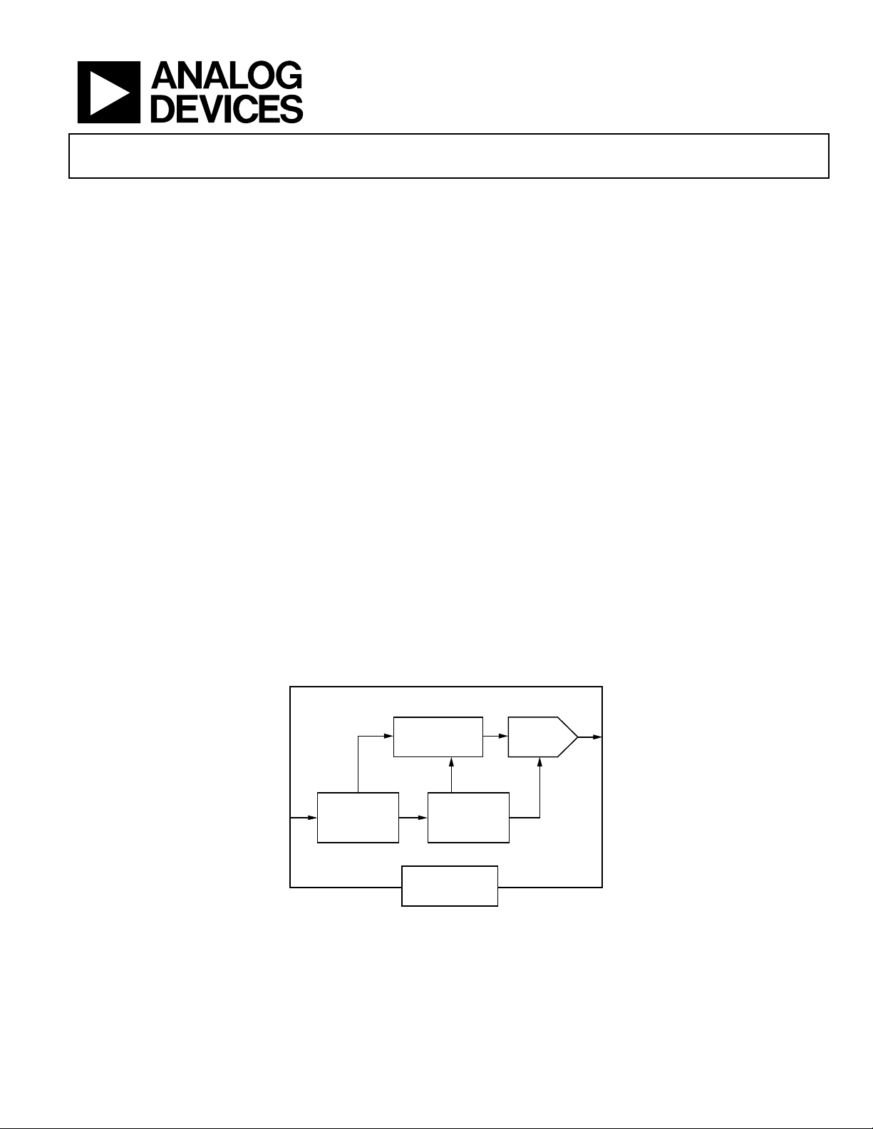
OUT
CMOS Direct Digital Synthesizer
AD9913
GENERAL DESCRIPTION
The AD9913 is a complete direct digital synthesizer (DDS)
designed to meet the stringent power consumption limits of
portable, handheld, and battery-powered equipment. The
AD9913 features a 10-bit digital-to-analog converter (DAC)
operating up to 250 MSPS. The AD9913 uses advanced DDS
technology, coupled with an internal high speed, high
performance DAC to form a complete, digitally-programmable, high frequency synthesizer capable of generating a
frequency agile analog output sinusoidal waveform at up to
100 MHz.
The AD9913 provides fast frequency hopping and fine tuning
resolution. The AD9913 also offers fine resolution phase offset
control. Control words are loaded into the AD9913 through the
serial or parallel I/O port. The AD9913 also supports a userdefined linear sweep mode of operation for generating highly
linearized swept waveforms of frequency. To support various
methods of generating a system clock, the AD9913 includes an
oscillator, allowing a simple crystal to be used as the frequency
reference, as well as a high speed clock multiplier to convert the
reference clock frequency up to the full system clock rate. For
power saving considerations, many of the individual blocks of
the AD9913 can be powered down when not in use.
The AD9913 operates over the extended industrial temperature
range of −40°C to +85°C.
FUNCTIONAL BLOCK DIAGRAM
AD9913
REF_CLK INPUT
CIRCUITRY
USER INTERFACE
Rev. A
Information furnished by Analog Devices is believed to be accurate and reliable. However, no
responsibility is assumed by Analog Devices for its use, nor for any infringements of patents or other
rights of third parties that may result from its use. Specifications subject to change without notice. No
license is granted by implication or otherwise under any patent or patent rights of Analog Devices.
Trademarks and registered trademarks are the property of their respective owners.
DDS
TIMINGAND
CONTROL LO GIC
Figure 1.
One Technology Way, P.O. Box 9106, Norwood, MA 02062-9106, U.S.A.
Tel: 781.329.4700 www.analog.com
Fax: 781.461.3113 ©2007–2010 Analog Devices, Inc. All rights reserved.
10-BIT
DAC
07002-001

AD9913
TABLE OF CONTENTS
Features .............................................................................................. 1
Applications ....................................................................................... 1
General Description ......................................................................... 1
Functional Block Diagram .............................................................. 1
Revision History ............................................................................... 2
Specifications ..................................................................................... 3
Electrical Specifications ............................................................... 3
Absolute Maximum Ratings ............................................................ 5
ESD Caution .................................................................................. 5
Equivalent Circuits ....................................................................... 5
Pin Configuration and Function Descriptions ............................. 6
Typical Performance Characteristics ............................................. 8
Applications Circuits ...................................................................... 11
Theory of Operation ...................................................................... 12
DDS Core ..................................................................................... 12
Auxiliary Accumulator .............................................................. 13
10-Bit DAC .................................................................................. 13
I/O Port ........................................................................................ 13
Profile Selections ........................................................................ 13
Modes of Operation ....................................................................... 14
Single Tone Mode ....................................................................... 14
Direct Switch Mode ................................................................... 14
Programmable Modulus Mode ................................................ 14
Linear Sweep Mode .................................................................... 14
Clock Input (REF_CLK) ................................................................ 18
REF_CLK Overview .................................................................. 18
Crystal-Driven REF_CLK ......................................................... 18
Direct-Driven REF_CLK ........................................................... 18
CMOS-Driven REF_CLK ......................................................... 18
Phase-Locked Loop (PLL) Multiplier ...................................... 18
PLL Lock Indication .................................................................. 19
Power-Down Features ................................................................ 21
I/O Programming ........................................................................... 22
Serial Programming ................................................................... 22
Parallel I/O Programming ......................................................... 23
Register Update (I/O Update) .................................................. 25
Register Map and Bit Descriptions .............................................. 26
Register Map ............................................................................... 26
Register Bit Descriptions ........................................................... 28
Outline Dimensions ....................................................................... 32
Ordering Guide .......................................................................... 32
REVISION HISTORY
6/10—Rev. 0 to Rev. A
Added Digital Input Voltage to Table 2 ......................................... 5
Added Exposed Pad Notation to Figure 3 and Table 3 ................ 5
Changes to Programmable Modulus Mode Section .................. 14
Changes to Serial Programming Section ..................................... 22
Changes to Data Write Operation Section .................................. 24
Added Register Update (I/O Update) section and Figure 35 ... 25
Added Endnote 1 to Table 9 .......................................................... 26
Changes to Register Bit Descriptions Section and Bit 7
Description in Table 10 .................................................................. 28
Changes to Table 15 and Table 16 ................................................ 31
Added Exposed Pad Notation to Outline Dimensions ............. 32
10/07—Revision 0: Initial Version
Rev. A | Page 2 of 32

AD9913
SPECIFICATIONS
ELECTRICAL SPECIFICATIONS
AVDD (1.8 V), DVDD (1.8 V), and DVDD_I/O = 1.8 V ± 5%, T = 25°C, R
reference clock frequency = 250 MHz with REF_CLK multiplier disabled, unless otherwise noted.
Table 1.
Parameter Conditions/Comments Min Typ Max Unit
REF_CLK INPUT CHARACTERISTICS
Frequency Range
REF_CLK Multiplier Disabled 250 MHz
Enabled 250 MHz
REF_CLK Input Divider Frequency Full temperature range 83 MHz
VCO Oscillation Frequency VCO1 16 250 MHz
VCO2 100 250 MHz
PLL Lock Time 25 MHz reference clock, 10× PLL 60 µs
External Crystal Mode 25 MHz
CMOS Mode VIH 0.9 V
VIL 0.65 V
Input Capacitance 3 pF
Input Impedance (Differential) 2.7 kΩ
Input Impedance (Single-Ended) 1.35 kΩ
Duty Cycle 45 55 %
REF_CLK Input Level 355 1000 mV p-p
DAC OUTPUT CHARACTERISTICS
Full-Scale Output Current 4.6 mA
Gain Error −14 −6 %FS
Output Offset +0.1 µA
Differential Nonlinearity −0.4 +0.4 LSB
Integral Nonlinearity −0.5 +0.5 LSB
AC Voltage Compliance Range
SPURIOUS-FREE DYNAMIC RANGE Refer to Figure 6
SERIAL PORT TIMING CHARACTERISTICS
SCLK Frequency 32 MHz
SCLK Pulse Width Low 17.5 ns
High 3.5 ns
SCLK Rise/Fall Time 2 ns
Data Setup Time to SCLK 5.5 ns
Data Hold Time to SCLK 0 ns
Data Valid Time in Read Mode 22 ns
PARALLEL PORT TIMING CHARACTERISTICS
PCLK Frequency 33 MHz
PCLK Pulse Width Low 10 ns
High 20 ns
PCLK Rise/Fall Time 2 ns
Address/Data Setup Time to PCLK 3.0 ns
Address/Data Hold Time to PCLK 0.3 ns
Data Valid Time in Read Mode 8 ns
IO_UPDATE/PROFILE(2:0) TIMING
Setup Time to SYNC_CLK 0.5 ns
Hold Time to SYNC_CLK 1 SYNC_CLK cycles
= 4.64 kΩ, DAC full-scale current = 2 mA, external
SET
mV
±400
Rev. A | Page 3 of 32

AD9913
Parameter Conditions/Comments Min Typ Max Unit
MISCELLANEOUS TIMING CHARACTERISTICS
Wake-Up Time1
Fast Recovery Mode 1 SYSCLK cycles2
Full Sleep Mode 60 s
Reset Pulse Width High 5 SYSCLK cycles
DATA LATENCY (PIPELINE DELAY)
Frequency, Phase-to-DAC Output Matched latency enabled 11 SYSCLK cycles
Frequency-to-DAC Output Matched latency disabled 11 SYSCLK cycles
Phase-to-DAC Output Matched latency disabled 10 SYSCLK cycles
Delta Tuning Word-to-DAC Output (Linear Sweep) 14 SYSCLK cycles
CMOS LOGIC INPUTS
Logic 1 Voltage 1.2 V
Logic 0 Voltage 0.4 V
Logic 1 Current −700 +700 nA
Logic 0 Current −700 +700 nA
Input Capacitance 3 pF
CMOS LOGIC OUTPUTS 1 mA load
Logic 1 Voltage 1.5 V
Logic 0 Voltage 0.125 V
POWER SUPPLY CURRENT
DVDD (1.8 V) Pin Current Consumption 46.5 mA
DAC_CLK_AVDD (1.8 V) 4.7 mA
DAC_AVDD (1.8 V) Pin Current Consumption 6.2 mA
PLL_AVDD (1.8 V) 1.8 mA
CLK_AVDD (1.8 V) Pin Current Consumption 4.3 mA
POWER CONSUMPTION
Single Tone Mode PLL enabled, CMOS input 50 66.5 mW
PLL disabled, differential input 57 70.5 mW
PLL enabled, XTAL input 52 68.5 mW
Modulus Mode PLL disabled 94.6 mW
Linear Sweep Mode PLL disabled 98.4 mW
Power-Down
Full 15 mW
Safe PLL enabled 44.8 mW
PLL Modes
VCO 1
Differential Input Mode 11 mW
CMOS Input Mode 7.5 mW
Crystal Mode 5.4 mW
VCO 2
Differential Input Mode 15 mW
CMOS Input Mode 11.5 mW
Crystal Mode 9.4 mW
1
Refer to the Power-Down Features section.
2
SYSCLK cycle refers to the actual clock frequency used on-chip by the DDS. If the reference clock multiplier is used to multiply the external reference clock frequency,
the SYSCLK frequency is the external frequency multiplied by the reference clock multiplication factor. If the reference clock multiplier and divider are not used, the
SYSCLK frequency is the same as the external reference clock frequency.
Rev. A | Page 4 of 32
AD9913
A
C
ABSOLUTE MAXIMUM RATINGS
Table 2.
Parameter Rating
Maximum Junction Temperature 150°C
AVDD, DVDD 2 V
Digital Input Voltage −0.7 V to +2.2 V
Digital Output Current 5 mA
Storage Temperature –65°C to +150°C
Operating Temperature –40°C to +105°C
Lead Temperature (Soldering, 10 sec) 300°C
θJA 36.1°C/W
θJC 4.2°C/W
Stresses above those listed under Absolute Maximum Ratings
may cause permanent damage to the device. This is a stress
rating only and functional operation of the device at these or
any other conditions above those indicated in the operational
section of this specification is not implied. Exposure to absolute
maximum rating conditions for extended periods may affect
device reliability.
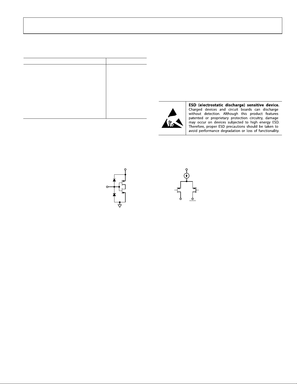
ESD CAUTION
EQUIVALENT CIRCUITS
DIGITAL INPUTS
INPUT
VOID OVERDRIVING DIGITAL INPUTS.
FORWARD BIASING ESD DIO DES M AY
OUPLE DIGIT AL NOISE ONTO P O WER
PINS.
DVDD_I/O
Figure 2. Equivalent Input and Output Circuits
DAC OUTPUTS
AVDD
IOUT IOUT
MUST TERMI NATE OUTPUT S TO AGND
FOR CURRENT FLOW. DO NOT EXCEED
THE OUTPUT V OLTAGE COMPLIANCE
RATING.
07002-002
Rev. A | Page 5 of 32
AD9913
PIN CONFIGURATION AND FUNCTION DESCRIPTIONS
D)
RESET
N_CTL
R/R
ADR6/D6
ADR7/D7
SCLK(PCLK)
SDIO(W
CS
IO_UPDATE
PWR_DW
MASTER_
29
28
27
26
31
30
32
25
1PS2/ADR5/D5
PIN 1
2PS1/ADR4/D4
INDICATOR
3PS0/ADR3/D3
4DVDD
AD9913
5DGND
TOP VIEW
6ADR2/D2
(Not to S cale)
7ADR1/D1
8ADR0/D0
9
11
10
12
13
R
CLK
CLK
_
_
AVDD
AGND
SER/PA
REF
SYNC
NOTES
1. EXPOSE D PAD SHOULD BE SO LDERED TO G ROUND.
24 RSET
23 AGND
22 AVDD
21 AGND
20 IOUT
19 IOUT
18 AGND
17 AVDD
14
15
16
CLK
GND
_
AVDD
A
REF
07002-003
Figure 3. Pin Configuration
Table 3. Pin Function Descriptions
Pin No. Mnemonic I/O Description
1 PS2/ADR5/D5 I/O
Multipurpose pin: Profile Select Pin (PS2) in Direct Switch Mode, Parallel Port Address Line (ADR5), and
Data Line (D5) to program registers.
2 PS1/ADR4/D4 I/O
Multipurpose pin: Profile Select Pin (PS1) in Direct Switch Mode or Linear Sweeping Mode, Parallel Port
Address Line (ADR4), and Data Line (D4) to program registers.
3 PS0/ADR3/D3 I/O
Multipurpose pin: Profile Select Pin (PS0) in Direct Switch Mode or Linear Sweeping Mode, Parallel Port
Address Line (ADR3), and Data Line (D3) to program registers.
4 DVDD I Digital Power Supply (1.8 V).
5 DGND I Digital Ground.
6 ADR2/D2 I/O Parallel Port Address Line 2 and Data Line 2.
7 ADR1/D1 I/O Parallel Port Address Line 1and Data Line 1.
8 ADR0/D0 I/O Parallel Port Address Line 0 and Data Line 0.
9 SYNC_CLK O
Clock Out. The profile pins [PS0:PS2] and the IO_UPDATE pin (Pin 27) should be set up to the rising
edge of this signal to maintain constant pipe line delay through the device.
10
11, 15,
/PAR
SER
AGND I Analog Ground.
I Serial Port and Parallel Port Selection. Logic low = serial mode; logic high = parallel mode.
18, 21,
23
12, 16,
AVDD I Analog Power Supply (1.8 V).
17, 22
13 REF_CLK I Reference Clock Input. See the REF_CLK Overview section for more details.
14
19
REF_CLK
IOUT
I Complementary Reference Clock Input. See the REF_CLK Overview section for more details.
O Open Source DAC Complementary Output Source. Current mode. Connect through 50 Ω to AGND.
20 IOUT O Open Source DAC Output Source. Current mode. Connect through 50 Ω to AGND.
24 RSET I
Analog Reference. This pin programs the DAC output full-scale reference current. Attach a 4.64 kΩ
resistor to AGND.
25 MASTER_RESET I
Master Reset, Digital Input (Active High). This pin clears all memory elements and reprograms registers
to default values.
Rev. A | Page 6 of 32
AD9913
Pin No. Mnemonic I/O Description
26 PWR_DWN_CTL I
27 IO_UPDATE I
28
29
30 SCLK/PCLK I Input Clock for Serial and Parallel Port.
31 ADR7/D7 I/O Parallel Port Address Line 7 and Data Line 7.
32 ADR6/D6 I/O Parallel Port Address Line 6 and Data Line 6.
33 Exposed Paddle The EPAD should be soldered to ground.
CS
SDIO(WR
/RD)
External Power-Down, Digital Input (Active High). A high level on this pin initiates the currently
programmed power-down mode. See the Power-Down Features section for further details. If unused,
tie to ground.
I/O Update; Digital Input. A high on this pin indicates a transfer of the contents of the I/O buffers to the
corresponding internal registers.
I
Chip Select for Serial and Parallel Port. Digital input (active low). Bringing this pin low enables the
AD9913 to detect serial (SCLK) or parallel (PCLK) clock rising/falling edges. Bringing this pin high
causes the AD9913 to ignore input on the data pins.
I/O Bidirectional Data Line for Serial Port Operation and Write/Read Enable for Parallel Port Operation.
Rev. A | Page 7 of 32
AD9913
–
–
TYPICAL PERFORMANCE CHARACTERISTICS
0
−10
−20
−30
−40
−50
−60
POWER (d Bm)
−70
−80
−90
−100
0 20406080100120
FREQUENCY (MHz)
Figure 4. Wideband SFDR @ 99.76 MHz f
OUT
(250 MHz Clock, 4 mA DAC Full-Scale Current, PLL Bypassed)
0
−10
−20
−30
−40
−50
−60
POWER (d Bc)
−70
−80
−90
−100
0 20406080100120
FREQUENCY (MHz)
Figure 5. Wideband SFDR @ 25.14 MHz f
OUT
(250 MHz Clock, 4 mA DAC Full-Scale Current, PLL Bypassed)
50
07002-004
07002-005
0
−20
−40
−60
SFDR (dBm)
−80
−100
−120
99.758381 99.783381
99.763381 99.768381 99.773381 99.778381
FREQUENCY (MHz )
Figure 7. Narrow-Band SFDR @ 99.76 MHz f
OUT
(250 MHz Clock, 4 mA DAC Full-Scale Current, PLL Bypassed)
0
−20
−40
−60
SFDR (dBm)
−80
−100
−120
25.124918 25.17491825.134918 25.144918 25.154918 25.164918
25.129918 25.139918 25.149918 25.159918 25.169918
Figure 8. Narrow-Band SFDR @ 25.14 MHz f
FREQUENCY (MHz )
OUT
(250 MHz Clock, 4 mA DAC Full-Scale Current, PLL Bypassed)
50
07002-007
07002-008
–55
–60
–65
–70
SFDR (dBc)
–75
–80
–85
–90
00
0.05 0.10 0.15 0.20 0.25 0.30 0.35 0.40
f
(% of System Cl o ck)
OUT
1.9V
1.7V
1.8V
07002-031
.45
Figure 6. SFDR vs. Supply Variation
(250 MHz Clock, 4 mA DAC Full-Scale Current, PLL Bypassed)
–55
–60
–65
–70
SFDR (dBc)
–75
–80
–85
–90
00
0.05 0.10 0.15 0.20 0.25 0.30 0.35 0.40
f
OUT
+85ºC
+25°C
(% of System Clock)
–40°C
07002-032
.45
Figure 9. SFDR vs. Temperature
(250 MHz Clock, 4 mA DAC Full-Scale Current, PLL Bypassed)
Rev. A | Page 8 of 32
AD9913
–
–
–
50
–55
–60
–65
–70
SFDR (dBc)
–75
–80
–85
–90
0 250
50 100 150 200
39.88%
10.21%
SYSTEM CLO CK (MHz )
Figure 10. SFDR vs. System Clock Frequency (PLL Bypassed)
100
–110
–120
–130
–140
–150
PHASE NOISE (dBc/Hz)
–160
–170
100 1k 10k 100k 1M 10M
10 100M
FREQUENCY (MHz)
26.58%
92.3MHz
48.9MHz
23.1MHz
6.1MHz
−50
−60
−70
−80
−90
−100
−110
−120
PHASE NOISE (dBc/Hz)
−130
−140
07002-033
−150
100 100M
1k 10k 100k 1M 10M
FREQUENCY (MHz)
Figure 12. Absolute Phase Noise vs. f
99MHz
49MHz
25MHz
12.5MHz
Using the Internal PLL
OUT
07002-012
(REF_CLK 25 MHz × 10 = 250 MHz Using PLL)
50
–55
–60
–65
–70
SFDR (dBc)
–75
–80
–85
07002-042
–90
00
0.05 0.10 0.15 0.20 0.25 0.30 0.35 0.40
f
OUT
REFSPUR
(% of System Clock)
BYPASS
PLL ×10
07002-034
.45
Figure 11. Residual Phase Noise vs. f
(PLL Bypassed)
OUT
Figure 13. SFDR Without the Internal PLL
(REF_CLK = 25 MHz × 10 = 250 MHz Using PLL, 4 mA DAC Full-Scale Current)
Rev. A | Page 9 of 32
AD9913
80
−60
−80
VCO 1
−100
VCO 2
−120
PHASE NOISE ( dBc/Hz)
−140
−160
100 100M
1k 10k 100k 1M 10M
FREQUENCY (MHz)
Figure 14. Absolute Phase Noise, VCO1 vs. VCO2
40
35
30
25
20
15
DVDD
AVDD (PLL)
AVDD (CLK)
AVDD (DAC)
AVDD (DAC CLK)
70
60
CMOS INPUT LINEAR SWEEP
50
40
30
20
TOTAL P OWER DISSI P ATED (mW)
10
07002-011
0
50 250
DIFF INP UT LINEAR SWE E P
DIFF INPUT SINGLE TONE
CMOS INPUT SINGLE T O NE
70 90 110 130 150 170 190 210 230
SYSTEM CLOCK FREQUENCY (M Hz )
07002-036
Figure 16. Power Dissipation vs. System Clock Frequency
vs. Clock Input Mode
10
POWER DISSIPATION (mW)
5
0
70 90 110 130 150 170 190 210 230
50 250
SYSTEM CLOCK FREQUENCY (M Hz )
Figure 15. Power Supply Current Domains
(CMOS Input Mode, 4 mA DAC Full-Scale Current, Single Tone)
07002-035
Rev. A | Page 10 of 32

AD9913
APPLICATIONS CIRCUITS
LO
AD9913
SIDEBAND
SELECTION
FILTER
SPLITTER
+
–
–
+
–
–
+
+
ADC
07002-013
Figure 17. RFID Block Diagram (Only I-Channel of Receiver Shown)
INPUT
LOW-PASS
FILTER
INPUT
ATTENUATOR
AD9913 AS
GENERATOR
LOCAL
OSCILLATOR
SWEEP
SIGNAL
BAND-PASS
FILTER
VGA
+
–
VIDEO
FILTER
CRT DISPLAY
07002-014
Figure 18. Handheld Spectrum Analyzer
Rev. A | Page 11 of 32

AD9913
THEORY OF OPERATION
DDS CORE
The DDS block generates a reference signal (sine or cosine
based on the selected DDS sine output bit). The parameters of
the reference signal (frequency and phase), are applied to the
DDS at its frequency and phase offset control inputs, as shown
in Figure 19.
DDS SIGNAL CO NTROL PARAMETERS
PHASE
14
OFFSET
CONTROL
FREQUENCY
CONTROL
32
SYSTEM
CLOCK
The output frequency (f
frequency tuning word (FTW) at the frequency control input to
the DDS. In all modes except for programmable modulus, the
relationship between f
FTW
⎛
f
=
⎜
OUT
where
FTW is a 32-bit integer ranging in value from 0 to
2,147,483,647 (2
32
2
⎝
31
full 32-bit range. This range constitutes frequencies from dc to
Nyquist (that is, ½ f
MSB ALIGNED
32-BIT
ACCUMULATOR
32
32
DQ
15
32
R
ACCUMULATOR
RESET
MSBs
15
CONVERSION
ANGLE
TO
AMPLITUDE
(SINE OR
COSINE)
10
TO DAC
Figure 19. DDS Block Diagram
) of the AD9913 is controlled by the
OUT
⎞
⎟
⎠
OUT
f
SYSCLK
, FTW, and f
(1)
SYSCLK
is:
− 1), which represents the lower half of the
).
SYSCLK
f
The FTW required to generate a desired value of
is found
OUT
by solving Equation 1 for FTW as given in Equation 2
FTW
⎛
⎛
32
⎜
=
⎜
2round (2)
⎜
⎜
f
⎝
⎝
f
OUT
SYSCLK
⎞
⎞
⎟
⎟
⎟
⎟
⎠
⎠
where the round(x) function rounds the argument (the value of
x) to the nearest integer. This is required because the FTW is
constrained to be an integer value.
For applications where rounding to the nearest available frequency is not acceptable, programmable modulus mode enables
additional options.
The relative phase of the DDS signal can be digitally controlled
by means of a 14-bit phase offset word (POW). The phase offset
is applied prior to the angle-to-amplitude conversion block
internal to the DDS core. The relative phase offset (Δθ) is given by
07002-030
POW
⎞
⎛
2
π
=θΔ
360
⎜
⎝
2
POW
⎛
⎜
⎝
⎟
14
⎠
⎞
⎟
14
2
⎠
where the upper quantity is for the phase offset expressed as
radian units and the lower quantity as degrees. To find the
POW value necessary to develop an arbitrary Δθ, solve the
above equation for POW and round the result (in a manner
similar to that described for finding an arbitrary FTW in
Equation 1 and Equation 2).
AUXILIARY
ACCUMULATOR
32 32
CLOCK PORT
REF_CLK
REF_CLK
PHASE
ACCUMULATOR
32
0
+
–1
1
32
1
0
EXTERNAL
FTW POW
PLL
MULTIPLIER
Z
0
PROFILE
SELECTIONS
1
2
INTERNAL
REGISTE R MAP AND TIMING CONTROL
CLOCK
SELECTION
DDS CORE
0
1
32 14
PHASE
OFFSET
14
0
SER/PAR
1
ANGLE TO
AMPLITUDE
I/O PORT
CS
SCLK/PCLK
SDIO (WR/RD)
DAC
10
AD[7:0]/PS[2:0]
PWR_DWN_CTL
MASTER RESET
IOUT
IOUT
RSET
07002-015
SYNC_CLK
IO_UPDATE
Figure 20. Detailed Block Diagram
Rev. A | Page 12 of 32

AD9913
AUXILIARY ACCUMULATOR
In addition to the phase accumulator of the DDS, the AD9913
has an auxiliary accumulator. This accumulator can be configured to support either an automatic sweep of one of the
programmable characteristics of the DDS output (frequency or
phase), or it can be configured to implement a change in the
denominator of the frequency equation given in the DDS Core
section. For further details, refer to the Programmable Modulus
Mode section.
10-BIT DAC
The AD9913 incorporates an integrated 10-bit, current output
DAC. The output current is delivered as a balanced signal using
two outputs. The use of balanced outputs reduces the potential
amount of common-mode noise present at the DAC output,
offering the advantage of an increased signal-to-noise ratio. An
external resistor (R
AGND establishes the reference current. The full-scale output
current of the DAC (I
reference current. The recommended value of R
The following equation computes the typical full-scale current
with respect to the R
setting:
RxI
The DAC is designed to operate with full-scale current values
up to 4.58 mA. Based on the equation and assuming a 4.62 kΩ
resistor value for R
current for the DAC is 2.28 mA.
Figure 17 shows the range of DAC output current vs. the DAC
FS value assuming an R
) connected between the RSET pin and
SET
) is produced as a scaled version of the
OUT
resistor value and the gain control
set
0206.0
()
x
),(
SETOUT
R
SET
, and x = 0x1FF, the nominal output
SET
SET
+×= 1
value of 4.62 kΩ.
is 4.62 kΩ.
SET
5
4
3
2
1
DAC FULL-SCAL E CURRE NT (mA)
0
0 1200
200 400 600 800 1000
DAC CODE
Figure 21. DAC Output Current vs. DAC FS Bits
07002-016
Pay careful attention to the load termination to ensure that the
output voltage remains within the specified compliance range;
voltages developed beyond this range cause excessive distortion
and can damage the DAC output circuitry.
I/O PORT
The AD9913 I/O port can be configured as a synchronous serial
communications port that allows easy interface to many industrystandard microcontrollers and microprocessors. The serial I/O port
is compatible with most synchronous transfer formats, including
both the Motorola 6905/11 SPI and Intel 8051 SSR protocols. For
faster programming requirements, a parallel mode is also provided.
PROFILE SELECTIONS
The AD9913 supports the use of profiles, which consist of a group
of eight registers containing pertinent operating parameters for
a particular operating mode. Profiles enable rapid switching
between parameter sets. Profile parameters are programmed via
the I/O port. Once programmed, a specific profile is activated
by means of Register CFR1 Bits [22:20], or three external profile
select pins. The external profile pins option is only available in
serial mode.
Rev. A | Page 13 of 32

AD9913
MODES OF OPERATION
The AD9913 operates in four modes:
• Single tone
• Direct switch
• Programmable modulus
• Linear sweep
The modes relate to the data source used to supply the DDS
with its signal control parameters: frequency, phase, or amplitude. The partitioning of the data into different combinations
of frequency, phase, and amplitude is handled automatically
based on the mode and/or specific control bits.
SINGLE TONE MODE
Single tone mode is the default operational mode and is active
when both the direct switch mode bit and the auxiliary
accumulator enable bit are not set. This mode outputs a single
frequency as programmed by the user in the frequency tuning
word (FTW) register. A phase offset value is also available in
single tone mode via the POW register.
DIRECT SWITCH MODE
Direct switch mode enables FSK or PSK modulation. This mode
simply selects the frequency or phase value programmed into
the profile registers. Frequency or phase is determined by the
destination bits in CFR1 [13:12]. Direct switch mode is enabled
using the direct switch mode active bit in register CFR1 [16].
Two approaches are designed for switching between profile
registers. The first is programming the internal profile control
bits, CFR1 [22:20], to the desired value and issuing an
IO_UPDATE. The second approach, with higher data
throughput, is achieved by changing the profile control pins
[2:0]. Control bit CFR1 [27] is for selection between the two
approaches. The default state uses the profile pins.
To perform 8-tone FSK or PSK, program the FTW word or
phase offset word in each profile. The internal profile control
bits or the profile pins are used for the FSK or PSK data.
Tabl e 4 shows the relationship between the profile selection pin
or bit approach.
Table 4. Profile Selection
Profile Pins PS [2:0] or CFR1 Bits [22:20] Profile Selection
000 Profile 0
001 Profile 1
010 Profile 2
011 Profile 3
100 Profile 4
101 Profile 5
110 Profile 6
111 Profile 7
PROGRAMMABLE MODULUS MODE
In programmable modulus mode, the auxiliary accumulator is
used to alter the frequency equation of the DDS core, making it
possible to implement fractions which are not restricted to a
power of 2 in the denominator.
A standard DDS is restricted to powers of 2 as a denominator
because the phase accumulator is a set of bits as wide as the
frequency tuning word. When in programmable modulus
mode, the frequency equation becomes
= (FTW)(fS)/x with 0 ≤ FTW ≤ 2
f
0
f0 = fS × (1 − (FTW/x)) with 2
where 0 ≤ x ≤ 232.
When in programmable modulus mode, the auxiliary accumulator is set up to roll over before it reaches full capacity. Every
time it rolls over, an extra LSB value is added to the phase
accumulator. In order to determine the values that must be
programmed in the registers, the user must define the desired
output to sampling clock frequency as a ratio of integers (M/N,
where N must not exceed 2
Refer to the AN-953 Application Note for detailed steps of how
to implement a programmable modulus. The AN-953 defines
how to calculate the three required values (A, B, and X) used for
programmable modulus. The following assigns the required
values to the appropriate register.
• Register 0x06 [63:32] holds the B value.
• Register 0x06 [31:0] holds the X value.
• Register 0x07 [31:0] holds the A value.
LINEAR SWEEP MODE
One purpose of linear sweep mode is to provide better
bandwidth containment compared to direct switch mode by
enabling more gradual, user-defined changes between a starting
point (S0) to an endpoint (E0). The auxiliary accumulator
enable bit is located in Register CFR1 [11]. Linear sweep uses
the auxiliary accumulator to sweep frequency or phase from S0
to E0. A frequency or phase sweep is determined by the
destination bits in CFR1 [13:12]. The trigger to initiate the
sweep can be edge or level triggered. This is determined by
Register CFR1 [9]. Note that, in level triggered mode, the sweep
automatically repeats as long as the appropriate profile pin is
held high.
In linear sweep mode, S0 and E0 (upper and lower limits) are
loaded into the linear sweep parameter register (Register 0x06).
If configured for frequency sweep, the resolution is 32-bits. For
phase sweep, the resolution is 14 bits. When sweeping the
phase, the word value must be MSB-aligned; unused bits are
ignored. The profile pins or the internal profile bits trigger and
control the direction (up/down) of the linear sweep for
frequency or phase. Tab le 5 depicts the direction of the sweep.
31
31
< FTW < 2
32
).
32
− 1
Rev. A | Page 14 of 32

AD9913
(
=
Δ
Table 5. Determining the Direction of the Linear Sweep
Profile Pins [2:0] or CFR1 Bits [22:20] Linear Sweep Mode
x001 Sweep off
x011 Ramp up
1
x10
Ramp down
x111 Bidirectional ramp
1
x = don’t care.
Note that if the part is used in parallel port programming mode,
the sweep mode is only determined by the internal profile
control bits, CFR1 [22:20]. If the part is used in serial port
programming mode, either the internal profile control bits or
the external profile select pins can work as the sweep control.
CFR1 [27] selects between these two approaches.
Setting the Slope of the Linear Sweep
The slope of the linear sweep is set by the intermediate step size
(delta tuning word) between S0 and E0 (see Figure 22) and the
time spent (sweep ramp rate word) at each step. The resolution
of the delta tuning word is 32 bits for frequency and 14 bits for
phase. The resolution for the delta ramp rate word is 16 bits.
In linear sweep mode, the user programs a rising delta word
(RDW, Register 0x07) and a rising sweep ramp rate (RSRR,
Register 0x08). These settings apply when sweeping from S0 to
E0. The falling delta word (FDW, Register 0x07) and falling
sweep ramp rate (FSRR, Register 0x08) apply when sweeping
from E0 to S0.
Note that if the auxiliary accumulator is allowed to overflow, an
uncontrolled, continuous sweep operation occurs. To avoid this,
the magnitude of the rising or falling delta word should be
smaller than the difference between full-scale and the E0 value
32
(full-scale − E0). For a frequency sweep, full-scale is 2
14
a phase sweep, full-scale is 2
− 1.
− 1. For
Figure 22 displays a linear sweep up and then down. This
depicts the dwell mode (see CRF1 [8]). If the no-dwell bit,
CFR1 [8], is set, the sweep accumulator returns to 0 upon
reaching E0.
E0
For a piecemeal or a nonlinear transition between S0 and E0,
the delta tuning words and ramp rate words can be reprogrammed during the transition.
The formulas for calculating the step size of RDW or FDW are
RDW
⎛
=
StepFrequency
π
RDW
⎛
=
StepPhase (radians)
⎜
2
⎝
45RDW
⎛
=
StepPhase (degrees)
⎜
2
⎝
⎞
⎜
⎟
32
2
⎝
⎠
⎞
⎟
13
⎠
⎞
⎟
11
⎠
(MHz)
f
SYSCLK
The formula for calculating delta time from RSRR or FSRR is
)
At 250 MSPS operation, (f
fRSRRt
SYSCLK
(Hz)/
=250 MHz). The minimum time
SYSCLK
interval between steps is 1/250 MHz × 1 = 4 ns. The maximum
time interval is (1/250 MHz) × 65,535= 262 μs.
Frequency Linear Sweep Example
In linear sweep mode, when sweeping from low to high, the
RDW is applied to the input of the auxiliary accumulator and
the RSRR register is loaded into the sweep rate timer.
The RDW accumulates at the rate given by the ramp rate
(RSRR) until the output equals the upper limit in the linear
sweep parameter register (Register 0x06). The sweep is then
complete.
When sweeping from high to low, the FDW is applied to the
input of the auxiliary accumulator and the FSRR register is
loaded into the sweep rate timer.
The FDW accumulates at the rate given by the ramp rate
(FSRR) until the output equals the lower limit in the linear
sweep parameter register value (Register 0x06). The sweep is
then complete. A phase sweep works in the same manner with
fewer bits.
To view sweep capabilities using the profile pins and the nodwell bit, refer to Figure 23, Figure 24, and Figure 25.
RDW FDW
Δf, p Δf, p
LINEAR SWEE P
(FREQUENCY/PHASE)
S0
RSRR FSRR
TIME
Figure 22. Linear Sweep Mode
ΔtΔt
07002-037
Rev. A | Page 15 of 32

AD9913
RAMP-UP MODE (EDGE TRIG GERED)
PS[0]
PS[1]
PS[0]
PS[1]
PS[0]
PS[1]
PS[0]
PS[1]
E0
S0
E0
S0
E0
S0
E0
S0
NO-DWELL BIT = 0
NO-DWELL BIT = 1
RAMP-UP MODE (LEVEL TRIGGERED)
NO-DWELL
BIT = 0
NO-DWELL
BIT = 1
PS[0]
PS[1]
PS[0]
PS[1]
PS[0]
PS[1]
PS[0]
PS[1]
07002-040
E0
S0
E0
S0
E0
S0
E0
S0
RAMP-DOWN MO DE ( E DGE TRIGGERED)
NO-DWELL BIT = 0
NO-DWELL BIT = 1
RAMP-DO WN MODE (LEV EL TRIGGER ED)
NO-DWELL BIT = 0
NO-DWELL BIT = 1
07002-041
Figure 23. Display of Ramp-Up and Ramp-Down Capability Using the External Profile Pins
Rev. A | Page 16 of 32

AD9913
E0
S0
PS[0]
PS[1]
E0
S0
PS[0]
PS[1]
E0
S0
PS[0]
PS[1]
BIDIRECTIONAL MODE (E DG E TRIGG ERE D)
NO-DWELL BIT = x
BIDIRECTIONAL MODE (LEVEL TRIGGERED)
NO-DWELL BIT = 0
NO-DWELL BIT = 1
Figure 24. Display of Bidirectional Ramp Capability
Using the External Profile Pins
COMBINATI ON OF MODE S ( E DGE TRIGG ERED)
RAMP UP
MODE
RAMP DOWN
MODE
BIDIRECTIONAL
MODE
RAMP UP
MODE
07002-044
E0
S0
PS[0]
PS[1]
Figure 25. Combination of Sweep Modes Using the External Profile Pins
Clear Functions
The AD9913 allows for a programmable continuous zeroing of
the sweep logic and the phase accumulator as well as clear-andrelease, or automatic zeroing function. Each feature is
individually controlled via bits in the control registers.
Continuous Clear Bits
The continuous clear bits are simply static control signals that
hold the respective accumulator (and associated logic) at zero
for the entire time the bit is active.
Clear-and-Release Function
The auto clear auxiliary accumulator bit, when active, clears and
07002-043
releases the auxiliary accumulator upon receiving an
I/O_UPDATE or change in profile bits.
The auto clear phase accumulator, when active, clears and
releases the phase accumulator upon receiving a I/O_UPDATE
or a change in profile bits.
The automatic clearing function is repeated for every
subsequent I/O_UPDATE or change in profile bits until the
control bit is cleared.
These bits are programmed independently and do not have to
be active at the same time. For example, one accumulator may
be using the clear and release function while the other is
continuously cleared.
Rev. A | Page 17 of 32

AD9913
S
R
CLOCK INPUT (REF_CLK)
REF_CLK OVERVIEW
The AD9913 supports a number of options for producing the
internal SYSCLK signal (that is, the DAC sample clock) via the
REF_CLK input pins. The REF_CLK input can be driven
directly from a differential or single-ended source, or it can
accept a crystal connected across the two input pins. There is
also an internal phase-locked loop (PLL) multiplier that can be
independently enabled. The various input configurations are
controlled by means of the control bits in the CFR2 [7:5]
register.
Table 6. Clock Input Mode Configuration
CFR2 [7:5] Mode Configuration
000 Differential Input, PLL Enabled
001 Differential Input, PLL Disabled (Default)
x101 XTAL Input, PLL Enabled
x111 XTAL Input, PLL Disabled
100 CMOS Input, PLL Enabled
101 CMOS Input PLL Disabled
1
x = don’t care.
CFR2[15]
÷2
07002-021
0
1
CFR2[5]
1
0
SYSTEM
CLOCK
CFR2[6]
CFR2[7:6]
REF_CLK
REF_CLK
13
14
XTAL
DIFFERENTIAL/
SINGLE
CMOS
1
0
CFR2[3]
00
10
÷2
PLL
0
1
DIVIDE
CONTROL
CFR2[5:0]CFR2[14:9]
Figure 26. Internal Clock Path Functional Block Diagram
CRYSTAL-DRIVEN REF_CLK
When using a crystal at the REF_CLK input, the resonant
frequency should be approximately 25 MHz. Figure 27 shows
the recommended circuit configuration.
13
REFCLK
XTAL
14
39pF39pF
Figure 27. Crystal Connection Diagram
REFCLK
DIRECT-DRIVEN REF_CLK
When driving the REF_CLK inputs directly from a signal
source, either single-ended or differential signals can be used.
With a differential signal source, the REF_CLK pins are driven
with complementary signals and ac-coupled with 0.1 μF
capacitors. With a single-ended signal source, either a singleended-to-differential conversion can be employed or the
REF_CLK input can be driven single-ended directly. In either
case, 0.1 μF capacitors are used to ac couple both REF_CLK
pins to avoid disturbing the internal dc bias voltage of ~1.35 V.
See Figure 28 for more details.
The REF_CLK input resistance is ~2.7 kΩ differential (~1.35 kΩ
single-ended). Most signal sources have relatively low output
impedances. The REF_CLK input resistance is relatively high,
therefore, its effect on the termination impedance is negligible
and can usually be chosen to be the same as the output impedance of the signal source. The bottom two examples in Figure 28
assume a signal source with a 50 Ω output impedance.
0.1µF
DIFFERENT IAL SOURCE,
DIFFERENTIAL INPUT
SINGLE- ENDE D SO URCE,
DIFFERENTIAL INPUT
INGLE-ENDED SOURCE,
SINGLE-ENDED INPUT
LVPECL,
OR
LVDS
DRIVER
BALUN
(1:1)
50Ω
TERMINATION
0.1µF
0.1µF
50Ω
0.1µF
0.1µF
0.1µF
Figure 28. Direct Connection Diagram
07002-020
CMOS-DRIVEN REF_CLK
REF_CLK
13
14
REF_CLK
13
REF_CLK
14
REF_CLK
13
REF_CLK
14
REF_CLK
07002-022
This mode is enabled by writing CFR2 [7] to be true. In this
state, the AD9913 must be driven at Pin 13 with the reference
clock source. Additionally, it is recommended that Pin 14 in
CMOS mode be tied to ground through a 10 kΩ resistor.
13
CMOS
DRIVE
10kΩ
REF_CLK
14
REF_CLK
7002-023
Figure 29. CMOS-Driven Diagram
PHASE-LOCKED LOOP (PLL) MULTIPLIER
An internal phase-locked loop (PLL) provides users of the
AD9913 the option to use a reference clock frequency that is
lower than the system clock frequency. The PLL supports a wide
range of programmable frequency multiplication factors (1× to
64×). See Tabl e 7 for details on configuring the PLL multiplication factor. The PLL is also equipped with a PLL_LOCK bit.
CFR2 [15:8] and CFR2 [5:1] control the PLL operation. Upon
power-up, the PLL is off. To initialize the PLL, CFR2 [5] must
be cleared and CFR2 [1] must be set. The function of CFR2 [1]
Rev. A | Page 18 of 32

AD9913
is to reset digital logic in the PLL circuit with an active low
signal. The function of CFR2 [5] is to power up or power down
the PLL.
CFR2 [4] is the PLL LO range bit. When operating the AD9913
with the PLL enabled, CFR2 [4] adjusts PLL loop filter
components to allow low frequency reference clock inputs.
CFR2 [3] enables a divide-by-two circuit at the input of the PLL
phase detector. If this bit is enabled the reference clock signal is
divided by 2 prior to multiplication in the PLL. Refer to the
electrical specifications for the maximum reference clock input
frequency when utilizing the PLL with the divide by 2 circuit
enabled. If the divide by 2 circuit is disabled and the PLL is
enabled, then the maximum reference clock input frequency is
one-half the maximum rate indicated in the electrical
specifications table for the maximum input divider frequency.
The AD9913 PLL uses one of two VCOs for producing the
system clock signal. CFR2 Bit 2 is a select bit that enables an
alternative VCO in the PLL. The basic operation of the PLL is
not affected by the state of this bit. The purpose of offering two
VCOs is to provide performance options. The two VCOs have
approximately the same gain characteristics, but differ in other
aspects. The overall spurious performance, phase noise, and
power consumption may change based on the setting of CFR2
Bit 2. It is important to consider that for either VCO, the
minimum oscillation frequency must be satisfied, and that
minimum oscillation frequency is significantly different
between the two oscillators.
CFR2 [15:9], along with CFR2 [3], determine the multiplication
of the PLL. CFR2 [15] enables a divider at the output of the
PLL. The bits CFR [14:9] control the feedback divider. The
feedback divider is composed of two stages: ÷ N (1:31) selected
by CFR2 [13:9];
Note that the same system clock frequency can be obtained with
different combinations of CFR2 [15:9] and CFR2 [3]. One
combination may work better in a given application either to
run at lower power or to satisfy the VCOs minimum oscillation
frequency
Note that the AD9913 maximum system clock frequency is
250 MHz. If the user intends to use high values for the PLL
feedback divider ratio, then care should be taken that the
system clock frequency does not exceed 250 MHz.
÷1 or ÷2 selected by CFR2 [14].
PLL LOCK INDICATION
CFR2 [0] is a read-only bit that displays the status of the PLL
lock signal.
When the AD9913 is programmed to use the PLL, there is some
amount of time required for the loop to lock. While the loop is
not locked, the chip system clock operates at the reference clock
frequency presented to the part at the pins. Once the PLL lock
signal goes high, the system clock frequency switches
asynchronously to operate at the PLL output frequency. To
maintain a system clock frequency with or without a locked
loop if the PLL lock signal transistions low, the chip reverts to
the reference clock signal while the loop attempts to acquire
lock once again.
Tabl e 7 describes how to configure the PLL multiplication factor
using the appropriated register bits.
Rev. A | Page 19 of 32

AD9913
Table 7. PLL Multiplication Factor Configuration
CFR2 [15:14], CFR2 [3]
CFR2 [13:9]
00000 32 16 16 8 64 32 32 16
00001 1 0.5 0.5 0.25 2 1 1 0.5
00010 2 1 1 0.5 4 2 2 1
00011 3 1.5 1.5 0.75 6 3 3 1.5
00100 4 2 2 1 8 4 4 2
00101 5 2.5 2.5 1.25 10 5 5 2.5
00110 6 3 3 1.5 12 6 6 3
00111 7 3.5 3.5 1.75 14 7 7 3.5
01000 8 4 4 2 16 8 8 4
01001 9 4.5 4.5 2.25 18 9 9 4.5
01010 10 5 5 2.5 20 10 10 5
01011 11 5.5 5.5 2.75 22 11 11 5.5
01100 12 6 6 3 24 12 12 6
01101 13 6.5 6.5 3.25 26 13 13 6.5
01110 14 7 7 3.5 28 14 14 7
01111 15 7.5 7.5 3.75 30 15 15 7.5
10000 16 8 8 4 32 16 16 8
10001 17 8.5 8.5 4.25 34 17 17 8.5
10010 18 9 9 4.5 36 18 18 9
10011 19 9.5 9.5 4.75 38 19 19 9.5
10100 20 10 10 5 40 20 20 10
10101 21 10.5 10.5 5.25 42 21 21 10.5
10110 22 11 11 5.5 44 22 22 11
10111 23 11.5 11.5 5.75 46 23 23 11.5
11000 24 12 12 6 48 24 24 12
11001 25 12.5 12.5 6.25 50 25 25 12.5
11010 26 13 13 6.5 52 26 26 13
11011 27 13.5 13.5 6.75 54 27 27 13.5
11100 28 14 14 7 56 28 28 14
11101 29 14.5 14.5 7.25 58 129 129 14.5
11110 30 15 15 7.5 60 30 30 15
11111 31 15.5 15.5 7.75 62 31 31 15.5
= 000 = 001 = 100 = 101 = 010 = 011 = 110 = 111
Rev. A | Page 20 of 32

AD9913
POWER-DOWN FEATURES
The AD9913 supports an externally controlled power-down
feature as well as software programmable power-down bits
consistent with other Analog Devices, Inc. DDS products.
The external PWR_DWN_CTL pin determines the powerdown scheme. A low on this pin allows the user to power down
DAC, PLL, input clock circuitry, and the digital section of the
chip individually via the unique control bits, CFR1 [6:4]. In this
mode, CFR1 [7] is inactive.
When the PWR_DWN_CTL is set, CFR1 [6:4] lose their
meaning. At the same time, the AD9913 provides two different
power-down modes based on the value of CFR1 [7]: a fast
recovery power-down mode in which only the digital logic and
the DAC digital logic are powered down, and a full power-down
mode in which all functions are powered down. A significant
amount of time is required to recover from power-down mode.
Tabl e 11 indicates the logic level for each power-down bit that
drives out of the AD9913 core logic to the analog section and
the digital clock generation section of the chip for the external
power-down operation.
Table 8. Power-Down Controls
Control Mode Active Description
PWR_DWN_CTL = 0
CFR1 [7] = don’t
care
PWRDWNCTL = 1
CFR1 [7] = 0
PWRDWNCTL = 1
CFR1 [7] = 1
Software
Control
External
Control,
Fast recovery
power-down
mode
External
Control,
Full powerdown mode
Digital power-down = CFR1 [6]
DAC power-down = CFR1 [5]
Input clock power-down =
CFR1 [4]
N/A
N/A
Rev. A | Page 21 of 32

AD9913
K
SCLK
K
I/O PROGRAMMING
SERIAL PROGRAMMING
The AD9913 serial port is a flexible, synchronous serial
communications port allowing an easy interface to many
industry standard microcontrollers and microprocessors.
The interface allows read/write access to all registers that
configure the AD9913. MSB first or LSB first transfer formats
are supported. The AD9913 serial interface port is configured
as a single pin I/O (SDIO), which allows a two-wire interface.
The AD9913 does not have a SDO pin for 3-wire operation.
With the AD9913, the instruction byte specifies read/write
operation and the register address. Serial operations on the
AD9913 occur only at the register level, not the byte level.
For the AD9913, the serial port controller recognizes the
instruction byte register address and automatically generates
the proper register byte address. In addition, the controller
expects that all bytes of that register are accessed. It is a
requirement that all bytes of a register be accessed during
serial I/O operations.
There are two phases to a communication cycle with the
AD9913. Phase 1 is the instruction cycle, which is the writing of
an instruction byte into the AD9913, coincident with the first
eight SCLK rising edges. The instruction byte provides the
AD9913 serial port controller with information regarding the
data transfer cycle, which is Phase 2 of the communication
cycle. The Phase 1 instruction byte defines whether the
INSTRUCTI ON CYCLE DATA T RANS FER CYCLE
CS
upcoming data transfer is read or write and the serial address of
the register being accessed.
The first eight SCLK rising edges of each communication cycle
are used to write the instruction byte into the AD9913. The
remaining SCLK edges are for Phase 2 of the communication
cycle. Phase 2 is the actual data transfer between the AD9913
and the system controller. The number of bytes transferred
during Phase 2 of the communication cycle is a function of the
register accessed. For example, when accessing the Control
Function Register 2, which is two bytes wide, Phase 2 requires
that two bytes be transferred. If accessing one of the profile
registers, which are six bytes wide, Phase 2 requires that six
bytes be transferred. After transferring all data bytes per the
instruction, the communication cycle is completed.
At the completion of any communication cycle, the AD9913
serial port controller expects the next eight rising SCLK edges
to be the instruction byte of the next communication cycle.
All data input to the AD9913 is registered on the rising edge
of SCLK. All data is driven out of the AD9913 on the falling
edge of SCLK.
Figure 30 through Figure 32 illustrate the general
operation of serial ports.
Note that IO_UPDATE is not shown in Figure 30 and Figure 31.
The IO_UPDATE transfers the contents of the write sequence
to the active register. See the Register Update (I/O Update)
section.
SCL
SDIO
I
I
7
6I5I4I3I2I1I0
Figure 30. Serial Port Writing Timing—Clock Stall Low
D7D6D5D4D3D2D1D
0
07002-025
CS
SDIO
INSTRUCTION CYCLE DATA TRANSFER CYCLE
I
I
7
6I5I4I3I2I1I0
Figure 31. Serial Port Write Timing—Clock Stall High
D
D6D5D4D3D2D1D
7
0
07002-026
INSTRUCTION CYCLE DATA TRANSFER CYCLE
I
7
6I5I4I3I2I1I0
Figure 32. Two-Wire Serial Port Read Timing—Clock Stall High
Rev. A | Page 22 of 32
DO7DO6DO5DO4DO3DO2DO1D
O0
07002-027
SCL
SDIO
CS
I

AD9913
Instruction Byte
The instruction byte contains the following information as
shown in the instruction byte bit map.
Instruction Byte Information Bit Map
MSB LSB
D7 D6 D5 D4 D3 D2 D1 D0
R/W
R/W—Bit 7 of the instruction byte determines whether a read
or write data transfer occurs after the instruction byte write.
Logic high indicates read operation. Logic 0 indicates a write
operation.
X, X—Bit 6 and Bit 5 of the instruction byte are don’t care.
A4, A3, A2, A1, A0—Bit 4, Bit 3, Bit 2, Bit 1, and Bit 0 of the
instruction byte determine which register is accessed during the
data transfer portion of the communications cycle.
X X A4 A3 A2 A1 A0
Serial Interface Port Pin Description
SCLK—Serial Port Clock
The serial clock pin is used to synchronize data to and from the
AD9913 and to run the internal state machines.
CS
—Chip Select
Active low input that allows more than one device on the same
serial communications line. The SDIO pin goes to a high
impedance state when this input is high. If driven high during
any communications cycle, that cycle is suspended until chip
select is reactivated low. Chip select can be tied low in systems
that maintain control of SCLK.
SDIO—Serial Data I/O.
Data is always written into and read from the AD9913 on
this pin.
MSB/LSB Transfers
The AD9913 serial port can support both most significant bit
(MSB) first or least significant bit (LSB) first data formats. This
functionality is controlled by the CFR1 [23]. The default value
is MSB first. The instruction byte must be written in the format
indicated by Control Register 0x00 Bit 8. That is, if the AD9913
is in LSB first mode, the instruction byte must be written from
least significant bit to most significant bit.
For MSB first operation, the serial port controller generates the
most significant byte (of the specified register) address first
followed by the next less significant byte addresses until the I/O
operation is complete. All data written to (read from) the
AD9913 must be in MSB first order.
If the LSB mode is active, the serial port controller generates the
least significant byte address first followed by the next greater
significant byte addresses until the I/O operation is complete.
All data written to (read from) the AD9913 must be in LSB
first order.
Notes on Serial Port Operation
The LSB first bit resides in CFR1 [23]. Note that the
configuration changes immediately upon writing to the byte
containing the LSB first bit. Therefore, care must be taken to
compensate for this new configuration for the remainder of the
current communication cycle.
Reading profile registers requires that the external profile select
pins (PS[2:0]) be configured to select the corresponding
register.
PARALLEL I/O PROGRAMMING
Parallel Port Interface Pin Description
CS
—Chip Select
An active low on this pin indicates that a read/write operation is
about to be performed. If this pin goes high during an access,
the parallel port is reset to its initial condition.
W
R/
—Read/Write
A high on Pin 29 combined with CS active low indicates a read
operation. A low on this pin indicates a write operation.
PCLK—Parallel Port Clock
The parallel clock pin is used to synchronize data to and from
the AD9913 and to run the internal state machines.
ADDR/DATA [7:0]
The 8-bit address/data bus. It works in a bidirectional fashion to
support both read and write operations.
Notes on Parallel Port Operation
Each operation works in a 3-PCLK cycle with the first clock
cycle for addressing, the second for reading or writing, and the
third for re-initialization. In parallel port operation, each byte is
programmed individually.
Rev. A | Page 23 of 32

AD9913
Data Read Operation
A typical read operation follows the steps shown in Figure 33.
1.
The user supplies PCLK,
of the register using the address pins (ADR0 through
ADR7) for the read operation.
CS
, R/W, and the address lines must meet the setup and
2.
hold times relative to the 1
The user releases the bus to read.
3.
The AD9913 drives data onto the bus after the second
4.
PCLK rising edge.
CS
must meet the set up and hold times to the 3rd PCLK
5.
rising edge.
Data Write Operation
Write operations work in a similar fashion as read operations
except that the user drives the bus for both PCLK cycles. A
typical write access follows the steps shown in Figure 34.
PCLK
CS
R/W
ADDR/DATA
PCLK
CS
CS
, R/W, and the parallel address
st
PCLK rising edge.
ADDR0 DATA0 DATA1ADDR1
3ns 0.3ns 8ns 3ns
t
t
t
ASU
AHD
DVLD
0.3ns
t
t
CHD
CSU
Figure 33. Parallel Port Read Timing
The user supplies the PCLK,
1.
address of the register and using the address pins
(ADR0/D0 through ADR7/D7).
CS
2.
hold times relative to the 1
3.
Data lines must meet the set up and hold times relative to
the 2
CS
4.
PCK rising edge.
5.
The IO_UPDATE is not shown in Figure 34. The
IO_UPDATE transfers the contents from a write sequence
to the active register. See the Register Up date (I/O Update)
section.
READ OPERATION
WRITE OPERATION
CS
, R/W, and the parallel
, R/W, and the address lines must meet the set up and
st
PCLK rising edge.
PCLK rising edge.
nd
must meet the set up and hold times relative to the 3rd
07002-028
R/W
ADDR/DATA
3ns
t
ASU
0.3ns
t
AHD
t
3ns
DSU
0.3ns
t
DHD
3ns
t
CSU
DATA1ADDR1DATA0ADDR0
0.3ns
t
CHD
Figure 34. Parallel Port Write Timing
Rev. A | Page 24 of 32
07002-029

AD9913
R
REGISTER UPDATE (I/O UPDATE)
Functionality of the I/O UPDATE and SYNC_CLK
Data from a write sequence is stored in a buffer register (data
inactive). An active register exists for every buffer register. The
I/O update signal and SYNC_CLK are used to transfer the
contents from the buffer register into the active register.
I/O_UPDATE initiates the start of a buffer transfer. It can be
sent synchronously or asynchronously relative to the SYNC_CLK.
If the setup time between the two signals is met, then constant
latency (pipeline) to the DAC output exists. For example, if
constant propagation delay of phase offset changes via the SPI
AB
SYNC_CLK
I/O_UPDATE
or parallel port is desired, the setup time must be met,
otherwise, a time uncertainty of one SYNC_CLK period is
present.
The I/O_UPDATE is sampled by the SYNC_CLK. Therefore,
I/O_UPDATE must have a minimum pulse width greater than
one SYNC_CLK period.
The timing diagram shown in Figure 35 depicts how data in the
buffer is transferred to the active registers. An I/O_UPDATE is
not required for every register write, it can be sent after multiple
register writes.
DATA IN
ACTIVE REG ISTER
BUFFE R RE G ISTE
DATA IN
N – 1
N + 1N
THE DEVICE REGISTERS AN I/O UPDATE AT POINT A. THE DATA IS TRANSFERRED FRO M
THE ASYNCHRONOUSLY LOADED I/O BUFFERS AT POINT B.
Figure 35. I/O Synchronization Timing Diagram
N
N + 2
N + 1
7002-045
Rev. A | Page 25 of 32

AD9913
REGISTER MAP AND BIT DESCRIPTIONS
REGISTER MAP
Note that the highest number found in the Serial Bit Range column for each register in the following tables is the MSB and the lowest
number is the LSB for that register.
Table 9. Control Registers
Register
Name
(Serial
Address)
CFR1—
Control
Function
Register 1
(0x00)
CFR2—
Control
Function
Register 2
(0x01)
DAC Control
Register
(0x02)
FTW
(0x03)
POW
(0x04)
Linear Sweep
Parameter
Register
(0x06)
Linear Sweep
Delta
Parameter
Register
(0x07)
[Serial Bit
Range]/
Parallel
Address
[7:0]/0x00 External
[15:8]/0x01 Clear
[23:16]/0x02 LSB First Internal Profile Control [2:0] Sync Clock
[31:24]/0x03 Open Open Open Modulus
[7:0]/0x04 CMOS
[15:8]/0x05 PLL
[7:0]/0x06 FS C [7:0] 0xFF
[15:8]/0x07 Open Open Reserved Open FSC [9:8] 0x13
[23:16]/0x08 Reserved 0x7F
[31:24]/0x09 Reserved 0x00
[7:0]/0x0A Frequency Tuning Word [7:0] 0x00
[15:8]/0x0B Frequency Tuning Word [15:8] 0x00
[23:16]/0x0C Frequency Tuning Word [23:16] 0x00
[31:24]/0x0D Frequency Tuning Word [31:24] 0x00
[7:0]/0x0E Phase Offset Word [7:0] 0x00
[15:8]/0x0F Open [1:0] Phase Offset Word [13:8] 0x00
[7:0]/0x12 Sweep Parameter Word 0 [7:0] 0x00
[15:8]/0x13 Sweep Parameter Word 0 [15:8] 0x00
[23:16]/0x14 Sweep Parameter Word 0 [23:16] 0x00
[31:24]/0x15 Sweep Parameter Word 0 [31:24] 0x00
[39:32]/0x16 Sweep Parameter Word 1 [7:0] 0x00
[47:40]/0x17 Sweep Parameter Word 1 [15:8] 0x00
[55:48]/0x18 Sweep Parameter Word 1 [23:16] 0x00
[63:56]/0x19 Sweep Parameter Word 1 [31:24] 0x00
[7:0]/0x1A Rising Delta Word [7:0] 0x00
[15:8]/0x1B Rising Delta Word [15:8] 0x00
[23:16]/0x1C Rising Delta Word [23:16] 0x00
[31:24]/0x1D Rising Delta Word [31:24] 0x00
[39:32]/0x1E Falling Delta Word [7:0] 0x00
[47:40]/0x1F Falling Delta Word [15:8] 0x00
[55:48]/0x20 Falling Delta Word [23:16] 0x00
[63:56]/0x21 Falling Delta Word [31:24] 0x00
MSB
Bit 7 Bit 6 Bit 5 Bit 4 Bit 3 Bit 2 Bit 1
PowerDown
Mode
Auxiliary
Accum.
Clock
1
Mode
Output
Div by 2
Digital
PowerDown
Clear
Phase
Accum.
Crystal
Clock
Mode1
DAC
PowerDown
00: Frequency Word
PLL
PowerDown1
Clock
Input
PowerDown
Destination [1:0]
01: Phase Word
Enable
PLL LO
Range
PLL Multiplication Factor [5:0] Open 0x14
Load SRR @
IO_UPDATE
Auxiliary
Accumulator
Enable
Disable
Use Internal
Profile
PLL Input
Div by 2
Autoclear
Auxiliary
Accum.
DC
Output
Active
Open Open Direct
Match
Pipe
Delays
Active
VCO2 Sel PLL Reset PLL Lock 0x32
Autoclear
Phase
Accum.
Linear
Sweep
State
Trigger
Active
Open Open 0x00
LSB
Bit 0
Enable
Sine
Output
Linear
Sweep
No-Dwell
Active
Switch
Mode
Active
Default
Value
0x00
0x00
0x00
Rev. A | Page 26 of 32

AD9913
Register
Name
(Serial
Address)
Linear Sweep
Ramp Rate
Register
(0x08)
Profile 0
(0x09)
Profile 1
(0x0A)
Profile 2
(0x0B)
Profile 3
(0x0C)
Profile 4
(0x0D)
Profile 5
(0x0E)
Profile 6
(0x0F)
Profile 7
(0x10)
1
These bits are active immediately following the write sequence of the byte in which they reside in. As a result, they do not require an I/O_UPDATE to enable/disable.
[Serial Bit
Range]/
Parallel
Address
[7:0]/0x22 Rising Sweep Ramp Rate Word [7:0] 0x00
[15:8]/0x23 Rising Sweep Ramp Rate Word [15:8] 0x00
[23:16]/0x24 Falling Sweep Ramp Rate Word [7:0] 0x00
[31:24]/0x25 Falling Sweep Ramp Rate Word [15:8] 0x00
[7:0]/0x26 Frequency Tuning Word [7:0] 0x00
[15:8]/0x27 Frequency Tuning Word [15:8] 0x00
[23:16]/0x28 Frequency Tuning Word [23:16] 0x00
[31:24]/0x29 Frequency Tuning Word [31:24] 0x00
[39:32]/0x2A Phase Offset Word [7:0] 0x00
[47:40]/0x2B Open [1:0] Phase Offset Word [13:8] 0x00
[7:0]/0x2C Frequency Tuning Word [7:0] 0x00
[15:8]/0x2D Frequency Tuning Word [15:8] 0x00
[23:16]/0x2E Frequency Tuning Word [23:16] 0x00
[31:24]/0x2F Frequency Tuning Word [31:24] 0x00
[39:32]/0x30 Phase Offset Word [7:0] 0x00
[47:40]/0x31 Open [1:0] Phase Offset Word [13:8] 0x00
[7:0]/0x32 Frequency Tuning Word [7:0] 0x00
[15:8]/0x33 Frequency Tuning Word [15:8] 0x00
[23:16]/0x34 Frequency Tuning Word [23:16] 0x00
[31:24]/0x35 Frequency Tuning Word [31:24] 0x00
[39:32]/0x36 Phase Offset Word [7:0] 0x00
[47:40]/0x37 Open [1:0] Phase Offset Word [13:8] 0x00
[7:0]/0x38 Frequency Tuning Word [7:0] 0x00
[15:8]/0x39 Frequency Tuning Word [15:8] 0x00
[23:16]/0x3A Frequency Tuning Word [23:16] 0x00
[31:24]/0x3B Frequency Tuning Word [31:24] 0x00
[39:32]/0x3C Phase Offset Word [7:0] 0x00
[47:40]/0x3D Open [1:0] Phase Offset Word [13:8] 0x00
[7:0]/0x3E Frequency Tuning Word [7:0] 0x00
[15:8]/0x3F Frequency Tuning Word [15:8] 0x00
[23:16]/0x40 Frequency Tuning Word [23:16] 0x00
[31:24]/0x41 Frequency Tuning Word [31:24] 0x00
[39:32]/0x42 Phase Offset Word [7:0] 0x00
[47:40]/0x43 Open [1:0] Phase Offset Word [13:8] 0x00
[7:0]/0x44 Frequency Tuning Word [7:0] 0x00
[15:8]/0x45 Frequency Tuning Word [15:8] 0x00
[23:16]/0x46 Frequency Tuning Word [23:16] 0x00
[31:24]/0x47 Frequency Tuning Word [31:24] 0x00
[39:32]/0x48 Phase Offset Word [7:0] 0x00
[47:40]/0x49 Open [1:0] Phase Offset Word [13:8] 0x00
[7:0]/0x4A Frequency Tuning Word [7:0] 0x00
[15:8]/0x4B Frequency Tuning Word [15:8] 0x00
[23:16]/0x4C Frequency Tuning Word [23:16] 0x00
[31:24]/0x4D Frequency Tuning Word [31:24] 0x00
[39:32]/0x4E Phase Offset Word [7:0] 0x00
[47:40]/0x4F Open Open Phase Offset Word [13:8] 0x00
[7:0]/0x50 Frequency Tuning Word [7:0] 0x00
[15:8]/0x51 Frequency Tuning Word [15:8] 0x00
[23:16]/0x52 Frequency Tuning Word [23:16] 0x00
[31:24]/0x53 Frequency Tuning Word [31:24] 0x00
[39:32]/0x54 Phase Offset Word [7:0] 0x00
[47:40]/0x55 Open Open Phase Offset Word [13:8] 0x00
MSB
Bit 7 Bit 6 Bit 5 Bit 4 Bit 3 Bit 2 Bit 1
Rev. A | Page 27 of 32
LSB
Bit 0
Default
Value

AD9913
REGISTER BIT DESCRIPTIONS
The serial I/O port registers span an address range of 0 to 16
(0x00 to 0x10 in hexadecimal notation). This represents a total
of 17 registers. However, one of these registers (0x05) is unused,
yielding a total of 16 available registers.
The registers are not of uniform depth; each contains the
number of bytes necessary for its particular function.
Additionally, the registers are assigned names according to their
functionality. In some cases, a register is given a mnemonic
descriptor. For example, the register at Serial Address 0x00 is
named Control Function Register 1 and is assigned the
mnemonic CFR1.
The following section provides a detailed description of each bit
in the AD9913 register map. For cases in which a group of bits
serve a specific function, the entire group is considered as a
binary word and described in aggregate.
Control Function Register 1 (CFR1)
Address 0x00; 4 bytes are assigned to this register.
Table 10. Bit Description for CFR1
Bit(s) Bit Name Description
31:29 Open Leave these bits at their default values.
28 Modulus Enable This bit is ignored if linear sweep is disabled.
0 = the auxiliary accumulator is used for linear sweep generation.
1 = the auxiliary accumulator is used for programmable modulus.
27 Use Internal Profile
26 Match Pipeline Delays Active
25:24 Open Leave these bits at the default values.
23 LSB First 0 = MSB first format is used.
22:20 Internal Profile Control
19 Sync Clock Disable 0 = the SYNC_CLK pin is active.
18:17 Open Leave these bits in their default values.
16 Direct Switch Mode Active 0 = direct switch mode is disabled.
1 = direct switch mode is enabled.
15 Clear Auxiliary Accumulator 0 = normal operation of the auxiliary accumulator (default).
14 Clear Phase Accumulator 0 = normal operation of the DDS phase accumulator (default).
0 = profiles are controlled by profile pins; only valid in serial mode.
1 = profiles are controlled by CFR1 [22:20].
0 = the latency across the auxiliary accumulator, the phase offset word, and phase
accumulator are matched.
1 = the latency across the auxiliary accumulator, the phase offset word, and phase
accumulator are not matched.
1 = LSB first format is used.
Ineffective unless Bit 27 = 1. Default is 000
details on how to program these registers during linear sweep, and refer to the Direct
Switch Mode section for details on how to program these registers in direct switch mode.
1 = the SYNC_CLK pin assumes a static Logic 0 state (disabled). In this state, the pin drive
logic is shut down, minimizing the noise generated by the digital circuitry.
1 = asynchronous, static reset of the auxiliary accumulator. The ramp accumulator remains
reset as long as this bit remains set. This bit is synchronized with either an I/O update or a
profile change and the next rising edge of SYNC_CLK.
1 = asynchronous, static reset of the DDS phase accumulator.
This section is organized in sequential order of the serial
addresses of the registers. Each subheading includes the register
name and optional register mnemonic (in parentheses). Also
given is the serial address in hexadecimal format and the
number of bytes assigned to the register.
Following each subheading is a table containing the individual
bit descriptions for that particular register. The location of the
bit(s) in the register are indicated by a single number or a pair
of numbers separated by a colon. A pair of numbers (A:B)
indicates a range of bits from the most significant (A) to the
least significant (B). For example, 5:2 implies Bit Position 5
down to Bit Position 2, inclusive, with Bit 0 identifying the LSB
of the register.
Unless otherwise stated, programmed bits are not transferred to their internal destinations until the assertion of
the I/O_UPDATE pin.
. Refer to the Linear Sweep Mode section for
2
Rev. A | Page 28 of 32

AD9913
Bit(s) Bit Name Description
13:12 Destination
11 Auxiliary Accumulator Enable 0 = auxiliary accumulator is inactive.
1 = auxiliary accumulator is active.
10 DC Output Active This bit is ignored if linear sweep is disabled (see CFR1 [11]).
0 = normal operating state.
1 = the output of the DAC is driven to full-scale and the DDS output is disabled.
9
8 Linear Sweep No-Dwell Active This bit is ignored if linear sweep is disabled (see CFR1[11]).
0 = when a sweep is completed, the device holds at the final state.
1 = when a sweep is completed, the device reverts to the initial state.
7 External Power-Down Mode
6 Digital Power-Down 0 = the digital core is enabled for operation.
1 = the digital core is disabled and is in a low power dissipation state.
5 DAC Power-Down 0 = the DAC is enabled for operation.
1 = the DAC is disabled and is in its lowest power dissipation state.
4 Clock Input Power-Down 0 = normal operation.
3 LOAD SRR @ IO_UPDATE
2
1 Autoclear Phase Accumulator
0 Enable Sine Output 0 = the angle-to-amplitude conversion logic employs a cosine function.
Linear Sweep State Trigger
Active
Autoclear Auxiliary
Accumulator
00 = In direct switch mode, use this setting for FSK.
In linear sweep mode, the auxiliary accumulator is used for frequency sweeping.
In programmable modulus mode, these bits must be 00.
01 = In direct switch mode, use this setting for PSK.
In linear sweep mode, the auxiliary accumulator is used for phase sweeping.
0 = edge triggered mode active.
1 = state triggered mode active.
0 = the external power-down mode selected is the fast recovery power-down mode. In this
mode, when the PWR_DWN_CTL input pin is high, the digital logic and the DAC digital
logic are powered down. The DAC bias circuitry, PLL, oscillator, and clock input circuitry are
not powered down.
1 = the external power-down mode selected is the full power-down mode. In this mode,
when the PWR_DWN_CTL pin is high, all functions are powered down. This includes the
DAC and PLL, which take a significant amount of time to power up.
1 = shut down all clock generation including the system clock signal going into the digital
section.
0 = every time the linear sweep rate register is updated, the ramp rate timer keeps its
operation until it times out and then loads the update value into the timer.
1 = the timer is interrupted immediately upon the assertion of IO_UPDATE and the value is
loaded.
0 = normal operation.
1 = the auxiliary accumulator is synchronously cleared (zero is loaded) for one cycle upon
receipt of the IO_UPDATE sequence indicator.
0 = normal operation.
1 = the phase accumulator is synchronously cleared for one cycle upon receipt of the
IO_UPDATE sequence indicator.
1 = the angle-to-amplitude conversion logic employs a sine function.
Rev. A | Page 29 of 32

AD9913
Control Function Register 2 (CFR2)
Address 0x01; 2 bytes are assigned to this register.
Table 11. Bit Descriptions for CFR2
Bit(s) Bit Name Description
15 PLL Output Div by 2 See Tab le 7 for details on multiplication factor configuration.
14:9 PLL Multiplication Factor
8 Open Leave this bit at the default state.
7 CMOS Clock Mode See Table 6 for directions on programming this bit.
6 Crystal Clock Mode See Table 6 for directions on programming this bit.
5 PLL Power-Down
4 PLL LO Range 0 = use this setting for PLL if the PLL reference frequency is >5 MHz.
1 = use this setting for PLL if the PLL reference frequency is <5 MHz.
3 PLL Input Div by 2 0 = the PLL reference frequency = the REF_CLK input frequency.
1 = the PLL reference frequency = ½ the REF_CLK input frequency.
2 VCO2 Sel
1 PLL Reset 0 = the PLL logic is reset and non-operational until this bit is set.
1 = the PLL logic operates normally.
0 PLL Lock This read-only bit is set when the REF_CLK PLL is locked.
DAC Control Register
Address 0x02; 4 bytes are assigned to this register.
Table 12. Bit Descriptions for DAC Control Register
Bit(s) Bit Name Description
15:14, 10 Open Leave these bits at their default state.
9:0 FSC This 10-bit number controls the full-scale output current of the DAC.
31:16,13:11 Reserved Leave these bits at their default state.
Frequency Tuning Word Register (FTW)
Address 0x03, 4 bytes are assigned to this register.
Table 13. Bit Descriptions for FTW Register
Bit(s) Bit Name Description
31:0 Frequency Tuning Word 32-bit frequency tuning word.
Phase Offset Word Register (POW)
Address 0x04, 2 bytes are assigned to this register.
Table 14. Bit Descriptions for POW Register
Bit(s) Bit Name Description
15:14 Open Leave these bits at their default state.
13:0 Phase Offset Word 14-bit phase offset word.
0 = PLL is active
1 = PLL is inactive and in its lowest power state
0 = use this setting for VCO frequencies below 100 MHz and/or to optimize for power rather
than performance.
1 = use this setting to optimize for performance; this setting results in slightly higher power
consumption. Note: When setting this bit, an IO_UPDATE must occur within 40 μs of the PLL
power-down bit (CFR2 [5]) going low.
Rev. A | Page 30 of 32

AD9913
Linear Sweep Parameter Register
Address 0x06, 8 bytes are assigned to this register. This register is only effective if CFR1 [11] or CFR1 [28] are set. See the Auxiliary
Accumulator section.
Table 15. Bit Descriptions for Linear Sweep Limit Register
Bit(s) Bit Name Description
63:32 Sweep Parameter Word 1
31:0 Sweep Parameter Word 0
Linear Sweep Delta Parameter Register
Address 0x07, 8 bytes are assigned to this register. This register is only effective if CFR1 [11] or CFR1 [28] are set. See the Auxiliary
Accumulator section.
Table 16. Bit Descriptions for Linear Sweep Step Size Register
Bit(s) Bit Name Description
63:32 Falling Delta Word 32-bit linear sweep decrement step size value.
31:0 Rising Delta Word
Linear Sweep Ramp Rate Register
Address 0x08, 4 bytes are assigned to this register. This register is only effective if CFR1 [11] or CFR1 [28] are set. See the Auxiliary
Accumulator section.
Table 17. Bit Descriptions for Linear Sweep Rate Register
Bit(s) Bit Name Description
31:16 Falling Sweep Ramp Rate
15:0 Rising Sweep Ramp Rate
Profile Registers
There are eight consecutive serial I/O addresses dedicated to device profiles. In normal operation, the active profile register is selected
using the external profile select pins.
Profile 0 to Profile 7—Single Tone Register
Address 0x09 to Address 0x10, 6 bytes are assigned to these registers.
Table 18. Bit Descriptions for Profile 0 to Profile 7 Single Tone Register
Bit(s) Bit Name Description
47:46 Open Leave these bits at their default state.
45:32 Phase Offset Word This 14-bit number controls the DDS phase offset.
31:0 Frequency Tuning Word This 32-bit number controls the DDS frequency.
32-bit linear sweep upper limit value. In programmable modulus mode, these bits are used
to set the B value found in the AN-953 Application Note.
32-bit linear sweep lower limit value. In programmable modulus mode, these bits are used
to set the X value found in the AN-953 Application Note.
32-bit linear sweep increment step size value. In programmable modulus mode, these bits
are used to set the A value found in the AN-953 Application Note.
16-bit linear sweep negative slope value that defines the time interval between decrement
values.
16-bit linear sweep positive slope value that defines the time interval between increment
values.
Rev. A | Page 31 of 32

AD9913
C
OUTLINE DIMENSIONS
PIN 1
ATOR
INDI
12° MAX
1.00
0.85
0.80
SEATING
PLANE
0.08
0.60 MAX
25
24
(BOTTOM VIEW)
17
16
5.00
BSC SQ
TOP
VIEW
0.80 MAX
0.65 TYP
0.30
0.23
0.18
COMPLIANT TO JEDEC STANDARDS MO-220-VHHD-2
4.75
BSC SQ
0.20 REF
0.05 MAX
0.02 NOM
0.60 MAX
0.50
BSC
0.50
0.40
0.30
COPLANARITY
Figure 36. 32-Lead Frame Chip Scale Package [LFCSP_VQ]
5 mm × 5 mm Body, Very Thin Quad
(CP-32-2)
Dimensions shown in millimeters
PIN 1
32
EXPOSED
PAD
9
3.50 REF
FOR PROPE R CONNECTION O F
THE EXPOSED PAD, REFER TO
THE PIN CONFIGURATION AND
FUNCTION DESCRIPTIONS
SECTION OF THIS DATA SHEET.
INDICATOR
1
3.25
3.10 SQ
2.95
8
0.25 MIN
011708-A
ORDERING GUIDE
Model1 Temperature Range Package Description Package Option
AD9913BCPZ –40°C to +85°C 32-Lead Frame Chip Scale Package [LFCSP_VQ] CP-32-2
AD9913BCPZ-REEL7 –40°C to +85°C 32-Lead Frame Chip Scale Package [LFCSP_VQ] CP-32-2
AD9913/PCBZ Evaluation Board
1
Z = RoHS Compliant Part.
©2007–2010 Analog Devices, Inc. All rights reserved. Trademarks and
registered trademarks are the property of their respective owners.
D07002-0-6/10(A)
Rev. A | Page 32 of 32
 Loading...