

CCD Signal Processors with
a
FEATURES
AD9891: 10-Bit 20 MHz Version
AD9895: 12-Bit 30 MHz Version
Correlated Double Sampler (CDS)
4 6 dB Pixel Gain Amplifier (
2 dB to 36 dB 10-Bit Variable Gain Amplifier (VGA)
10-Bit 20 MHz A/D Converter (AD9891)
12-Bit 30 MHz A/D Converter (AD9895)
Black Level Clamp with Variable Level Control
Complete On-Chip Timing Generator
Precision Timing
Core with 1 ns Resolution
On-Chip 5 V Horizontal and RG Drivers
2-Phase and 4-Phase H-Clock Modes
4-Phase Vertical Transfer Clocks
Electronic and Mechanical Shutter Modes
On-Chip Driver for External Crystal
On-Chip Sync Generator with External Sync Option
64-Lead CSPBGA Package
APPLICATIONS
Digital Still Cameras
Digital Video Camcorders
Industrial Imaging
PxGA
®
)
Precision Timing
™
Generator
AD9891/AD9895
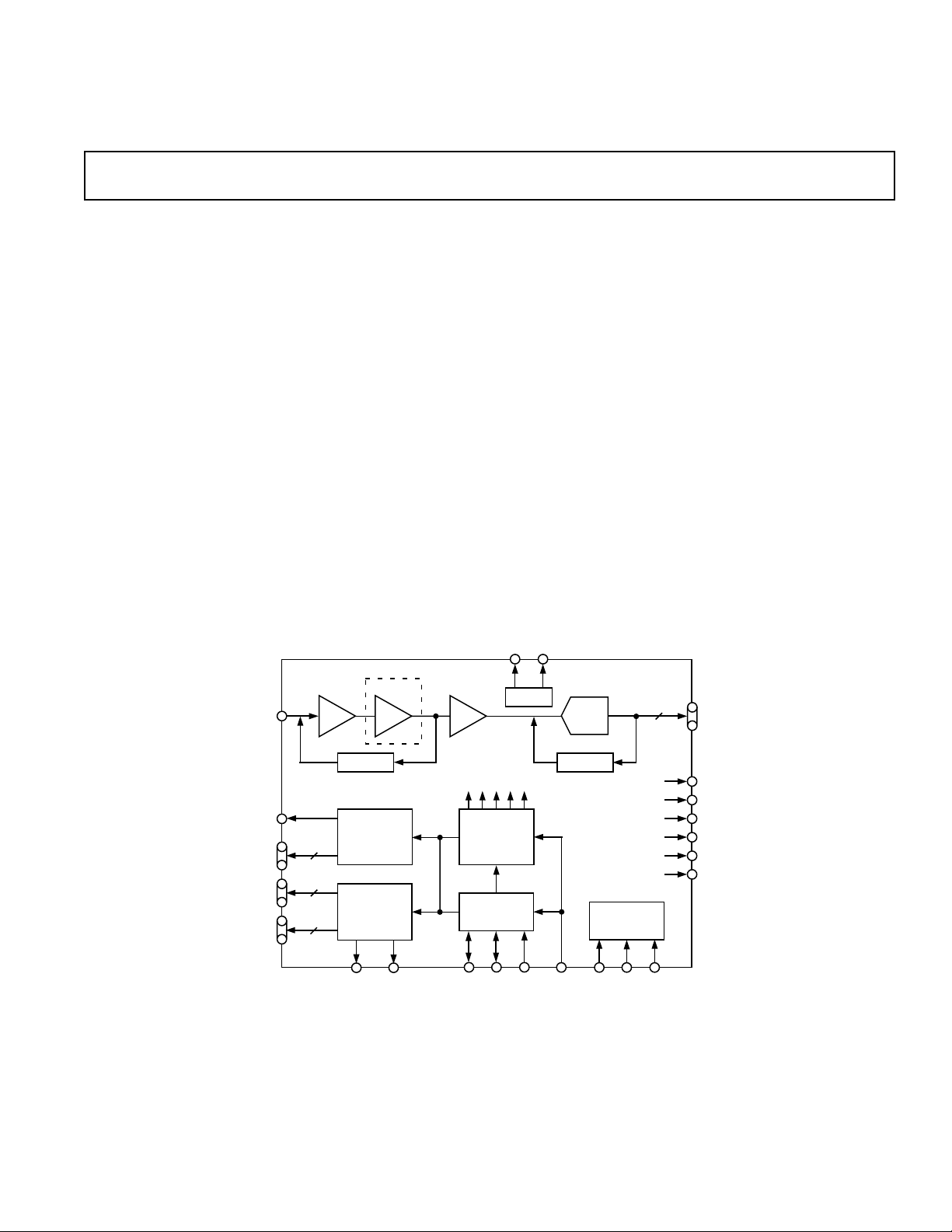
PRODUCT DESCRIPTION
The AD9891 and AD9895 are highly integrated CCD signal
processors for digital still camera applications. Both include a
complete analog front end with A/D conversion combined with
a full-function programmable timing generator. A Precision
Timing core allows adjustment of high speed clocks with 1 ns
resolution at 20 MHz operation and 700 ps resolution at 30
MHz operation.
The AD9891 is specified at pixel rates of up to 20 MHz, and
the AD9895 is specified at 30 MHz. The analog front end
includes black level clamping, CDS, PxGA, VGA, and a 10-Bit
or 12-Bit A/D converter. The timing generator provides all the
necessary CCD clocks: RG, H-clocks, V-clocks, sensor gate
pulses, substrate clock, and substrate bias control. Operation is
programmed using a 3-wire serial interface.
Packaged in a space-saving 64-lead CSPBGA, the AD9891 and
AD9895 are
–20°C to +85°C.
specified over an operating temperature range of
FUNCTIONAL BLOCK DIAGRAM
VRT VRB
4dB 6dB
CCDIN
RG
H1–H4
V1–V4
VSG1–VSG8
PxGA is a registered trademark and Precision Timing is a trademark of Analog Devices, Inc.
4
4
8
PxGACDS
CLAMP
HORIZONTAL
DRIVERS
V- H
CONTROL
VSUB SUBCK HD VD SYNC
2dB TO 36dB
VGA
INTERNAL CLOCKS
PRECISION
TIMING
GENERATOR
SYNC
GENERATOR
VREF
AD9891/AD9895
ADC
CLAMP
REGISTERS
CLI
SL SCK DATA
10 OR 12
DOUT
DCLK
CLPOB/PBLK
FD/LD
MSHUT
STROBE
CLO
INTERNAL
REV. A
Information furnished by Analog Devices is believed to be accurate and
reliable. However, no responsibility is assumed by Analog Devices for its
use, nor for any infringements of patents or other rights of third parties that
may result from its use. No license is granted by implication or otherwise
under any patent or patent rights of Analog Devices.
One Technology Way, P.O. Box 9106, Norwood, MA 02062-9106, U.S.A.
Tel: 781/329-4700 www.analog.com
Fax: 781/326-8703 © Analog Devices, Inc., 2002

AD9891/AD9895
TABLE OF CONTENTS
SPECIFICATIONS . . . . . . . . . . . . . . . . . . . . . . . . . . . . . . . 3
DIGITAL SPECIFICATIONS . . . . . . . . . . . . . . . . . . . . . 3
AD9891 ANALOG SPECIFICATIONS . . . . . . . . . . . . . . 4
AD9895 ANALOG SPECIFICATIONS . . . . . . . . . . . . . . 5
TIMING SPECIFICATIONS . . . . . . . . . . . . . . . . . . . . . . 6
PACKAGE THERMAL CHARACTERISTICS . . . . . . . . 6
ABSOLUTE MAXIMUM RATINGS . . . . . . . . . . . . . . . . . 6
ORDERING GUIDE . . . . . . . . . . . . . . . . . . . . . . . . . . . . . . 6
PIN CONFIGURATION-AD9891 . . . . . . . . . . . . . . . . . . . 7
PIN FUNCTION DESCRIPTIONS-AD9891 . . . . . . . . . . . 7
PIN CONFIGURATION-AD9895 . . . . . . . . . . . . . . . . . . . 8
PIN FUNCTION DESCRIPTIONS-AD9895 . . . . . . . . . . . 8
SPECIFICATION DEFINITIONS . . . . . . . . . . . . . . . . . . . 9
EQUIVALENT CIRCUITS . . . . . . . . . . . . . . . . . . . . . . . . . 9
TYPICAL PERFORMANCE CHARACTERISTICS . . . . 10
SYSTEM OVERVIEW . . . . . . . . . . . . . . . . . . . . . . . . . . . . 11
Typical System Block Diagram . . . . . . . . . . . . . . . . . . . . 11
PRECISION TIMING HIGH SPEED TIMING
GENERATION . . . . . . . . . . . . . . . . . . . . . . . . . . . . . . . . . 12
Timing Resolution . . . . . . . . . . . . . . . . . . . . . . . . . . . . . . .12
High Speed Clock Programmability . . . . . . . . . . . . . . . . . .12
H-Driver and RG Outputs . . . . . . . . . . . . . . . . . . . . . . . . .13
Digital Data Outputs . . . . . . . . . . . . . . . . . . . . . . . . . . . . .13
HORIZONTAL CLAMPING AND BLANKING . . . . . . . . 15
Individual CLPOB, CLPDM, and PBLK Sequences . . . . .15
Individual HBLK Sequences . . . . . . . . . . . . . . . . . . . . . . .15
Horizontal Sequence Control . . . . . . . . . . . . . . . . . . . . . . .15
VERTICAL TIMING GENERATION . . . . . . . . . . . . . . . .17
Individual Vertical Sequences . . . . . . . . . . . . . . . . . . . . . .18
Individual Vertical Regions . . . . . . . . . . . . . . . . . . . . . . . .19
Complete Field: Combining the Regions . . . . . . . . . . . . . .20
Vertical Sequence Alteration . . . . . . . . . . . . . . . . . . . . . . .21
Second Vertical Sequence During VSG Lines . . . . . . . . . .22
Vertical Sweep Mode Operation . . . . . . . . . . . . . . . . . . . .22
Vertical Multiplier Mode . . . . . . . . . . . . . . . . . . . . . . . . . .24
Frame Transfer CCD Mode . . . . . . . . . . . . . . . . . . . . . . 24
Vertical Sensor Gate (Shift Gate) Timing . . . . . . . . . . . . .25
SHUTTER TIMING CONTROL . . . . . . . . . . . . . . . . . . . .26
Normal Shutter Mode . . . . . . . . . . . . . . . . . . . . . . . . . . . .26
High Precision Shutter Mode . . . . . . . . . . . . . . . . . . . . . . .26
Low Speed Shutter Mode . . . . . . . . . . . . . . . . . . . . . . . . .26
SUBCK Suppression . . . . . . . . . . . . . . . . . . . . . . . . . . . . .26
Readout After Exposure . . . . . . . . . . . . . . . . . . . . . . . . . . .27
VSUB Control . . . . . . . . . . . . . . . . . . . . . . . . . . . . . . . . . .27
MSHUT and STROBE Control . . . . . . . . . . . . . . . . . . . .27
Example of Exposure and Readout of Interlaced Frame . . .29
ANALOG FRONT END DESCRIPTION AND
OPERATION . . . . . . . . . . . . . . . . . . . . . . . . . . . . . . . . . . . 30
DC Restore . . . . . . . . . . . . . . . . . . . . . . . . . . . . . . . . . . . 30
Correlated Double Sampler . . . . . . . . . . . . . . . . . . . . . . . 30
Input Clamp . . . . . . . . . . . . . . . . . . . . . . . . . . . . . . . . . . 30
PxGA . . . . . . . . . . . . . . . . . . . . . . . . . . . . . . . . . . . . . . . 30
PxGA Color Steering Mode Timing . . . . . . . . . . . . . . . . 31
Variable Gain Amplifier . . . . . . . . . . . . . . . . . . . . . . . . . . 33
PxGA and VGA Gain Curves . . . . . . . . . . . . . . . . . . . . . 33
Optical Black Clamp . . . . . . . . . . . . . . . . . . . . . . . . . . . . 33
A/D Converter . . . . . . . . . . . . . . . . . . . . . . . . . . . . . . . . . 33
POWER-UP AND SYNCHRONIZATION . . . . . . . . . . . . 34
Recommended Power-Up Sequence for Master Mode . . . .34
SYNC During Master Mode Operation . . . . . . . . . . . . . . .35
Synchronization in Slave Mode . . . . . . . . . . . . . . . . . . . . .35
POWER-DOWN MODE OPERATION . . . . . . . . . . . . . . 35
HORIZONTAL TIMING SEQUENCE EXAMPLE . . . . . 37
VERTICAL TIMING EXAMPLE . . . . . . . . . . . . . . . . . . . 39
CIRCUIT LAYOUT INFORMATION . . . . . . . . . . . . . . . .40
SERIAL INTERFACE TIMING . . . . . . . . . . . . . . . . . . . . .41
Notes About Accessing a Double-Wide Register . . . . . . . 41
NOTES ON REGISTER LISTING . . . . . . . . . . . . . . . . . . 42
COMPLETE REGISTER LISTING . . . . . . . . . . . . . . . . . 43
OUTLINE DIMENSIONS . . . . . . . . . . . . . . . . . . . . . . . . . 57
REVISION HISTORY . . . . . . . . . . . . . . . . . . . . . . . . . . . . 57
REV. A–2–

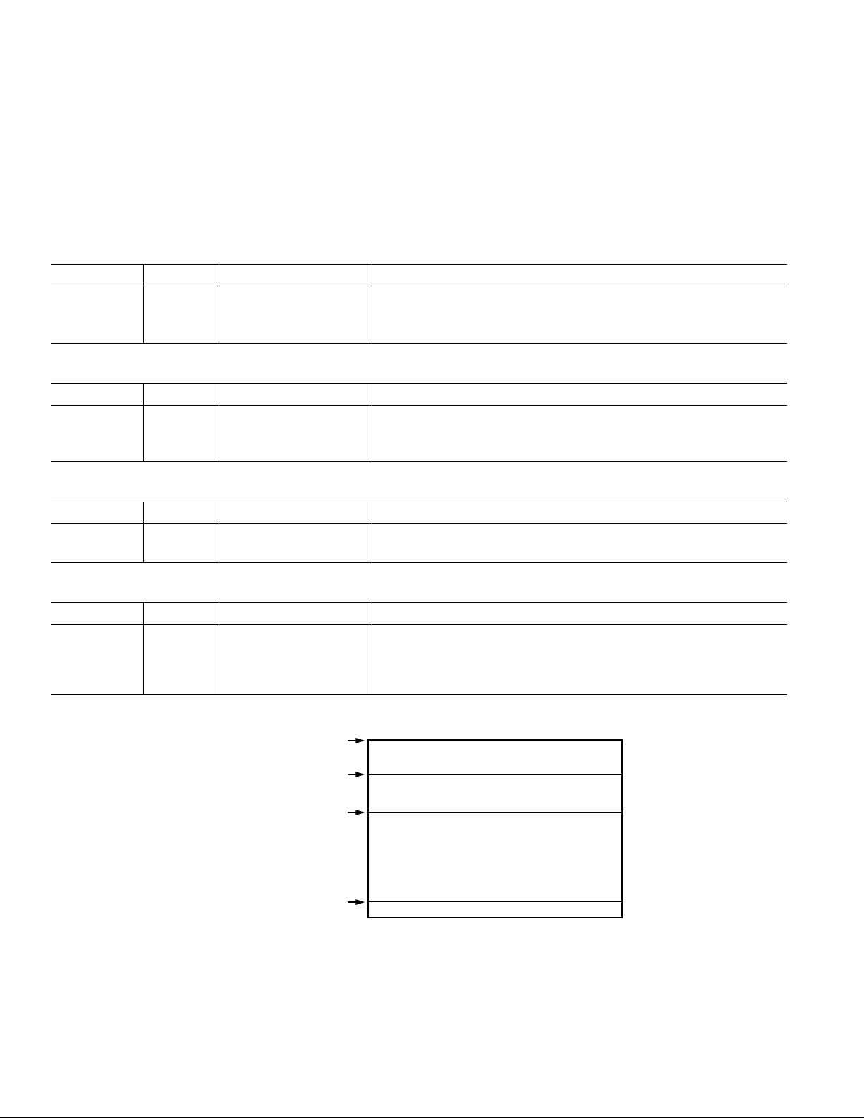
AD9891/AD9895–SPECIFICATIONS
Parameter Min Typ Max Unit
TEMPERATURE RANGE
Operating –20 +85 °C
Storage –65 +150 °C
POWER SUPPLY VOLTAGE
AVDD1, AVDD2 (AFE Analog Supply) 2.7 3.0 3.6 V
TCVDD (Timing Core Analog Supply) 2.7 3.0 3.6 V
RGVDD (RG Driver) 3.0 5.0 5.25 V
HVDD (H1–H4 Drivers) 3.0 5.0 5.25 V
DRVDD (Data Output Drivers) 2.7 3.0 3.6 V
DVDD (Digital) 2.7 3.0 3.6 V
POWER DISSIPATION–AD9891 (See TPC 1 for Power Curves)
20 MHz, Typ Supply Levels, 100 pF H1–H4 Loading 380 mW
Power from HVDD Only
Power-Down 1 Mode 42 mW
Power-Down 2 Mode 8 mW
Power-Down 3 Mode 2.5 mW
POWER DISSIPATION–AD9895 (See TPC 4 for Power Curves)
30 MHz, Typ Supply Levels, 100 pF H1–H4 Loading 600 mW
Power from HVDD Only
Power-Down 1 Mode 138 mW
Power-Down 2 Mode 22 mW
Power-Down 3 Mode 2.5 mW
MAXIMUM CLOCK RATE (CLI)
AD9891 20 MHz
AD9895 30 MHz
*
The total power dissipated by the HVDD supply may be approximated using the equation:
Total HVDD Power = [C
Reducing the H-loading, using only two of the outputs, and/or using a lower HVDD supply will reduce the power dissipation.
Actual HVDD power may be slightly higher than the calculated value because of stray capacitance inherent in the PCB layout/routing.
Specifications subject to change without notice.
*
*
HVDD Pixel Frequency]
LOAD
HVDD
Number of H-Outputs Used
220 mW
320 mW
DIGITAL SPECIFICATIONS
(RGVDD = HVDD = 4.75 V to 5.25 V, DVDD = DRVDD = 2.7 V to 3.5 V, CL = 20 pF, T
unless otherwise noted.)
MIN
to T
MAX
Parameter Symbol Min Typ Max Unit
LOGIC INPUTS
High Level Input Voltage V
Low Level Input Voltage V
High Level Input Current I
Low Level Input Current I
Input Capacitance C
IH
IL
IH
IL
IN
2.1 V
0.6 V
10 µA
10 µA
10 pF
LOGIC OUTPUTS (Except H and RG)
High Level Output Voltage @ IOH = 2 mA V
Low Level Output Voltage @ IOL = 2 mA V
OH
OL
2.2 V
0.5 V
RG and H-DRIVER OUTPUTS (H1–H4)
High Level Output Voltage @ Max Current V
Low Level Output Voltage @ Max Current V
OH
OL
VDD – 0.5 V
0.5 V
Maximum Output Current (Programmable) 24 mA
Maximum Load Capacitance (for Each Output) 100 pF
Specifications subject to change without notice.
,
REV. A –3–
AD9891/AD9895
AD9891–ANALOG SPECIFICATIONS
(AVDD1, AVDD2 = 3.0 V, f
= 20 MHz, T
CLI
MIN
to T
, unless otherwise noted.)
MAX
Parameter Min Typ Max Unit Notes
CDS
Gain 0 dB
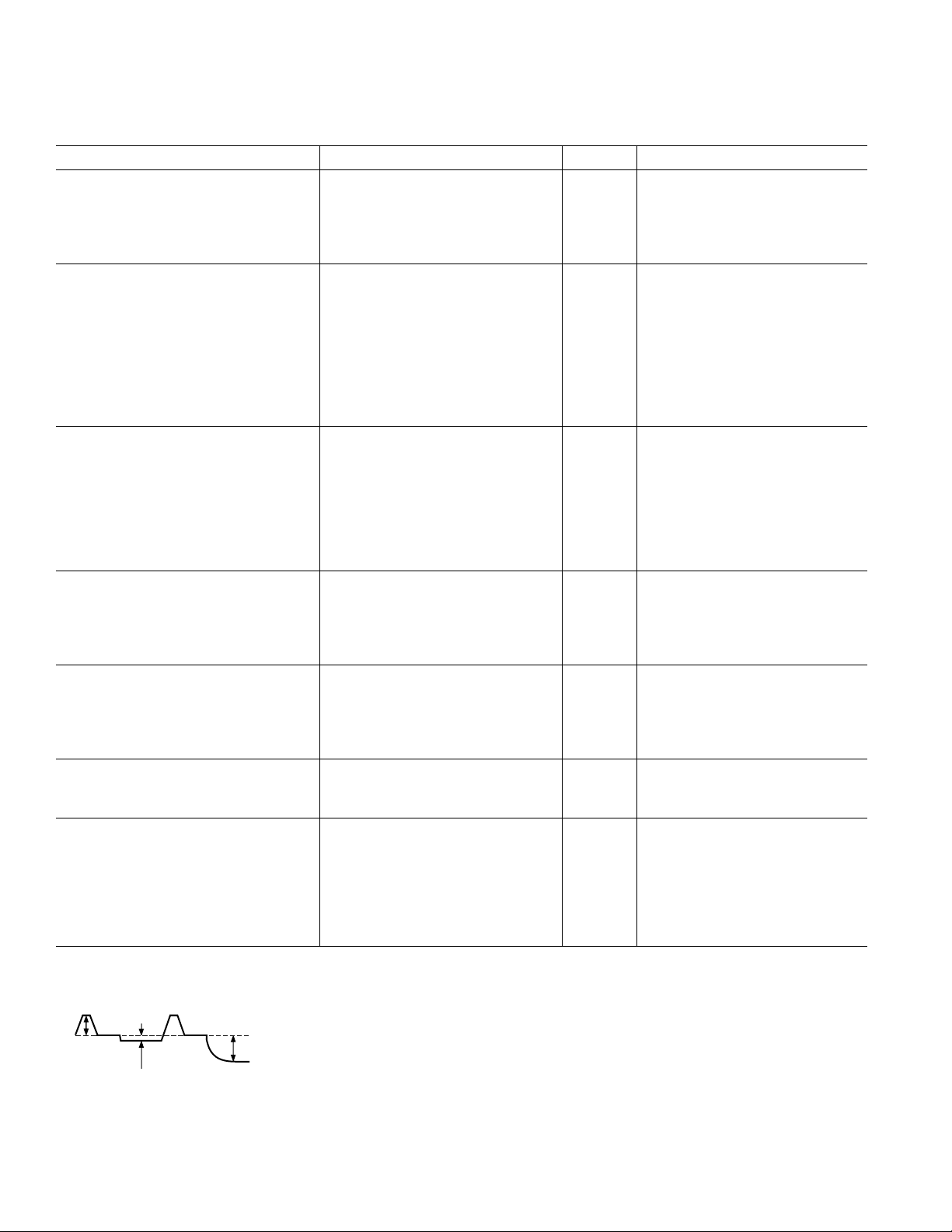
Allowable CCD Reset Transient 500 mV Input signal characteristics*
Max Input Range before Saturation 1.0 V p-p
Max CCD Black Pixel Amplitude ± 200 mV
PIXEL GAIN AMPLIFIER (PxGA)
Max Input Range 1.0 V p-p
Max Output Range 1.6 V p-p
Gain Control Resolution 64 Steps
Gain Monotonicity Guaranteed
Gain Range
Min Gain (PxGA Code 32) –2.5 dB
Med Gain (PxGA Code 0) +3.5 dB Default setting
Max Gain (PxGA Code 31) +9.5 dB
VARIABLE GAIN AMPLIFIER (VGA)
Max Input Range 1.6 V p-p
Max Output Range 2.0 V p-p
Gain Control Resolution 1024 Steps
Gain Monotonicity Guaranteed
Gain Range
Low Gain (VGA Code 70) 2 dB
Max Gain (VGA Code 1023) 36 dB
BLACK LEVEL CLAMP
Clamp Level Resolution 256 Steps
Clamp Level Measured at ADC output
Min Clamp Level 0 LSB
Max Clamp Level 63.75 LSB
A/D CONVERTER
Resolution 10 Bits
Differential Nonlinearity (DNL) ± 0.4 ± 1.0 LSB
No Missing Codes Guaranteed
Full-Scale Input Voltage 2.0 V
VOLTAGE REFERENCE
Reference Top Voltage (VRT) 2.0 V
Reference Bottom Voltage (VRB) 1.0 V
SYSTEM PERFORMANCE Includes entire signal chain
Gain Accuracy Includes 4 dB default PxGA gain
Low Gain (VGA Code 70) 5 6 7 dB Gain = (0.035 Code) + 3.55 dB
Max Gain (VGA Code 1023) 38.5 39.5 40.5 dB
Peak Nonlinearity, 500 mV Input Signal 0.2 % 12 dB gain applied
Total Output Noise 0.6 LSB rms AC grounded input, 6 dB gain applied
Power Supply Rejection (PSR) 40 dB Measured with step change on supply
*
Input signal characteristics defined as follows:
500mV TYP
RESET
TRANSIENT
200mV MAX
OPTICAL
BLACK PIXEL
Specifications subject to change without notice.
1V MAX
INPUT
SIGNAL RANGE
REV. A–4–
AD9891/AD9895
AD9895–ANALOG SPECIFICATIONS
(AVDD1, AVDD2 = 3.0 V, f
= 30 MHz, T
CLI
MIN
to T
, unless otherwise noted.)
MAX
Parameter Min Typ Max Unit Notes
CDS
Gain 0 dB
Allowable CCD Reset Transient 500 mV Input signal characteristics*
Max Input Range before Saturation 1.0 V p-p
Max CCD Black Pixel Amplitude ± 200 mV
PIXEL GAIN AMPLIFIER (PxGA)
Max Input Range 1.0 V p-p
Max Output Range 1.6 V p-p
Gain Control Resolution 64 Steps
Gain Monotonicity Guaranteed
Gain Range
Min Gain (PxGA Code 32) –2.5 dB
Med Gain (PxGA Code 0) +3.5 dB Default setting
Max Gain (PxGA Code 31) +9.5 dB
VARIABLE GAIN AMPLIFIER (VGA)
Max Input Range 1.6 V p-p
Max Output Range 2.0 V p-p
Gain Control Resolution 1024 Steps
Gain Monotonicity Guaranteed
Gain Range
Low Gain (VGA Code 70) 2 dB
Max Gain (VGA Code 1023) 36 dB
BLACK LEVEL CLAMP
Clamp Level Resolution 256 Steps
Clamp Level Measured at ADC output
Min Clamp Level 0 LSB
Max Clamp Level 255 LSB
A/D CONVERTER
Resolution 12 Bits
Differential Nonlinearity (DNL) ± 0.5 ± 1.0 LSB
No Missing Codes Guaranteed
Full-Scale Input Voltage 2.0 V
VOLTAGE REFERENCE
Reference Top Voltage (VRT) 2.0 V
Reference Bottom Voltage (VRB) 1.0 V
SYSTEM PERFORMANCE Includes entire signal chain
Gain Accuracy Includes 4 dB default PxGA gain
Low Gain (VGA Code 70) 5 6 7 dB Gain = (0.035 Code) + 3.55 dB
Max Gain (VGA Code 1023) 38.5 39.5 40.5 dB
Peak Nonlinearity, 500 mV Input Signal 0.2 % 12 dB gain applied
Total Output Noise 0.8 LSB rms AC grounded input, 6 dB gain applied
Power Supply Rejection (PSR) 40 dB Measured with step change on supply
*
Input signal characteristics defined as follows:
500mV TYP
RESET
TRANSIENT
200mV MAX
OPTICAL
BLACK PIXEL
Specifications subject to change without notice.
1V MAX
INPUT
SIGNAL RANGE
REV. A
–5–
AD9891/AD9895
WARNING!
ESD SENSITIVE DEVICE
TIMING SPECIFICATIONS
(CL = 20 pF, AVDD = DVDD = DRVDD = 3.0 V, f
otherwise noted.)
= 20 MHz [AD9891] or 30 MHz [AD9895], unless
CLI
Parameter Symbol Min Typ Max Unit
MASTER CLOCK, CLI (Figure 7)
CLI Clock Period, AD9891 t
CONV
50 ns
CLI High/Low Pulsewidth, AD9891 20 25 ns
CLI Clock Period, AD9895 t
CONV
33.3 ns
CLI High/Low Pulsewidth, AD9895 13 16.7 ns
Delay from CLI Rising Edge to Internal Pixel Position 0 t
1
AFE CLAMP PULSES
CLPDM Pulsewidth 410Pixels
CLPOB Pulsewidth
AFE SAMPLE LOCATION
(Figure 13)
2
1
(Figure 10)
SHP Sample Edge to SHD Sample Edge, AD9891 t
SHP Sample Edge to SHD Sample Edge, AD9895 t
DATA OUTPUTS (Figure 12)
Output Delay from DCLK Rising Edge
1
CLIDLY
S1
S1
t
OD
220Pixels
20 25 ns
13 16.7 ns
6ns
8ns
Pipeline Delay from SHP/SHD Sampling 9 Cycles
SERIAL INTERFACE (Figures 52 and 53)
Maximum SCK Frequency f
SL to SCK Setup Time t
SCK to SL Hold Time t
SDATA Valid to SCK Rising Edge Setup t
SCK Falling Edge to SDATA Valid Hold t
SCK Falling Edge to SDATA Valid Read t
NOTES
1
Parameter is programmable.
2
Minimum CLPOB pulsewidth is for functional operation only. Wider typical pulses are recommended to achieve good clamp performance.
SCLK
LS
LH
DS
DH
DV
10 MHz
10 ns
10 ns
10 ns
10 ns
10 ns
ABSOLUTE MAXIMUM RATINGS
With
Respect
Parameter To Min Max Unit
AVDD1, AVDD2 AVSS –0.3 +3.9 V
PACKAGE THERMAL CHARACTERISTICS
Thermal Resistance
JA = 61°C/W
= 29.7°C/W
JC
ORDERING GUIDE
TCVDD TCVSS –0.3 +3.9 V
HVDD HVSS –0.3 +5.5 V
RGVDD RGVSS –0.3 +5.5 V
DVDD DVSS –0.3 +3.9 V
DRVDD DRVSS –0.3 +3.9 V
RG Output RGVSS –0.3 RGVDD + 0.3 V
Model Range Description Option
AD9891KBC –20°C to +85°C CSPBGA BC-64
AD9895KBC –20°C to +85°C CSPBGA BC-64
Temperature Package Package
H1–H4 Output HVSS –0.3 HVDD + 0.3 V
Digital Outputs DVSS –0.3 DVDD + 0.3 V
Digital Inputs DVSS –0.3 DVDD + 0.3 V
SCK, SL, SDATA DVSS –0.3 DVDD + 0.3 V
VRT, VRB AVSS –0.3 AVDD + 0.3 V
BYP1–BYP3, CCDIN AVSS –0.3 AVDD + 0.3 V
Junction Temperature 150 °C
Lead Temperature, 10 sec 350 °C
CAUTION
ESD (electrostatic discharge) sensitive device. Electrostatic charges as high as 4000 V readily
accumulate on the human body and test equipment and can discharge without detection. Although the
AD9891 and AD9895 feature proprietary ESD protection circuitry, permanent damage may occur on
devices subjected to high energy electrostatic discharges. Therefore, proper ESD precautions are
recommended to avoid performance degradation or loss of functionality.
REV. A–6–
AD9891 PIN CONFIGURATION
A1 CORNER
INDEX AREA
1234567 9108
A
B
C
AD9891
TOP
VIEW
(Not to Scale)
D
E
F
G
H
J
K
AD9891/AD9895
PIN FUNCTION DESCRIPTIONS
Pin Mnemonic Type2Description
A1 VD DO Vertical Sync Pulse
(Input for Slave Mode,
Output for Master Mode)
B1 HD DO Horizontal Sync Pulse
(Input for Slave Mode,
Output for Master Mode)
C1 SYNCDIExternal System Sync Input
C2 LD/FD DO Line or Field Designator
Output
D1 DCLK DO Data Clock Output
D2 CLPOB/ DO CLPOB or PBLK Output
PBLK
E1 NC Not Internally Connected
E2 NC Not Internally Connected
F2 DO/SDO DO Data Output (LSB)
(also Serial Data Output
3
)
F1 D1 DO Data Output
G2 D2 DO Data Output
G1 D3 DO Data Output
H2 D4 DO Data Output
H1 D5 DO Data Output
J2 D6 DO Data Output
J1 D7 DO Data Output
K2 D8 DO Data Output
K1 D9 DO Data Output (MSB)
K3 DRVDD P Data Output Driver Supply
K4 DRVSS P Data Output Driver Ground
J3 VSUB DO CCD Substrate Bias
J4 SUBCK DO CCD Substrate Clock
(E-Shutter)
K5 V1 DO CCD Vertical Transfer Clock 1
J5 V2 DO CCD Vertical Transfer Clock 2
K6 V3 DO CCD Vertical Transfer Clock 3
J6 V4 DO CCD Vertical Transfer Clock 4
K7 VSG1/V5DO CCD Sensor Gate Pulse 1
(also V5
J7 VSG2/V6DO CCD Sensor Gate Pulse 2
(also V6
K8 VSG3/V7DO CCD Sensor Gate Pulse 3
(also V7
4
)
4
)
4
)
J8 VSG4/V8DO CCD Sensor Gate Pulse 4
(also V84)
1
Pin Mnemonic Type2Description
K9 VSG5 DO CCD Sensor Gate Pulse 5
J9 VSG6DOCCD Sensor Gate Pulse 6
K10 VSG7DOCCD Sensor Gate Pulse 7
J10 VSG8 DO CCD Sensor Gate Pulse 8
H10 H1 DO CCD Horizontal Clock 1
H9 H2 DO CCD Horizontal Clock 2
G10 HVDD P H1–H4 Driver Supply
G9 HVSS P H1–H4 Driver Ground
F10 H3 DO CCD Horizontal Clock 3
F9 H4 DO CCD Horizontal Clock 4
E10 RGVDD P RG Driver Supply
E9 RGVSS P RG Driver Ground
D9 RG DO CCD Reset Gate Clock
D10 CLO DO Reference Clock Output for
Crystal
C10 CLI DI Reference Clock Input
B10 TCVDD P Analog Supply for Timing Core
C9 TCVSS P Analog Ground for Timing
Core
A10 AVDD1 P Analog Supply for AFE
B9 AVSS1 P Analog Ground for AFE
A9 BYP1 AO Analog Circuit Bypass
B8 BYP2 AO Analog Circuit Bypass
A8 CCDIN AI CCD Signal Input
A7 BYP3 AO Analog Circuit Bypass
B7 AVDD2 P Analog Supply for AFE
B6 AVSS2 P Analog Ground for AFE
A6 REFB AO Voltage Reference Bottom
Bypass
A5 REFT AO Voltage Reference Top Bypass
B5 SL DI 3-Wire Serial Load Pulse
A4 SDI DI 3-Wire Serial Data Input
B4 SCK DI 3-Wire Serial Clock
A3 MSHUT DO Mechanical Shutter Pulse
B3 STROBE DO Strobe Pulse
B2 DVSS P Digital Ground
A2 DVDD P Digital Supply for VSG,
V1–V4, HD, VD, MSHUT,
STROBE, and Serial Interface
NOTES
1
See Figure 50 for circuit configuration.
2
AI = Analog Input, AO = Analog Output, DI = Digital Input,
DO = Digital Output, DIO = Digital Input/Output, P = Power.
3
In Register Readback Mode
4
In Frame Transfer CCD Mode
REV. A
–7–
AD9891/AD9895
AD9895 PIN CONFIGURATION
A1 CORNER
INDEX AREA
1234567 9108
A
B
C
AD9895
TOP
VIEW
(Not to Scale)
D
E
F
G
H
J
K
PIN FUNCTION DESCRIPTIONS
Pin Mnemonic Type2Description
A1 VD DO Vertical Sync Pulse
(Input for Slave Mode,
Output for Master Mode)
B1 HD DO Horizontal Sync Pulse
(Input for Slave Mode,
Output for Master Mode)
C1 SYNCDIExternal System Sync Input
C2 LD/FD DO Line or Field Designator
Output
D1 DCLK DO Data Clock Output
D2 CLPOB/ DO CLPOB or PBLK Output
PBLK
E2 DO DO Data Output (LSB)
E1 D1 DO Data Output
F2 D2/SDO DO Data Output
(also Serial Data Output
3
)
F1 D3 DO Data Output
G2 D4 DO Data Output
G1 D5 DO Data Output
H2 D6 DO Data Output
H1 D7 DO Data Output
J2 D8 DO Data Output
J1 D9 DO Data Output
K2 D10 DO Data Output
K1 D11 DO Data Output (MSB)
K3 DRVDD P Data Output Driver Supply
K4 DRVSS P Data Output Driver Ground
J3 VSUB DO CCD Substrate Bias
J4 SUBCK DO CCD Substrate Clock
(E-Shutter)
K5 V1 DO CCD Vertical Transfer Clock 1
J5 V2 DO CCD Vertical Transfer Clock 2
K6 V3 DO CCD Vertical Transfer Clock 3
J6 V4 DO CCD Vertical Transfer Clock 4
K7 VSG1/V5DO CCD Sensor Gate Pulse 1
(also V5
J7 VSG2/V6DO CCD Sensor Gate Pulse 2
(also V6
K8 VSG3/V7DO CCD Sensor Gate Pulse 3
(also V7
4
)
4
)
4
)
J8 VSG4/V8DO CCD Sensor Gate Pulse 4
(also V84)
1
Pin Mnemonic Type2Description
K9 VSG5 DO CCD Sensor Gate Pulse 5
J9 VSG6DOCCD Sensor Gate Pulse 6
K10 VSG7DOCCD Sensor Gate Pulse 7
J10 VSG8 DO CCD Sensor Gate Pulse 8
H10 H1 DO CCD Horizontal Clock 1
H9 H2 DO CCD Horizontal Clock 2
G10 HVDD P H1–H4 Driver Supply
G9 HVSS P H1–H4 Driver Ground
F10 H3 DO CCD Horizontal Clock 3
F9 H4 DO CCD Horizontal Clock 4
E10 RGVDD P RG Driver Supply
E9 RGVSS P RG Driver Ground
D9 RG DO CCD Reset Gate Clock
D10 CLO DO Reference Clock Output for
Crystal
C10 CLI DI Reference Clock Input
B10 TCVDD P Analog Supply for Timing Core
C9 TCVSS P Analog Ground for Timing
Core
A10 AVDD1 P Analog Supply for AFE
B9 AVSS1 P Analog Ground for AFE
A9 BYP1 AO Analog Circuit Bypass
B8 BYP2 AO Analog Circuit Bypass
A8 CCDIN AI CCD Signal Input
A7 BYP3 AO Analog Circuit Bypass
B7 AVDD2 P Analog Supply for AFE
B6 AVSS2 P Analog Ground for AFE
A6 REFB AO Voltage Reference Bottom
Bypass
A5 REFT AO Voltage Reference Top Bypass
B5 SL DI 3-Wire Serial Load Pulse
A4 SDI DI 3-Wire Serial Data Input
B4 SCK DI 3-Wire Serial Clock
A3 MSHUT DO Mechanical Shutter Pulse
B3 STROBE DO Strobe Pulse
B2 DVSS P Digital Ground
A2 DVDD P Digital Supply for VSG,
V1–V4, HD, VD, MSHUT,
STROBE, and Serial Interface
NOTES
1
See Figure 50 for circuit configuration.
2
AI = Analog Input, AO = Analog Output, DI = Digital Input,
DO = Digital Output, DIO = Digital Input/Output, P = Power.
3
In Register Readback Mode
4
In Frame Transfer CCD Mode
REV. A–8–
AD9891/AD9895
SPECIFICATION DEFINITIONS
Differential Nonlinearity (DNL)
An ideal ADC exhibits code transitions that are exactly 1 LSB
apart. DNL is the deviation from this ideal value. Thus, every
code must have a finite width. No missing codes guaranteed to
12-bit resolution indicates that all 4096 codes, respectively,
must be present over all operating conditions.
Peak Nonlinearity
Peak nonlinearity, a full signal chain specification, refers to the
peak deviation of the output of the AD9891/AD9895 from a
true straight line. The point used as “zero scale” occurs 0.5 LSB
before the first code transition. “Positive full scale” is defined as
a level 1 and 0.5 LSB beyond the last code transition. The
deviation is measured from the middle of each particular output
code to the true straight line. The error is then expressed as a
EQUIVALENT CIRCUITS
AV DD1
R
percentage of the 2 V ADC full-scale signal. The input signal is
always appropriately gained up to fill the ADC’s full-scale range.
Total Output Noise
The rms output noise is measured using histogram techniques. The
standard deviation of the ADC output codes is calculated in LSB
and represents the rms noise level of the total signal chain at the
specified gain setting. The output noise can be converted to an
equivalent voltage, using the relationship 1 LSB = (ADC Full
n
Scale/2
codes) when n is the bit resolution of the ADC. For the
AD9891, 1 LSB is 2 mV, while for the AD9895, 1 LSB is 0.5 mV.
Power Supply Rejection (PSR)
The PSR is measured with a step change applied to the supply
pins. The PSR specification is calculated from the change in the
data outputs for a given step change in the supply voltage.
DVD D
330
DATA
THREE-
STATE
AVSS1 AVSS1
Figure 1. CCDIN
DVD D
DVSS
Figure 2. Digital Data Outputs
DRVDD
DRVSS
DOUT
RG, H1–H4
ENABLE
DVSS
Figure 3. Digital Inputs
HVDD OR
RGVDD
HVSS OR
RGVSS
Figure 4. H1–H4, RG Drivers
OUTPUT
REV. A
–9–
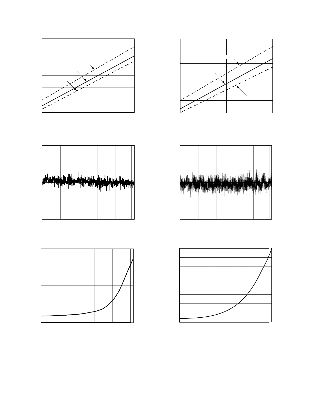
AD9891/AD9895–Typical Performance Characteristics
440
RGVDD = HVDD = 5.0V
400
360
320
280
POWER DISSIPATION – mW
240
200
10
VDD = 2.7V
VDD = 3.3V
VDD = 3.0V
15
SAMPLE RATE – MHz
TPC 1. AD9891 Power vs. Sample Rate
1.0
0.5
0
725
RGVDD = HVDD = 5.0V
650
VDD = 3.3V
575
VDD = 3.0V
500
425
POWER DISSIPATION – mW
350
20
275
10
20
SAMPLE RATE – MHz
VDD = 2.7V
30
TPC 4. AD9895 Power vs. Sample Rate
1.0
0.5
0
–0.5
–1.0
0
200 600 800
400
TPC 2. AD9891 Typical DNL Performance
4
3
2
OUTPUT NOISE – LSB
1
0
0
200
400
VGA GAIN CODE – LSB
600
800
TPC 3. AD9891 Output Noise vs. VGA Gain
1000
1000
–0.5
–1.0
0
800 2400 3200
1600
TPC 5. AD9895 Typical DNL Performance
24
21
18
15
12
9
OUTPUT NOISE – LSB
6
3
0
0
200
400
VGA GAIN CODE – LSB
600
800
TPC 6. AD9895 Output Noise vs. VGA Gain
4000
1000
REV. A–10–
AD9891/AD9895
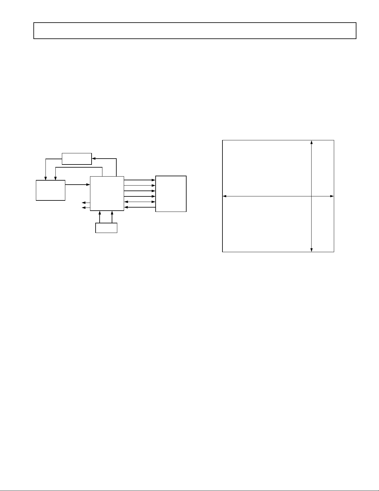
SYSTEM OVERVIEW
Figure 5 shows the typical system block diagram for the AD9891/
AD9895 used in Master Mode. The CCD output is processed by
the AD9891/AD9895’s AFE circuitry, which consists of a CDS,
PxGA, VGA, black level clamp, and an A/D converter. The digitized pixel information is sent to the digital image processor chip,
which performs the post-processing and compression. To operate
the CCD, all CCD timing parameters are programmed into the
AD9891/AD9895 from the system microprocessor, through the
3-wire serial interface. From the system master clock, CLI, provided by the image processor or external crystal, the AD9891/
AD9895 generates all of the CCD’s horizontal and vertical clocks
and all internal AFE clocks. External synchronization is provided
by a SYNC pulse from the microprocessor, which will reset
internal counters and resync the VD and HD outputs.
V- DRIVER
H1–H4, RG, VSUB
CCDIN
CCD
MSHUT
STROBE
V1–V4, VSG1–VSG8, SUBCK
AD989x
SERIAL
INTERFACE
P
SYNC
DOUT
DCLK
CLPOB/PBLK
LD/FD
HD, VD
CLI
DIGITAL
IMAGE
PROCESSING
ASIC
Figure 5. Typical System Block Diagram, Master Mode
Alternatively, the AD9891/AD9895 may be operated in Slave
Mode, in which the VD and HD are provided externally from
the image processor. In this mode, all AD9891/AD9895 timing
will be synchronized with VD and HD.
The H-drivers for H1–H4 and RG are included in the AD9891/
AD9895, allowing these clocks to be directly connected to the CCD.
H-drive voltage of up to 5 V is supported. An external V-driver is
required for the vertical transfer clocks, the sensor gate pulses,
and the substrate clock.
The AD9891/AD9895 also includes programmable MSHUT
and STROBE outputs, which may be used to trigger mechanical shutter and strobe (flash) circuitry.
Figure 6 shows the horizontal and vertical counter dimensions
for the AD9891/AD9895. All internal horizontal and vertical
clocking is programmed using these dimensions to specify line
and pixel locations.
MAXIMUM
FIELD
DIMENSIONS
12-BIT HORIZONTAL = 4096 PIXELS MAX
12-BIT VERTICAL = 4096 LINES MAX
Figure 6. Vertical and Horizontal Counters
REV. A
–11–
AD9891/AD9895
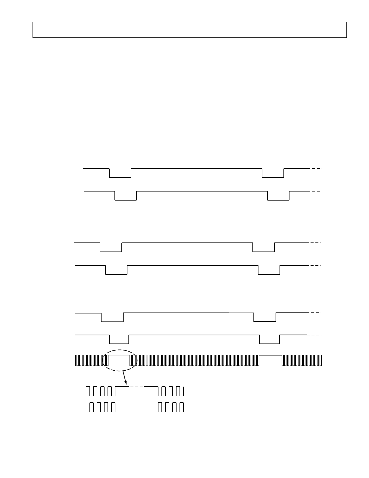
PRECISION TIMING HIGH SPEED TIMING GENERATION
The AD9891/AD9895 generates flexible, high speed timing
signals using the Precision Timing core. This core is the foundation for generating the timing used for both the CCD and the
AFE: the reset gate RG, horizontal drivers H1–H4, and the
SHP/SHD sample clocks. A unique architecture makes it routine for the system designer to optimize image quality by
providing precise control over the horizontal CCD readout and
the AFE correlated double sampling.
The high speed timing of the AD9891/AD9895 operates the
same in either Master or Slave Mode configuration.
Timing Resolution
The Precision Timing core uses a 1 master clock input (CLI) as
a reference. This clock should be the same as the CCD pixel
clock frequency. Figure 7 illustrates how the internal timing
core divides the master clock period into 48 steps or edge positions. Using a 20 MHz CLI frequency, the edge resolution of
the Precision Timing core is 1 ns. If a 1 system clock is not
available, it is also possible to use a 2 reference clock by programming the CLIDIVIDE Register (Addr x01F). The AD9891/
AD9895 will then internally divide the CLI frequency by two.
POSITION
CLI
P[0] P[48] = P[0]P[12] P[24] P[36]
The AD9891/AD9895 also includes a master clock output,
CLO, which is the inverse of CLI. This output is intended to be
used as a crystal driver. A crystal can be placed between the
CLI and CLO Pins to generate the master clock for the
AD9891/AD9895. For more information on using a crystal, see
Figure 51.
High Speed Clock Programmability
Figure 8 shows how the high speed clocks RG, H1–H4, SHP,
and SHD are generated. The RG pulse has programmable
rising
and falling edges, and may be inverted using the polarity
control.
The horizontal clocks H1 and H3 have programmable
rising and falling edges and polarity control. The H2 and H4
clocks are always inverses of H1 and H3, respectively.
Table I summarizes the high speed timing registers and their
parameters. Figure 9 shows the typical 2-phase H-clock
arrangement in which H3 and H4 are programmed for the same
edge location as H1 and H2.
The edge location registers are six bits wide, but there are only
48 valid edge locations available. Therefore, the register values
are mapped into four quadrants, with each quadrant containing
12 edge locations. Table II shows the correct register values for
t
CLIDLY
1 PIXEL
PERIOD
NOTES
PIXEL CLOCK PERIOD IS DIVIDED INTO 48 POSITIONS, PROVIDING FINE EDGE RESOLUTION FOR HIGH SPEED CLOCKS.
THERE IS A FIXED DELAY FROM THE CLI INPUT TO THE INTERNAL PIXEL PERIOD POSITIONS (
t
CLIDLY
= 6ns TYP).
Figure 7. High Speed Clock Resolution from CLI Master Clock Input
3
CCD
SIGNAL
12
RG
56
H1
H2
78
H3
H4
4
PROGRAMMABLE CLOCK POSITIONS:
1: RG RISING EDGE
2: RG FALLING EDGE
3: SHP SAMPLE LOCATION
4: SHD SAMPLE LOCATION
5: H1 RISING EDGE POSITION AND 6: H1 FALLING EDGE POSITION (H2 IS INVERSE OF H1)
7: H3 RISING EDGE POSITION AND 8: H3 FALLING EDGE POSITION (H4 IS INVERSE OF H3)
Figure 8. High Speed Clock Programmable Locations
REV. A–12–
AD9891/AD9895
the corresponding edge locations. Figure 10 shows the range
and default locations of the high speed clock signals.
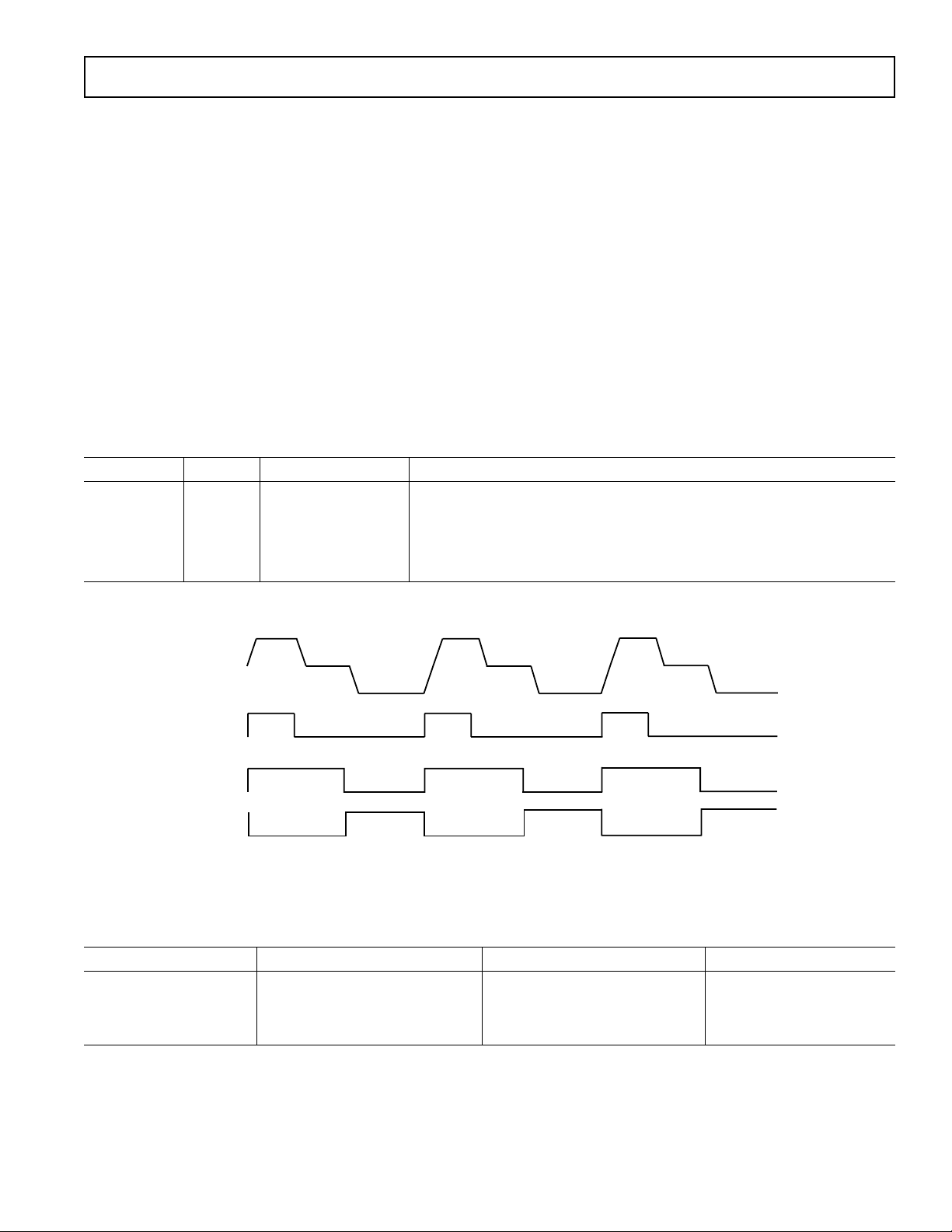
H-Driver and RG Outputs
In addition to the programmable timing positions, the AD9891/
AD9895 features on-chip output drivers for the RG and H1–H4
outputs. These drivers are powerful enough to directly drive the
CCD inputs. The H-driver current can be adjusted for optimum
rise/fall time into a particular load by using the DRV Registers
(Addr x0E1 to x0E4). The RG drive current is adjustable using
the RGDRV Register (Addr x0E8). Each 3-bit DRV Register is
adjustable in 3.5 mA increments, with the minimum setting of 0
equal to OFF or three-state, and the maximum setting of 7
equal to 24.5 mA.
As shown in Figure 11, the H2 and H4 outputs are inverses of
H1 and H3, respectively. The internal propagation delay resulting
from the signal inversion is less than 1 ns, which is significantly
less than the typical rise time driving the CCD load. This results
Table I. H1–H4, RG, SHP, and SHD Timing Parameters
in an H1/H2 crossover voltage at approximately 50% of the output swing. The crossover voltage is not programmable.
Digital Data Outputs
The AD9891/AD9895 data output and DCLK phase are programmable using the DOUTPHASE Register (Addr x01D). Any
edge from 0 to 47 may be programmed, as shown in Figure 12.
Normally, the DOUT and DCLK signals will track in phase,
based on the DOUTPHASE Register contents. The DCLK
output phase can also be held fixed with respect to the data
outputs, by changing the DCLKMODE Register (Addr x01E)
HIGH. In this mode, the DCLK output will remain at a fixed
phase equal to CLO (the inverse of CLI) while the data output
phase is still programmable.
There is a fixed output delay from the DCLK rising edge to the
DOUT transition, called t
. This delay can be programmed to
OD
four values between 0 ns and 12 ns, using the DOUT_DELAY
Register (Addr x032). The default value is 8 ns.
Register Length Range Description
POL 1b High/Low Polarity Control for H1, H3, and RG (0 = No Inversion, 1 = Inversion)
POSLOC 6b 0–47 Edge Location Positive Edge Location for H1, H3, and RG
Sample Location for SHP, SHD
NEGLOC 6b 0–47 Edge Location Negative Edge Location for H1, H3, and RG
DRV 3b 0–7 Current Steps Drive Current for H1–H4 and RG Outputs (3.5 mA per Step)
CCD
SIGNAL
RG
H1/H3
H2/H4
USING THE SAME TOGGLE POSITIONS FOR H1 AND H3 GENERATES STANDARD 2-PHASE H-CLOCKING.
Figure 9. 2-Phase H-Clock Operation
Table II. Precision Timing Edge Locations
Quadrant Edge Location (Dec) Register Value (Dec) Register Value (Bin)
I0 to 11 0 to 11 000000 to 001011
II 12 to 23 16 to 27 010000 to 011011
III 24 to 35 32 to 43 100000 to 101011
IV 36 to 47 48 to 59 110000 to 111011
REV. A
–13–
AD9891/AD9895
POSITION
PIXEL
PERIOD
RG
H1/H3
CCD
SIGNAL
NOTES
ALL SIGNAL EDGES ARE FULLY PROGRAMMABLE TO ANY OF THE 48 POSITIONS WITHIN ONE PIXEL PERIOD.
DEFAULT POSITIONS FOR EACH SIGNAL ARE SHOWN.
P[0]
RGr[0]
Hr[0]
RGf[12]
P[24]P[12] P[36]
Hf[24]
SHP[28]
t
S1
Figure 10. High Speed Clock Default and Programmable Locations
t
H1/H3
H2/H4
RISE
P[48] = P[0]
SHD[48]
t
<
t
PD
RISE
H1/H3
FIXED CROSSOVER VOLTAGE
t
PD
Figure 11. H-Clock Inverse Phase Relationship
P[0] P[48] = P[0]
PIXEL
PERIOD
DCLK
t
OD
DOUT
NOTES
DATA OUTPUT (DOUT) AND DCLK PHASE ARE ADJUSTABLE WITH RESPECT TO THE PIXEL PERIOD.
WITHIN 1 CLOCK PERIOD, THE DATA TRANSITION CAN BE PROGRAMMED TO 48 DIFFERENT LOCATIONS.
OUTPUT DELAY (
t
) FROM DCLK RISING EDGE TO DOUT RISING EDGE IS PROGRAMMABLE.
OD
P[12] P[24] P[36]
Figure 12. Digital Output Phase Adjustment
H2/H4
REV. A–14–
AD9891/AD9895
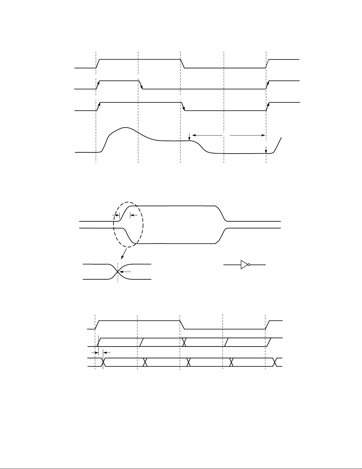
HORIZONTAL CLAMPING AND BLANKING
The AD9891/AD9895’s horizontal clamping and blanking pulses
are fully programmable to suit a variety of applications. As with
the vertical timing generation, individual sequences are defined
for each signal, which are then organized into multiple regions
during image readout. This allows the dark pixel clamping and
blanking patterns to be changed at each stage of the readout in
order to accommodate different image transfer timing and high
speed line shifts.
Individual CLPOB, CLPDM, and PBLK Sequences
The AFE horizontal timing consists of CLPOB, CLPDM, and
PBLK, as shown in Figure 13. These three signals are independently programmed using the registers in Table III. SPOL is
the start polarity for the signal, and TOG1 and TOG2 are the
first and second toggle positions of the pulse. All three signals
are active low and should be programmed accordingly. Up to
four individual sequences can be created for each signal.
HD
123
CLPOB
CLPDM
PBLK
PROGRAMMABLE SETTINGS:
1: START POLARITY (CLAMP AND BLANK REGION ARE ACTIVE LOW)
2: 1ST TOGGLE POSITION
3: 2ND TOGGLE POSITION
CLAMP CLAMP
Figure 13. Clamp and Preblank Pulse Placement
To simplify the programming requirements, the CLPDM signal
will track the CLPOB signal by default. If separate control of
the CLPDM signal is desired, the SINGLE_CLAMP Register
(Addr x031) should be set LOW.
Individual HBLK Sequences
The HBLK programmable timing shown in Figure 14 is similar
to CLPOB, CLPDM, and PBLK. However, there is no start
polarity control. Only the toggle positions are used to designate
the start and the stop positions of the blanking period. Additionally, there is a polarity control, HBLKMASK, that designates the
polarity of the horizontal clock signals H1–H4 during the blanking period. Setting HBLKMASK high will set H1 = H3 = Low
and H2 = H4 = High during the blanking, as shown in Figure 15.
Up to four individual sequences are available for HBLK.
Horizontal Sequence Control
The AD9891/AD9895 use sequence change positions (SCP)
and
sequence pointers (SPTR) to organize the individual hori-
HD
12
HBLK
PROGRAMMABLE SETTINGS:
1: 1ST TOGGLE POSITION = START OF BLANKING
2: 2ND TOGGLE POSITION = END OF BLANKING
BLANK BLANK
Figure 14. Horizontal Blanking (HBLK) Pulse Placement
HD
HBLK
H1/H3
H1/H3
H2/H4
THE POLARITY OF H1 DURING BLANKING IS PROGRAMMABLE (H2 IS OPPOSITE POLARITY OF H1)
REV. A
Figure 15. HBLK Masking Control
–15–
AD9891/AD9895
zontal
sequences. Up to four SCPs are available to divide the
readout into four separate regions, as shown in Figure 16. The
SCP0 is always hard-coded to line 0, and SCP1–SCP3 are
register programmable. During each region bound by the SCP,
the
SPTR Registers designate which sequence is used by each
signal.
CLPOB and CLPDM share the same SCP, PBLK has a
separate
set of SCP, and HBLK shares the vertical RCP (see
Vertical Timing Generation section). For example,
CLPSCP1 will define Region 0 for CLPOB and CLPDM,
and in that region
CLPDM sequences may be selected with the
The next SCP defines a new
any of the four individual
CLPOB and
region, and in that region each
SPTR Registers.
signal can be assigned to a different individual sequence. Because HBLK shares the vertical RCP, there are up to eight
regions where HBLK sequences may be changed using the eight
HBLKSPTR Registers.
Table III. CLPOB, CLPDM, and PBLK Individual Sequence Parameters
Register Length Range Description
SPOL 1b High/Low Starting Polarity of Vertical Transfer Pulse for Sequences 0–3
TOG1 12b 0–4095 Pixel Location First Toggle Position within Line for Sequences 0–3
TOG2 12b 0–4095 Pixel Location Second Toggle Position within Line for Sequences 0–3
Table IV. HBLK Individual Sequence Parameters
Register Length Range Description
HBLKMASK 1b High/Low Masking Polarity for H1 for Sequences 0–3 (0 = H1 Low, 1 = H1 High)
HBLKTOG1 12b 0–4095 Pixel Location First Toggle Position within Line for Sequences 0–3
HBLKTOG2 12b 0–4095 Pixel Location Second Toggle Position within Line for Sequences 0–3
Table V. Horizontal Sequence Control Parameters for CLPOB, CLPDM, and PBLK
Register Length Range Description
SCP1–SCP3 12b 0–4095 Line Number CLPOB/PBLK SCP to Define Horizontal Regions 0–3
SPTR0–SPTR3 2b 0–3 Sequence Number Sequence Pointer for Horizontal Regions 0–3
Table VI. Horizontal Sequence Control Parameters for HBLK
Register Length Range Description
VTPRCP1– 12b 0–4095 Line Number Vertical Region Change Positions (See Table IX.)
VTPRCP7
HBLKSPTR0– 2b 0–3 Sequence Number Sequence Pointer for HBLK Regions 0–7
HBLKSPTR7
SEQUENCE CHANGE POSITION #0
SEQUENCE CHANGE POSITION #1
SEQUENCE CHANGE POSITION #2
SEQUENCE CHANGE POSITION #3
UP TO FOUR INDIVIDUAL HORIZONTAL CLAMP AND BLANKING REGIONS MAY BE PROGRAMMED WITHIN A SINGLE FIELD, USING THE SEQUENCE CHANGE POSITIONS.
(V-COUNTER = 0)
SINGLE FIELD (1 VD INTERVAL)
CLAMP AND PBLK SEQUENCE REGION 1
CLAMP AND PBLK SEQUENCE REGION 2
CLAMP AND PBLK SEQUENCE REGION 3
CLAMP AND PBLK SEQUENCE REGION 4
Figure 16. Clamp and Blanking Sequence Flexibility
REV. A–16–
AD9891/AD9895
VERTICAL TIMING GENERATION
The AD9891/AD9895 provide a very flexible solution for generating vertical CCD timing and can support multiple CCDs and
different system architectures. The 4-phase vertical transfer
clocks V1–V4 are used to shift each line of pixels into the horizontal output register of the CCD. The AD9891/AD9895 allow
these outputs to be individually programmed into different pulse
patterns. Vertical sequence control registers then organize the
individual vertical pulses into the desired CCD vertical timing
arrangement.
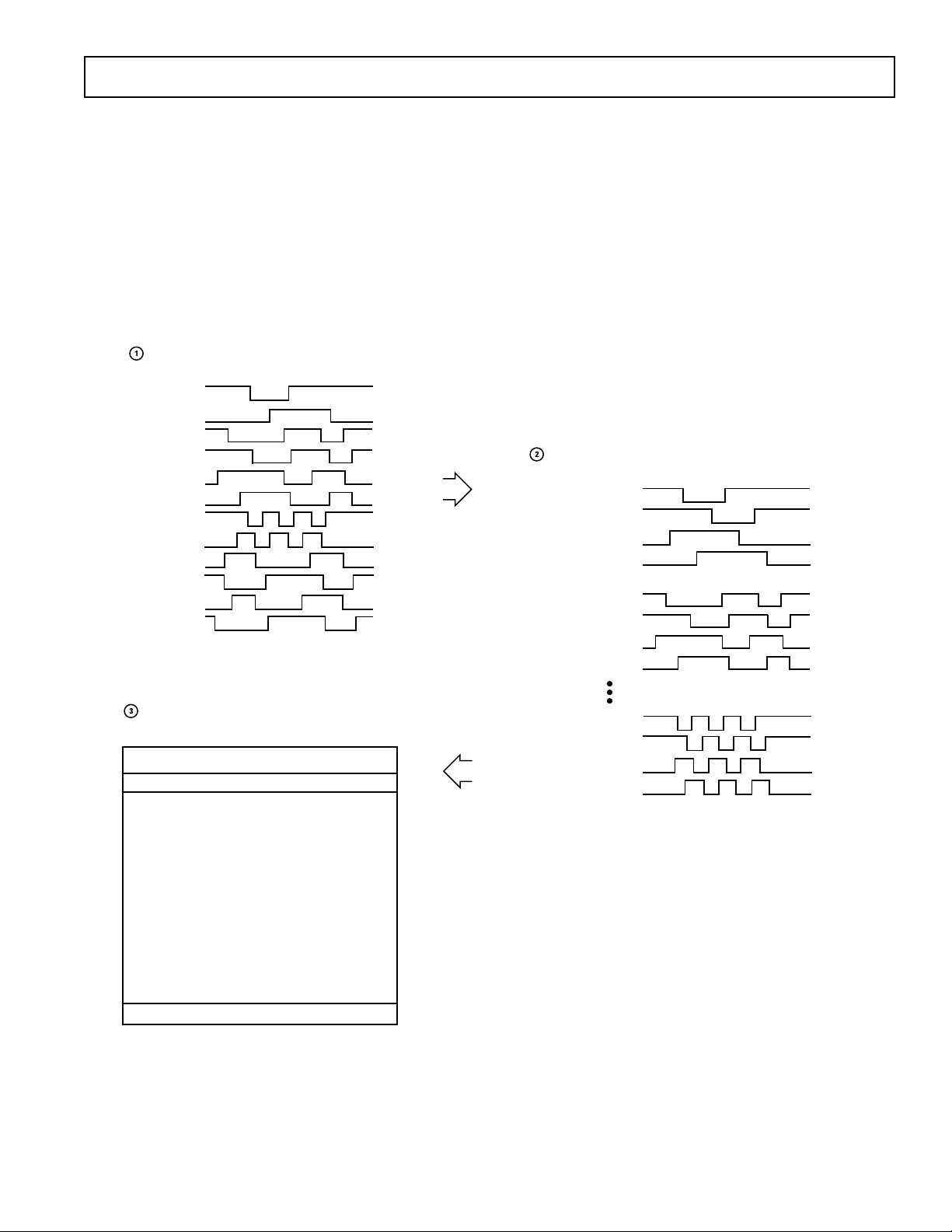
Figure 17 shows an overview of how the vertical timing is generated in three basic steps. First, the individual pulse patterns or
CREATE THE INDIVIDUAL VERTICAL
SEQUENCES (MAXIMUM OF 12 SEQUENCES).
SEQUENCE 0
SEQUENCE 1
SEQUENCE 2
SEQUENCE 3
SEQUENCE 4
SEQUENCE 5
SEQUENCE 6
SEQUENCE 7
SEQUENCE 8
SEQUENCE 9
SEQUENCE 10
SEQUENCE 11
sequences are created by using the Vertical Transfer Pulse (VTP)
Registers. These sequences are a essentially a “pool” of pulse
patterns that may be assigned to any of the V1-V4 outputs. Second, individual regions are built by assigning a sequence to each
of the V1–V4 outputs. Up to five unique regions may be specified. Finally, the readout of the entire field is constructed by
combining one or more of the individual regions sequentially.
With up to eight region areas available, different steps of the
readout such as high speed line shifts and vertical image transfer
can be supported.
BUILD THE INDIVIDUAL VERTICAL REGIONS BY ASSIGNING
EACH SEQUENCE TO V1–V4 OUTPUTS (MAXIMUM OF 5 REGIONS).
REGION 0 V1 (SEQ 0)
V2 (SEQ 0*)
V3 (SEQ 1)
V4 (SEQ 1*)
REGION 1 V1 (SEQ 2)
V2 (SEQ 3)
V3 (SEQ 4)
V4 (SEQ 5)
BUILD THE ENTIRE FIELD READOUT BY COMBINING
MULTIPLE REGIONS (MAXIMUM OF 8 COMBINATIONS).
USE REGION 2 FOR LINES 1 TO 20
USE REGION 1 FOR LINE 21
USE REGION 0 FOR LINES 22 TO 2000
USE REGION 2 FOR LINES 2001 TO 2020
Figure 17. Summary of Vertical Timing Generation
REGION 4 V1 (SEQ 6)
V2 (SEQ 6*)
V3 (SEQ 7)
V4 (SEQ 7*)
*SEQUENCES MAY BE SHIFTED AND/OR INVERTED
REV. A
–17–
AD9891/AD9895
Individual Vertical Sequences
To generate the individual vertical sequences or patterns shown
in Figure 18, five registers are required for each sequence.
Table VII summarizes these registers and their respective bit
lengths.
polarity of
The start polarity (VTPPOL) determines the starting
the vertical sequence and can be programmed high
or low. The first toggle position (VTPTOG1) and second
toggle position (VTPTOG2) are the pixel locations within the
line
where the pulse transitions. A third toggle position
(VTPTOG3) is also available for sequences 0 through 7. All
toggle positions are 10-bit values, which limits the placement of
a pulse to within 1024 pixels of a line. A separate register,
VSTART, sets the start position of the sequence within the line
(see Individual Vertical Regions section). The Length
(VTPLEN) Register determines the number of pixels between
each of the pulse repetitions, if any repetitions have been
programmed. The number of repetitions (VTPREP) simply
determines the number of pulse repetitions desired within a
single line. Programming “1” for VTPREP gives a single
pulse, while setting to “0” will provide a fixed dc output based
on the start polarity value. There is a total of 12 individual
sequences that may be programmed.
When specifying the individual regions, each sequence may be
assigned to any of the V1–V4 outputs. For example, Figure 19
shows a typical 4-phase V-clock arrangement. Two different
sequences are needed to generate the different pulsewidths.
The use of individual start positions for V1–V4 allows the four
outputs to be generated from two sequences. Figure 20 shows a
slightly different V-clock arrangement in which V2, V3, and V4
are simply shifted and/or inverted versions of V1. Only one
individual sequence is needed because all signals have the same
pulsewidth. The invert sequence registers (VINV) are used for
V3 and V4 (see Table VII).
Note that for added flexibility, the VTPPOL Registers (Start
Polarity) may be used as an extra toggle position.
Table VII. Individual VTP Sequence Parameters
Register Length Range Description
VTPPOL 1b High/Low Starting Polarity of Vertical Transfer Pulse for Each Sequence 0–11
VTPTOG1 10b 0–1023 Pixel Location First Toggle Position within Line for Each Sequence 0–11
VTPTOG2 10b 0–1023 Pixel Location Second Toggle Position within Line for Each Sequence 0–11
VTPTOG3 10b 0–1023 Pixel Location Third Toggle Position within Line for Each Sequence 0–7
VTPLEN 10b 0–1023 Pixels Length between Pulse Repetitions for Each Sequence 0–11
VTPREP 12b 0–4095 Pulses Number of Pulse Repetitions for Each Sequence 0–11 (0 = DC Output)
START POSITION OF SEQUENCE IS INDIVIDUALLY PROGRAMMABLE FOR EACH V1–V4 OUTPUT
HD
5
4
V1–V4
PROGRAMMABLE SETTINGS FOR EACH SEQUENCE:
1: START POLARITY
2: 1ST TOGGLE POSITION
3: 2ND TOGGLE POSITION (THERE IS ALSO A 3RD TOGGLE POSITION AVAILABLE FOR SEQUENCES 0 TO 7)
4: LENGTH BETWEEN REPEATS
5: NUMBER OF REPEATS
1
3
2
Figure 18. Individual Vertical Sequence Programmability
HD
V1
V2
V3
V1 USES SEQUENCE 0
V2 USES SEQUENCE 0,
WITH DIFFERENT START POSITION
V3 USES SEQUENCE 1
V4
V4 USES SEQUENCE 1,
WITH DIFFERENT START POSITION
Figure 19. Example of Separate V1–V4 Signals Using Two Individual Sequences
REV. A–18–

AD9891/AD9895
Individual Vertical Regions
The AD9891/AD9895 arranges the individual sequences into regions through
region, different
the use of Sequence Pointers (SPTR). Within each
sequences may be assigned to each V-clock
output. Figure 21 shows the programmability of each region
and Table VIII summarizes the registers needed for generating
each region.
For each individual region, the line length (in pixels) is programmable
using the HDLEN Registers. Each region can have a different
line
length to accommodate various image readout techniques.
maximum number of pixels per line is 4096. Also unique to
The
each
region are the sequence start positions for each V-output,
which are programmed using the VSTART Registers. Each
VSTART is a 12-bit value, allowing the start position to be
placed anywhere in the line. There are five HDLEN Registers,
one for each region. There is a total of 20 VSTART Registers:
The Sequence Pointer registers VxSPTRFIRST and
VxSPTRSECOND assign the individual vertical sequences to
each of the V-clock outputs (V1–V4) within a given region.
Typically, only the SPTRFIRST Registers are used, with the
SPTRSECOND Registers reserved for generating line-by-line
alternation (see Vertical Sequence Alternation). Any of the 12
individual sequences may also be inverted using the
VxINVFIRST and VxINVSECOND Registers, effectively doubling the number of sequences available. There is one
SPTRFIRST Register for each V-output, for a total of four registers per region. If all five regions are used, there is a total of 20
SPTRFIRST Registers. There is also the same number of
SPTRSECOND Registers, if alternation is required.
SPTR Registers are four bits wide; if a value greater than 11 is
programmed, the Vx output will be dc at the level of the
VxINV Register.
one for each V1–V4 output, for five different regions.
Note that the last line of the field is separately programmable
using the HDLASTLEN Register.
HD
V1
Note that the
V1 USES SEQUENCE 2
V2
V3
V4
Figure 20. Example of Inverted V1–V4 Signals Using One Individual Sequence with Inversion
1
HD
2
3
V1–V4
PROGRAMMABLE SETTINGS FOR EACH REGION:
1: START POSITION OF SELECTED SEQUENCE IS SEPARATELY PROGRAMMABLE FOR EACH OUTPUT
2: HD LINE LENGTH
3: SEQUENCE POINTERS (SPTR) TO SELECT AN INDIVIDUAL SEQUENCE FOR EACH OUTPUT
4: ANY SEQUENCES MAY ALSO BE ALTERNATED FOR ADDITIONAL FLEXIBILITY
SEQUENCES A, B, C, D
Figure 21. Individual Vertical Region Programmability
V2 USES SEQUENCE 2,
WITH DIFFERENT START POSITION
V3 USES SEQUENCE 2, INVERTED
V4 USES SEQUENCE 2, INVERTED,
WITH DIFFERENT START POSITION
REV. A
–19–

AD9891/AD9895
SINGLE FIELD (1 VD INTERVAL)
Table VIII. Individual Vertical Region Parameters
Register Length Range Description
HDLEN 12b 0–4095 Pixels HD Line Length for Lines in Each Region 0–4
VxSTART 12b 0–4095 Pixel Location Sequence Start Position for Each Vx Output in Each Region 0–4
VxSPTRFIRST 4b Sequence 0–11 Sequence Pointer for Vx Output during Each Region 0–4
(Can Be Used with SPTRSECOND for Alternation, See Text)
VxINVFIRST 1b High/Low When High, the Polarity of Sequence VxSPTRFIRST Is Inverted
x is the V-output from 1–4.
Complete Field: Combining the Regions
The individual regions are combined into a complete field readout
by using region change positions (RCP) and region pointers
(REGPTR). Figure 22 shows how each field is divided into
multiple regions. This allows the user to change the vertical
timing during various stages of the image readout. The boundaries
of each region are defined by the sequence change positions
(RCP). Each RCP is a 12-bit value representing the line number
bounding the region. A total of seven RCPs allow up to eight
REGION CHANGE POSTION #0
REGION CHANGE POSTION #1
REGION CHANGE POSTION #2
REGION CHANGE POSTION #3
REGION CHANGE POSTION #4
REGION CHANGE POSTION #5
REGION CHANGE POSTION #6
REGION CHANGE POSTION #7
(V-COUNTER = 0)
USE THE REGION SPECIFIED BY REGION POINTER 0
USE THE REGION SPECIFIED BY REGION POINTER 1
USE THE REGION SPECIFIED BY REGION POINTER 2
USE THE REGION SPECIFIED BY REGION POINTER 3
USE THE REGION SPECIFIED BY REGION POINTER 4
USE THE REGION SPECIFIED BY REGION POINTER 5
USE THE REGION SPECIFIED BY REGION POINTER 6
USE THE REGION SPECIFIED BY REGION POINTER 7
different region areas in the field to be defined. The first RCP is
always hard-coded to zero, and the remaining seven are register
programmable. Note that there are only five possible individual
regions that can be defined, but the eight region areas allow the
same region to be used in more than one place during the field.
Within each region area, the region pointers specify which of the
five individual regions will be used. There are eight region
pointers, one for each region area. Table IX summarizes
the
registers for the region change positions and region pointers.
UP TO EIGHT V-CLOCK REGION AREAS MAY BE DEFINED WITHIN ONE FIELD BY
USING THE REGION CHANGE POSITION AND THE REGION POINTERS.
Figure 22. Complete Field Using Multiple Region Areas
Table IX. Complete Vertical Field Registers
Register Length Range Description
VTPRCP 12b 0–4095 Line Location Region Change Position for each Region Area in Field
VTPREGPTR 3b Region 0–4Region Pointer for each Region Area of Field
REV. A–20–

AD9891/AD9895
Vertical Sequence Alternation
The AD9891/AD9895 also supports line-by-line alternation of
vertical sequences within any region, as shown in Figure 23.
Table X summarizes the additional registers used to support different alternation patterns. To create an alternating vertical pattern,
REGION CHANGE POSTION #0
ONLY FIRST LINES ARE USED
REGION CHANGE POSITION #1
FIRST LINES
SECOND LINES
REGION CHANGE POSTION #2
ONLY FIRST LINES ARE USED
WHEN THE VTPALT REGISTER IS LOW (NO ALTERNATION), ONLY THE FIRST LINES ARE USED.
SINGLE FIELD (1 VD INTERVAL)
Figure 23. Use of Line Alteration in Vertical Sequencing
USE F IRST V SEQUENCES
HD
USE SECOND V SEQUENCES
the VxSPTRFIRST and VxSPTRSECOND Registers are programmed with the desired sequences to be alternated. The
VTPALT Register must be set HIGH for that region to use
alternation. If VTPALT is LOW, then the VxSPTRSECOND
Registers will be ignored. Figure 24 shows an example of lineby-line alternation.
NO ALTERNATION
LINE-BY-LINE ALTERNATION
NO ALTERNATION
USE F IRST V SEQUENCES
V1
V2
V3
V4
SEQUENCES MAY BE ALTERNATED WITHIN A REGION BY USING THE SPTRFIRST AND SPTRSECOND REGISTERS.
Figure 24. Example of Line Alteration within a Region
Table X. Vertical Sequence Alternation Parameters
Register Length Range Description
VTPALT 1b Enabled/Disabled Enables the Line-by-Line Alternation (1 = Enabled)
VxSPTRFIRST 4b Sequence 0–11 SPTR for Vx Output during Each Region 0–4 for FIRST Lines
VxINVFIRST 1b High/Low When High, the Polarity of VxSPTRFIRST Is Inverted
VxSPTRSECOND 4b Sequence 0–11 SPTR for Vx Output during Each Region 0–4 for SECOND Lines
VxINVSECOND 1b High/Low When High, the Polarity of VxSPTRSECOND Is Inverted
x is the V-output from 1–4.
REV. A
–21–

AD9891/AD9895
Second Vertical Sequence During VSG Lines
Most CCDs require additional vertical timing during the sensor
gate line. The AD9891/AD9895 supports the option to output a
second set of sequences for V1–V4 during the line when the sensor gates VSG1–VSG4 are active. Figure 25 shows a typical VSG
line, which includes two separate sets of vertical sequences on V1–
V4. The sequences at the start of the line are the same as those
generated in the previous line. But the second sequence only
occurs in the line where the VSG signals are active. To select the
sequences used for the second sequence, the registers in
Table XI are used. To enable the second set of sequences during
the VSG line, the VTP_SGLINEMODE is set HIGH. As with
the standard vertical regions, each V1–V4 output has an individual start position, programmed in the VxSTART_SGLINE
Registers. Each V1–V4 output can select from the pool of 12
unique sequences using individual sequence pointer registers,
VxSPTR_SGLINE. Also, any sequence may be inverted for a
particular V1–V4 output by using the VxINV_SGLINE Registers.
Vertical Sweep Mode Operation
The AD9891/AD9895 contains a special mode of vertical timing
operation called Sweep Mode. This mode is used to generate a
large number of repetitive pulses that span across multiple HD
lines. One example of where this mode may be needed is at the
start of the CCD readout operation. At the end of the image
exposure, but before the image is transferred by the sensor gate
pulses, the vertical interline CCD Registers should be “clean” of
all charge. This can be accomplished by quickly shifting out any
charge with a long series of pulses on the V1–V4 outputs. Depending on the vertical resolution of the CCD, up to two or
three thousand clock cycles will be needed to shift the charge out
of each vertical CCD line. This operation will span across multiple HD line lengths. Normally, the AD9891/AD9895 sequences
are contained within one HD
is enabled, the HD boundaries
finished. To enable Sweep Mode
the appropriate SWEEP (0–4) Registers to HIGH.
Figure 26 shows an example of the Sweep Mode operation. The
number of vertical pulses needed will depend on the vertical
resolution of the CCD. The V1–V4 output signals are generated
using the Individual Vertical Sequence Registers (shown in Table
VII). A single pulse is created using the first, second, and third
toggle positions, and then the number of repeats is set to the
number of vertical shifts required by the CCD. The maximum
number of repeats is 4096 in this mode, using the VTPREP
Register. This produces a pulse train of the appropriate length.
Normally, the pulse train would be truncated at the end of the
HD line length. But with Sweep Mode enabled for this region, the
HD boundaries will be ignored. In Figure 26, the sweep region
occupies 23 HD
normal sequence operation will resume
lines. After the Sweep Mode region is completed,
line length. But when Sweep Mode
will be ignored until the region is
within any region, program
in the next region
.
Table XI. Second Vertical Sequence Registers During SG Lines
Register Name Length Range Description
VTP_SGLINEMODE 1b HIGH/LOW To Turn on Second Sequences during SG Line, Set = HIGH
VxSTART_SGLINE 12b 0–4095 Pixel Location Sequence Start Position for Each Vx Output for SG Line Sequence
VxSPTR_SGLINE 4b 0–11 Sequence # Sequence Pointer for Vx Output during second SG Line Sequence
VxINV_SGLINE 1b HIGH/LOW When HIGH, the Polarity of Sequence VxSPTRFIRST Is Inverted
x is the V-output from 1–4.
REV. A–22–

AD9891/AD9895
HD
VSG1–
VSGX
V1
V2
V3
V4
V1–V4
VD
HD
SENS OR GATE LINE
2ND GROUP OF V-SEQUENCES ARE OUTPUT DURING VSG LINE
Figure 25. Example of Second Sequences During Sensor Gate Line
LINE 0 LINE 1
LINE 24 LINE 25LINE 2
REGION AREA 0 REGION AREA 2
REGION AREA 1: SWEEP REGION
Figure 26. Example of Sweep Region for High Speed Vertical Shift
REV. A
–23–

AD9891/AD9895
Vertical Multiplier Mode
To generate very wide vertical timing pulses, a vertical region may
be configured into Multiplier Mode. This mode uses the vertical
sequence registers in a slightly different manner. Multiplier Mode
can be used to support unusual CCD timing requirements, such as
vertical pulses that are wider than a single HD line length.
The start polarity and toggle positions are still used in the same
manner as the standard sequence generation, but the length is
used differently. Instead of using the pixel counter (HD counter)
to specify the toggle position locations (VTPTOG1, 2, 3) of the
sequence, VTP length (VTPLEN) is multiplied by the
VTPTOG position to allow very long sequences to be generated.
To calculate the exact toggle position, counted in pixels after the
start position:
Multiplier Toggle Position VTPTOG VTPLEN=×
Because the VTPTOG Register is multiplied by VTPLEN, the
resolution of the toggle position placement is reduced. If
VTPLEN = 4, the toggle position accuracy is now reduced to
4-pixel steps instead of single pixel steps. Table XII summarizes
how the Individual Vertical Sequence Registers are programmed for Multiplier Mode operation. Note that the bit
ranges for the VTPTOG and VTPREP Registers differ from the
normal operation shown in Table VII. In Multiplier Mode, the
VTPREP Register should always be programmed to the same
value as the highest toggle position register.
The example shown in Figure 27 illustrates this operation. The
first toggle position is 2 and the second toggle position is 9. In
Nonmultiplier Mode, this would cause the V-sequence to
toggle at pixel 2 and then pixel 9 within a single HD line. However, now toggle positions are multiplied by the VTPLEN = 4,
so the first toggle occurs at pixel count = 8, and the second toggle
occurs at pixel count = 36. Sweep Mode should be enabled to
allow the toggle positions to cross the HD line boundaries.
Frame Transfer CCD Mode
The AD9891/AD9895 may also be configured for use with frame
transfer CCDs. In Frame Transfer CCD (FTCCD)
an
additional four vertical outputs are available for a total of
Mode,
eight outputs (V1–V8). In this case, V1–V4 are used for clocking the active image area, and V5–V8 are used for clocking the
storage area. In FTCCD Mode, the sequences assigned to the
V1–V4
storage
masking
outputs are duplicated at the V5–V8 outputs to allow the
area to be clocked along with the image area. Individual
of the V1–V4 and V5–V8 outputs allows for vertical
decimation techniques during transfer from the image to the
storage area.
of the sensor
an example of
The additional outputs V5–V8 are available on four
gate output pins, VSG1–VSG4. Figure 28 shows
the eight V-clocks configured for use with a frame
transfer CCD.
START POSITION OF SEQUENCE IS INDIVIDUALLY PROGRAMMABLE FOR EACH V1–V4 OUTPUT
HD
3
VTPLEN
PIXELS
V1–V4
MULTIPLIER MODE VERTICAL SEQUENCE PROPERTIES:
1: START POLARITY (ABOVE: STARTPOL = 0)
2: 1ST, 2ND, AND 3RD TOGGLE POSITIONS (ABOVE: VTPTOG1 = 2, VTPTOG2 = 9)
3: LENGTH OF VTP COUNTER (ABOVE: VTPLEN = 4). THIS IS THE MINIMUM RESOLUTION FOR TOGGLE POSITION CHANGES.
4: TOGGLE POSITIONS OCCUR AT LOCATION EQUAL TO (VTPTOG VTPLEN)
5: ENABLE SWEEP REGION ALLOWS THE COUNTERS TO CROSS THE HD BOUNDARIES
1234123412341234123412341234123412341234
1 2345678910111213141516171819202122232425262728293031323334353637383940
4
1
2
55
4
2
Figure 27. Example of Multiplier Region for Wide Vertical Pulse Timing
Table XII. Multiplier Mode and Sequence Register Parameters
Register Length Range Description
MULTI 1b HIGH/LOW High Enables Multiplier Mode for Each Region 0–4
VTPPOL 1b HIGH/LOW Starting Polarity of Vertical Transfer Pulse for Each Sequence 0–11
VTPTOG1 12b 0–4095 Pixel Location First Toggle Position for Each Sequence 0–11
VTPTOG2 12b 0–4095 Pixel Location Second Toggle Position for Each Sequence 0–11
VTPTOG3 12b 0–4095 Pixel Location Third Toggle Position for Each Sequence 0–7
VTPLEN 10b 0–1023 Pixels “Multiplier” Factor for Repetition Counter
VTPREP 12b 0–4096
Should Be Programmed to the Same Value as the Highest Toggle Position
REV. A–24–

HD
AD9891/AD9895
V1
ACTIVE
IMAGE
AREA
STORAGE
AREA
V2
V3
V4
V5
V6
V7
V8
Figure 28. Example of Frame Transfer CCD Mode using V1–V8
The frame transfer CCD also requires additional timing con
trol
when decimating the image for Preview Mode. The
AD9891/AD9895 contain registers to independently stop the
operation of the V5–V8 outputs while the V1–V4 outputs continue to run or to stop the V1–V4 outputs, while the V5–V8
outputs remain operational. The FREEZE and RESUME Registers specify the pixel locations within each line of a region where
the V1–V4 or V5–V8 clock outputs will start to hold their state,
where they will resume normal operation. FREEZE and
and
RESUME can be used in any region during the frame readout.
V1 USES SEQUENCE 0
V2 USES SEQUENCE 0
V3 USES SEQUENCE 1
V4 USES SEQUENCE 1
V5 USES SEQUENCE 0
V6 USES SEQUENCE 0
V7 USES SEQUENCE 1
V8 USES SEQUENCE 1
Vertical Sensor Gate (Shift Gate) Timing
With an interline CCD, the vertical sensor gates (VSG) are used to
transfer the pixel charges from the light-sensitive image area into the
light-shielded vertical registers. When a mechanical shutter is not being
used, this transfer will effectively end the exposure period during the
image acquisition. From the light-shield vertical registers, the image
is then read out line-by-line by using the vertical transfer pulses
V1–V4 in conjunction with the high speed horizontal clocks.
VD
4
HD
VSG1–VSG8
12 3
PROGRAMMABLE SETTINGS FOR EACH SEQUENCE:
1: START POLARITY OF PULSE 3: 2ND TOGGLE POSITION
2: 1ST TOGGLE POSITION 4: ACTIVE LINE FOR VSG PULSE WITHIN THE FIELD
Figure 29. Vertical Sensor Gate Pulse Placement
Table XIII. Sensor Gate Register Parameters
Register Length Range Description
SGPOL 1b High/Low Sensor Gate Starting Polarity for Sequence 0–3
SGTOG1 12b 0–4095 Pixel Location First Toggle Position for Sequence 0–11
SGTOG2 12b 0–4095 Pixel Location Second Toggle Position for Sequence 0–11
SGACTLINE 12b 0–4095 Pixel Location Line in Field where VSG1–VSG8 Are Active
SGSEL 2b Sequence 0–3 Selects Sequence 0–3 for VSG1–VSG8
SGMASK 8b 8 Individual Bits Masking for any of VSG1–VSG8 Signals (0 = On, 1 = Mask)
REV. A
–25–

AD9891/AD9895
Table XIII contains the summary of the VSG Registers. The
AD9891/AD9895 has eight SG outputs, VSG1–VSG8. Each of
the outputs can be assigned to one of four programmed
sequences by using the SGSEL1–SGSEL8 Registers. Each
sequence is generated in the same manner as the individual vertical
sequences, with a programmable
start polarity (SGPOL), first toggle
position (SGTOG1), and second toggle position (SGTOG2).
The active line where the VSG1–VSG8 pulses occur is programmable using the two SGACTLIN Registers. Additionally, any
of the VSG1–VSG8 pulses may be individually disabled by
using the SGMASK Register. The masking
allows all of the different SG sequences to be preprogrammed and the appropriate
pulses for odd or even fields can be masked.
ters (see Table XIV). The number of SUBCK pulses per field is
programmed in the SUBCKNUM Register.
As shown in Figure 30, the SUBCK pulses will always begin
on the line after the sensor gates occur, specified by the
SGACTLINE Register (Addr x265 and Addr x266). The
SUBCKPOL, SUBCK1TOG, SUBCK2TOG, and
SUBCKNUM Registers are updated at the start of the line after
the sensor gate line. All other shutter mode registers are updated with the majority of the AD9891/AD9895’s registers at
the VD/HD falling edge.
High Precision Shutter Mode
High precision shuttering is controlled in the same way as normal shuttering but requires a second set of toggle registers. In
SHUTTER TIMING CONTROL
CCD image exposure time is controlled through use of the substrate
clock signal (SUBCK), which pulses the CCD substrate to clear
out accumulated charge. The AD9891/AD9895 supports three
types of
sion Shutter
SUBCK pulse
electronic shuttering: Normal Shutter Mode, High Preci-
Mode, and Low Speed Shutter Mode. Along with the
placement, the AD9891/AD9895 can accommodate different progressive and interlaced readout modes.
Additionally, the AD9891/AD9895 provides
output signals to
control an external mechanical shutter, strobe (flash), and the
CCD bias for still mode readout (VSUB).
Normal Shutter Mode
Figure 30 shows the VD and SUBCK output for Normal Shutter Mode. The SUBCK will pulse once per line, and the total
number of repetitions within the field is programmable. The
pulse polarity, width, and line location is programmable using
this mode, the SUBCK still pulses once per line, but the last
SUBCK in the field will have an additional SUBCK pulse
whose location is determined by the SUBCK2TOG1 and
SUBCK2TOG2 Registers (see Figure 31). Finer resolution of
the exposure time is possible using this mode. Leaving both
SUBCK2TOG Registers set to 4095 (x3F) will disable the High
Precision Mode (default setting).
Low Speed Shutter Mode
For normal exposure times less than one field interval, the
EXPOSURE Register will be set to 0. Exposure times greater
than one field interval can be achieved by writing a value
greater than zero to the EXPOSURE Register. As shown in
Figure 32, this shutter mode will suppress the SUBCK and
VSG outputs for up to 4095 fields (VD periods). The VD and
HD outputs may be suppressed during the exposure period by
programming the VDHDOFF Register to 1.
the SUBCKPOL, SUBCK1TOG1, and SUBCK1TOG2 Regis-
VD
HD
VSG1–
VSG8
SUBCK
SUBCK PROGRAMMABLE SETTINGS:
1: PULSE POLARITY USING THE SUBCKPOL REGISTER
2: NUMBER OF PULSES WITHIN THE FIELD USING THE SUBCKNUM REGISTER
3: PIXEL LOCATION OF PULSE WITHIN THE LINE AND PULSE WIDTH PROGRAMMED USING SUBCK1 TOGGLE POSITION REGISTERS
t
EXP
t
EXP
Figure 30. Normal Shutter Mode
VD
HD
VSG1–
VSG8
SUBCK
NOTES
1. 2ND SUBCK PULSE IS ADDED IN THE LAST SUBCK LINE.
2. LOCATION OF 2ND PULSE IS FULLY PROGRAMMABLE USING THE SUBCK2 TOGGLE POSITION REGISTERS.
t
EXP
Figure 31. High Precision Shutter Mode
t
EXP
REV. A–26–

AD9891/AD9895
SUBCK Suppression
Normally, the SUBCKs will begin to pulse on the line following
the sensor gate line (VSG). With some CCDs, the SUBCKs
need to be suppressed for one or more lines following the VSG
line. The SUBCKSUPPRESS Register allows for the suppression
the SUBCK pulses for up to 63 lines following the VSG line.
Readout After Exposure
A write to the EXPOSURE Register will designate the number
fields in the exposure time (t
) from 0 to 4095. After the exposure,
EXP
the readout of the CCD data occurs. During readout, the
SUBCK
output may need to be further suppressed until the
readout is completed. The READOUT Register specifies the
number of additional fields after the exposure to continue the
suppression of SUBCK. READOUT can be programmed for
zero to seven additional fields and should be preprogrammed at
start-up, not
interlaced CCD
at the same time as the exposure write. A typical
frame readout mode will generally require two
additional fields of SUBCK suppression (READOUT = 2).
Note that a write to the EXPOSURE Register acts as a trigger
for
readout after the exposure is completed. If no write to the
EXPOSURE Register occurs, than the READOUT Register will
have no effect. See Figure 35 for an example of triggering the
exposure and subsequent readout.
VSUB Control
The CCD readout bias (VSUB) can be programmed to accommodate different CCDs. Figure 35 shows two different modes
that are available. In Mode 0, VSUB goes active during the
field of the last SUBCK when the exposure begins. The
on-position
line within the
(rising edge in Figure 35) is programmable to any
field. VSUB will remain active until the end of
the image readout. In Mode 1, the VSUB is not activated
until the start of the readout.
MSHUT and STROBE Control
MSHUT and STROBE operation is shown in Figures 33, 34,
and 35. Table XV shows the registers parameters for controlling the MSHUT and STROBE outputs. The MSHUT output
is switched on with the MSHUTON Registers, and it will
remain on until the location specified in the MSHUTOFF
Registers.
anywhere
The location of MSHUTOFF is fully programmable to
within the exposure period, using the FD (field), LN
(line), and PX (pixel) Registers. The STROBE pulse is defined
by the ON and OFF positions. STROBON_FD is the field in
which the STROBE is turned on, measured from the field containing the last SUBCK before exposure begins. The
STROBON_ LN and STROBON_PX Registers give the line
and pixel positions with respect to STROBON_FD. The
STROBE off position is programmable to any field, line, and
pixel location with respect to the field of the last SUBCK.
VD
VSG1–
VSG8
SUBCK
NOTES
1. SUBCK MAY BE SUPPRESSED FOR MULTIPLE FIELDS BY PROGRAMMING THE EXPOSURE REGISTER GREATER THAN ZERO.
2. ABOVE EXAMPLE USES EXPOSURE = 1.
3. VD/HD OUTPUTS MAY ALSO BE SUPPRESSED USING THE VDHDOFF REGISTER = 1.
t
EXP
Figure 32. Low Speed Shutter Mode Using EXPOSURE Register
Table XIV. Electronic Shutter Mode Register Parameters
Register Length Range Description
SUBCKPOL* 1b HIGH/LOW SUBCK Start Polarity for SUBCK1 and SUBCK2
SUBCK1TOG1* 12b 0–4095 Pixel Location SUBCK First Toggle Position
SUBCK1TOG2* 12b 0–4095 Pixel Location SUBCK Second Toggle Position
SUBCK2TOG1* 12b 0–4095 Pixel Location Second SUBCK First Toggle Position (for High Precision Mode)
SUBCK2TOG2* 12b 0–4095 Pixel Location Second SUBCK Second Toggle Position (for High Precision Mode)
SUBCKNUM* 12b 0–4095 # of Pulses Total Number of SUBCKs per Field (at 1 Pulse per Line)
SUBCKSUPPRESS* 6b 0–63 # of Pulses Number of SUBCK’s to Suppress after VSG Line
EXPOSURE 12b 0–4095 # of Fields Number of Fields to Suppress to SUBCK and VSG;
Triggers Readout to Occur after t
EXP
VDHDOFF 1b ON/OFF Disable VD/HD Output during Exposure (1 = On, 0 = Off)
READOUT 3b 0–7 # of Fields
*Register is not VD/HD updated but is updated at the start of line after sensor gate line.
Number of Fields to Suppress SUBCK after Exposure (for Readout)
REV. A
–27–

AD9891/AD9895
3: OFF-POSITION CAN BE PROGRAMMED ANYWHERE FROM THE FIELD OF LAST SUBCK UNTIL THE FIELD BEFORE READOUT
VD
VSG1–
VSG8
SUBCK
MSHUT
1
2
MSHUT PROGRAMMABLE SETTINGS:
1: ACTIVE POLARITY
2: ON-POSITION IS VD UPDATED AND MAY BE SWITCHED ON AT ANY TIME
VD
VSG1–
VSG8
SUBCK
t
EXP
3
Figure 33. MSHUT Output Programmability
t
EXP
STROBE
STROBE PROGRAMMABLE SETTINGS:
1: ACTIVE POLARITY
2: ON-POSITION WITH RESPECT TO TO FIELD OF LAST SUBCK
3: OFF-POSITION CAN BE PROGRAMMED ANYWHERE DURING THE EXPOSURE TIME
1
2
3
Figure 34. STROBE Output Programmability
Table XV. VSUB, MSHUT, and STROBE Register Parameters
Register Length Range Description
TRIGGER 3b On/Off for Three Signals 1-Bit Triggers for VSUB[0], MSHUT[1], and STROBE[2]
VSUBMODE 1b HIGH/LOW VSUB Mode (0 = Mode 0, 1 = Mode 1) (See Figure 27)
VSUBKEEPON 1b HIGH/LOW Sets VSUB to Stay Active after Readout When High
VSUBPOL 1b HIGH/LOW VSUB Active Polarity
VSUBON 12b 0–4095 Line Location VSUB On Position. Active starting in any line of field.
MSHUTON 1b ON/OFF MSHUT Signal Enable (1 = Active or “Open”)
MSHUTONPOS_LN 12b 0–4095 Line Location MSHUT Line Location
MSHUTONPOS_LN 12b 0–4095 Pixel Location MSHUTON Pixel Location
MSHUTPOL 1b HIGH/LOW MSHUT Active Polarity
MSHUTOFF_FD 12b 0–4095 Field Location Field Location to Switch OFF MSHUT. (Inactive or “Closed”)
MSHUTOFF_LN 12b 0–4095 Line Location Line Location to Switch OFF MSHUT. (Inactive or “Closed”)
MSHUTOFF_PX 12b 0–4095 Pixel Location Pixel Location to Switch OFF MSHUT. (Inactive or “Closed”)
STROBPOL 1b HIGH/LOW STROBE Active Polarity
STROBON_FD 12b 0–4095 Field Location STROBE ON Field Location, with Respect to Last SUBCK Field
STROBON_LN 12b 0–4095 Line Location STROBE ON Line Location
STROBON_PX 12b 0–4095 Pixel Location STROBE ON Pixel Location
STROBOFF_FD 12b 0–4095 Field Location STROBE OFF Field Location, with Respect to Last SUBCK Field
STROBOFF_LN 12b 0–4095 Line Location STROBE OFF Location
STROBOFF_PX 12b 0–4095 Pixel Location STROBE OFF Location
REV. A–28–

SERIAL
WRITES
AD9891/AD9895
VD
VSG
t
SUBCK
STROBE
MSHUT
MECHANICAL
SHUTTER
VSUB
MODE 0
EXP
Figure 35. Exposure and Readout of Interlaced Frame
Example of Exposure and Readout of Interlaced Frame
Figure 35 shows the sequence of events for a typical exposure and
readout operation using a mechanical shutter and strobe. The
register values for the VSUB, MSHUT, and STROBE toggle
positions may be previously loaded at any time, prior to triggering
these functions. Additional register writes are required to configure
the vertical clock outputs, V1–V4, which are not described here.
0: Write to the READOUT Register (Addr x281) to specify
the number of fields to further suppress SUBCK while the
CCD data is readout. In this example, READOUT = 2.
1: Write to the EXPOSURE Register (Addr x27D) to start the
exposure and specify the number of fields to suppress
SUBCK and VSG outputs during exposure. In this example,
EXPOSURE = 2.
Write to the TRIGGER Register (Addr x280) to enable the
STROBE, MSHUT, and VSUB signals. To trigger all three
signals (as in Figure 36) the register TRIGGER = 7.
Write to the SGACTLINE Register (Addr x265 and
Addr x266) and SGMASK Register (Addr x26F and
Addr x270) to configure the sensor gates for ODD field
readout (interlaced CCD).
2: VD/HD falling edge will update the serial writes from 1.
3: If VSUB Mode = 0, VSUB output turns ON at the line
specified in the VSUBON Register (Addr x272 and
Addr x273).
ODD EVEN
IMAGE READOUT
OPEN
CLOSED
MODE 1
OPEN
STROBE output turns ON at the location specified in the
STROBON Registers (Addr x294 to Addr x299).
4: STROBE output turns OFF at the location specified in the
STROBEOFF Registers (Addr x29A to Addr x29F).
5: MSHUT Output turns OFF at the location specified in the
MSHUTOFF Registers (Addr x28D to Addr x292).
6: Write to the SGACTLINE Register (Addr x253 and
Addr x254) and SGMASK Register to configure the sensor
gates for EVEN field readout.
7: VD/HD falling edge will update the serial writes from 6.
8: Write to the SGACTLINE Register and SGMASK Register
to reconfigure the sensor gates for Draft/Preview Mode output.
Write to the MSHUTON Register (Addr x287) to reopen
the mechanical shutter for Draft/Preview Mode.
9: VD/HD falling edge will update the serial writes from 8.
10: VSG outputs returns to Draft/Preview Mode timing.
SUBCK output resumes operation.
MSHUT output returns to the ON position (Active or
“Open”).
VSUB output returns to the OFF position (Inactive).
REV. A
–29–

AD9891/AD9895
ANALOG FRONT END DESCRIPTION AND OPERATION
The AD9891/AD9895 AFE signal processing chain is shown in
Figure 36. Each processing step is essential in achieving a high
quality image from the raw CCD pixel data. AFE Register details are shown in Table XXXI.
DC Restore
To reduce the large dc offset of the CCD output signal, a dcrestore circuit is used with an external 0.1 µF series coupling
capacitor. This restores the dc level of the CCD signal to
approximately 1.5 V, to be compatible with the 3 V analog
supply of the AD9891/AD9895.
Correlated Double Sampler
The CDS circuit samples each CCD pixel twice to extract the
video
information and reject low frequency noise. The tim
ing
shown in Figure 10 illustrates how the two internally
generated CDS clocks, SHP and SHD, are used to sample
the reference level and the data level, respectively, of the
CCD signal. The placement of the SHP and SHD sampling
edges is determined by the setting of the SHPPOSLOC and
SHDPOSLOC Registers located at Addr 0xE9 and
Addr 0xEA,
respectively. Placement of these two clock signals
is critical in achieving the best performance from the CCD.
Input Clamp
A line-rate input clamping circuit is used to remove the CCD’s
optical black offset. This offset exists in the CCD’s shielded
black reference pixels. The AD9891/AD9895 remove this offset
input stage to minimize the effect of a gain change on the
in the
black level. Another advantage
system
the input stage is to maximize system
CCDs have large black level offset voltages,
rected at the input stage, can significantly reduce
headroom in the internal circuitry when higher VGA
of removing this offset at
headroom. Some area
which, if not cor-
the available
gain set-
tings are used.
The input clamp is controlled by the CLPDM signal, which is
fully programmable (see Horizontal Clamping and Blanking
section).
Timing Sequence Example
CLPDM pulse be used during
System timing examples are shown in the Horizontal
section. It is recommended that the
valid CCD dark pixels. CLPDM
may be used during the optical black pixels, either together
with CLPOB or separately. The CLPDM pulse should be a
minimum of 4 pixels wide.
PxGA
The PxGA provides separate gain adjustment for the individual color
pixels. A programmable gain amplifier with four separate values,
the PxGA has the capability to “multiplex” its gain value on a
pixel-to-pixel basis (see Figure 37). This allows lower output
color
pixels to be gained up to match higher output color pixels.
Also, the
reducing
different
PxGA may be used to adjust the colors for white balance,
the amount of digital processing that is needed. The four
gain values are switched according to the “color
steering” circuitry. Seven different color steering modes for different types of CCD color filter arrays are programmed in the
AD9891/AD9895 AFE CTLMODE Register, at Addr 0x06
(see Figures 39a–39g for internal color steering timing). For
0.1F
0.1F
0.1F
0.1F
CCDIN
BYP1
BYP2
BYP3
DC RESTORE
1.5V
SHP
CDS
SHD
–2dB TO +10dB
PxGA
CLPDM
INPUT OFFSET
CLAMP
Figure 36. AFE Block Diagram
0dB TO 36dB
SHP
SHD
PRECISION
TIMING
GENERATION
VGA
10
VGA GAIN
REGISTER
DOUT
PHASE
8-BIT
DAC
CLPDM
GENERATION
REFB
1.0V
OPTICAL BLACK
DIGITAL
FILTER
CLPOB PBLK
V-H
TIMING
1.0F
INTERNAL
V
REF
2V FULL
SCALE
ADC
CLAMP
1.0F
REFT
2.0V
CLPOB
8
CLAMP LEVEL
REGISTER
OUTPUT
DATA
LATCH
PBLK
DOUT
PHASE
10
or
12
DOUT
REV. A–30–

RR
Gb Gb
Gr
Gr
BB
CCD: PROGRESSIVE BAYER
LINE0 GAIN0, GAIN1, GAIN0, GAIN1, ...
RR
Gr
Gr
Gb GbBB
LINE1
LINE2
GAIN2, GAIN3, GAIN2, GAIN3, ...
GAIN0, GAIN1, GAIN0, GAIN1, ...
MOSAIC SEPARATE COLOR
STEERING MODE
VD
NOTES
1. FLD FALLING EDGE (START OF ODD FIELD) WILL RESET THE PxGA GAIN REGISTER STEERING TO “0101” LINE.
2. FLD RISING EDGE (START OF EVEN FIELD) WILL RESET THE PxGA GAIN REGISTER STEERING TO “2323” LINE.
3. HD FALLING EDGES WILL RESET THE PxGA GAIN REGISTER STEERING TO EITHER “0” (FLD = ODD) OR “2” (FLD = EVEN).
HD
00 00 22 2 0211 11 33 330011 2233XX
PxGA GAIN
REGISTER
FLD
ODD FIELD EVEN FIELD
example, the Mosaic Separate Steering Mode accommodates the
popular “Bayer” arrangement of Red, Green, and Blue filters
(see Figure 38a).
The same Bayer pattern can also be interlaced, and the Mosaic
Interlaced Mode should be used with this type of CCD (see
Figure 38b). The color steering performs the proper multiplexing of the R, G, and B gain values (loaded into the PxGA gain
registers) and is synchronized by the vertical (VD) and horizontal (HD) sync pulses. The PxGA gain for each of the four
channels is variable from –2dBto +10 dB, controlled in 64
steps through the serial interface. The PxGA gain curve is
shown in Figure 40.
VD
HD
SHP/SHD
6
PxGA
COLOR
STEERING
CONTROL
2
4:1
MUX
3
PxGA
STEERING
MODE
SELECTION
GAIN0
GAIN1
PxGA GAIN
REGISTERS
GAIN2
GAIN3
VGACDS
CONTROL
REGISTER
BITS D0:D2
Figure 37. PxGA Block Diagram
AD9891/AD9895
Figure 38a. CCD Color Filter Example: Progressive Scan
CCD: INTERLACED BAYER
EVEN FIELD
LINE0 GAIN0, GAIN1, GAIN0, GAIN1, ...
RR
Gr
RR
Gr
RR
Gr
RR
Gr
ODD FIELD
Gb GbBB
Gb GbBB
Gb GbBB
Gb GbBB
Gr
LINE1
Gr
Gr
LINE2
Gr
LINE0 GAIN2, GAIN3, GAIN2, GAIN3, ...
LINE1
LINE2
Figure 38b. CCD Color Filter Example: Interlaced
MOSAIC INTERLACED
COLOR STEERING MODE
GAIN0, GAIN1, GAIN0, GAIN1, ...
GAIN0, GAIN1, GAIN0, GAIN1, ...
GAIN2, GAIN3, GAIN2, GAIN3, ...
GAIN2, GAIN3, GAIN2, GAIN3, ...
FLD
VD
HD
PxGA GAIN
REGISTER
NOTES
1. VD FALLING EDGE WILL RESET THE PxGA GAIN REGISTER STEERING TO “0101” LINE.
2. HD FALLING EDGES WILL ALTERNATE THE PxGA GAIN REGISTER STEERING BETWEEN “0101” AND “2323” LINES.
3. FLD STATUS IS IGNORED.
00 00 00 0 0011 11 11 112233 2233XX
ODD FIELD EVEN FIELD
Figure 39a. Mosaic Separate Color Steering Mode
REV. A
Figure 39b. Mosaic Interlaced Color Steering Mode
–31–

AD9891/AD9895
FLD
VD
HD
GAIN
PxGA
REGISTER
NOTES
1. VD FALLING EDGE WILL RESET THE
2. HD FALLING EDGES WILL ALTERNATE THE
3. ALL FIELDS WILL HAVE THE SAME
00 00 00 0 0011 11 11 111122 1122XX
PxGA
PxGA
ODD FIELD EVEN FIELD
GAIN STEERING TO “0101” LINE.
GAIN STEERING BETWEEN “0101” AND “1212” LINES.
PxGA
GAIN STEERING PATTERN (FLD STATUS IS IGNORED).
Figure 39c. Mosaic Repeat Color Steering Mode
FLD
VD
HD
PxGA GAIN
REGISTER
NOTES
1. EACH LINE FOLLOWS “012012” STEERING PATTERN.
2. VD AND HD FALLING EDGES WILL RESET THE PxGA GAIN REGISTER STEERING TO GAIN REGISTER “0.”
3. FLD STATUS IS IGNORED.
02 02 02 0 0210 10 10 100210 0210XX
ODD FIELD EVEN FIELD
Figure 39d. 3-Color 1-Color Steering Mode
FLD
VD
HD
PxGA GAIN
REGISTER
NOTES
1. VD FALLING EDGE WILL RESET THE PxGA GAIN REGISTER STEERING TO “012012” LINE.
2. HD FALLING EDGES WILL ALTERNATE THE PxGA GAIN REGISTER STEERING BETWEEN “012012” AND “210210” LINES.
3. FLD STATUS IS IGNORED.
02 02 02 0 0210 10 10 102012 2012XX
ODD FIELD EVEN FIELD
Figure 39e. 3-Color 2-Color Steering Mode
FLD
VD
HD
PxGA GAIN
REGISTER
NOTES
1. EACH LINE FOLLOWS “01230123” STEERING PATTERN.
2. VD AND HD FALLING EDGES WILL RESET THE PxGA GAIN REGISTER STEERING TO GAIN REGISTER “0.”
3. FLD STATUS IS IGNORED.
02 02 02 0 0213 13 13 130213 0213XX
ODD FIELD EVEN FIELD
Figure 39f. 4-Color 1-Color Steering Mode
REV. A–32–

AD9891/AD9895
FLD
VD
HD
PxGA GAIN
REGISTER
NOTES
1. VD FALLING EDGE WILL RESET THE PxGA GAIN REGISTER STEERING TO “01230123” LINE.
2. HD FALLING EDGES WILL ALTERNATE THE PxGA GAIN REGISTER STEERING BETWEEN “01230123” AND “23012301” LINES.
3. FLD STATUS IS IGNORED.
02 02 02 0 0213 13 13 132031 2031XX
ODD FIELD EVEN FIELD
Figure 39g. 4-Color 2-Color Steering Mode
10
8
6
4
The VGA gain curve follows a “linear-in-dB” characteristic.
The exact VGA gain can be calculated for any gain register
value by using the equation:
where the code range is 0 to 1023. PxGA default gain is included.
The gain accuracy specifications include the PxGA gain of
2
PxGA GAIN – dB
0
–2
–4
40 48 58 0 8 16 24 31
32
(100000) (011111)
PxGA GAIN REGISTER CODE
Figure 40. PxGA Gain Curve
36
approximately
Optical Black Clamp
The optical black clamp loop is used to remove residual offsets
in the signal chain and to track low frequency variations in the
CCD’s black level. During the optical black (shielded) pixel
interval on each line, the ADC output is compared with a fixed
black level reference selected by the user in the Clamp Level
Register. The clamp level is programmable in 256 steps, with a
range between 0 LSB and 63.75 LSB in the AD9891 and between 0 LSB and 255 LSB in the AD9895. The resulting error
signal is filtered to reduce noise, and the correction value is
4 dB,
applied to the ADC input through a D/A converter. Normally,
30
24
18
VGA GAIN – dB
12
the optical black clamp loop is turned on once per horizontal
line, but this loop can be updated more slowly to suit a particular applica
the post-
tion. If external digital clamping is used during
processing, the AD9891/AD9895 optical black
clamping may be disabled using Bit D5 in the Operation Register (see Serial Interface Timing and Register Listing sections).
When the loop is disabled, the Clamp Level Register may still
be used to provide programmable offset adjustment.
The optical black clamp is controlled by the CLPOB signal,
6
which is fully programmable (see Horizontal Clamping and
Blanking section). System timing examples are shown in the
0
0
127
255 383 511 639 767 895
VGA GAIN REGISTER CODE
1023
Figure 41. VGA Gain Curve (PxGA not included)
Variable Gain Amplifier
The VGA stage provides a gain range of 2 dB to 36 dB, programmable with 10-bit resolution through the serial digital
interface. Combined with approximately 4 dB from the PxGA
stage, the total gain range for the AD9891/AD9895 is 6 dB to
40 dB. The minimum gain of 6 dB is needed to match a 1 V
input signal with the ADC full-scale range of 2 V. When compared to 1 V full-scale systems (such as ADI’s AD9803), the
equivalent gain range is 0 dB to 34 dB.
Horizontal Timing Sequence Example section. The CLPOB
pulse should be placed during the CCD’s optical black pixels. It
is recommended that the CLPOB pulse duration be at least
20 pixels wide. Shorter pulsewidths may be used, but the ability
to track low frequency variations in the black level will be
reduced.
A/D Converter
The AD9891 uses a high a performance 10-bit ADC architecture, optimized for high speed and low power, while the
AD9895 uses a 12-bit ADC architecture. Differential
nonlinearity (DNL) performance is typically better than
0.5 LSB for both products. The ADC uses a 2 V input range.
Better noise performance results from using a larger ADC fullscale range.
Gain Code=×+(. ) .0 035 3 55
for a total gain range of 6 dB to 40 dB.
REV. A
–33–

AD9891/AD9895
VDD
(INPUT)
CLI
(INPUT)
SERIAL
WRITES
SYNC
(INPUT)
VD
(OUTPUT)
HD
(OUTPUT)
DIGITAL
OUTPUTS
t
PWR
H2/H4
H1/H3, RG, DCLK
1 V
ODD FIELD EVEN FIELD
1 H
CLOCKS ACTIVE WHEN OUT_CONT REGISTER IS
UPDATED AT VD/HD EDGE
Figure 42. Recommended Power-Up Sequence and Synchronization, Master Mode
POWER-UP AND SYNCHRONIZATION
Recommended Power-Up Sequence for Master Mode
When the AD9891/AD9895 are powered up, the following
sequence is recommended (refer to Figure 42 for each step).
1. Turn on power supplies for the AD9891/AD9895.
2. Apply the master clock input CLI.
3. Reset and initialize the internal AD9891/AD9895 Registers.
First, write a “1” to the SW_RESET Register (Addr x017)
followed by a “0” to the same register. Next, write
“110101” (53 decimal) to the INITIAL1 Register
(Addr x02B) followed by “000100” (4 decimal) to the
INTIAL2 Register (Addr x010). This sequence of writes
must always be done in the proper order:
Addr x017 Data 000001
Addr x017 Data 000000
Addr x02B Data 110101
Addr x010 Data 000100
4. Configure the AD9891/AD9895 for Master Mode timing by
writing a “1” to the MASTER Register (Addr x0EB).
5. By default, the internal timing core is held in a reset state
with TGCORE_RSTB Register = “0.” Write a “1” to the
TGCORE_RSTB Register (Addr x029) to start the internal
timing core operation.
6. Write a “1” to the PREVENTUPDATE Register
(Addr x01B). This will prevent any updating of the serial
register data.
7. Write a “1” to the SYNCENABLE Register (Addr x024).
This will allow the external SYNC to be used.
8. Write a “1” to the SYNCSUSPEND Register (Addr x026).
This will cause the outputs to be suspended during the
SYNC operation (see Figure 43).
9. Write to desired registers to configure high speed timing,
horizontal timing, vertical timing, and shutter timing.
10. If SYNC is HIGH at power-up, then bring SYNC input
LOW. Also, SYNC may be held low from power-up.
11. Write a “1” to the OUT_CONT Register (Addr x018). This
will allow the outputs to become active after SYNC rising edge.
12. Write a “0” to the PREVENTUPDATE Register
(Addr x01B). This will allow the serial information to be updated at the next VD/HD falling edge.
13. Bring SYNC back HIGH. This will cause the internal
counters to reset to “0” and start VD/HD operation.
VD/HD edge allows register updates to occur, including
OUT_CONT, which enables all clock outputs.
SYNC During Master Mode Operation
The SYNC input may be used any time during operation to
resync the AD9891/AD9895 counters with external timing, as
shown in Figure 43. The operation of the digital outputs may
be suspended during the SYNC operation by setting the
SYNCSUSPEND Register (Addr x026) to a “1.”
Synchronization in Slave Mode
When the AD9891/AD9895 is used in Slave Mode, the VD and
HD inputs are used to synchronize the internal counters. Following a falling edge of VD, there will be a latency of eight
master clock cycles (CLI) after the falling edge of HD until the
internal H-counter will be reset. The reset operation is shown in
Figure 44.
REV. A–34–

AD9891/AD9895
SYNC
VD
SUSPEND
HD
H124, RG, V1–V4,
VSG, SUBCK
NOTES
1. SYNC RISING EDGE RESETS VD/HD AND COUNTERS TO ZERO.
2. SYNC POLARITY IS PROGRAMMABLE USING SYNCPOL REGISTER (ADDR x025).
3. DURING SYNC LOW, ALL INTERNAL COUNTERS ARE RESET AND VD/HD CAN BE SUSPENDED USING THE SYNCSUSPEND REGISTER (ADDR x026).
4. IF SYNCSUSPEND = 1, VERTICAL CLOCKS AND H1–H2, RG ARE HELD AT THEIR DEFAULT POLARITIES.
5. IF SYNCSUSPEND = 0, THEN ALL CLOCK OUTPUTS CONTINUE TO OPERATE NORMALLY UNTIL SYNC RESET EDGE.
Figure 43. SYNC Timing to Synchronize AD989x with External Timing
VD
HD
3ns MIN
CLI
H-COUNTER
(PIXEL COUNTER)
PxGA GAIN
REGISTER
NOTES
1. INTERNAL H-COUNTER IS RESET 8 CLOCK CYCLES AFTER THE HD FALLING EDGE.
2. PxGA STEERING IS SYNCHRONIZED WITH THE RESET OF THE INTERNAL H-COUNTER (MOSAIC SEPARATE MODE IS SHOWN).
XXXXXXXXX
XX 000 1 12XX 111 0 03XXX1100XX
H-COUNTER
RESET
012345678910111213140123
023
Figure 44. External VD/HD and Internal H-Counter Synchronization, SLAVE Mode
POWER-DOWN MODE OPERATION
The AD9891/AD9895 contain three different power-down
modes to optimize the overall power dissipation in a particular
application. Bits [1:0] of the OPRMODE Register control the
power-down state of the device:
OPR_MODE [1:0] = 00 = Normal Operation (full power)
OPR_MODE[1:0] = 01 = Power-Down 1 Mode
OPR_MODE[1:0] = 10 = Power-Down 2 Mode
OPR_MODE[1:0] = 11 = Power-Down 3 Mode (lowest
overall power)
Table XVI summarizes the operation of each power-down mode.
Note that in any mode, the OUT_CONT Register takes priority
over the power-down modes where the digital output states are
concerned. Power-Down 3 Mode has the lowest power consumption,
and it even powers down the crystal oscillator circuit
between CLI and CLO. Thus, if CLI and CLO are being used
with a crystal to generate the master clock, this circuit will be
powered down and there will be no clock signal. When returning
Power-Down 3 Mode to normal operation, the timing core
from
must
be reset at least 500 ms after the OPR_MODE Register
written to. This will allow sufficient time for the crystal circuit
to settle.
4
is
REV. A
–35–

AD9891/AD9895
Table XVI. Power-Down Mode Operation
I/O Block OUT_CONT== LOW
1
Power-Down 1
AFE ON OFF OFF OFF
Timing Core ON ON OFF OFF
CLO
Oscillator ON ON ON OFF
V1 LOW LOW LOW LOW
V2 LOW LOW LOW LOW
V3 HIGH HIGH HIGH LOW
V4 HIGH HIGH HIGH LOW
VSG1 HIGH HIGH HIGH LOW
VSG2 HIGH HIGH HIGH LOW
VSG3 HIGH HIGH HIGH LOW
VSG4 HIGH HIGH HIGH LOW
VSG5 HIGH HIGH HIGH LOW
VSG6 HIGH HIGH HIGH LOW
VSG7 HIGH HIGH HIGH LOW
VSG8 HIGH HIGH HIGH LOW
SUBCK HIGH HIGH HIGH LOW
VSUB LOW LOW LOW LOW
MSHUT LOW LOW LOW LOW
STROBE LOW LOW LOW LOW
H1 LOW LOW LOW (3.5 mA) Hi-Z
H2 HIGH HIGH HIGH (3.5 mA) Hi-Z
H3 LOW LOW LOW (3.5 mA) Hi-Z
H4 HIGH HIGH HIGH (3.5 mA) Hi-Z
RG LOW LOW LOW (3.5 mA) Hi-Z
LD/FD LOW LOW LOW LOW
CLPOB/ HIGH HIGH HIGH LOW
PBLK
VD vdhdpol running vdhdpol LOW
HD vdhdpol running vdhdpol LOW
DCLK LOW running LOW LOW
CLO running running running HIGH
DOUT LOW LOW LOW LOW
NOTES
1
First column represents the defaults when OUT_CONT==LO (OUT_CONT takes precedence). Power-Down 1, 2, and 3 are direct decodes of the OPRMODE
Register Bits [1:0]. These polarities assume OUT_CONT==HI.
2
Power-Down 2 will set H[1,2,3,4]DRV and RGDRV to 3’h1 (3.5 mA). Power -Down 3 will three-state the H and RG clocks (set H[1,2,3,4]DRV and RGDRV to 3’h0).
3
Both the Timing Core and the CLO Oscillator will be powered down in Power-Down 3.
4
To exit Power-Down 3, first write a 2’b00 to OPRMODE[1:0] (will wake up the oscillator and the timing core), then reset the timing core after ~500 µs to guarantee lock.
1
Power-Down 2
1, 2
Power-Down 3
1, 3, 4
REV. A–36–

AD9891/AD9895
HORIZONTAL TIMING SEQUENCE EXAMPLE
Figure 45 shows an example CCD layout. The horizontal register contains 28 dummy pixels that will occur on each line
clocked from the CCD. In the vertical direction, there are 10
black (OB) lines at the front of the readout and two at
optical
the back of the readout. The horizontal direction has four OB
pixels in the front and 48 in the back.
To configure the AD9891/AD9895 horizontal signals for this
CCD, three sequences can be used. Figure 46 shows the first
sequence to be used during vertical blanking. During this time,
there are no valid OB pixels from the sensor, so the CLPOB and
V
4 OB PIXELS
EFFECTIVE IMAGE AREA
H
48 OB PIXELS
HORIZONTAL CCD REGISTER
CLPDM signals are not used. In some cases, if the horizontal
clocks are used during this time, the CLPDM signal may be used
to keep the AD9891/AD9895’s input clamp partially settled.
PBLK may be enabled during this time because no valid data is
available.
Figure 47 shows the recommended sequence for the vertical OB
interval. The clamp signals are used across the whole lines in
order to stabilize the clamp loops of the AD9891/AD9895.
Figure 48 shows the recommended sequence for the effective
pixel readout. The 48 OB pixels at the end of each line are used
for the CLPOB and CLPDM signals.
SEQUENCE 2 (OPTIONAL)
2 VERTICAL OB LINES
USE S EQUENCE 3
10 VERTICAL OB LINES
USE S EQUENCE 2
28 DUMMY PIXELS
Figure 45. Example CCD Configuration
SEQUENCE 1: VERTICAL BLANKING
CCDIN
SHP
SHD
H1/H3
H2/H4
HBLK
PBLK
CLPOB
CLPDM
CLPDM PULSE MAY BE USED DURING HORIZONTAL DUMMY PIXELS IF THE H-CLOCKS ARE USED DURING VERTICAL BLANKING.
VERTICAL SHIFT
DUMMY INVALID PIXELSINVALID PIX
Figure 46. Horizontal Sequences During Vertical Blanking
VERT SHIFT
REV. A
–37–

AD9891/AD9895
SEQUENCE 2: VERTICAL OPTICAL BLACK LINES
CCDIN
OPTICAL BLACK
SHP
SHD
H1/H3
H2/H4
HBLK
PBLK
CLPOB
CLPDM
SEQUENCE 3: EFFECTIVE PIXEL LINES
OPTICAL BLACK DUMMY EFFECTIVE PIXELS
CCDIN
SHP
SHD
VERTICAL SHIFT
DUMMY OPTICAL BLACK
Figure 47. Horizontal Sequences During Vertical Optical Black Pixels
OB
VERTICAL SHIFT
OPTICAL BLACK
VERT SHIFT
VERT SHIFT
H1/H3
H2/H4
HBLK
PBLK
CLPOB
CLPDM
Figure 48. Horizontal Sequences During Effective Pixels
REV. A–38–

AD9891/AD9895
VERTICAL TIMING EXAMPLE
Figure 49 shows an example CCD timing chart for an interlaced
readout. Each field can be broken down into four separate region
areas. The vertical region change positions (RCPs) will set the
line boundaries for each region area, and the region pointers will
assign a unique region to each region area.
Region Area 0 is a high speed vertical shift region. Sweep Mode
can be used to generate this timing operation, with the desired
number of high speed vertical pulses needed to “clean” the
charge from the CCD’s vertical registers.
Region Area 1 consists of only two lines and uses standard
single line vertical shift timing. The timing of this region area
will be the same as the timing in Region Area 3.
EXPOSURE PERIOD (
VD
HD
V1/VSG1
V2
t
EXP
)
INTERLACED READOUT PERIOD
Region Area 2 is the sensor gate line, where the VSG pulses transfer the image into the vertical CCD registers. This region will
require the use of the second vertical sequence for SG lines.
Region Area 3 also uses the standard single line vertical shift
timing, the same timing as Region Area 1.
In summary, three unique regions are required to support the four
region areas, since Region Areas 1 and 3 use the same timing.
Some of the timing parameters will need to be adjusted to read out
the second field, such as the sensor gate pulse and line location.
V3/VSG2
SUBCK
MSHUT
VSUB
CCD
OUT
V4
OPEN
CLOSE
REGION
AREA 0
REGION
AREA 1
1
3
REGION
AREA 2
OPEN
5
9
7
11
131517
19
n–3
n–1
REGION
AREA 3
2
6
8
4
12
141618
10
n
20
n–2
Figure 49. Vertical Timing Example—Separate Regions
REV. A
–39–

AD9891/AD9895
CIRCUIT LAYOUT INFORMATION
The AD9891/AD9895 Typical Circuit Connection is shown in
Figure 50. Note that Pins E1 and E2 will be No Connects when
using the AD9891. The PCB layout is critical in achieving good
image quality from the AD989x products. All of the supply pins,
particularly the AVDD1, TCVDD, RGVDD, and HVDD supplies, must be decoupled to ground with good quality high
frequency chip capacitors. The decoupling capacitors should be
located as close as possible to the supply pins and should have
a very low impedance path to a continuous ground plane.
There should also be a 4.7 µF or larger value bypass capacitor
for each main supply—AVDD, RGVDD, HVDD, and DRVDD
—although this is not necessary for each individual pin.
In most
applications, it is easier to share the supply for RGVDD and
HVDD, which may be done as long as the individual supply
pins are separately
used for DRVDD,
bypassed. A separate 3 V supply may also be
but this supply pin should still be decoupled
to the same ground plane as the rest of the chip. A separate
ground for DRVSS is not recommended.
The analog bypass pins (BYP1–3, VRB, VRT) should also be
carefully decoupled to ground as close as possible to their respective pins. The analog input (CCDIN) capacitor should also
be located close to the pin.
3V
ANALOG
SUPPLY
EXTERNAL SYNC FROM ASIC/DSP
LINE/FIELD/CLAMP SYNC TO ASIC/DSP
5
0.1F
The H1–H4 and RG traces should be designed to have low
inductance to avoid excessive distortion of the signals. Heavier
traces are recommended because of the large transient current
demand on H1–H4 by the CCD. If possible, physically locating
the AD9891/AD9895 closer to the CCD will reduce the inductance on these lines. As always, the routing path should be as
direct as possible from the AD9891/AD9895 to the CCD.
The AD9891/AD9895 also contains an on-chip oscillator for
driving an external crystal. Figure 51 shows an example application using a typical 18 MHz crystal. For the exact values of
the external resistors and capacitors, it is best to consult with
the crystal manufacturer’s data sheet.
AD9891/AD9895
C10
CLI CLO
20pF
1M
18MHz
XTAL
500
20pF
Figure 51. Crystal Driver Application
TO STROBE CIRCUIT
TO MECHANICAL SHUTTER CIRCUIT
3
SERIAL INTERFACE TO ASIC OR DSP
DATA OUTPUTS
3V
DRIVER
SUPPLY
VSUB TO CCD
+
4.7F
10
0.1F
CLPOB/PBLK
DVSSVDSYNC
AD9895
TOP VIEW
K10
J10
H1
VSG6
VSG8
VSG7
LD/FD
STROBE
H10H9G9
H2
HVSS
MSHUT
SCK
A3
G10
H3
HVDD
0.1F
SDI
SL
B4
A4
A5
A6
B6
B7
A7
A8
B8
A9
B9
A10
B10
C9
C10
D10
E10
D9
F10F9E9
H4
RGVSS
B5
REFT
REFB
AVSS2
AVDD2
BYP3
CCDIN
BYP2
BYP1
AVSS1
AVDD1
TCVDD
TCVSS
CLI
CLO
RGVDD
RG
1F
1F
0.1F
0.1F
0.1F
D10
(MSB) D11
DRVDD
DRVSS
VSUB
SUBCK
D2
D3
F1
D4
G2
D5
G1
D6
H2
D7
H1
D8
J2
D9
J1
K2
K1
K3
K4
J3
J4
V1
K5
V2
J5
V3
K6
V4
HD
DVDD
D0(LSB)
DCLK
D1
F2
E1
E2
D1B1A2B2A1C1D2C2B3
(Not to Scale)
J6K7J7K8J8K9J9
VSG2/V6
VSG4/V8
VSG3/V7
9
V1–V4,
VSG1–VSG4,
SUBCK
TO V-DRIVER
VSG5
VSG1/V5
Figure 50. AD9891/AD9895 Typical Circuit Configuration
0.1F
0.1F
0.1F
+
4.7F
5
+
4.7F
+
4.7F
3V
ANALOG
SUPPLY
OUTPUT FROM CCD
0.1F
3V
ANALOG
SUPPLY
MASTER CLOCK INPUT
5V
RG
SUPPLY
RG, H1–H4 TO CCD
5V
H1–H4
SUPPLY
REV. A–40–

AD9891/AD9895
SERIAL INTERFACE TIMING
All of the internal registers of the AD9891/AD9895 are accessed
through a 3-wire serial interface. Each register consists of a
10-bit address and a 6-bit data-word. Both the 10-bit address and
6-bit data-word are written starting with the LSB. To write to
each register, a 16-bit operation is required, as shown in
Figure 52. Although many registers are less than six bits wide, all
six bits must be written to for each register. If the register is only
two bits wide, then the upper four bits are Don’t Cares and can
be filled with 0s during the serial write operation. If less than six
bits are written, the register will not be updated with new data.
Because of the large number of registers in the AD9891/AD9895,
Figure 53 shows a more efficient way to write to the registers,
using the AD9891/AD9895’s address auto-increment capability.
Using this method, the lowest desired address is written first, followed by multiple 6-bit data-words. Each new 6-bit data-word will
automatically be written to the next highest register address. By
eliminating the need for each 10-bit address to be written,
faster register loading is accomplished. Address auto-increment may be used starting with any register location and may be
used to write to as few as two registers or as many as the entire
register space.
Notes About Accessing a Double-Wide Register
There are many double-wide registers in the AD9891/
AD9895. These registers are configured into two consecutive
6-bit registers with the least significant six bits located in the
lower of the two addresses and the remaining most significant
bits located in the higher of the two addresses. For example, the
six LSBs of the OPRMODE Register, OPRMODE[5:0], are
located at Addr 0x00. The most significant six bits of the
OPRMODE Register, OPRMODE[11:6], are located at
Addr
0x1. The following rules must be followed when access-
ing
double-wide registers:
1. When accessing a double-wide register, BOTH addresses
must be written to.
2. The lower of the two consecutive addresses for the doublewide register must be written to first. In the example of the
OPRMODE Register, the contents of Addr 0x00 must be
written first followed by the contents of Addr 0x01. The
register will be internally updated after the completion of
the write to Register 0x01, either at the next SL rising edge
or the next VD/HD falling edge depending on the register.
3. A single write to the lower of the two consecutive addresses
of a double-wide register that is not followed by a write to
the higher address of the registers is not supported. This will
not update the register.
4. A single write to the higher of the two consecutive addresses
of a double-wide register that is not preceded by a write to
the lower of the two addresses is not supported. Although
the write to the higher address will update the full doublewide register, the lower six bits of the register will be written
with an indeterminate value if the lower address was not
written to first.
SDATA
SCK
NOTES
SDATA BITS ARE LATCHED ON SCK RISING EDGES.
EACH INTERNAL REGISTER IS PRELOADED WITH NEW DATA AT SL RISING EDGE.
NEW DATA IS UPDATED AT EITHER THE SL RISING EDGE OR AT THE HD FALLING EDGE AFTER THE NEXT VD FALLING EDGE.
VD/HD UPDATE POSITION MAY BE DELAYED TO ANY HD FALLING EDGE IN THE FIELD USING THE UPDATE REGISTER.
A0 A1 A2 A4 A5 A6 A7
t
DS
t
LS
SL
VD
HD
A3
t
DH
A9 D0 D1 D2 D3 D4 D5
A8
t
LH
SL UPDATED
VD/HD UPDATED
Figure 52. Serial Write Operation
DATA FOR STARTING
REGISTER ADDRESS
SDATA
SCK
NOTES
MULTIPLE SEQUENTIAL REGISTERS MAY BE LOADED CONTINUOUSLY.
THE FIRST (LOWEST ADDRESS) REGISTER ADDRESS IS WRITTEN FOLLOWED BY MULTIPLE 6-BIT DATA-WORDS.
THE ADDRESS WILL AUTOMATICALLY INCREMENT WITH EACH 6-BIT DATA-WORD.
SL IS HELD LOW UNTIL THE LAST DESIRED REGISTER HAS BEEN LOADED.
NEW DATA IS UPDATED AT EITHER THE SL RISING EDGE OR AT THE HD FALLING EDGE AFTER THE NEXT VD FALLING EDGE.
A0 A1 A2 A4 A5 A6 A7
SL
A3
A9 D0 D1 D2 D3 D4 D5
A8
DATA FOR NEXT
REGISTER ADDRESS
D0 D1 D2 D3 D4 D5
D0
REV. A
Figure 53. Continuous Serial Write Operation
–41–

AD9891/AD9895
NOTES ON REGISTER LISTING
1. Registers larger than six bits occupy two adjacent addresses.
When writing to these registers, the lower address containing the least significant data bits should be written to first.
The data for both addresses should be written to avoid
corruption of register data.
2. All addresses and default values are expressed in hexadecimal.
3. All registers are VD/HD updated as shown in Figure 52, except
for the registers indicated in Table XVII, which are SL updated.
4. The registers indicated in Table XVIII are not updated by
SL or VD/HD, but are updated at the HD line following
the VSG line.
Table XVII. SL-Updated Register
Register Description
OPRMODE AFE Operation Modes
CTLMODE AFE Control Modes
SW_RESET Software Reset Bit
READBACK Enables Serial Register Readback
Mode
FIELDVAL Resets Internal Field Pulse.
H1HBLKRETIME Retimes the H1 HBLK to Internal
Clock
H3HBLKRETIME Retimes the H3 HBLK to Internal
Clock
SYNCENABLE External Synchronization Enable
SYNCPOL External SYNC Active Polarity
SYNCSUSPEND SYNC Suspend while Active
TG_CORE RSTB Reset Bar Signal for Internal TG
Core
FFTRANCCD Frame Transfer CCD Mode
H12POL H1/H2 Polarity Control
H1POSLOC H1 Positive Edge Location
H1NEGLOC H1 Negative Edge Location
H34POL H3/H4 Polarity Control
H3POSLOC H3 Positive Edge Location
H3NEGLOC H3 Negative Edge Location
H1DRV H1 Drive Current
H2DRV H2 Drive Current
H3DRV H3 Drive Current
H4DRV H4 Drive Current
RGPOL RG Polarity
RGPOSLOC RG Positive Edge Location
RGNEGLOC RG Negative Edge Location
SHPLOC SHP Sample Location
SHDLOC SHD Sample Location
MASTER VD/HD Master/Slave Timing Mode
VDHDPOL VD/HD Active Polarity
SINGLE_CLAMP Sets CLPDM = CLPOB
DOUT_DELAY Sets the Output Delay of DOUT
OSC_PWRDOWN Powers Down the CLO Oscillator
VDHDPOL VD/HD Active Polarity
Table XVIII. SG-Line Updated Registers
Register Description
SUBCKPOL SUBCK Start Polarity
SUBCK1TOG1 SUBCK First Toggle Position
SUBCK1TOG2 SUBCK Second Toggle Position
SUBCK2TOG1 Second SUBCK First Toggle Position
SUBCK2TOG2 Second SUBCK Second Toggle Position
SUBCKNUM Total Number of SUBCKs per Field
SUBCKSUPPRESS Number of SUBCKs to Suppress after
VSG Line
REV. A–42–

AD9891/AD9895
Table XIX. AFE Register Map
Bit Default
Address Content Width Value Register Name Register Description
00 [5:0] 6 10 OPRMODE[5:0] AFE Operation Mode (See Table XXXI.)
01 [1:0] 2 00 OPRMODE[7:6]
02 [5:0] 6 05 CCDGAIN[5:0] VGA Gain (Defaults to 2 dB)
03 [3:0] 4 01 CCDGAIN[9:6]
04 [5:0] 6 00 REFBLACK[5:0] Black Clamp Level
05 [1:0] 2 02 REFBLACK[7:6]
06 [5:0] 600CTLMODE Control Mode (See Table XXXI.)
07 [5:0] 6 00 PXGA GAIN0 PxGA Color 0 Gain
08 [5:0] 6 00 PXGA GAIN1 PxGA Color 1 Gain
09 [5:0] 6 00 PXGA GAIN2 PxGA Color 2 Gain
0A [5:0] 6 00 PXGA GAIN3 PxGA Color 3 Gain
Table XX. MISCELLANEOUS/EXTRA Register Map
Bit Default
Address Content Width Value Register Name Register Description
010 [5:0] 6 00 INTIAL2 See Power-Up Sequence. Should be set to “4.”
017 [0] 1 00 SW_RESET Software Reset (1 = Reset All Registers to Default)
018 [0] 1 00 OUT_CONT Output Control (0 = Make All Outputs DC Inactive)
019 [5:0] 6 00 UPDATE[5:0] Serial Data Update Control. Sets the line (HD)
within the field for the serial data update to occur.
01A [5:0] 6 00 UPDATE[11:6]
01B [0] 1 00 PREVENTUPDATE Prevents the Update of the VD Updated Registers
01C [0] 1 00 READBACK Serial Interface Readback Enable
01D [5:0] 6 00 DOUTPHASE DOUT Phase Control
01E [0] 1 00 DCLKMODE DCLK Mode (0 = DCLK Tracks DOUT Phase,
1 = DCLK Is CLO, i.e., CLI Inverse)
01F [0] 1 00 CLIDIVIDE Divide CLI Input Clock by 2
020 [0] 1 00 DISABLERESTORE Disable CCDIN DC Restore Circuit during PBLK
(1 = Disable)
021 [0] 1 01 FIELDVAL Reset Internal Field Pulse Value (0 = Next Field
Odd, 1 = Next Field Even)
022 [0] 1 00 H1HBLKRETIME Re-time H1/H2 HBLK to Internal H1 Clock
023 [0] 1 00 H3HBLKRETIME Re-time H3/H4 HBLK to Internal H3 Clock
024 [0] 1 00 SYNCENABLE External Synchronization Enable (1 = Enable)
025 [0] 1 00 SYNCPOL SYNC Active Polarity (0 = Active LOW)
026 [0] 1 00 SYNCSUSPEND Suspend Clocks during SYNC Active (1 = Suspend)
027 [0] 1 00 OUTPUTLD Assign LD/FD Output (0 = FD, 1 = LD)
028 [0] 1 00 OUTPUTPBLK Assign CLPOB/PBLK Output (0 = CLPOB,
1 = PBLK)
029 [0] 1 00 TGCORE_RSTB TG Core Reset_bar (0 = Hold TG Core in Reset,
1 = Resume Operation)
02A [0] 1 00 FTRANCCD Frame Transfer CCD Mode (1 = VSG1–VSG4
Become V5–V8 Out)
02B [5:0] 6 00 INTIAL1 See Power-Up Sequence. Should be set to “53.”
031 [0] 1 01 SINGLE_CLAMP CLPDM = CLPOB when Set to 1 (Only CLPOB
Registers Used).
032 [1:0] 2 02 DOUT_DELAY Delay from DCLK to DOUT (0 = No Delay,
1= 4ns, 2 = 8 ns, 3 = 12 ns)
033 [0] 1 01 OSC_PWRDOWN CLO Oscillator Power-Down (0 = Oscillator Is
Powered Down)
REV. A
–43–

AD9891/AD9895
Table XXI. CLPDM/CLPOB Shared Register Map
Bit Default
Address Content Width Value Register Name Register Description
064 0 00 CLPSCP0 CLPOB/DM Sequence-Change Position #0
(Hard-Coded to 0)
065 [5:0] 6 3F CLPSCP1[5:0] CLPOB/CLPDM Sequence-Change Position #1
066 [5:0] 6 3F CLPSCP1[11:6]
067 [5:0] 6 3F CLPSCP2[5:0] CLPOB/CLPDM Sequence-Change Position #2
068 [5:0] 6 3F CLPSCP2[11:6]
069 [5:0] 6 3F CLPSCP3[5:0] CLPOB/CLPDM Sequence-Change Position #3
06A [5:0] 6 3F CLPSCP3[11:6]
06B [5:0] 6 3F CLPMASK0[5:0] CLPOB/CLPDM Masking Line #0
06C [5:0] 6 3F CLPMASK0[11:6]
06D [5:0] 6 3F CLPMASK1[5:0] CLPOB/CLPDM Masking Line #1
06E [5:0] 6 3F CLPMASK1[11:6]
06F [5:0] 6 3F CLPMASK2[5:0] CLPOB/CLPDM Masking Line #2
070 [5:0] 6 3F CLPMASK2[11:6]
071 [5:0] 6 3F CLPMASK3[5:0] CLPOB/CLPDM Masking Line #3
072 [5:0] 6 3F CLPMASK3[11:6]
073 [5:0] 6 3F CLPMASK4[5:0] CLPOB/CLPDM Masking Line #4
074 [5:0] 6 3F CLPMASK4[11:6]
Table XXII. CLPDM Register Map
Bit Default
Address Content Width Value Register Name Register Description
075 [0] 1 01 CLPDMSPOL0 Sequence #0: Start Polarity for CLPDM
076 [5:0] 6 2E CLPDMTOG1_0[5:0] Sequence #0: Toggle Position 1 for CLPDM
077 [5:0] 6 00 CLPDMTOG1_0[11:6]
078 [5:0] 6 06 CLPDMTOG2_0[5:0] Sequence #0: Toggle Position 2 for CLPDM
079 [5:0] 6 03 CLPDMTOG2_0[11:6]
07A [0] 1 00 CLPDMSPOL1 Sequence #1: Start Polarity for CLPDM
07B [5:0] 6 3F CLPDMTOG1_1[5:0] Sequence #1: Toggle Position 1 for CLPDM
07C [5:0] 6 3F CLPDMTOG1_1[11:6]
07D [5:0] 6 3F CLPDMTOG2_1[5:0] Sequence #1: Toggle Position 2 for CLPDM
07E [5:0] 6 3F CLPDMTOG2_1[11:6]
07F [0] 1 00 CLPDMSPOL2 Sequence #2: Start Polarity for CLPDM
080 [5:0] 6 3F CLPDMTOG1_2[5:0] Sequence #2: Toggle Position 1 for CLPDM
081 [5:0] 6 3F CLPDMTOG1_2[11:6]
082 [5:0] 6 3F CLPDMTOG2_2[5:0] Sequence #2: Toggle Position 2 for CLPDM
083 [5:0] 6 3F CLPDMTOG2_2[11:6]
084 [0] 1 00 CLPDMSPOL3 Sequence #3: Start Polarity for CLPDM
085 [5:0] 6 3F CLPDMTOG1_3[5:0] Sequence #3: Toggle Position 1 for CLPDM
086 [5:0] 6 3F CLPDMTOG1_3[11:6]
087 [5:0] 6 3F CLPDMTOG2_3[5:0] Sequence #3: Toggle Position 2 for CLPDM
088 [5:0] 6 3F CLPDMTOG2_3[11:6]
089 [1:0] 2 00 CLPDMSPTR0 CLPDM Sequence Pointer for Region #0
08A [1:0] 2 00 CLPDMSPTR1 CLPDM Sequence Pointer for Region #1
08B [1:0] 2 00 CLPDMSPTR2 CLPDM Sequence Pointer for Region #2
08C [1:0] 2 00 CLPDMSPTR3 CLPDM Sequence Pointer for Region #3
REV. A–44–

AD9891/AD9895
Table XXIII. CLPOB Register Map
Bit Default
Address Content Width Value Register Name Register Description
08D [0] 1 01 CLPOBPOL0 Sequence #0: Start Polarity for CLPOB
08E [5:0] 6 0A CLPOBTOG1_0[5:0] Sequence #0: Toggle Position 1 for CLPOB
08F [5:0] 6 00 CLPOBTOG1_0[11:6]
090 [5:0] 6 2F CLPOBTOG2_0[5:0] Sequence #0: Toggle Position 2 for CLPOB
091 [5:0] 6 00 CLPOBTOG2_0[11:6]
092 [0] 1 00 CLPOBPOL1 Sequence #1: Start Polarity for CLPOB
093 [5:0] 6 3F CLPOBTOG1_1[5:0] Sequence #1: Toggle Position 1 for CLPOB
094 [5:0] 6 3F CLPOBTOG1_1[11:6]
095 [5:0] 6 3F CLPOBTOG2_1[5:0] Sequence #1: Toggle Position 2 for CLPOB
096 [5:0] 6 3F CLPOBTOG2_1[11:6]
097 [0] 1 00 CLPOBPOL2 Sequence #2: Start Polarity for CLPOB
098 [5:0] 6 3F CLPOBTOG1_2[5:0] Sequence #2: Toggle Position 1 for CLPOB
099 [5:0] 6 3F CLPOBTOG1_2[11:6]
09A [5:0] 6 3F CLPOBTOG2_2[5:0] Sequence #2: Toggle Position 2 for CLPOB
09B [5:0] 6 3F CLPOBTOG2_2[11:6]
09C [0] 100CLPOBSPOL3 Sequence #3: Start Polarity for CLPOB
09D [5:0] 6 3F CLPOBTOG1_3[5:0] Sequence #3: Toggle Position 1 for CLPOB
09E [5:0] 6 3F CLPOBTOG1_3[11:6]
09F [5:0] 6 3F CLPOBTOG2_3[5:0] Sequence #3: Toggle Position 2 for CLPOB
0A0 [5:0] 6 3F CLPOBTOG2_3[11:6]
0A1 [1:0] 2 00 CLPOBSPTR0 CLPOB Sequence Pointer for Region #0
0A2 [1:0] 2 00 CLPOBSPTR1 CLPOB Sequence Pointer for Region #1
0A3 [1:0] 2 00 CLPOBSPTR2 CLPOB Sequence Pointer for Region #2
0A4 [1:0] 2 00 CLPOBSPTR3 CLPOB Sequence Pointer for Region #3
Table XXIV. HBLK Register Map*
Bit Default
Address Content Width Value Register Name Register Description
0A5 [0] 1 01 HBLKMASK_H1_0 Sequence #0: H1 Masking Polarity for HBLK
0A6 [0] 1 01 HBLKMASK_H3_0 Sequence #0: H3 Masking Polarity for HBLK
0A7 [5:0] 6 34 HBLKTOG1_0[5:0] Sequence #0: Toggle Position 1 for HBLK
0A8 [5:0] 6 00 HBLKTOG1_0[11:6]
0A9 [5:0] 6 2C HBLKTOG2_0[5:0] Sequence #0: Toggle Position 2 for HBLK
0AA [5:0] 6 02 HBLKTOG2_0[11:6]
0AB [0] 1 00 HBLKMASK_H1_1 Sequence #1: H1 Masking Polarity for HBLK
0AC [0] 1 00 HBLKMASK_H3_1 Sequence #1: H3 Masking Polarity for HBLK
0AD [5:0] 6 3F HBLKTOG1_1[5:0] Sequence #1: Toggle Position 1 for HBLK
0AE [5:0] 6 3F HBLKTOG1_1[11:6]
0AF [5:0] 6 3F HBLKTOG2_1[5:0] Sequence #1: Toggle Position 2 for HBLK
0B0 [5:0] 6 3F HBLKTOG2_1[11:6]
0B1 [0] 1 00 HBLKMASK_H1_2 Sequence #2: H1 Masking Polarity for HBLK
0B2 [0] 1 00 HBLKMASK_H3_2 Sequence #2: H3 Masking Polarity for HBLK
0B3 [5:0] 6 3F HBLKTOG1_2[5:0] Sequence #2: Toggle Position 1 for HBLK
0B4 [5:0] 6 3F HBLKTOG1_2[11:6]
0B5 [5:0] 6 3F HBLKTOG2_2[5:0] Sequence #2: Toggle Position 2 for HBLK
0B6 [5:0] 6 3F HBLKTOG2_2[11:6]
0B7 [0] 1 00 HBLKMASK_H1_3 Sequence #3: H1 Masking Polarity for HBLK
0B8 [0] 1 00 HBLKMASK_H3_3 Sequence #3: H3 Masking Polarity for HBLK
0B9 [5:0] 6 3F HBLKTOG1_3[5:0] Sequence #3: Toggle Position 1 for HBLK
0BA [5:0] 6 3F HBLKTOG1_3[11:6]
0BB [5:0] 6 3F HBLKTOG2_3[5:0] Sequence #3: Toggle Position 2 for HBLK
0BC [5:0] 6 3F HBLKTOG2_3[11:6]
*HBLK Sequence-Change Positions shared with the vertical transfer pulses.
REV. A
–45–

AD9891/AD9895
Table XXV. PBLK Register Map
Bit Default
Address Content Width Value Register Name Register Description
0BD [0] 1 00 PBLKSPOL0 Sequence #0: Start Polarity for PBLK
0BE [5:0] 6 10 PBLKTOG1_0[5:0] Sequence #0: Toggle Position 1 for PBLK
0BF [5:0] 6 03 PBLKTOG1_0[11:6]
0C0 [5:0] 6 3F PBLKBTOG2_0[5:0] Sequence #0: Toggle Position 2 for PBLK
0C1 [5:0] 6 3F PBLKBTOG2_0[11:6]
0C2 [0] 1 00 PBLKSPOL1 Sequence #1: Start Polarity for PBLK
0C3 [5:0] 6 3F PBLKTOG1_1[5:0] Sequence #1: Toggle Position 1 for PBLK
0C4 [5:0] 6 3F PBLKTOG1_1[11:6]
0C5 [5:0] 6 3F PBLKTOG2_1[5:0] Sequence #1: Toggle Position 2 for PBLK
0C6 [5:0] 6 3F PBLKTOG2_1[11:6]
0C7 [0] 1 00 PBLKSPOL2 Sequence #2: Start Polarity for PBLK
0C8 [5:0] 6 3F PBLKTOG1_2[5:0] Sequence #2: Toggle Position 1 for PBLK
0C9 [5:0] 6 3F PBLKTOG1_2[11:6]
0CA [5:0] 6 3F PBLKTOG2_2[5:0] Sequence #2: Toggle Position 2 for PBLK
0CB [5:0] 6 3F PBLKTOG2_2[11:6]
0CC [0] 1 00 PBLKSPOL3 Sequence #3: Start Polarity for PBLK
0CD [5:0] 6 3F PBLKTOG1_3[5:0] Sequence #3: Toggle Position 1 for PBLK
0CE [5:0] 6 3F PBLKTOG1_3[11:6]
0CF [5:0] 6 3F PBLKTOG2_3[5:0] Sequence #3: Toggle Position 2 for PBLK
0D0 [5:0] 6 3F PBLKTOG2_3[11:6]
000PBLKSCP0 PBLK Sequence-Change Position #0
(Hard-Coded to 0)
0D1 [1:0] 2 00 PBLKSPTR0 PBLK Sequence Pointer for Region #0
0D2 [5:0] 6 3F PBLKSCP1[5:0] PBLK Sequence-Change Position #1
0D3 [5:0] 6 3F PBLKSCP1[11:6]
0D4 [1:0] 2 00 PBLKSPTR1 PBLK Sequence Pointer for Region #1
0D5 [5:0] 6 3F PBLKSCP2[5:0] PBLK Sequence-Change Position #2
0D6 [5:0] 6 3F PBLKSCP2[11:6]
0D7 [1:0] 2 00 PBLKSPTR2 PBLK Sequence Pointer for Region #2
0D8 [5:0] 6 3F PBLKSCP3[5:0] PBLK Sequence-Change Position #3
0D9 [5:0] 6 3F PBLKSCP3[11:6]
0DA [1:0] 2 00 PBLKSPTR3 PBLK Sequence Pointer for Region #3
Table XXVI. H1–H4, RG, SHP, SHD Register Map
Bit Default
Address Content Width Value Register Name Register Description
0DB [0] 1 01 H12POL H1/H2 Polarity Control (0 = Inversion,
1= No Inversion)
0DC [5:0] 6 00 H1POSLOC H1 Positive Edge Location
0DD [5:0] 6 20 H1NEGLOC H1 Negative Edge Location
0DE [0] 1 01 H34POL H3/H4 Polarity Control (0 = Inversion,
1= No Inversion)
0DF [5:0] 6 00 H3POSLOC H3 Positive Edge Location
0E0 [5:0] 6 20 H3NEGLOC H3 Negative Edge Location
0E1 [2:0] 3 03 H1DRV H1 Drive Strength (0 = Off, 1 = 3.5 mA,
2= 7mA, 3 = 10.5 mA, 4 = 14 mA,
5= 17.5 mA, 6 = 21 mA, 7 = 24.5 mA)
0E2 [2:0] 3 03 H2DRV H2 Drive Strength
0E3 [2:0] 3 03 H3DRV H3 Drive Strength
0E4 [2:0] 3 03 H4DRV H4 Drive Strength
0E5 [0] 1 01 RGPOL RG Polarity Control (0 = Inversion,
1= No Inversion)
0E6 [5:0] 6 00 RGPOSLOC RG Positive Edge Location
OE7 [5:0] 6 10 RGNEGLOC RG Negative Edge Location
0E8 [2:0] 3 02 RGDRV RG Drive Strength (0 = Off, 1 = 3.5 mA,
2= 7mA, 3 = 10.5 mA, 4 = 14 mA,
5= 17.5 mA, 6 = 21 mA, 7 = 24.5 mA)
0E9 [5:0] 6 24 SHPPOSLOC SHP (Positive) Edge Sampling Location
0EA [5:0] 6 00 SHDPOSLOC SHD (Positive) Edge Sampling Location
REV. A–46–

AD9891/AD9895
Table XXVII. HD/VD Register Map
Bit Default
Address Content Width Value Register Name Register Description
0EB [0] 1 00 MASTER VD/HD Master or Slave Timing (0 = Slave,
1= Master)
0EC [0] 100VDHDPOL VD/HD Active Polarity (0 = Low Active,
1= High Active)
0ED [5:0] 6 09 VDRISE VD Rising Edge Location (HD Location in Field)
0EE [5:0] 6 07 VDLEN[5:0] VD Field Length (Number of Lines per Field)
0EF [4:0] 6 04 VDLEN[11:6]
0F0 [5:0] 6 33 HDRISE[5:0] HD Rising Edge Location (Pixel Location in Line)
0F1 [5:0] 6 01 HDRISE[11:6]
0F2 [5:0] 6 38 HDLASTLEN[5:0] HD Last Line Length (Number of Pixels in Last
Line of Field)
0F3 [5:0] 6 11 HDLASTLEN[11:6]
Table XXVIII. V1–V8 Register Map
Bit Default
Address Content Width Value Register Name Register Description
0F4 [0] 1 00 VTPPOL0 Sequence #0: Start Polarity
0F5 [5:0] 6 05 VTPTOG1_0[5:0] Sequence #0: Toggle Position 1
0F6 [5:0] 6 00 VTPTOG1_0[11:6]
0F7 [5:0] 6 12 VTPTOG2_0[5:0] Sequence #0: Toggle Position 2
0F8 [5:0] 6 00 VTPTOG2_0[11:6]
0F9 [5:0] 6 3F VTPTOG3_0[5:0] Sequence #0: Toggle Position 3
0FA [5:0] 6 3F VTPTOG3_0[11:6]
0FB [5:0] 624VTPLEN0[5:0] Sequence #0: Total Length
0FC [3:0] 4 00 VTPLEN0[9:6]
0FD [5:0] 6 03 VTPREP0[5:0] Sequence #0: Repetitions
0FE [11:6] 6 00 VTPREP0[11:6]
0FF [0] 100VTPPOL1 Sequence #1: Start Polarity
100 [5:0] 6 17 VTPTOG1_1[5:0] Sequence #1: Toggle Position 1
101 [5:0] 6 00 VTPTOG1_1[11:6]
102 [5:0] 6 3F VTPTOG2_1[5:0] Sequence #1: Toggle Position 2
103 [5:0] 6 3F VTPTOG2_1[11:6]
104 [5:0] 6 3F VTPTOG3_1[5:0] Sequence #1: Toggle Position 3
105 [5:0] 6 3F VTPTOG3_1[11:6]
106 [5:0] 6 24 VTPLEN1[5:0] Sequence #1: Total Length
107 [3:0] 4 00 VTPLEN1[9:6]
108 [5:0] 6 03 VTPREP1[5:0] Sequence #1: Repetitions
109 [11:6] 6 00 VTPREP1[11:6]
10A [0] 1 01 VTPPOL2 Sequence #2: Start Polarity
10B [5:0] 6 16 VTPTOG1_2[5:0] Sequence #2: Toggle Position 1
10C [5:0] 6 02 VTPTOG1_2[11:6]
10D [5:0] 6 2C VTPTOG2_2[5:0] Sequence #2: Toggle Position 2
10E [5:0] 6 04 VTPTOG2_2[11:6]
10F [5:0] 6 28 VTPTOG3_2[5:0] Sequence #2: Toggle Position 3
110 [5:0] 6 05 VTPTOG3_2[11:6]
111 [5:0] 6 28 VTPLEN2[5:0] Sequence #2: Total Length
112 [3:0] 4 05 VTPLEN2[9:6]
113 [5:0] 6 01 VTPREP2[5:0] Sequence #2: Repetitions
114 [11:6] 6 00 VTPREP2[11:6]
115 [0] 1 01 VTPPOL3 Sequence #3: Start Polarity
116 [5:0] 6 1A VTPTOG1_3[5:0] Sequence #3: Toggle Position 1
117 [5:0] 6 01 VTPTOG1_3[11:6]
118 [5:0] 6 30 VTPTOG2_3[5:0] Sequence #3: Toggle Position 2
119 [5:0] 6 03 VTPTOG2_3[11:6]
11A [5:0] 6 2C VTPTOG3_3[5:0] Sequence #3: Toggle Position 3
11B [5:0] 6 04 VTPTOG3_3[11:6]
REV. A
–47–

AD9891/AD9895
Table XXVIII. V1–V8 Register Map (continued)
Bit Default
Address Content Width Value Register Name Register Description
11C [5:0] 6 2C VTPLEN3[5:0] Sequence #3: Total Length
11D [3:0] 4 04 VTPLEN3[9:6]
11E [5:0] 6 01 VTPREP3[5:0] Sequence #3: Repetitions
11F [11:6] 6 00 VTPREP3[11:6]
120 [0] 1 00 VTPPOL4 Sequence #4: Start Polarity
121 [5:0] 6 34 VTPTOG1_4[5:0] Sequence #4: Toggle Position 1
122 [5:0] 6 02 VTPTOG1_4[11:6]
123 [5:0] 6 0A VTPTOG2_4[5:0] Sequence #4: Toggle Position 2
124 [5:0] 6 05 VTPTOG2_4[11:6]
125 [5:0] 6 06 VTPTOG3_4[5:0] Sequence #4: Toggle Position 3
126 [5:0] 6 06 VTPTOG3_4[11:6]
127 [5:0] 6 06 VTPLEN4[5:0] Sequence #4: Total Length
128 [3:0] 4 06 VTPLEN4[9:6]
129 [5:0] 6 01 VTPREP4[5:0] Sequence #4: Repetitions
12A [11:6] 6 00 VTPREP4[11:6]
12B [0] 1 00 VTPPOL5 Sequence #5: Start Polarity
12C [5:0] 6 12 VTPTOG1_5[5:0] Sequence #5: Toggle Position 1
12D [5:0] 6 03 VTPTOG1_5[11:6]
12E [5:0] 6 2C VTPTOG2_5[5:0] Sequence #5: Toggle Position 2
12F [5:0] 6 04 VTPTOG2_5[11:6]
130 [5:0] 6 28 VTPTOG3_5[5:0] Sequence #5: Toggle Position 3
131 [5:0] 6 05 VTPTOG3_5[11:6]
132 [5:0] 6 28 VTPLEN5[5:0] Sequence #5: Total Length
133 [3:0] 4 05 VTPLEN5[9:6]
134 [5:0] 6 01 VTPREP5[5:0] Sequence #5: Repetitions
135 [11:6] 6 00 VTPREP5[11:6]
136 [0] 1 00 VTPPOL6 Sequence #6: Start Polarity
137 [5:0] 6 3F VTPTOG1_6[5:0] Sequence #6: Toggle Position 1
138 [5:0] 6 3F VTPTOG1_6[11:6]
139 [5:0] 6 3F VTPTOG2_6[5:0] Sequence #6: Toggle Position 2
13A [5:0] 6 3F VTPTOG2_6[11:6]
13B [5:0] 6 3F VTPTOG3_6[5:0] Sequence #6: Toggle Position 3
13C [5:0] 6 3F VTPTOG3_6[11:6]
13D [5:0] 6 00 VTPLEN6[5:0] Sequence #6: Total Length
13E [3:0] 4 00 VTPLEN6[9:6]
13F [5:0] 6 00 VTPREP6[5:0] Sequence #6: Repetitions
140 [11:6] 6 00 VTPREP6[11:6]
141 [0] 1 00 VTPPOL7 Sequence #7: Start Polarity
142 [5:0] 6 3F VTPTOG1_7[5:0] Sequence #7: Toggle Position 1
143 [5:0] 6 3F VTPTOG1_7[11:6]
144 [5:0] 6 3F VTPTOG2_7[5:0] Sequence #7: Toggle Position 2
145 [5:0] 6 3F VTPTOG2_7[11:6]
146 [5:0] 6 3F VTPTOG3_7[5:0] Sequence #7: Toggle Position 3
147 [5:0] 6 3F VTPTOG3_7[11:6]
148 [5:0] 6 00 VTPLEN7[5:0] Sequence #7: Total Length
149 [3:0] 4 00 VTPLEN7[9:6]
14A [5:0] 6 00 VTPREP7[5:0] Sequence #7: Repetitions
14B [11:6] 6 00 VTPREP7[11:6]
14C [0] 100VTPPOL8 Sequence #8: Start Polarity
14D [5:0] 6 3F VTPTOG1_8[5:0] Sequence #9: Toggle Position 1
14E [3:0] 4 3F VTPTOG1_8[9:6]
14F [5:0] 6 3F VTPTOG2_8[5:0] Sequence #8: Toggle Position 2
150 [3:0] 4 3F VTPTOG2_8[9:6]
151 [5:0] 6 00 VTPLEN8[5:0] Sequence #8: Total Length
152 [3:0] 4 00 VTPLEN8[9:6]
153 [5:0] 6 00 VTPREP8 Sequence #8: Repetitions
REV. A–48–

AD9891/AD9895
Table XXVIII. V1–V8 Register Map (continued)
Bit Default
Address Content Width Value Register Name Register Description
154 [0] 1 00 VTPPOL8 Sequence #9: Start Polarity
155 [5:0] 6 3F VTPTOG1_9[5:0] Sequence #9: Toggle Position 1
156 [3:0] 4 3F VTPTOG1_9[9:6]
157 [5:0] 6 3F VTPTOG2_9[5:0] Sequence #9: Toggle Position 2
158 [3:0] 4 3F VTPTOG2_9[9:6]
159 [5:0] 6 00 VTPLEN9[5:0] Sequence #9: Total Length
15A [3:0] 4 00 VTPLEN9[9:6]
15B [5:0] 6 00 VTPREP9 Sequence #9: Repetitions
15C [0] 100VTPPOL10 Sequence #10: Start Polarity
15D [5:0] 6 3F VTPTOG1_10[5:0] Sequence #10: Toggle Position 1
15E [3:0] 4 3F VTPTOG1_10[6:0]
15F [5:0] 6 3F VTPTOG2_10[5:0] Sequence #10: Toggle Position 2
160 [3:0] 4 3F VTPTOG2_10[9:6]
161 [5:0] 6 00 VTPLEN10[5:0] Sequence #10: Total Length
162 [3:0] 4 00 VTPLEN10[9:6]
163 [5:0] 6 00 VTPREP10 Sequence #10: Repetitions
164 [0] 1 00 VTPPOL11 Sequence #11: Start Polarity
165 [5:0] 6 3F VTPTOG1_11[5:0] Sequence #11: Toggle Position 1
166 [3:0] 4 3F VTPTOG1_11[9:6]
167 [5:0] 6 3F VTPTOG2_11[5:0] Sequence #11: Toggle Position 2
168 [3:0] 4 3F VTPTOG2_11[9:6]
169 [5:0] 6 00 VTPLEN11[5:0] Sequence #11: Total Length
16A [3:0] 4 00 VTPLEN11[9:6]
16B [5:0] 6 00 VTPREP11 Sequence #11: Repetitions
000VTPRCP0 V Region-Change Position #0
(Hard-Coded to 0)
16C [2:0] 3 00 VTPREGPTR0 V Region Pointer for Sequence-Change Position #0
16D [5:0] 6 3F VTPRCP1[5:0] V Region-Change Position #1
16E [5:0] 6 3F VTPRCP1[11:6]
16F [2:0] 3 00 VTPREGPTR1 V Region Pointer for Sequence-Change Position #1
170 [5:0] 6 3F VTPRCP2[5:0] V Region-Change Position #2
171 [5:0] 6 3F VTPRCP2[11:6]
172 [2:0] 3 00 VTPREGPTR2 V Region Pointer for Sequence-Change Position #2
173 [5:0] 6 3F VTPRCP3[5:0] V Region-Change Position #3
174 [5:0] 6 3F VTPRCP3[11:6]
175 [2:0] 3 00 VTPREGPTR3 V Region Pointer for Sequence-Change Position #3
176 [5:0] 6 3F VTPRCP4[5:0] V Region-Change Position #4
177 [5:0] 6 3F VTPRCP4[11:6]
178 [2:0] 3 00 VTPREGPTR4 V Region Pointer for Sequence-Change Position #4
179 [5:0] 6 3F VTPRCP5[5:0] V Region-Change Position #5
17A [5:0] 6 3F VTPRCP5[11:6]
17B [2:0] 3 00 VTPREGPTR5 V Region Pointer for Sequence-Change Position #5
17C [5:0] 6 3F VTPRCP6[5:0] V Region-Change Position #6
17D [5:0] 6 3F VTPRCP6[11:6]
17E [2:0] 3 00 VTPREGPTR6 V Region Pointer for Sequence-Change Position #6
17F [5:0] 6 3F VTPRCP7[5:0] V Region-Change Position #7
180 [5:0] 6 3F VTPRCP7[11:6]
181 [2:0] 3 00 VTPREGPTR7 V Region Pointer for Sequence-Change Position #7
182 [0] 1 00 SWEEP0 V Sweep for Region #0
183 [0] 1 00 MULTI0 V Multiplier for Region #0
184 [5:0] 6 30 HDLEN0[5:0] Region #0 HD Line Length
185 [5:0] 6 23 HDLEN0[11:6]
186 [1:0] 2 00 HBLKSPTR0 HBLK Sequence for Region #0
187 [0] 1 00 VTPALT0 VTP Sequence Alternation for Region #0
188 [3:0] 4 00 V1SPTRFIRST0 V1 Sequence for Region #0 (1st Lines)
REV. A
–49–

AD9891/AD9895
Table XXVIII. V1–V8 Register Map (continued)
Bit Default
Address Content Width Value Register Name Register Description
189 [0] 1 00 V1INVFIRST0 V1 Sequence Inversion for Region #0 (First Lines)
18A [3:0] 4 00 V1SPTRSECOND0 V1 Sequence for Region #0 (Second Lines)
18B [0] 1 00 V1INVSECOND0 V1 Sequence Inversion for Region #0 (Second Lines)
18C [5:0] 6 34 V4_7START4[5:0] V1 and V5 Sequence Start for Region #0
18D [5:0] 6 00 V1_5START0[11:6]
18E [3:0] 4 00 V2SPTRFIRST0 V2 Sequence for Region #0 (First Lines)
18F [0] 1 00 V2INVFIRST0 V2 Sequence Inversion for Region #0 (First Lines)
190 [3:0] 4 00 V2SPTRSECOND0 V2 Sequence for Region #0 (Second Lines)
191 [0] 1 00 V2INVSECOND0 V2 Sequence Inversion for Region #0 (Second Lines)
192 [5:0] 6 3D V4_7START4[5:0] V2 and V6 Sequence Start for Region #0
193 [5:0] 6 00 V2_6START0[11:6]
194 [3:0] 4 01 V3SPTRFIRST0 V3 Sequence for Region #0 (First Lines)
195 [0] 1 00 V3INVFIRST0 V3 Sequence Inversion for Region #0 (First Lines)
196 [3:0] 4 00 V3SPTRSECOND0 V3 Sequence for Region #0 (Second Lines)
197 [0] 1 00 V3INVSECOND0 V3 Sequence Inversion for Region #0 (Second Lines)
198 [5:0] 6 34 V4_7START4[5:0] V3 and V7 Sequence Start for Region #0
199 [5:0] 6 00 V3_7START0[11:6]
19A [3:0] 4 01 V4SPTRFIRST0 V4 Sequence for Region #0 (First Lines)
19B [0] 1 00 V4INVFIRST0 V4 Sequence Inversion for Region #0 (First Lines)
19C [3:0] 4 00 V4SPTRSECOND0 V4 Sequence for Region #0 (Second Lines)
19D [0] 1 00 V4INVSECOND0 V4 Sequence Inversion for Region #0 (Second Lines)
19E [5:0] 6 3D V4_8START0[5:0] V4 and V8 Sequence Start for Region #0
19F [5:0] 6 00 V4_8START0[11:6]
1A0 [5:0] 6 00 V1_4FREEZE0[5:0] V1–V4 Freeze Start Position for Region #0
1A1 [5:0] 6 00 V1_4FREEZE0[11:6]
1A2 [5:0] 6 00 V1_4RESUME0[5:0] V1–V4 Resume Start Position for Region #0
1A3 [5:0] 6 00 V1_4RESUME0[11:6]
1A4 [5:0] 6 00 V5_8FREEZE0[5:0] V5–V8 Freeze Start Position for Region #0
1A5 [5:0] 6 00 V5_8FREEZE0[11:6]
1A6 [5:0] 6 00 V5_8RESUME0[5:0] V5–V8 Resume Start Position for Region #0
1A7 [5:0] 6 00 V5_8RESUME0[11:6]
1A8 [0] 1 00 SWEEP1 V Sweep for Region #1
1A9 [0] 1 00 MULTI1 V Multiplier for Region #1
1AA [5:0] 6 3F HDLEN1[5:0] Region #1 HD Line Length
1AB [5:0] 6 3F HDLEN1[11:6]
1AC [1:0] 2 00 HBLKSPTR1 HBLK Sequence for Region #1
1AD [0] 1 00 VTPALT1 V Sequence Alternation for Region #1
1AE [3:0] 4 00 V1SPTRFIRST1 V1 Sequence for Region #1 (First Lines)
1AF [0] 1 00 V1INVFIRST1 V1 Sequence Inversion for Region #1 (First Lines)
1B0 [3:0] 4 00 V1SPTRSECOND1 V1 Sequence for Region #1 (Second Lines)
1B1 [0] 1 00 V1INVSECOND1 V1 Sequence Inversion for Region #1 (Second Lines)
1B2 [5:0] 6 00 V1_5START1[5:0] V1 and V5 Sequence Start for Region #1
1B3 [5:0] 6 00 V1_5START1[11:6]
1B4 [3:0] 4 00 V2SPTRFIRST1 V2 Sequence for Region #1 (First Lines)
1B5 [0] 1 00 V2INVFIRST1 V2 Sequence Inversion for Region #1 (First Lines)
1B6 [3:0] 4 00 V2SPTRSECOND1 V2 Sequence for Region #1 (Second Lines)
1B7 [0] 1 00 V2INVSECOND1 V2 Sequence Inversion for Region #1 (Second Lines)
1B8 [5:0] 6 00 V2_6START1[5:0] V2 and V6 Sequence Start for Region #1
1B9 [5:0] 6 00 V2_6START1[11:6]
1BA [3:0] 4 00 V3SPTRFIRST1 V3 Sequence for Region #1 (First Lines)
1BB [0] 1 00 V3INVFIRST1 V3 Sequence Inversion for Region #1 (First Lines)
1BC [3:0] 4 00 V3SPTRSECOND1 V3 Sequence for Region #1 (Second Lines)
1BD [0] 1 00 V3INVSECOND1 V3 Sequence Inversion for Region #1 (Second Lines)
1BE [5:0] 6 00 V3_7START1[5:0] V3 and V7 Sequence Start for Region #1
REV. A–50–

AD9891/AD9895
Table XXVIII. V1–V8 Register Map (continued)
Bit Default
Address Content Width Value Register Name Register Description
1BF [5:0] 6 00 V3_7START1[11:6]
1C0 [3:0] 4 00 V4SPTRFIRST1 V4 Sequence for Region #1 (First Lines)
1C1 [0] 1 00 V4INVFIRST1 V4 Sequence Inversion for Region #1 (First Lines)
1C2 [3:0] 4 00 V4SPTRSECOND1 V4 Sequence for Region #1 (Second Lines)
1C3 [0] 1 00 V4INVSECOND1 V4 Sequence Inversion for Region #1 (Second Lines)
1C4 [5:0] 6 00 V4_8START1[5:0] V4 and V8 Sequence Start for Region #1
1C5 [5:0] 6 00 V4_8START1[11:6]
1C6 [5:0] 6 00 V1_4FREEZE1[5:0] V1–V4 Freeze Start Position for Region #1
1C7 [5:0] 6 00 V1_4FREEZE1[11:6]
1C8 [5:0] 6 00 V1_4RESUME1[5:0] V1–V4 Resume Start Position for Region #1
1C9 [5:0] 6 00 V1_4RESUME1[11:6]
1CA [5:0] 6 00 V5_8FREEZE1[5:0] V5–V8 Freeze Start Position for Region #1
1CB [5:0] 6 00 V5_8FREEZE1[11:6]
1CC [5:0] 6 00 V5_8RESUME1[5:0] V5–V8 Resume Start Position for Region #1
1CD [5:0] 6 00 V5_8RESUME1[11:6]
1CE [0] 1 00 SWEEP2 V Sweep for Region #2
1CF [0] 1 00 MULTI2 V Multiplier for Region #2
1D0 [5:0] 6 3F HDLEN2[5:0] Region #2 HD Line Length
1D1 [5:0] 6 3F HDLEN2[11:6]
1D2 [1:0] 2 00 HBLKSPTR2 HBLK Sequence for Region #2
1D3 [0] 1 00 VTPALT2 V Sequence Alternation for Region #2
1D4 [3:0] 4 00 V1SPTRFIRST2 V1 Sequence for Region #2 (First Lines)
1D5 [0] 1 00 V1INVFIRST2 V1 Sequence Inversion for Region #2 (First Lines)
1D6 [3:0] 4 00 V1SPTRSECOND2 V1 Sequence for Region #2 (Second Lines)
1D7 [0] 1 00 V1INVSECOND2 V1 Sequence Inversion for Region #2 (Second Lines)
1D8 [5:0] 6 00 V1_5START2[5:0] V1 and V5 Sequence Start for Region #2
1D9 [5:0] 6 00 V1_5START2[11:6]
1DA [3:0] 4 00 V2SPTRFIRST2 V2 Sequence for Region #2 (First Lines)
1DB [0] 1 00 V2INVFIRST2 V2 Sequence Inversion for Region #2 (First Lines)
1DC [3:0] 4 00 V2SPTRSECOND2 V2 Sequence for Region #2 (Second Lines)
1DD [0] 1 00 V2INVSECOND2 V2 Sequence Inversion for Region #2 (Second Lines)
1DE [5:0] 6 00 V2_6START2[5:0] V2 and V6 Sequence Start for Region #2
1DF [5:0] 6 00 V2_6START2[11:6]
1E0 [3:0] 4 00 V3SPTRFIRST2 V3 Sequence for Region #2 (First Lines)
1E1 [0] 1 00 V3INVFIRST2 V3 Sequence Inversion for Region #2 (First Lines)
1E2 [3:0] 4 00 V3SPTRSECOND2 V3 Sequence for Region #2 (Second Lines)
1E3 [0] 1 00 V3INVSECOND2 V3 Sequence Inversion for Region #2 (Second Lines)
1E4 [5:0] 6 00 V3_7START2[5:0] V3 and V7 Sequence Start for Region #2
1E5 [5:0] 6 00 V3_7START2[11:6]
1E6 [3:0] 4 00 V4SPTRFIRST2 V4 Sequence for Region #2 (First Lines)
1E7 [0] 1 00 V4INVFIRST2 V4 Sequence Inversion for Region #2 (First Lines)
1E8 [3:0] 4 00 V4SPTRSECOND2 V4 Sequence for Region #2 (Second Lines)
1E9 [0] 1 00 V4INVSECOND2 V4 Sequence Inversion for Region #2 (Second Lines)
1EA [5:0] 6 00 V4_8START2[5:0] V4 and V8 Sequence Start for Region #2
1EB [5:0] 6 00 V4_8START2[11:6]
1EC [5:0] 6 00 V1_4FREEZE2[5:0] V1–V4 Freeze Start Position for Region #2
1ED [5:0] 6 00 V1_4FREEZE2[11:6]
1EE [5:0] 6 00 V1_4RESUME2[5:0] V1–V4 Resume Start Position for Region #2
1EF [5:0] 6 00 V1_4RESUME2[11:6]
1F0 [5:0] 6 00 V5_8FREEZE2[5:0] V5–V8 Freeze Start Position for Region #2
1F1 [5:0] 6 00 V5_8FREEZE2[11:6]
1F2 [5:0] 6 00 V5_8RESUME2[5:0] V5–V8 Resume Start Position for Region #2
1F3 [5:0] 6 00 V5_8RESUME2[11:6]
1F4 [0] 1 00 SWEEP3 V Sweep for Region #3
1F5 [0] 1 00 MULTI3 V Multiplier for Region #3
REV. A
–51–

AD9891/AD9895
Table XXVIII. V1–V8 Register Map (continued)
Bit Default
Address Content Width Value Register Name Register Description
1F6 [5:0] 6 3F HDLEN3[5:0] Region #3 HD Line Length
1F7 [5:0] 6 3F HDLEN3[11:6]
1F8 [1:0] 200HBLKSPTR3 HBLK Sequence for Region #3
1F9 [0] 100VTPALT3 VTP Sequence Alternation for Region #3
1FA [3:0] 4 00 V1SPTRFIRST3 V1 Sequence for Region #3 (First Lines)
1FB [0] 1 00 V1INVFIRST3 V1 Sequence Inversion for Region #3 (First Lines)
1FC [3:0] 4 00 V1SPTRSECOND3 V1 Sequence for Region #3 (Second Lines)
1FD [0] 1 00 V1INVSECOND3 V1 Sequence Inversion for Region #3 (Second Lines)
1FE [5:0] 6 00 V1_5START3[5:0] V1 and V5 Sequence Start for Region #3
1FF [5:0] 6 00 V1_5START3[11:6]
200 [3:0] 4 00 V2SPTRFIRST3 V2 Sequence for Region #3 (First Lines)
201 [0] 1 00 V2INVFIRST3 V2 Sequence Inversion for Region #3 (First Lines)
202 [3:0] 4 00 V2SPTRSECOND3 V2 Sequence for Region #3 (Second Lines)
203 [0] 1 00 V2INVSECOND3 V2 Sequence Inversion for Region #3 (Second Lines)
204 [5:0] 6 00 V2_6START3[5:0] V2 and V6 Sequence Start for Region #3
205 [5:0] 6 00 V2_6START3[11:6]
206 [3:0] 4 00 V3SPTRFIRST3 V3 Sequence for Region #3 (First Lines)
207 [0] 1 00 V3INVFIRST3 V3 Sequence Inversion for Region #3 (First Lines)
208 [3:0] 4 00 V3SPTRSECOND3 V3 Sequence for Region #3 (Second Lines)
209 [0] 1 00 V3INVSECOND3 V3 Sequence Inversion for Region #3 (Second Lines)
20A [5:0] 6 00 V3_7START3[5:0] V3 and V7 Sequence Start for Region #3
20B [5:0] 6 00 V3_7START3[11:6]
20C [3:0] 4 00 V4SPTRFIRST3 V4 Sequence for Region #3 (First Lines)
20D [0] 1 00 V4INVFIRST3 V4 Sequence Inversion for Region #3 (First Lines)
20E [3:0] 4 00 V4SPTRSECOND3 V4 Sequence for Region #3 (Second Lines)
20F [0] 1 00 V4INVSECOND3 V4 Sequence Inversion for Region #3 (Second Lines)
210 [5:0] 6 00 V4_8START3[5:0] V4 and V8 Sequence Start for Region #3
211 [5:0] 6 00 V4_8START3[11:6]
212 [5:0] 6 00 V1_4FREEZE3[5:0] V1–V4 Freeze Start Position for Region #3
213 [5:0] 6 00 V1_4FREEZE3[11:6]
214 [5:0] 6 00 V1_4RESUME3[5:0] V1–V4 Resume Start Position for Region #3
215 [5:0] 6 00 V1_4RESUME3[11:6]
216 [5:0] 6 00 V5_8FREEZE3[5:0] V5–V8 Freeze Start Position for Region #3
217 [5:0] 6 00 V5_8FREEZE3[11:6]
218 [5:0] 6 00 V5_8RESUME3[5:0] V5–V8 Resume Start Position for Region #3
219 [5:0] 6 00 V5_8RESUME3[11:6]
21A [0] 1 00 SWEEP4 V Sweep for Region #4
21B [0] 1 00 MULTI4 V Multiplier for Region #4
21C [5:0] 6 3F HDLEN4[5:0] Region #4 HD Line Length
21D [5:0] 6 3F HDLEN4[11:6]
21E [1:0] 2 00 HBLKSPTR4 HBLK Sequence for Region #4
21F [0] 100VTPALT4 VTP Sequence Alternation for Region #4
220 [3:0] 4 00 V1SPTRFIRST4 V1 Sequence for Region #4 (First Lines)
221 [0] 1 00 V1INVFIRST4 V1 Sequence Inversion for Region #4 (First Lines)
222 [3:0] 4 00 V1SPTRSECOND4 V1 Sequence for Region #4 (Second Lines)
223 [0] 1 00 V1INVSECOND4 V1 Sequence Inversion for Region #4 (Second Lines)
224 [5:0] 6 00 V1_5START4[5:0] V1 and V5 Sequence Start for Region #4
225 [5:0] 6 00 V1_5START4[11:6]
226 [3:0] 4 00 V2SPTRFIRST4 V2 Sequence for Region #4 (First Lines)
227 [0] 1 00 V2INVFIRST4 V2 Sequence Inversion for Region #4 (First Lines)
228 [3:0] 4 00 V2SPTRSECOND4 V2 Sequence for Region #4 (Second Lines)
229 [0] 1 00 V2INVSECOND4 V2 Sequence Inversion for Region #4 (Second Lines)
22A [5:0] 6 00 V2_6START4[5:0] V2 and V6 Sequence Start for Region #4
22B [5:0] 6 00 V2_6START4[11:6]
22C [3:0] 4 00 V4SPTRFIRST4 V4 Sequence for Region #4 (First Lines)
REV. A–52–

AD9891/AD9895
Table XXVIII. V1–V8 Register Map (continued)
Bit Default
Address Content Width Value Register Name Register Description
22D [0] 1 00 V4INVFIRST4 V4 Sequence Inversion for Region #4 (First Lines)
22E [3:0] 4 00 V4SPTRSECOND4 V4 Sequence for Region #4 (Second Lines)
22F [0] 1 00 V4INVSECOND4 V4 Sequence Inversion for Region #4 (Second Lines)
230 [5:0] 6 00 V4_7START4[5:0] V4 and V7 Sequence Start for Region #4
231 [5:0] 6 00 V4_7START4[11:6]
232 [3:0] 4 00 V4SPTRFIRST4 V4 Sequence for Region #4 (First Lines)
233 [0] 1 00 V4INVFIRST4 V4 Sequence Inversion for Region #4 (First Lines)
234 [3:0] 4 00 V4SPTRSECOND4 V4 Sequence for Region #4 (Second Lines)
235 [0] 1 00 V4INVSECOND4 V4 Sequence Inversion for Region #4 (Second Lines)
236 [5:0] 6 00 V4_8START4[5:0] V4 and V8 Sequence Start for Region #4
237 [5:0] 6 00 V4_8START4[11:6]
238 [5:0] 6 00 V1_4FREEZE4[5:0] V1–V4 Freeze Start Position for Region #4
239 [5:0] 6 00 V1_4FREEZE4[11:6]
23A [5:0] 6 00 V1_4RESUME4[5:0] V1–V4 Resume Start Position for Region #4
23B [5:0] 6 00 V1_4RESUME4[11:6]
23C [5:0] 6 00 V5_8FREEZE4[5:0] V5–V8 Freeze Start Position for Region #4
23D [5:0] 6 00 V5_8FREEZE4[11:6]
23E [5:0] 6 00 V5_8RESUME4[5:0] V5–V8 Resume Start Position for Region #4
23F [5:0] 6 00 VTP5_8RESUME4[11:6]
240 [0] 1 01 VTP_SGLINEMODE VTP Second Sequence Output Enable during SGLINE
241 [3:0] 4 02 V1SPTR_SGLINE V1 Second Sequence
242 [0] 1 00 V1INV_SGLINE V1 Second Sequence Inversion
243 [5:0] 6 10 V1START_SGLINE[5:0] V1 Start Position of Second V Pulse
244 [5:0] 610V1START_SGLINE[11:6]
245 [3:0] 4 03 V2SPTR_SGLINE V2 Second Sequence
246 [0] 1 00 V2INV_SGLINE V2 Second Sequence Inversion
247 [5:0] 6 2A V2START_SGLINE[5:0] V2 Start Position of Second V Pulse
248 [5:0] 611V2START_SGLINE[11:6]
249 [3:0] 4 04 V3SPTR_SGLINE V3 Second Sequence
24A [0] 1 00 V3INV_SGLINE V3 Second Sequence Inversion
24B [5:0] 6 32
24C [5:0] 6 0F
24D [3:0] 4 05 V4SPTR_SGLINE V4 Second Sequence
24E [0] 1 00 V4INV_SGLINE V4 Second Sequence Inversion
24F [5:0] 6 2E V4START_SGLINE[5:0] V4 Start Position of Second VTP Pulse
250 [5:0] 6 10
V3START_SGLINE[5:0]
V3START_SGLINE[11:6]
V4START_SGLINE[11:6]
V3 Start Position of Second VTP Pulse
REV. A
–53–

AD9891/AD9895
Table XXIX. VSG1–VSG8 Register Map
Bit Default
Address Content Width Value Register Name Register Description
251 [0] 1 01 SGPOL0 Sequence #0: Start Polarity
252 [5:0] 6 22 SGTOG1_0[5:0] Sequence #0: Toggle Position 1
253 [5:0] 6 13 SGTOG1_0[11:6]
254 [5:0] 6 1E SGTOG2_0[5:0] Sequence #0: Toggle Position 2
255 [5:0] 6 14 SGTOG2_0[11:6]
256 [0] 1 01 SGPOL1 Sequence #1: Start Polarity
257 [5:0] 6 0C SGTOG1_1[5:0] Sequence #1: Toggle Position 1
258 [5:0] 6 11 SGTOG1_1[11:6]
259 [5:0] 6 08 SGTOG2_1[5:0] Sequence #1: Toggle Position 2
25A [5:0] 6 12 SGTOG2_1[11:6]
25B [0] 1 01 SGPOL2 Sequence #2: Start Polarity
25C [5:0] 6 3F SGTOG1_2[5:0] Sequence #2: Toggle Position 1
25D [5:0] 6 3F SGTOG1_2[11:6]
25E [5:0] 6 3F SGTOG2_2[5:0] Sequence #2: Toggle Position 2
25F [5:0] 6 3F SGTOG2_2[11:6]
260 [0] 1 01 SGPOL3 Sequence #3: Start Polarity
261 [5:0] 6 3F SGTOG1_3[5:0] Sequence #3: Toggle Position 1
262 [5:0] 6 3F SGTOG1_3[11:6]
263 [5:0] 6 3F SGTOG2_3[5:0] Sequence #3: Toggle Position 2
264 [5:0] 6 3F SGTOG2_3[11:6]
265 [5:0] 6 00 SGACTLINE[5:0] VSG Active Line
266 [4:0] 6 00 SGACTLINE11:6]
267 [1:0] 2 00 SGSEL1 VSG1 Sequence Selector
268 [1:0] 2 00 SGSEL2 VSG2 Sequence Selector
269 [1:0] 2 00 SGSEL3 VSG3 Sequence Selector
26A [1:0] 2 00 SGSEL4 VSG4 Sequence Selector
26B [1:0] 2 01 SGSEL5 VSG5 Sequence Selector
26C [1:0] 2 01 SGSEL6 VSG6 Sequence Selector
26D [1:0] 2 01 SGSEL7 VSG7 Sequence Selector
26E [1:0] 2 01 SGSEL8 VSG8 Sequence Selector
26F [5:0] 6 00 SGMASK[5:0] VSG Masking (0 = Output, 1 = Mask)
270 [1:0] 2 00 SGMASK[7:6]
Table XXX. SUBCK, VSUB, MSHUT Register Map
Bit Default
Address Content Width Value Register Name Register Description
271 [0] 1 01 SUBCKPOL SUBCK Start Polarity
272 [5:0] 6 0B SUBCK1TOG1[5:0] First SUBCK Toggle Position 1
273 [5:0] 6 01 SUBCK1TOG1[11:6]
274 [5:0] 6 05 SUBCK1TOG2[5:0] First SUBCK Toggle Position 2
275 [5:0] 6 02 SUBCK1TOG2[11:6]
276 [5:0] 6 3F SUBCK2TOG1[5:0] Second SUBCK Toggle Position 1
277 [5:0] 6 3F SUBCK2TOG1[11:6]
278 [5:0] 6 3F SUBCK2TOG2[5:0] Second SUBCK Toggle Position 2
279 [5:0] 6 3F SUBCK2TOG2[11:6]
27A [5:0] 6 3F SUBCKNUM[5:0] Number of SUBCKs per Field
27B [5:0] 6 00 SUBCKNUM[11:6]
27C [5:0] 6 00 SUBCKSUPPRESS Number of SUCKs to Suppress after VSG Line
27D [5:0] 6 00 EXPOSURE[5:0] Number of Fields to Suppress SUBCK/VSG
(Exposure Time)
27E [5:0] 6 00 EXPOSURE[11:6]
27F [0] 1 00 VDHDOFF Disable VD and HD during Exposure
280 [2:0] 3 00 TRIGGER VSUB (TRIGGER[0]), MSHUT (TRIGGER[1]),
STROBE (TRIGGER[2]) Trigger
281 [2:0] 3 02 READOUT SUBCK Suppression after Exposure during Readout
282 [0] 1 00 VSUBMODE VSUB Readout Mode
REV. A–54–

AD9891/AD9895
Table XXX. SUBCK, VSUB, MSHUT Register Map (continued)
Bit Default
Address Content Width Value Register Name Register Description
283 [0] 1 00 VSUBKEEPON VSUB Off Mode (0 = Turn Off after Readout or
Next VD, 1 = Keep Active beyond Readout)
284 [0] 1 01 VSUBPOL VSUB Active Polarity
285 [5:0] 6 00 VSUBON[5:0] VSUB On Position
286 [5:0] 6 00 VSUBON[11:6]
287 [0] 1 00 MSHUTON MSHUT Enable (VD Aligned)
288 [0] 1 01 MSHUTPOL MSHUT Active Polarity
289 [5:0] 6 00 MSHUTONPOS_LN[5:0] MSHUT On Line Position (In Terms of HDs from
VD Update)
28A [5:0] 600MSHUTONPOS_LN[11:6]
28B [5:0] 6 00 MSHUTONPOS_PIX[5:0] MSHUT On Pixel Position (In Terms of Pixels
from HD On Position)
28C [5:0] 600MSHUTONPOS_PIX[11:6]
28D [5:0] 6 00 MSHUTOFF_FD[5:0] MSHUT Field Off Position (In Terms of VDs
from Field Containing Last SUBCK)
28E [5:0] 6 00 MSHUTOFF_FD[11:6]
28F [5:0] 6 00 MSHUTOFF_LN[5:0] MSHUT Line Off Position (In Terms of HDs
from VD Aligned Off Position)
290 [5:0] 6 00 MSHUTOFF_LN[11:6]
291 [5:0] 6 00 MSHUTOFF_PX[5:0] MSHUT Pixel Off Position (In Terms of Pixels
from HD Aligned Off Position)
292 [5:0] 6 00 MSHUTOFF_PX[11:6]
293 [0] 1 01 STROBPOL STROBE Active Polarity
294 [5:0] 6 00 STROBON_FD[5:0] STROBE Field On Position (In Terms of VDs
from Field Containing Last SUBCK)
295 [5:0] 6 00 STROBON_FD[11:6]
296 [5:0] 6 00 STROBON_LN[5:0] STROBE Line On Position (In Terms of HDs
from VD Aligned On Position)
297 [5:0] 6 00 STROBON_LN[11:6]
298 [5:0] 6 00 STROBON_PX[5:0] STROBE Pixel On Position (In Terms of Pixels
from HD Aligned On Position)
299 [5:0] 6 00 STROBON_PX[11:6]
29A [5:0] 6 00 STROBOFF_FD[5:0] STROBE Field Off Position (In Terms of VDs
from Field Containing Last SUBCK)
29B [5:0] 6 00 STROBOFF_FD[11:6]
29C [5:0] 6 00 STROBOFF_LN[5:0] STROBE Line Off Position (In Terms of HDs
from VD Aligned Off Position)
29D [5:0] 6 00 STROBOFF_LN[11:6]
29E [5:0] 6 00 STROBOFF_PX[5:0] STROBE Pixel Off Position (In Terms of Pixels
from HD Aligned Off Position)
29F [5:0] 6 00 STROBOFF_PX[11:6]
REV. A
–55–

AD9891/AD9895
Table XXXI. AFE Register Breakdown
Bit Default
Content Width Value Register Name Register Description
OPRMODE
[7:0] 8’h0 Serial Address: 10’h0{OPRMODE[5:0]},
10’h1{OPRMODE[7:6]}
[1:0] 2’h0 POWERDOWN[1:0] Normal Operation
2’h1 Standby1 (See Standby Modes Table)
2’h2 Standby2 (See Standby Modes Table)
2’h3 Standby3 (See Standby Modes Table)
[2] DISBLACK Disable Black Loop Clamping (HIGH Active)
[3] Test Mode Test Mode—Should Be Set LOW
[4] Test Mode Test Mode—Should Be Set HIGH
[5] Test Mode Test Mode—Should Be Set LOW
[6] Test Mode Test Mode—Should Be Set LOW
[7] Test Mode Test Mode—Should Be Set LOW
CTLMODE
[5:0] 6’h0 Serial Address: 10’h6{CLTMODE[5:0]}
[2:0] 3’h0 CTLMODE[2:0] OFF
3’h1 Mosaic Separate
3’h2 VD Selected/Mosaic Interlaced
3’h3 Mosaic Repeat
3’h4 3-Color
3’h5 3-Color II
3’h6 4-Color
3’h7 4-Color II
[3] ENABLEPXGA Enable PxGA (HIGH Active)
[4] 1’h0 OUTPUTLAT Latch Output Data on Selected DOUT Edge
1’h1 Leave Output Latch Transparent
[5] 1’h0 TRISTATEOUT ADC Outputs Are Driven
1’h1 ADC Outputs Are Three-Stated
REV. A–56–

0.85 MIN
1.70
MAX
OUTLINE DIMENSIONS
64-Lead Plastic Ball Grid Array [CSPBGA]
(BC-64)
Dimensions shown in millimeters
9.00 BSC SQ
A1
TOP VIEW
0.90 REF
SQ
DETAIL A
0.80
BSC
COMPLIANT TO JEDEC STANDARDS MO-205-AB
10 9 8 7 6 5 4 3 2 1
0.25 MIN
BOTTOM
VIEW
7.20 BSC
DETAIL A
0.55
0.50
0.45
BALL DIAMETER
A1 CORNER
INDEX AREA
SEATING
PLANE
A
B
C
D
E
F
G
H
J
K
0.12 MAX
COPLANARITY
AD9891/AD9895
Revision History
Location Page
8/02—Data Sheet changed from REV. 0 to REV. A.
Added AD9895 part . . . . . . . . . . . . . . . . . . . . . . . . . . . . . . . . . . . . . . . . . . . . . . . . . . . . . . . . . . . . . . . . . . . . . . . . . . . . . . .Universal
REV. A
–57–

C02817–0–8/02(A)
–58–
PRINTED IN U.S.A.
 Loading...