Analog Devices AD9884A Datasheet
REV. B
Information furnished by Analog Devices is believed to be accurate and
reliable. However, no responsibility is assumed by Analog Devices for its
use, nor for any infringements of patents or other rights of third parties
which may result from its use. No license is granted by implication or
otherwise under any patent or patent rights of Analog Devices.
a
AD9884A
One Technology Way, P.O. Box 9106, Norwood, MA 02062-9106, U.S.A.
Tel: 781/329-4700 World Wide Web Site: http://www.analog.com
Fax: 781/326-8703 © Analog Devices, Inc., 2000
100 MSPS/140 MSPS
Analog Flat Panel Interface
GENERAL DESCRIPTION
The AD9884A is a complete 8-bit 140 MSPS monolithic analog
interface optimized for capturing RGB graphics signals from
personal computers and workstations. Its 140 MSPS encode
rate capability and full-power analog bandwidth of 500 MHz
supports display resolutions of up to 1280 × 1024 (SXGA) at
75 Hz with sufficient input bandwidth to accurately acquire and
digitize each pixel.
To minimize system cost and power dissipation, the AD9884A
includes an internal +1.25 V reference, PLL to generate a pixel
clock from HSYNC, and programmable gain, offset and clamp
circuits. The user provides only a +3.3 V power supply, analog
input, and HSYNC signals. Three-state CMOS outputs may be
powered by a supply between 2.5 V and 3.3 V.
The AD9884A’s on-chip PLL generates a pixel clock from the
HSYNC input. Pixel clock output frequencies range from
FEATURES
140 MSPS Maximum Conversion Rate
500 MHz Analog Bandwidth
0.5 V to 1.0 V Analog Input Range
400 ps p-p PLL Clock Jitter
Power-Down Mode
3.3 V Power Supply
2.5 V to 3.3 V Three-State CMOS Outputs
Demultiplexed Output Ports
Data Clock Output Provided
Low Power: 570 mW Typical
Internal PLL Generates CLOCK from HSYNC
Serial Port Interface
Fully Programmable
Supports Alternate Pixel Sampling for Higher Resolution Applications
APPLICATIONS
RGB Graphics Processing
LCD Monitors and Projectors
Plasma Display Panels
Scan Converters
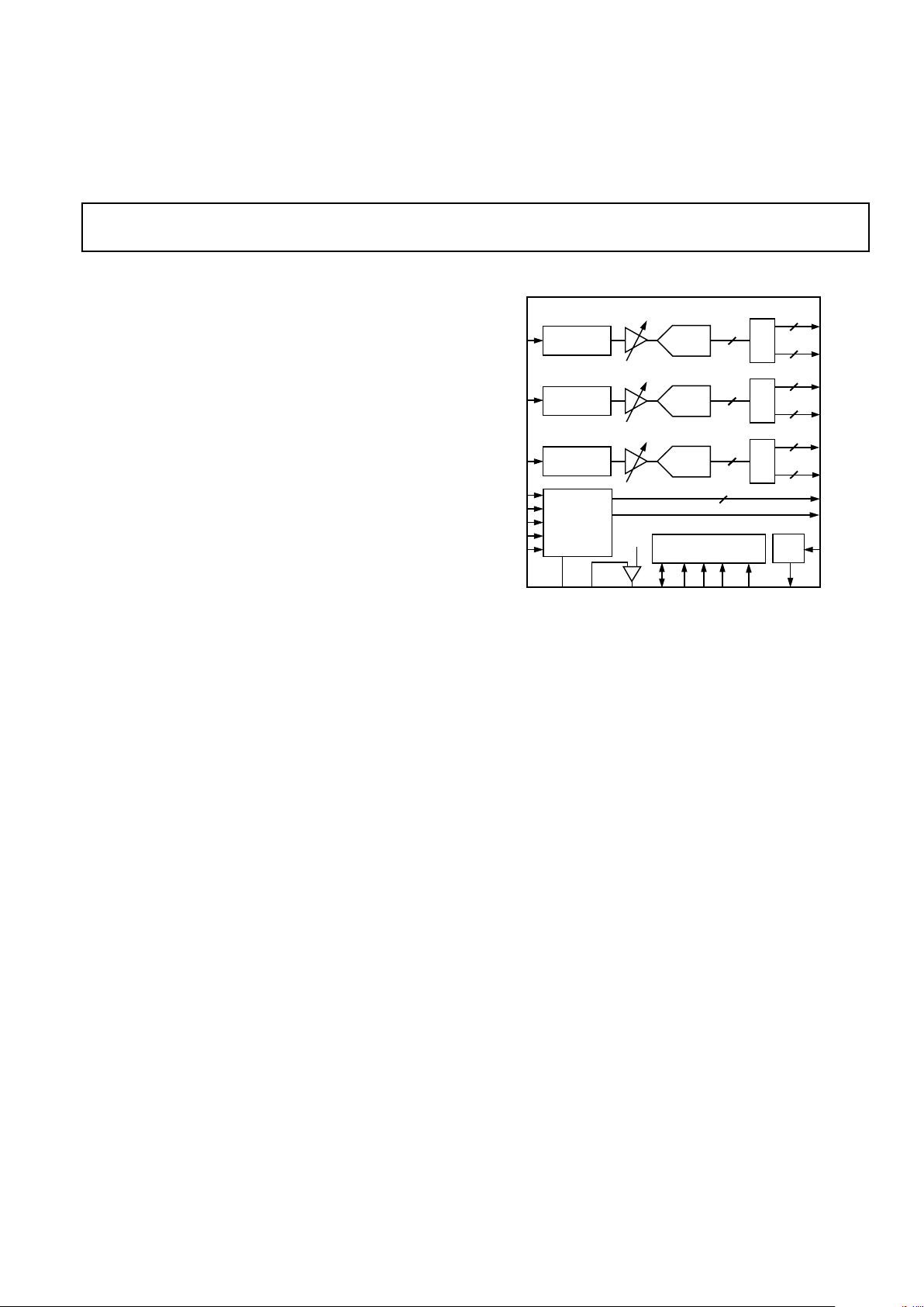
FUNCTIONAL BLOCK DIAGRAM
SDA SCL
A0A
1
PWRDN
HSYNC
COAST
CLAMP
FILT
CKEXT REFIN
CKINV
REFOUT
8
A/D
CLAMP
R
IN
G
IN
B
IN
8
A/D
CLAMP
8
8
A/D
CLAMP
8
REF
8
8
8
8
8
8
SOGIN
0.15V
2
AD9884A
CLOCK
GENERATOR
SOGOUT
DATACK
R
OUTA
R
OUTB
G
OUTA
G
OUTB
B
OUTA
B
OUTB
HSOUT
CONTROL
20 MHz to 140 MHz. PLL clock jitter is typically 400 ps p-p
relative to the input reference. When the COAST signal is presented, the PLL maintains its output frequency in the absence
of HSYNC. A 32-step sampling phase adjustment is provided.
Data, HSYNC and Data Clock output phase relationships are
always maintained. The PLL can be disabled and an external
clock input provided as the pixel clock.
A clamp signal is generated internally or may be provided by the
user through the CLAMP input pin. This device is fully programmable via a two-wire serial port.
Fabricated in an advanced CMOS process, the AD9884A is
provided in a space-saving 128-lead MQFP surface mount plas-
tic package and is specified over a 0°C to +70°C temperature
range.
REV. B–2–
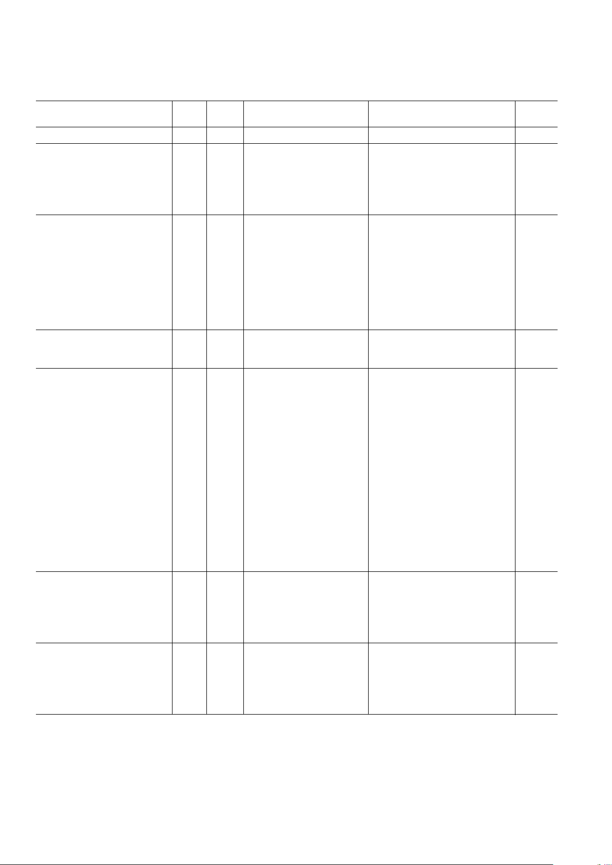
AD9884A–SPECIFICATIONS
(VD = +3.3 V, VDD = +3.3 V, PVD = +3.3 V, ADC Clock Frequency = Maximum, PLL
Clock Frequency = Maximum, Control Registers Programmed to Default State)
Test AD9884AKS-100 AD9884AKS-140
Parameter Temp Level Min Typ Max Min Typ Max Unit
RESOLUTION 8 8 Bits
DC ACCURACY
Differential Nonlinearity +25°CI ±0.5 ±1.0 ±0.5 +1.15/–1.0 LSB
Full VI ±1.0 +1.25/–1.0 LSB
Integral Nonlinearity +25°CI ±0.5 ±1.25 ±0.8 ±1.4 LSB
Full VI ±1.75 ±2.5 LSB
No Missing Codes Full VI Guaranteed Guaranteed
ANALOG INPUT
Input Voltage Range
Minimum Full VI 0.5 0.5 V p-p
Maximum Full VI 1.0 1.0 V p-p
Gain Tempco +25°C V 100 280 ppm/°C
Input Bias Current +25°CI 1 1 µA
Full VI 1 1 µA
Input Offset Voltage Full VI 7 50 7 50 mV
Input Full-Scale Matching Full VI 1.5 5.0 1.5 5.0 %FS
Offset Adjustment Range Full VI 22 23.5 25 22 23.5 25 %FS
REFERENCE OUTPUT
Output Voltage Full VI +1.20 +1.25 +1.30 +1.20 +1.25 +1.30 V
Temperature Coefficient Full V ±50 ±50 ppm/°C
SWITCHING PERFORMANCE
Maximum Conversion Rate Full VI 100 140 MSPS
Minimum Conversion Rate Full IV 10 10 MSPS
Data to Clock Skew, t
SKEW
Full IV –0.5 +2.0 –0.5 +2.0 ns
t
BUFF
Full VI 4.7 4.7 µs
t
STAH
Full VI 4.0 4.0 µs
t
DHO
Full VI 0 0 µs
t
DAL
Full VI 4.7 4.7 µs
t
DAH
Full VI 4.0 4.0 µs
t
DSU
Full VI 250 250 ns
t
STASU
Full VI 4.7 4.7 µs
t
STOSU
Full VI 4.0 4.0 µs
HSYNC Input Frequency Full IV 15 110 15 110 kHz
Maximum PLL Clock Rate Full VI 100 140 MHz
Minimum PLL Clock Rate Full IV 20 20 MHz
PLL Jitter +25°C IV 400 700
1
475 750
2
ps p-p
Full IV 1000
1
1000
2
ps p-p
Sampling Phase Tempco Full IV 15 15 ps/°C
DIGITAL INPUTS
Input Voltage, High (V
IH
) Full VI 2.5 2.5 V
Input Voltage, Low (V
IL
) Full VI 0.8 0.8 V
Input Current, High (I
IH
) Full VI –1.0 –1.0 µA
Input Current, Low (I
IL
) Full VI 1.0 1.0 µA
Input Capacitance +25°CV 3 3 pF
DIGITAL OUTPUTS
Output Voltage, High (V
OH
) Full VI VDD – 0.1 VDD – 0.1 V
Output Voltage, Low (V
OL
) Full VI 0.1 0.1 V
Duty Cycle
DATACK, DATACK Full IV 45 50 55 45 50 55 %
Output Coding Binary Binary
REV. B –3–
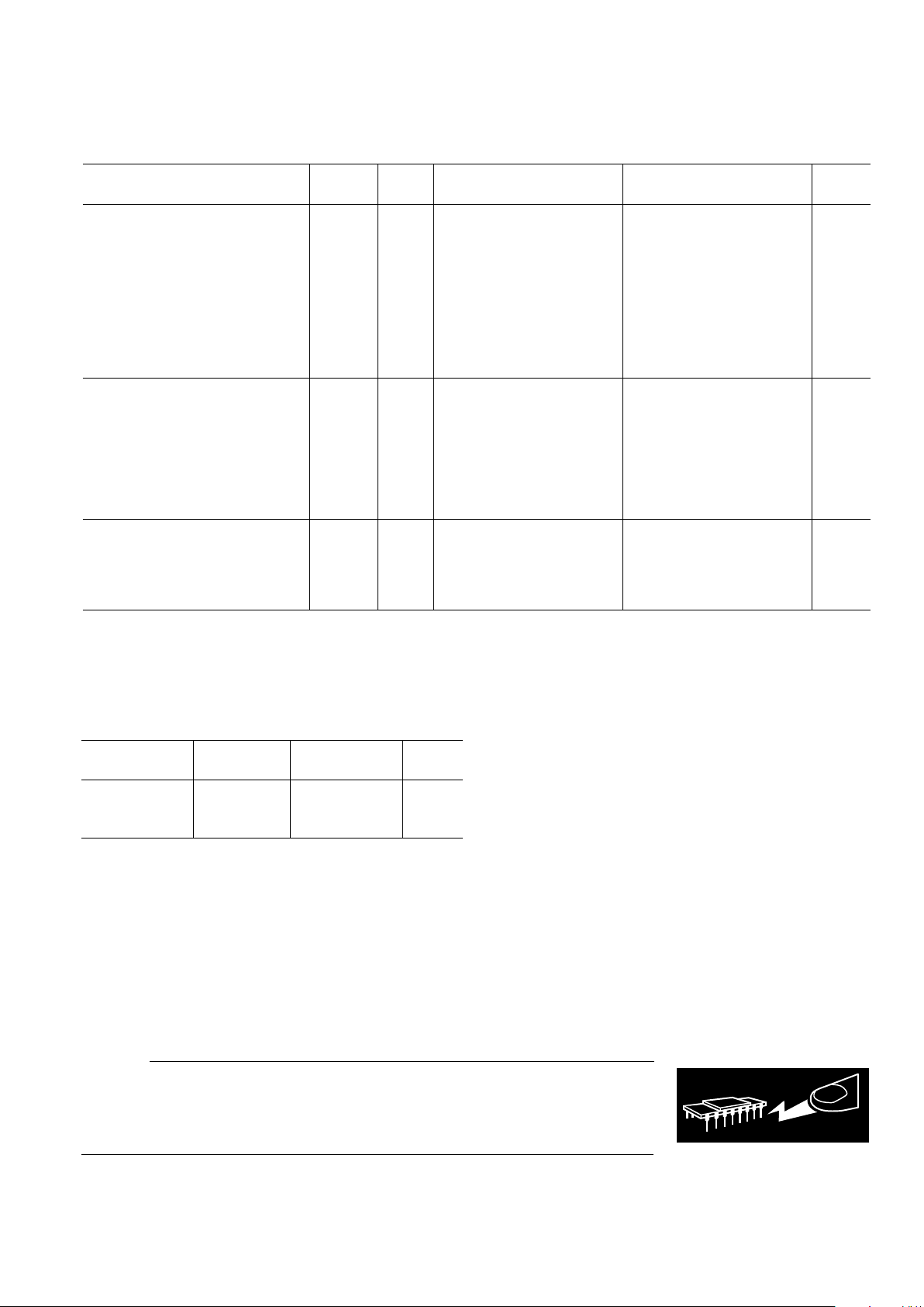
AD9884A
Test AD9884AKS-100 AD9884AKS-140
Parameter Temp Level Min Typ Max Min Typ Max Unit
POWER SUPPLY
V
D
Supply Voltage Full IV 3.0 3.3 3.6 3.0 3.3 3.6 V
V
DD
Supply Voltage Full IV 2.2 3.3 3.6 2.2 3.3 3.6 V
PV
D
Supply Voltage Full IV 3.0 3.3 3.6 3.0 3.3 3.6 V
I
D
Supply Current (V
D
) +25°C V 125 135 mA
I
DD
Supply Current (VDD)
3
+25°C V 33 47 mA
IPV
D
Supply Current (PV
D
) +25°C V 15 15 mA
Total Power Dissipation Full VI 570 675 650 775 mW
Power-Down Supply Current Full VI 2.0 25 2.0 25 mA
Power-Down Dissipation Full VI 6.6 82.5 6.6 82.5 mW
DYNAMIC PERFORMANCE
Analog Bandwidth, Full Power +25°C V 500 500 MHz
Transient Response +25°CV 2 2 ns
Overvoltage Recovery Time +25°C V 1.5 1.5 ns
Signal-to-Noise Ratio (SNR)
4
+25°C I 44.0 46.5 43.5 46.2 dB
(Without Harmonics) Full V 46.0 45.0 dB
f
IN
= 40.7 MHz
Crosstalk Full V 60 60 dBc
THERMAL CHARACTERISTICS
θ
JC
–Junction-to-Case
Thermal Resistance V 8.4 8.4 °C/W
θ
JA
–Junction-to-Ambient
Thermal Resistance V 35 35 °C/W
NOTES
1
VCORNGE = 01, CURRENT = 001, PLLDIV = 169310.
2
VCORNGE = 10, CURRENT = 110, PLLDIV = 160010.
3
DEMUX = 1; DATACK and DATACK load = 15 pF; Data load = 5 pF.
4
Using external pixel clock.
Specifications subject to change without notice.
ORDERING GUIDE
Temperature Package Package
Model Range Description Option
AD9884AKS-140 0°C to +70°C MQFP S-128
AD9884AKS-100 0°C to +70°C MQFP S-128
AD9884A/PCB +25°C Evaluation Board
EXPLANATION OF TEST LEVELS
Test Level
I. 100% production tested.
II. 100% production tested at +25°C and sample tested at specified
temperatures.
III. Sample tested only.
IV. Parameter is guaranteed by design and characterization testing.
V. Parameter is a typical value only.
VI. 100% production tested at +25°C; guaranteed by design and
characterization testing.
ABSOLUTE MAXIMUM RATINGS
*
V
D, PVD
. . . . . . . . . . . . . . . . . . . . . . . . . . . . . . –0.5 V to +4 V
PV
D
to V
D
. . . . . . . . . . . . . . . . . . . . . . . . . . . . . . . . . . ±0.5 V
V
DD
. . . . . . . . . . . . . . . . . . . . . . . . . . . . . . . . . –0.5 V to +4 V
Analog Inputs . . . . . . . . . . . . . . . . . . . . . . . . . . . V
D
to –0.5 V
REFIN . . . . . . . . . . . . . . . . . . . . . . . . . . . . . . . . . . V
D
to 0.0 V
Digital Inputs . . . . . . . . . . . . . . . . . . . . . . . . . . . . V
D
to 0.0 V
Digital Output Current . . . . . . . . . . . . . . . . . . . . . . . . 20 mA
Operating Temperature . . . . . . . . . . . . . . . . . –20°C to +85°C
Storage Temperature . . . . . . . . . . . . . . . . . . –65°C to +150°C
Maximum Junction Temperature . . . . . . . . . . . . . . . +175°C
Maximum Case Temperature . . . . . . . . . . . . . . . . . . +150°C
*Stresses above those listed under Absolute Maximum Ratings may cause perma-
nent damage to the device. This is a stress rating only; functional operation of the
device at these or any other conditions outside of those indicated in the operation
sections of this specification is not implied. Exposure to absolute maximum ratings
for extended periods may affect device reliability.
CAUTION
ESD (electrostatic discharge) sensitive device. Electrostatic charges as high as 4000 V readily
accumulate on the human body and test equipment and can discharge without detection.
Although the AD9884A features proprietary ESD protection circuitry, permanent damage may
occur on devices subjected to high energy electrostatic discharges. Therefore, proper ESD
precautions are recommended to avoid performance degradation or loss of functionality.
WARNING!
ESD SENSITIVE DEVICE
REV. B
AD9884A
–4–
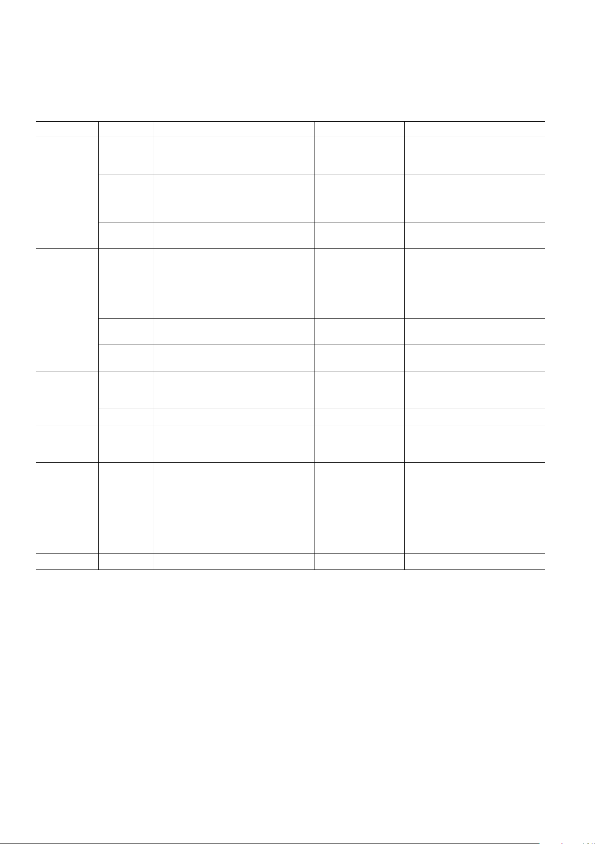
Table I. Package Interconnections
Signal Type Name Function Value Package Pin
Inputs R
AIN
Analog Input for RED Channel 0.5 V to 1.0 V FS 7
G
AIN
Analog Input for GREEN Channel 0.5 V to 1.0 V FS 15
B
AIN
Analog Input for BLUE Channel 0.5 V to 1.0 V FS 22
HSYNC Horizontal Sync Input 3.3 V CMOS 40
COAST Clock Generator Coast Input (Optional) 3.3 V CMOS 41
CLAMP External Clamp Input (Optional) 3.3 V CMOS 28
SOGIN Sync On Green Slicer Input (Optional) 0.5 V to 1.0 V FS 14
CKEXT External Clock Input (Optional) 3.3 V CMOS 44
CKINV Sampling Clock Inversion (Optional) 3.3 V CMOS 27
Outputs D
RA7-0
Data Output, Red Channel, Port A 3.3 V CMOS 105–112
D
RB7-0
Data Output, Red Channel, Port B 3.3 V CMOS 95–102
D
GA7-0
Data Output, Green Channel, Port A 3.3 V CMOS 85–92
D
GB7-0
Data Output, Green Channel, Port B 3.3 V CMOS 75–82
D
BA7-0
Data Output, Blue Channel, Port A 3.3 V CMOS 65–72
DBB
7-0
Data Output, Blue Channel, Port B 3.3 V CMOS 55–62
DATACK Data Output Clock 3.3 V CMOS 115
DATACK Data Output Clock Complement 3.3 V CMOS 116
HSOUT Horizontal Sync Output 3.3 V CMOS 117
SOGOUT Sync On Green Slicer Output 3.3 V CMOS 118
Control SDA Serial Data I/O 3.3 V CMOS 29
SCL Serial Interface Clock 3.3 V CMOS 30
A0, A
1
Serial Port Address LSBs 3.3 V CMOS 31, 32
PWRDN Power-Down Control Input 3.3 V CMOS 125
Analog Interface REFOUT Internal Reference Output +1.25 V 126
REFIN Reference Input +1.25 V ± 10% 127
FILT External Filter Connection 45
Power Supply V
D
Main Power Supply 3.3 V ± 10% 4, 8, 10, 11, 16, 18, 19, 23, 25,
124, 128
V
DD
Digital Output Power Supply 2.5 V to 3.3 V ± 10% 54, 64, 74, 84, 94, 104, 114, 120
PV
D
Clock Generator Power Supply 3.3 V ± 10% 33, 34, 43, 48, 50
GND Ground 0 V 5, 6, 9, 12, 13, 17, 20, 21, 24, 26,
35, 39, 42, 47, 49, 51, 52, 53, 63,
73, 83, 93, 103, 113, 119, 121,
122, 123
No Connect NC 1–3, 36–38, 46
REV. B
AD9884A
–5–
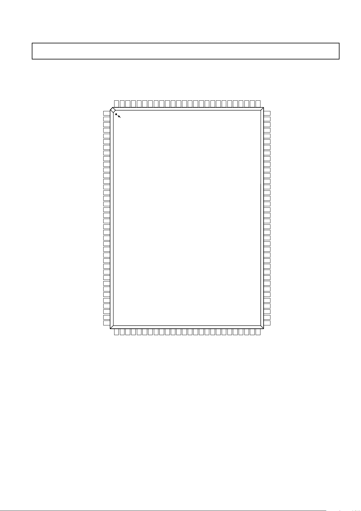
PIN CONFIGURATION
92
93
95
90
91
88
89
87
96
86
94
81
82
83
84
79
80
78
76
77
85
75
73
74
71
72
69
70
67
68
66
65
98
99
101
97
102
100
41
42
43
44
46
47
48
49
39
45
40
62
61
60
64
63
59
55
50
51
52
53
54
56
57
58
11
10
16
15
14
13
18
17
20
19
22
21
12
24
23
26
25
28
27
30
29
32
31
5
4
3
2
7
6
9
8
1
34
33
36
35
38
37
120
121
122
123
124
125
126
127
128
119
111
118
117
116
115
114
113
112
110
109
108
107
106
105
104
103
PIN 1
IDENTIFIER
TOP VIEW
PINS DOWN
(Not to Scale)
V
D
REFIN
REFOUT
PWRDN
V
D
GND
GND
GND
V
DD
GND
SOGOUT
HSOUT
DATACK
DATACK
V
DD
GND
D
R
A
0
D
R
A
1
D
R
A
2
D
R
A
3
HSYNC
COAST
GND
PV
D
CKEXT
FILT
NC
GND
PV
D
GND
PV
D
GND
GND
GND
V
DD
D
B
B
7
D
B
B
6
D
B
B
5
D
B
B
4
DRB
0
DRB
1
DRB
2
DRB
3
DRB
4
DRB
5
DRB
6
DRB
7
V
DD
GND
D
GA0
DGA
1
DGA
2
DGB
2
DGB
3
DGB
4
DGB
5
DGB
6
DGB
7
V
DD
GND
NC
NC
NC
V
D
GND
GND
R
AIN
V
D
GND
V
D
V
D
GND
GND
SOGIN
G
AIN
V
D
GND
V
D
V
D
GND
GND
B
AIN
V
D
GND
V
D
GND
CKINV
CLAMP
SDA
SCL
A
0
A
1
D
B
B
3
D
B
B
2
D
B
B
1
D
B
B
0
GND
V
DD
GND
DBA
0
DBA
1
D
R
A
4
D
R
A
5
D
R
A
6
D
R
A
7
V
DD
GND
DGA
3
DGA
4
DGA
5
DGA
6
DGA
7
V
DD
GND
D
GB0
DGB
1
AD9884A
PV
D
PV
D
GND
NC
NC
NC
D
BA2
DBA
3
DBA
4
DBA
5
DBA
6
DBA
7
NC = NO CONNECT

REV. B
AD9884A
–6–
PIN FUNCTION DESCRIPTIONS
Pin Name Function
INPUTS
R
AIN
Analog Input for RED Channel
G
AIN
Analog Input for GREEN Channel
B
AIN
Analog Input for BLUE Channel
High impedance inputs that accepts the RED, GREEN, and BLUE channel graphics signals, respectively. The
three channels are identical, and can be used for any colors, but colors are assigned for convenient reference. They
accommodate input signals ranging from 0.5 V to 1.0 V full scale. Signals should be ac-coupled to these pins to
support clamp operation.
HSYNC Horizontal Sync Input
This input receives a logic signal that establishes the horizontal timing reference and provides the frequency reference for pixel clock generation. The logic sense of this pin is controlled by HSPOL. Only the leading edge of
HSYNC is active. When HSPOL = 0, the falling edge of HSYNC is used. When HSPOL = 1, the rising edge is
active. The input includes a Schmitt trigger for noise immunity, with a nominal input threshold of 1.5 V.
Electrostatic Discharge (ESD) protection diodes will conduct heavily if this pin is driven more than 0.5 V above
the 3.3 V power supply (or more than 0.5 V below ground). If a 5 V signal source is driving this pin, the signal
should be clamped or current limited.
COAST Clock Generator Coast Input (optional)
This input may be used to cause the pixel clock generator to stop synchronizing with HSYNC and continue producing a clock at its present frequency and phase. This is useful when processing sources that fail to produce horizontal sync pulses when in the vertical interval. The COAST signal is generally NOT required for PC-generated
signals. The logic sense of this pin is controlled by CSTPOL. COAST may be asserted at any time. When not
used, this pin must be grounded and CSTPOL programmed to 1. CSTPOL defaults to 1 at power-up.
CLAMP External Clamp Input (optional)
This logic input may be used to define the time during which the input signal is clamped to ground, establishing a
black reference. It should be exercised when a black signal is known to be present on the analog input channels,
typically during the back porch period of the graphics signal. The CLAMP pin is enabled by setting control bit
EXTCLMP to 1 (default power-up is 0). When disabled, this pin is ignored and the clamp timing is determined
internally by counting a delay and duration from the trailing edge of the HSYNC input. The logic sense of this pin
is controlled by CLAMPOL. When not used, this pin must be grounded and EXTCLMP programmed to 0.
SOGIN Sync On Green Slicer Input (optional)
This input is provided to assist in processing signals with embedded sync, typically on the GREEN channel. The
pin is connected to a high speed comparator with an internally-generated threshold of 0.15 V. When connected to
a dc-coupled graphics signal with embedded sync, it will produce a noninverting digital output on SOGOUT that
changes state whenever the input signal crosses 0.15 V. This is usually a composite sync signal, containing both
vertical and horizontal sync information that must be separated before passing the horizontal sync signal to HSYNC.
The SOG slicer comparator continues to operate when the AD9884A is put into a power-down state. When not
used, this input should be grounded.
CKEXT External Clock Input (optional)
This pin may be used to provide an external clock to the AD9884A, in place of the clock internally-generated from
HSYNC. This input is enabled by programming EXTCLK to 1. When an external clock is used, all other internal
functions operate normally. When unused, this pin should be tied through a 10 kΩ resistor to GROUND, and
EXTCLK programmed to 0. The clock phase adjustment still operates when an external clock source is used.
CKINV Sampling Clock Inversion (optional)
This pin may be used to invert the pixel sampling clock, which has the effect of shifting the sampling phase
180 degrees. This is in support of Alternate Pixel Sampling mode, wherein higher frequency input signals (up to
280 Mpps) may be captured by first sampling the odd pixels, then capturing the even pixels on the subsequent
frame. This pin should be exercised only during blanking intervals (typically vertical blanking) as it may produce
several samples of corrupted data during the phase shift. CKINV should be grounded when not used.
REV. B
AD9884A
–7–
PIN FUNCTION DESCRIPTIONS (Continued)
Pin Name Function
OUTPUTS
DRA
7–0
Data Output, Red Channel, Port A
D
RB7–0
Data Output, Red Channel, Port B
D
GA7–0
Data Output, Green Channel, Port A
D
GB7–0
Data Output, Green Channel, Port B
D
BA7–0
Data Output, Blue Channel, Port A
D
BB7–0
Data Output, Blue Channel, Port B
The main data outputs. Bit 7 is the MSB. Each channel has two ports. When the part is operated in Single Channel mode (DEMUX = 0), all data are presented to Port A, and Port B is placed in a high impedance state. Programming DEMUX to 1 establishes Dual Channel mode, wherein alternate pixels are presented to Port A and
Port B of each channel. These will appear simultaneously, two pixels presented at the time of every second input
pixel, when PAR is set to 1 (parallel mode). When PAR = 0, pixel data appear alternately on the two ports, one
new sample with each incoming pixel (interleaved mode). In Dual Channel mode, the first pixel sampled after
HSYNC is routed to Port A. The second pixel goes to Port B, the third to A, etc. The delay from pixel sampling
time to output is fixed. When the sampling time is changed by adjusting the PHASE register, the output timing is
shifted as well. The DATACK, DATACK and HSOUT outputs are also moved, so the timing relationship among
the signals is maintained.
DATACK Data Output Clock
DATACK Data Output Clock Complement
Differential data clock output signals to be used to strobe the output data and HSOUT into external logic. They
are produced by the internal clock generator and are synchronous with the internal pixel sampling clock. When the
AD9884A is operated in Single Channel mode, the output frequency is equal to the pixel sampling frequency.
When operating in Dual Channel mode, the Data Output Clock and the Output Data are presented at one-half the
pixel rate. When the sampling time is changed by adjusting the PHASE register, the output timing is shifted as
well. The Data, DATACK, DATACK and HSOUT outputs are all moved, so the timing relationship among the
signals is maintained. Either or both signals may be used, depending on the timing mode and interface design
employed.
HSOUT Horizontal Sync Output
A reconstructed and phase-aligned version of the HSYNC input. This signal is always active HIGH. By maintaining alignment with DATACK, DATACK, and Data, data timing with respect to horizontal sync can always be
clearly determined.
SOGOUT Sync On Green Slicer Output
The output of the Sync On Green slicer comparator. When SOGIN is presented with a dc-coupled ground-referenced
analog graphics signal containing composite sync, SOGOUT will produce a digital composite sync signal. This
signal gets no other processing on the AD9884A. The SOG slicer comparator continues to operate when the
AD9884A is put into a power-down state.
CONTROL
SDA Serial Data I/O
Bidirectional data port for the serial interface port.
SCL Serial Interface Clock
Clock input for the serial interface port.
A
1–0
Serial Port Address LSBs
The two least significant bits of the serial port address are set by the logic levels on these pins. Connect a pin to
ground to set the address bit to 0. Tie it HIGH (to V
D
through 10 kΩ) to set the address bit to 1. Using these pins,
the serial address may be set to any value from 98h to 9Fh. Up to four AD9884As may be used on the same serial
bus by appropriately setting these bits. They can also be used to change the AD9884A address if a conflict is found
with another device on the bus.
PWRDN Power-Down Control Input
Bringing this pin LOW puts the AD9884A into a very low power dissipation mode. The output buffers are placed
in a high impedance state. The clock generator is stopped. The control register contents are maintained. The Sync
On Green Slicer (SOGOUT) and internal reference continue to function.

REV. B
AD9884A
–8–
PIN FUNCTION DESCRIPTIONS (Continued)
Pin Name Function
ANALOG INTERFACE
REFOUT Internal Reference Output
Output from the internal 1.25 V bandgap reference. This output is intended to drive relatively light loads. It can
drive the AD9884A Reference input directly, but should be externally buffered if it is used to drive other loads as
well. The absolute accuracy of this output is ±4%, and the temperature coefficient is ±50 ppm, which is adequate
for most AD9884A applications. If higher accuracy is required, an external reference may be employed. If an exter-
nal reference is used, tie this pin to ground through a 0.1 µF capacitor.
REFIN Reference Input
The reference input accepts the master reference voltage for all AD9884A internal circuitry (+1.25 V ± 10%). It
may be driven directly by the REFOUT pin. Its high impedance presents a very light load to the reference source.
This pin should be bypassed to Ground with a 0.1 µF capacitor.
FILT External Filter Connection
For proper operation, the pixel clock generator PLL requires an external filter. Connect the filter shown in Figure
10 to this pin. For optimal performance, minimize noise and parasitics on this node.
POWER SUPPLY
V
D
Main Power Supply
These pins supply power to the main elements of the circuit. It should be as quiet and filtered as possible.
V
DD
Digital Output Power Supply
A large number of output pins (up to 52) switching at high speed (up to 140 MHz) generates a lot of power supply
transients (noise). These supply pins are identified separately from the V
D
pins so special care can be taken to
minimize output noise transferred into the sensitive analog circuitry. If the AD9884A is interfacing with lowervoltage logic, V
DD
may be connected to a lower supply voltage (as low as 2.5 V) for compatibility.
PV
D
Clock Generator Power Supply
The most sensitive portion of the AD9884A is the clock generation circuitry. These pins provide power to the
clock PLL and help the user design for optimal performance. The designer should provide “quiet,” noise-free
power to these pins.
GND Ground
The ground return for all circuitry on chip. It is recommended that the AD9884A be assembled on a single solid
ground plane, with careful attention to ground current paths. See the Design Guide for details.
 Loading...