

Analog Devices AD9883KST-110 Datasheet
REV. 0
Information furnished by Analog Devices is believed to be accurate and
reliable. However, no responsibility is assumed by Analog Devices for its
use, nor for any infringements of patents or other rights of third parties
which may result from its use. No license is granted by implication or
otherwise under any patent or patent rights of Analog Devices.
a
AD9883
One Technology Way, P.O. Box 9106, Norwood, MA 02062-9106, U.S.A.
Tel: 781/329-4700 World Wide Web Site: http://www.analog.com
Fax: 781/326-8703 © Analog Devices, Inc., 2001
110 MSPS Analog Interface for
Flat Panel Displays
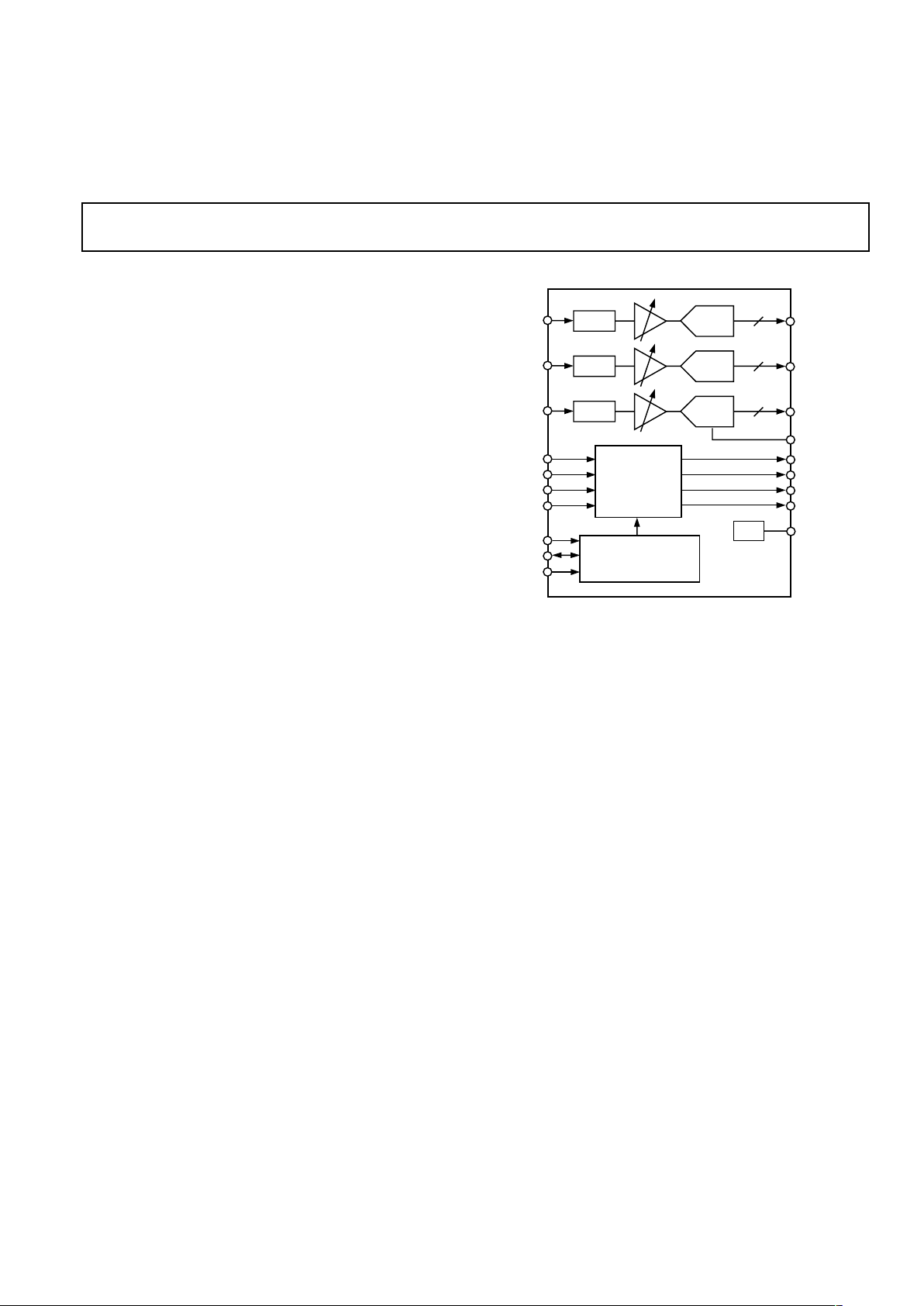
FUNCTIONAL BLOCK DIAGRAM
R
AIN
R
OUTA
G
A
IN
G
OUTA
B
A
IN
B
OUTA
MIDSCV
SYNC
PROCESSING
AND CLOCK
GENERATION
HSYNC
COAST
CLAMP
FILT
DTACK
HSOUT
VSOUT
SOGOUT
REF
REF
BYPASS
SERIAL REGISTER
AND
POWER MANAGEMENT
SCL
SDA
A
0
AD9883
CLAMP
8
A/D
CLAMP
8
A/D
CLAMP
8
A/D
FEATURES
110 MSPS Maximum Conversion Rate
300 MHz Analog Bandwidth
0.5 V to 1.0 V Analog Input Range
500 ps p-p PLL Clock Jitter at 110 MSPS
3.3 V Power Supply
Full Sync Processing
Sync Detect for ”Hot Plugging”
Midscale Clamping
Power-Down Mode
Low Power: 500 mW Typical
Composite Sync Applications Require an External Coast
APPLICATIONS
RGB Graphics Processing
LCD Monitors and Projectors
Plasma Display Panels
Scan Converters
Microdisplays
Digital TV
GENERAL DESCRIPTION
The AD9883 is a complete 8-bit, 110 MSPS monolithic analog
interface optimized for capturing RGB graphics signals from
personal computers and workstations. Its 110 MSPS encode
rate capability and full-power analog bandwidth of 300 MHz
supports resolutions up to SXGA (1280 × 1024 at 60 Hz).
The AD9883 includes a 110 MHz triple ADC with internal
1.25 V reference, a PLL, and programmable gain, offset, and
clamp control. The user provides only a 3.3 V power supply,
analog input, and HSYNC and COAST signals. Three-state
CMOS outputs may be powered from 2.5 V to 3.3 V.
The AD9883’s on-chip PLL generates a pixel clock from HSYNC
and COAST inputs. Pixel clock output frequencies range from
12 MHz to 110 MHz. PLL clock jitter is 500 ps p-p typical at
110 MSPS. When the COAST signal is presented, the PLL
maintains its output frequency in the absence of HSYNC. A
sampling phase adjustment is provided. Data, HSYNC and
Clock output phase relationships are maintained. The AD9883
also offers full sync processing for composite sync and sync-ongreen applications.
A clamp signal is generated internally or may be provided by the
user through the CLAMP input pin. This interface is fully programmable via a two-wire serial interface.
Fabricated in an advanced CMOS process, the AD9883 is
provided in a space-saving 80-lead LQFP surface mount plastic
package and is specified over the 0°C to 70°C temperature range.
REV. 0
–2–
AD9883–SPECIFICATIONS
(VD = 3.3 V, VDD = 3.3 V, ADC Clock = Maximum Conversion Rate)
Analog Interface
Test AD9883KST-110
Parameter Temp Level Min Typ Max Unit
RESOLUTION 8 Bits
DC ACCURACY
Differential Nonlinearity 25°CI ± 0.5 +1.25/–1.0 LSB
Full VI +1.35/–1.0 LSB
Integral Nonlinearity 25°CI ± 0.5 ± 1.85 LSB
Full VI ± 2.0 LSB
No Missing Codes Full VI Guaranteed
ANALOG INPUT
Input Voltage Range
Minimum Full VI 0.5 V p–p
Maximum Full VI 1.0 V p–p
Gain Tempco 25°C V 100 ppm/°C
Input Bias Current 25°CIV 1 µA
Full IV 1 µA
Input Offset Voltage Full VI 7 50 mV
Input Full-Scale Matching Full VI 6.0 % FS
Offset Adjustment Range Full VI 46 49 52 % FS
REFERENCE OUTPUT
Output Voltage Full VI 1.20 1.25 1.32 V
Temperature Coefficient Full V ± 50 ppm/°C
SWITCHING PERFORMANCE
Maximum Conversion Rate Full VI 110 MSPS
Minimum Conversion Rate Full IV 10 MSPS
Data to Clock Skew Full IV –0.5 +2.0 ns
t
BUFF
Full VI 4.7 µs
t
STAH
Full VI 4.0 µs
t
DHO
Full VI 0 µs
t
DAL
Full VI 4.7 µs
t
DAH
Full VI 4.0 µs
t
DSU
Full VI 250 µs
t
STASU
Full VI 4.7 µs
t
STOSU
Full VI 4.0 µs
HSYNC Input Frequency Full IV 15 110 kHz
Maximum PLL Clock Rate Full VI 110 MHz
Minimum PLL Clock Rate Full IV 12 MHz
PLL Jitter 25°C IV 400 700
1
ps p-p
Full IV 1000
1
ps p-p
Sampling Phase Tempco Full IV 15 ps/°C
DIGITAL INPUTS
Input Voltage, High (V
IH
) Full VI 2.5 V
Input Voltage, Low (V
IL
) Full VI 0.8 V
Input Voltage, High (V
IH
) Full V –1.0 µA
Input Voltage, Low (V
IL
) Full V 1.0 µA
Input Capacitance 25°CV 3 pF
DIGITAL OUTPUTS
Output Voltage, High (VOH) Full VI VD– 0.1 V
Output Voltage, Low (V
OL
) Full VI 0.1 V
Duty Cycle DATACK Full IV 45 50 55 %
Output Coding Binary

REV. 0
–3–
AD9883
Test AD9883KST-110
Parameter Temp Level Min Typ Max Unit
POWER SUPPLY
V
D
Supply Voltage Full IV 3.0 3.3 3.6 V
V
DD
Supply Voltage Full IV 2.2 3.3 3.6 V
P
VD
Supply Voltage Full IV 3.0 3.3 3.6 V
I
D
Supply Current (VD)25°C V 132 mA
I
DD
Supply Current (VDD)
2
25°CV 19 mA
IP
VD
Supply Current (PVD)25°CV 8 mA
Total Power Dissipation Full VI 525 650 mW
Power-Down Supply Current Full VI 5 10 mA
Power-Down Dissipation Full VI 16.5 33 mW
DYNAMIC PERFORMANCE
Analog Bandwidth, Full Power 25°C V 300 MHz
Transient Response 25°CV 2 ns
Overvoltage Recovery Time 25°C V 1.5 ns
Signal-to-Noise Ratio (SNR) 25°CV 44 dB
(Without Harmonics) Full V 43 dB
f
IN
= 40.7 MHz
Crosstalk Full V 55 dBc
THERMAL CHARACTERISTICS
θJC Junction-to-Case
Thermal Resistance V 16 °C/W
θ
JA
Junction-to-Ambient
Thermal Resistance V 35 °C/W
NOTES
1
VCO Range = 10, Charge Pump Current = 110, PLL Divider = 1693.
2
DATACK Load = 15 pF, Data Load = 5 pF.
Specifications subject to change without notice.
REV. 0
AD9883
–4–
CAUTION
ESD (electrostatic discharge) sensitive device. Electrostatic charges as high as 4000 V readily
accumulate on the human body and test equipment and can discharge without detection. Although
the AD9883 features proprietary ESD protection circuitry, permanent damage may occur on
devices subjected to high-energy electrostatic discharges. Therefore, proper ESD precautions are
recommended to avoid performance degradation or loss of functionality.
WARNING!
ESD SENSITIVE DEVICE
ABSOLUTE MAXIMUM RATINGS*
VD . . . . . . . . . . . . . . . . . . . . . . . . . . . . . . . . . . . . . . . . . 3.6 V
V
DD
. . . . . . . . . . . . . . . . . . . . . . . . . . . . . . . . . . . . . . . . 3.6 V
Analog Inputs . . . . . . . . . . . . . . . . . . . . . . . . . . . . V
D
to 0.0 V
VREF IN . . . . . . . . . . . . . . . . . . . . . . . . . . . . . . . . V
D
to 0.0 V
Digital Inputs . . . . . . . . . . . . . . . . . . . . . . . . . . . 5 V to 0.0 V
Digital Output Current . . . . . . . . . . . . . . . . . . . . . . . . 20 mA
Operating Temperature . . . . . . . . . . . . . . . . . –25°C to +85°C
Storage Temperature . . . . . . . . . . . . . . . . . . –65°C to +150°C
Maximum Junction Temperature . . . . . . . . . . . . . . . . . 175°C
Maximum Case Temperature . . . . . . . . . . . . . . . . . . . . 150°C
*Stresses above those listed under Absolute Maximum Ratings may cause perma-
nent damage to the device. This is a stress rating only; functional operation of the
device at these or any other conditions outside of those indicated in the operation
sections of this specification is not implied. Exposure to absolute maximum ratings
for extended periods may affect device reliability.
EXPLANATION OF TEST LEVELS
Test Level
I 100% production tested.
II 100% production tested at 25°C and sample tested at
specified temperatures.
III Sample tested only.
IV Parameter is guaranteed by design and characterization testing.
V Parameter is a typical value only.
VI 100% production tested at 25°C; guaranteed by design and
characterization testing.
O
RDERING GUIDE
Temperature Package Package
Model Range Description Option
AD9883KST-110 0°C to 70°C Thin Plastic Quad Flatpack ST-80
AD9883/PCB 25°C Evaluation Board
REV. 0
AD9883
–5–
Table I. Complete Pinout List
Pin Pin
Type Mnemonic Function Value Number
I
nputs R
AIN
Analog Input for Converter R 0.0 V to 1.0 V 54
G
AIN
Analog Input for Converter G 0.0 V to 1.0 V 48
B
AIN
Analog Input for Converter B 0.0 V to 1.0 V 43
HSYNC Horizontal SYNC Input 3.3 V CMOS 30
VSYNC Vertical SYNC Input 3.3 V CMOS 31
SOGIN Input for Sync-on-Green 0.0 V to 1.0 V 49
CLAMP Clamp Input (External CLAMP Signal) 3.3 V CMOS 38
COAST PLL COAST Signal Input 3.3 V CMOS 29
Outputs Red [7:0] Outputs of Converter “Red,” Bit 7 Is the MSB 3.3 V CMOS 70–77
Green [7:0] Outputs of Converter “Green,” Bit 7 Is the MSB 3.3 V CMOS 2–9
Blue [7:0] Outputs of Converter “Blue,” Bit 7 Is the MSB 3.3 V CMOS 12–19
DATACK Data Output Clock 3.3 V CMOS 67
HSOUT HSYNC Output Clock (Phase-Aligned with DATACK) 3.3 V CMOS 66
VSOUT VSYNC Output Clock (Phase-Aligned with DATACK) 3.3 V CMOS 64
SOGOUT Sync on Green Slicer Output 3.3 V CMOS 65
References REF BYPASS Internal Reference Bypass 1.25 V ± 10% 58
MIDSCV Internal Midscale Voltage Bypass 37
FILT Connection for External Filter Components for Internal PLL 33
Power Supply V
D
Analog Power Supply 3.3 V ± 10%
V
DD
Output Power Supply 3.3 V ± 10%
PV
D
PLL Power Supply 3.3 V ± 10%
GND Ground 0 V
Control SDA Serial Port Data I/O 3.3 V CMOS 57
SCL Serial Port Data Clock (100 kHz Maximum) 3.3 V CMOS 56
A0 Serial Port Address Input 1 3.3 V CMOS 55
PIN CONFIGURATION
GND
GREEN <7>
GREEN <6>
GREEN <5>
GREEN <4>
GREEN <3>
GREEN <2>
GREEN <1>
GREEN <0>
GND
VDD
BLUE <7>
BLUE <6>
BLUE <5>
BLUE <4>
BLUE <3>
BLUE <2>
BLUE <1>
BLUE <0>
GND
GND
GND
GND
GND
GND
GND
VD
VD
VD
VD
VD
VD
REF BYPASS
SDA
SCL
A0
R
AIN
G
AIN
B
AIN
SOGIN
80 79 78 77 76 71 70 69 68 67 66 6575 74 73 72 64 63 62 61
1
2
3
4
5
6
7
8
9
10
11
13
14
15
16
12
17
18
20
19
21 22 23 24 25 26 27 28 29 30 31 32 33 34 35 36 37 38 39 40
PIN 1
IDENTIFIER
TOP VIEW
(Not to Scale)
AD9883
60
59
58
57
56
55
54
53
52
51
50
49
48
47
46
45
44
43
42
41
NC = NO CONNECT
GND
VDD
VDD
RED <0>
RED <1>
RED <2>
RED <3>
RED <4>
RED <5>
RED <6>
RED <7>
VDD
GND
DATACK
HSOUT
SOGOUT
GNDVDGND
VSOUT
GND
VDD
VDD
GND
GND
VD
PVD
GND
MIDSCV
CLAMP
VD
GND
COAST
HSYNC
VSYNC
GND
FILT
PVD
VD
GND

REV. 0
AD9883
–6–
PIN FUNCTION DETAIL
Outputs
HSOUT Horizontal Sync Output
A reconstructed and phase-aligned version of
the Hsync input. Both the polarity and duration of this output can be programmed via
serial bus registers.
By maintaining alignment with DATACK,
and Data, data timing with respect to horizontal sync can always be determined.
VSOUT Vertical Sync Output
A reconstructed and phase-aligned version of
the video Vsync. The polarity of this output
can be controlled via a serial bus bit. The placement and duration in all modes is set by the
graphics transmitter.
SOGOUT Sync On Green Slicer Output
This pin outputs either the signal from the
Sync-On-Green slicer comparator or an unprocessed but delayed version of the Hsync input.
See the Sync Block Diagram (Figure 11) to
view how this pin is connected.
(Note: Besides slicing off SOG, the output from
this pin gets no other additional processing on
the AD9883. Vsync separation is performed via
the sync separator.)
Serial Port
(Two-Wire)
SDA Serial Port Data I/O
SCL Serial Port Data Clock
A0 Serial Port Address Input 1
For a full description of the two-wire serial
register and how it works, refer to the TwoWire Serial Control Port section.
Data Outputs
RED Data Output, Red Channel
GREEN Data Output, Green Channel
BLUE Data Output, Blue Channel
The main data outputs. Bit 7 is the MSB. The
delay from pixel sampling time to output is
fixed. When the sampling time is changed by
adjusting the PHASE register, the output timing
is shifted as well. The DATACK and HSOUT
outputs are also moved, so the timing relationship among the signals is maintained. For
exact timing information, refer to Figures 7
and 8.
Data Clock
Output
DATACK Data Output Clock
This is the main clock output signal used to
strobe the output data and HSOUT into
external logic.
It is produced by the internal clock generator
and is synchronous with the internal pixel
sampling clock.
When the sampling time is changed by adjusting the PHASE register, the output timing is
shifted as well. The Data, DATACK, and
HSOUT outputs are all moved, so the timing
relationship among the signals is maintained.
Inputs
R
AIN
Analog Input for RED Channel
G
AIN
Analog Input for GREEN Channel
B
AIN
Analog Input for BLUE Channel
High-impedance inputs that accept the RED,
GREEN, and BLUE channel graphics signals,
respectively. (The three channels are identical,
and can be used for any colors, but colors are
assigned for convenient reference.)
They accommodate input signals ranging from
0.5 V to 1.0 V full scale. Signals should be
ac-coupled to these pins to support clamp
operation.
HSYNC Horizontal Sync Input
This input receives a logic signal that establishes the horizontal timing reference and
provides the frequency reference for pixel
clock generation.
The logic sense of this pin is controlled by
serial register 0Eh Bit 6 (Hsync Polarity). Only
the leading edge of Hsync is active, the trailing
edge is ignored. When Hsync Polarity = 0, the
falling edge of Hsync is used. When Hsync
Polarity = 1, the rising edge is active.
The input includes a Schmitt trigger for noise
immunity, with a nominal input threshold
of 1.5 V.
VSYNC Vertical Sync Input
This is the input for vertical sync.
SOGIN Sync-on-Green Input
This input is provided to assist with processing
signals with embedded sync, typically on the
GREEN channel. The pin is connected to a
high-speed comparator with an internally generated threshold. The threshold level can be
programmed in 10 mV steps to any voltage
between 10 mV and 330 mV above the negative
peak of the input signal. The default voltage
threshold is 150 mV.
When connected to an ac-coupled graphics
signal with embedded sync, it will produce
a noninverting digital output on SOGOUT.
(This is usually a composite sync signal, containing both vertical and horizontal sync information
that must be separated before passing the horizontal sync signal to Hsync.)
When not used, this input should be left unconnected. For more details on this function and
how it should be configured, refer to the Sync
on Green section.

REV. 0
AD9883
–7–
CLAMP External Clamp Input
This logic input may be used to define the
time during which the input signal is clamped
to ground. It should be exercised when the
reference dc level is known to be present on
the analog input channels, typically during the
back porch of the graphics signal. The CLAMP
pin is enabled by setting control bit Clamp
Function to 1, (register 0FH, Bit 7, default is
0). When disabled, this pin is ignored and the
clamp timing is determined internally by counting a delay and duration from the trailing edge
of the HSYNC input. The logic sense of this pin
is controlled by Clamp Polarity register 0FH,
Bit 6. When not used, this pin must be grounded
and Clamp Function programmed to 0.
COAST Clock Generator Coast Input (Optional)
This input may be used to cause the pixel
clock generator to stop synchronizing with
Hsync and continue producing a clock at its
current frequency and phase. This is useful
when processing signals from sources that fail
to produce horizontal sync pulses during the
vertical interval. The COAST signal is generally NOT required for PC-generated signals.
The logic sense of this pin is controlled by
Coast Polarity, (register 0FH, Bit 3).
When not used, this pin may be grounded
and Coast Polarity programmed to 1, or tied
HIGH (to V
D
through a 10 kΩ resistor) and
Coast Polarity programmed to 0. Coast
Polarity defaults to 1 at power-up.
REF BYPASS Internal Reference BYPASS
Bypass for the internal 1.25 V bandgap reference. It should be connected to ground
through a 0.1 µF capacitor.
The absolute accuracy of this reference is ±4%,
and the temperature coefficient is ± 50 ppm,
which is adequate for most AD9883 applications. If higher accuracy is required, an external
reference may be employed instead.
MIDSCV Midscale Voltage Reference BYPASS
Bypass for the internal midscale voltage reference. It should be connected to ground through
a 0.1 µF capacitor. The exact voltage varies
with the gain setting of the BLUE channel.
FILT External Filter Connection
For proper operation, the pixel clock generator
PLL requires an external filter. Connect the
filter shown in Figure 6 to this pin. For optimal
performance, minimize noise and parasitics on
this node.
Power Supply
V
D
Main Power Supply
These pins supply power to the main elements
of the circuit. They should be as quiet and
filtered as possible.
V
DD
Digital Output Power Supply
A large number of output pins (up to 25)
switching at high speed (up to 110 MHz)
generates a lot of power supply transients
(noise). These supply pins are identified separately from the V
D
pins so special care can be
taken to minimize output noise transferred
into the sensitive analog circuitry.
If the AD9883 is interfacing with lower-voltage
logic, V
DD
may be connected to a lower supply
voltage (as low as 2.5 V) for compatibility.
PV
D
Clock Generator Power Supply
The most sensitive portion of the AD9883 is
the clock generation circuitry. These pins
provide power to the clock PLL and help the
user design for optimal performance. The
designer should provide “quiet,” noise-free
power to these pins.
GND Ground
The ground return for all circuitry on chip. It
is recommended that the AD9883 be assembled
on a single solid ground plane, with careful
attention to ground current paths.
DESIGN GUIDE
General Description
The AD9883 is a fully integrated solution for capturing analog
RGB signals and digitizing them for display on flat panel monitors or projectors. The circuit is ideal for providing a computer
interface for HDTV monitors or as the front-end to highperformance video scan converters.
Implemented in a high-performance CMOS process, the interface can capture signals with pixel rates of up to 110 MHz.
The AD9883 includes all necessary input buffering, signal dc
restoration (clamping), offset and gain (brightness and contrast)
adjustment, pixel clock generation, sampling phase control, and
output data formatting. All controls are programmable via a
2-wire serial interface. Full integration of these sensitive analog
functions makes system design straightforward and less sensitive
to the physical and electrical environment.
With a typical power dissipation of only 500 mW and an operating temperature range of 0°C to 70°C, the device requires no
special environmental considerations.
Digital Inputs
All digital inputs on the AD9883 operate to 3.3 V CMOS levels.
However, all digital inputs are 5 V tolerant. (Applying 5 V to
them will not cause any damage.)
Input Signal Handling
The AD9883 has three high-impedance analog input pins for
the Red, Green, and Blue channels. They will accommodate
signals ranging from 0.5 V to 1.0 V p-p.
Signals are typically brought onto the interface board via a
DVI-I connector, a 15-pin D connector, or via BNC connectors.
The AD9883 should be located as close as practical to the input
connector. Signals should be routed via matched-impedance
traces (normally 75 Ω) to the IC input pins.
REV. 0
AD9883
–8–
At that point the signal should be resistively terminated (75 Ω to
the signal ground return) and capacitively coupled to the AD9883
inputs through 47 nF capacitors. These capacitors form part of
the dc restoration circuit.
In an ideal world of perfectly matched impedances, the best performance can be obtained with the widest possible signal bandwidth.
The ultrawide bandwidth inputs of the AD9883 (300 MHz) can
track the input signal continuously as it moves from one pixel level
to the next, and digitize the pixel during a long, flat pixel time. In
many systems, however, there are mismatches, reflections, and
noise, which can result in excessive ringing and distortion of the
input waveform. This makes it more difficult to establish a sampling phase that provides good image quality. It has been shown
that a small inductor in series with the input is effective in
rolling off the input bandwidth slightly, and providing a high
quality signal over a wider range of conditions. Using a FairRite #2508051217Z0- High-Speed Signal Chip Bead inductor
in the circuit of Figure 1 gives good results in most applications.
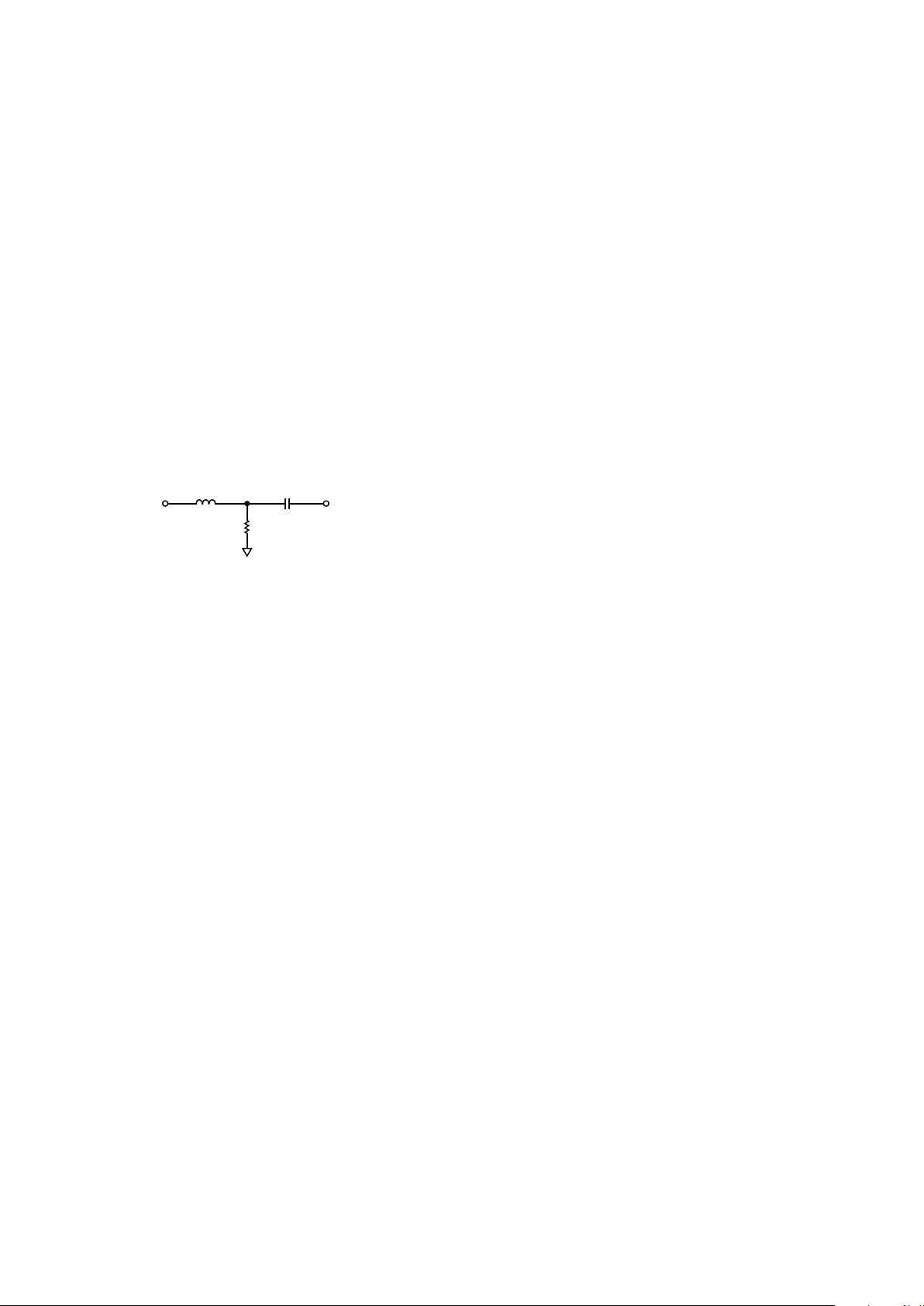
RGB
INPUT
R
AIN
G
AIN
B
AIN
47nF
75⍀
Figure 1. Analog Input Interface Circuit
Hsync, Vsync Inputs
The interface also takes a horizontal sync signal, which is used
to generate the pixel clock and clamp timing. This can be either
a sync signal directly from the graphics source, or a preprocessed
TTL or CMOS level signal.
The Hsync input includes a Schmitt trigger buffer for immunity
to noise and signals with long rise times. In typical PC-based
graphic systems, the sync signals are simply TTL-level drivers
feeding unshielded wires in the monitor cable. As such, no termination is required.
Serial Control Port
The serial control port is designed for 3.3 V logic. If there are 5 V
drivers on the bus, these pins should be protected with 150 Ω series
resistors placed between the pull-up resistors and the input pins.
Output Signal Handling
The digital outputs are designed and specified to operate from a
3.3 V power supply (V
DD
). They can also work with a VDD as
low as 2.5 V for compatibility with other 2.5 V logic.
Clamping
RGB Clamping
To properly digitize the incoming signal, the dc offset of the input
must be adjusted to fit the range of the on-board A/D converters.
Most graphics systems produce RGB signals with black at
ground and white at approximately 0.75 V. However, if sync
signals are embedded in the graphics, the sync tip is often at
ground and black is at 300 mV. Then white is at approximately
1.0 V. Some common RGB line amplifier boxes use emitterfollower buffers to split signals and increase drive capability.
This introduces a 700 mV dc offset to the signal, which must be
removed for proper capture by the AD9883.
The key to clamping is to identify a portion (time) of the signal
when the graphic system is known to be producing black. An
offset is then introduced which results in the A/D converters
producing a black output (code 00h) when the known black
input is present. The offset then remains in place when other
signal levels are processed, and the entire signal is shifted to eliminate offset errors.
In most pc graphics systems, black is transmitted between active
video lines. With CRT displays, when the electron beam has
completed writing a horizontal line on the screen (at the right
side), the beam is deflected quickly to the left side of the screen
(called horizontal retrace) and a black signal is provided to
prevent the beam from disturbing the image.
In systems with embedded sync, a blacker-than-black signal
(Hsync) is produced briefly to signal the CRT that it is time to
begin a retrace. For obvious reasons, it is important to avoid
clamping on the tip of Hsync. Fortunately, there is virtually
always a period following Hsync called the back porch where a
good black reference is provided. This is the time when clamping should be done.
The clamp timing can be established by simply exercising the
CLAMP pin at the appropriate time (with External Clamp = 1).
The polarity of this signal is set by the Clamp Polarity bit.
A simpler method of clamp timing employs the AD9883 internal
clamp timing generator. The Clamp Placement register is programmed with the number of pixel times that should pass after
the trailing edge of HSYNC before clamping starts. A second
register (Clamp Duration) sets the duration of the clamp.
These are both 8-bit values, providing considerable flexibility in
clamp generation. The clamp timing is referenced to the trailing
edge of Hsync because, though Hsync duration can vary widely,
the back porch (black reference) always follows Hsync. A good
starting point for establishing clamping is to set the clamp placement to 09h (providing 9 pixel periods for the graphics signal to
stabilize after sync) and set the clamp duration to 14h (giving
the clamp 20 pixel periods to reestablish the black reference).
Clamping is accomplished by placing an appropriate charge on
the external input coupling capacitor. The value of this capacitor affects the performance of the clamp. If it is too small, there
will be a significant amplitude change during a horizontal line
time (between clamping intervals). If the capacitor is too large,
then it will take excessively long for the clamp to recover from a
large change in incoming signal offset. The recommended value
(47 nF) results in recovering from a step error of 100 mV to
within 1/2 LSB in 10 lines with a clamp duration of 20 pixel
periods on a 60 Hz SXGA signal.
YUV Clamping
YUV graphic signals are slightly different from RGB signals in
that the dc reference level (black level in RGB signals) can be at
the midpoint of the graphics signal rather than the bottom. For
these signals it can be necessary to clamp to the midscale range
of the A/D converter range (80h) rather than bottom of the A/D
converter range (00h).
Clamping to midscale rather than ground can be accomplished
by setting the clamp select bits in the serial bus register. Each of
the three converters has its own selection bit so that they can be
clamped to either midscale or ground independently. These bits
are located in register 10h and are Bits 0–2. The midscale reference voltage that each A/D converter clamps to is provided on
the MIDSCV pin, (Pin 37). This pin should be bypassed to
ground with a 0.1 µF capacitor, (even if midscale clamping is
not required).
 Loading...