Mixed-Signal Front End
FEATURES
Low cost 3.3 V MxFE™ for
DOCSIS-, EURO-DOCSIS-, DVB-, DAVIC-compliant
set-top box and cable modem applications
232 MHz quadrature digital upconverter
12-bit direct IF DAC (TxDAC+™)
Up to 65 MHz carrier frequency DDS
Programmable sampling clock rates
16× upsampling interpolation LPF
Single-tone frequency synthesis
Analog Tx output level adjust
Direct cable amp interface
12-bit, 33 MSPS direct IF ADC
with optional video clamping input
10-bit, 33 MSPS direct IF ADC
Dual 7-bit, 16.5 MSPS sampling I/Q ADC
12-bit Σ-∆ auxiliary DAC
APPLICATIONS
Cable modem and satellite systems
Set-top boxes
Power line modem
PC multimedia
Digital communications
Data and video modems
QAM, OFDM, FSK modulation
GENERAL DESCRIPTION
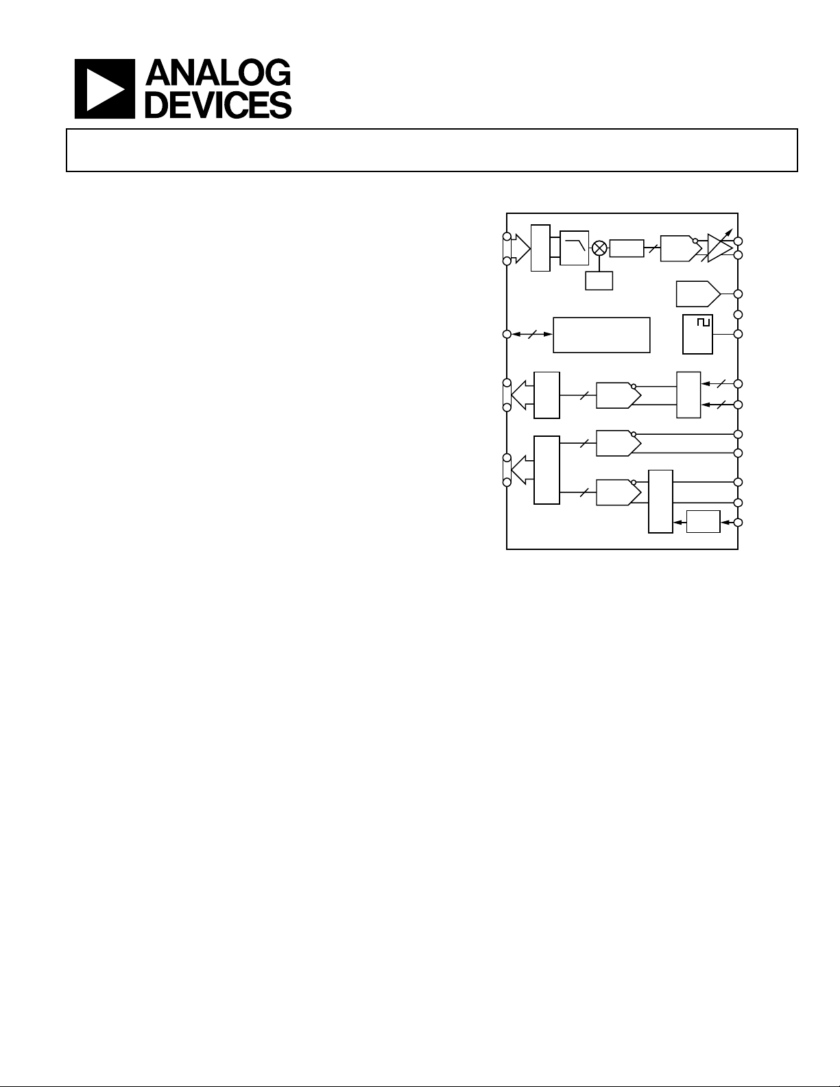
The AD9879 is a single-supply set-top box and cable modem
mixed-signal front end. The device contains a transmit path
interpolation filter, complete quadrature digital upconverter,
and transmit DAC. The receive path contains a 12-bit ADC, a
10-bit ADC, and dual 7-bit ADCs. All internally required clocks
and an output system clock are generated by the phase-locked
loop (PLL) from a single crystal or clock input.
The transmit path interpolation filter provides an upsampling
factor of 16× with an output signal bandwidth as high as
8.3 MHz. Carrier frequencies up to 65 MHz with 26 bits of
frequency tuning resolution can be generated by the direct
digital synthesizer (DDS). The transmit DAC resolution is
12 bits and can run at sampling rates as high as 232 MSPS.
Analog output scaling from 0.0 dB to 7.5 dB in 0.5 dB steps is
available to preserve SNR when reduced output levels are
required.
Set-Top Box, Cable Modem
AD9879
FUNCTIONAL BLOCK DIAGRAM
I
TX DATA
SPORT
RXIQ[3:0]
RXIF[11:0]
TX
Q
4
CONTROL REGISTERS
MUX
MUX
AD9879
⇑16
DDS
8
10
12
Figure 1.
The 12-bit and 10-bit IF ADCs can convert direct IF inputs up
to 70 MHz and run at sample rates up to 33 MSPS. A video
input with an adjustable signal clamping level, along with the
10-bit ADC, allow the AD9879 to process an NTSC and a QAM
channel simultaneously.
The programmable Σ-Δ DAC can be used to control external
components, such as variable gain amplifiers (VGAs) or voltage
controlled tuners. The CA port provides an interface to the
AD8321/AD8323 or AD8322/AD8327 programmable gain
amplifier (PGA) cable drivers, enabling host processor control
via the MxFE SPORT.
The AD9879 is available in a 100-lead MQFP. It offers enhanced
receive path undersampling performance and lower cost when
compared with the pin-compatible AD9873. The AD9879 is
specified over the commercial (−40°C to +85°C) temperature
range.
SINC
ADC
ADC
12
–1
DAC
Σ-∆
PLL
XM/N
MUXADC
MUX
CLAMP
TX
Σ-∆_OUT
CA_PORT
MCLK
2
RXI
2
RXQ
RX10
RX12
VIDEO
02773-001
Rev. A
Information furnished by Analog Devices is believed to be accurate and reliable.
However, no responsibility is assumed by Analog Devices for its use, nor for any
infringements of patents or other rights of third parties that may result from its use.
Specifications subject to change without notice. No license is granted by implication
or otherwise under any patent or patent rights of Analog Devices. Trademarks and
registered trademarks are the property of their respective owners.
One Technology Way, P.O. Box 9106, Norwood, MA 02062-9106, U.S.A.
Tel: 781.329.4700
Fax: 781.461.3113 © 2005 Analog Devices, Inc. All rights reserved.
www.analog.com

AD9879
TABLE OF CONTENTS
Specifications..................................................................................... 4
Serial Interface for Register Control............................................ 20
Absolute Maximum Ratings............................................................ 7
Explanation of Test Levels........................................................... 7
Thermal Characteristics .............................................................. 7
ESD Caution.................................................................................. 7
Pin Configuration and Function Descriptions............................. 8
Te r mi n ol o g y .................................................................................... 10
Theory of Operation ...................................................................... 11
Transmit P at h ..............................................................................11
Data Assembler........................................................................... 11
Interpolation Filter ..................................................................... 12
Digital Upconverter.................................................................... 12
DPLL-A Clock Distribution...................................................... 12
Clock and Oscillator Circuitry ................................................. 12
Programmable Clock Output REFCLK................................... 13
Reset and Transmit Power-Down ............................................ 14
Σ-Δ Outputs ................................................................................15
Register Map and Bit Definitions................................................. 16
Register 0x00—Initialization .................................................... 17
Register 0x01—Clock Configuration....................................... 17
Register 0x02—Power-Down.................................................... 17
Registers 0x03–0x04—Σ-Δ and Flag Control......................... 17
Register 0x07—Video Input Configuration............................ 17
Register 0x08—ADC Clock Configuration ............................ 18
Register 0x0C—Die Revision.................................................... 18
Register 0x0D—Tx Frequency Tuning Words LSBs.............. 18
Register 0x0E—DAC Gain Control .........................................18
Register 0x0F—Tx Path Configuration................................... 18
General Operation of the Serial Interface............................... 20
Instruction Byte .......................................................................... 20
Serial Interface Port Pin Description....................................... 20
MSB/LSB Transfers .................................................................... 20
Notes on Serial Port Operation ................................................ 21
Transmit P at h (Tx) ......................................................................... 22
Transmit T i ming ......................................................................... 22
Data Assembler........................................................................... 22
Half-Band Filters (HBFs).......................................................... 22
Cascaded Integrator-Comb (CIC) Filter................................. 22
Combined Filter Response........................................................ 22
Tx Signal Level Considerations................................................ 24
Tx Throughput and Latency..................................................... 24
Digital-to-Analog Converter .................................................... 25
Programming the AD8321/AD8323 or AD8322/AD8327 Cable
Driver Amplifier Gain Control
Receive Path (Rx) ........................................................................... 27
IF10 and IF12 ADC Operation ................................................ 27
Input Signal Range and Digital Output Codes....................... 27
Driving the Inputs...................................................................... 27
PCB Design Considerations.......................................................... 28
Component Placement.............................................................. 28
Power Planes and Decoupling .................................................. 28
Ground Planes ............................................................................ 29
Signal Routing............................................................................. 29
Outline Dimensions ....................................................................... 30
Ordering Guide .......................................................................... 30
..................................................... 26
Registers 0x10–0x17—Carrier Frequency Tuning................. 19
Rev. A | Page 2 of 32

AD9879
REVISION HISTORY
6/05—Rev. 0 to Rev. A
Updated Format.................................................................. Universal
Changed OSCOUT to REFCLK....................................... Universal
Changed REF CLK to REFCLK........................................ Universal
Changes to Specifications Section................................................... 4
Changes to Figure 13 ......................................................................21
Changes to Equation 18..................................................................24
Changes to Equation 21..................................................................24
Changes to Outline Dimensions................................................... 30
Changes to Ordering Guide........................................................... 30
8/02—Revision 0: Initial Version
Rev. A | Page 3 of 32

AD9879
SPECIFICATIONS
VAS = 3.3 V ± 5%, VDS = 3.3 V ± 10%, f
= 4.02 kΩ, 75 Ω DAC load, unless otherwise noted.
R
SET
Table 1.
Parameter Temp Test Level Min Typ Max Unit
OSCIN AND XTAL CHARACTERISTICS
Frequency Range Full II 3 29 MHz
Duty Cycle Full II 35 50 65 %
Input Impedance 25°C III 100||3 MΩ||pF
MCLK Cycle to Cycle Jitter 25°C III 6 ps rms
Tx DAC CHARACTERISTICS
Resolution N/A N/A 12 Bits
Maximum Sample Rate Full II 232 MHz
Full-Scale Output Current Full II 4 10 20 mA
Gain Error (Using Internal Reference) 25°C I −2.0 −1.0 +2.0 % FS
Offset Error 25°C I ±1.0 % FS
Reference Voltage (REFIO Level) 25°C I 1.18 1.23 1.28 V
Differential Nonlinearity (DNL) 25°C III ±2.5 LSB
Integral Nonlinearity (INL) 25°C III ±8 LSB
Output Capacitance 25°C III 5 pF
Phase Noise @ 1 kHz Offset, 42 MHz
Crystal and OSCIN Multiplier Enabled at 16× 25°C III −110 dBc/Hz
Output Voltage Compliance Range Full II −0.5 +1.5 V
Wideband SFDR
5 MHz Analog Out, I
65 MHz Analog Out, I
= 10 mA Full III 60.8 66.9 dBc
OUT
= 10 mA Full III 44.0 46.2 dBc
OUT
Narrow-band SFDR (±1 MHz Window)
5 MHz Analog Out, I
= 10 mA Full III 65.4 72.3 dBc
OUT
Tx MODULATOR CHARACTERISTICS
I/Q Offset Full II 50 55 dB
Pass-Band Amplitude Ripple (f < f
Pass-Band Amplitude Ripple (f < f
Stop-Band Response (f > f
IQCLK
IQCLK
× 3/4) Full II −63 dB
IQCLK
Tx GAIN CONTROL
Gain Step Size 25°C III 0.5 dB
Gain Step Error 25°C III <0.05 dB
Settling Time to 1% (Full-Scale Step) 25°C III 1.8 µs
IQ ADC CHARACTERISTICS
Resolution
1
Maximum Conversion Rate Full II 14.5 MHz
Pipeline Delay N/A N/A 3.5 ADC cycles
Offset Matching Between I and Q ADCs Full III ±4.0 LSBs
Gain Matching Between I and Q ADCs Full III ±2.0 LSBs
Analog Input
Input Voltage Range
1
Full III 1 Vppd
Input Capacitance 25°C III 2.0 pF
Differential Input Resistance 25°C III 4 kΩ
AC Performance (AIN = 0.5 dBFS, fIN = 5 MHz)
Effective Number of Bits (ENOB) 25°C I 5.00 5.8 Bits
Signal-to-Noise Ratio (SNR) 25°C I 34.7 36.5 dB
Total Harmonic Distortion (THD) 25°C I −50 −36.2 dB
Spurious-Free Dynamic Range (SFDR) 25°C I 41.3 51 dB
= 27 MHz, f
OSCIN
= 216 MHz, f
SYSCLK
= 54 MHz (M = 8), ADC clock from OSCIN,
MCLK
/8) Full II ±0.1 dB
/4) Full II ±0.5 dB
N/A N/A 6 Bits
Rev. A | Page 4 of 32
AD9879
Parameter Temp Test Level Min Typ Max Unit
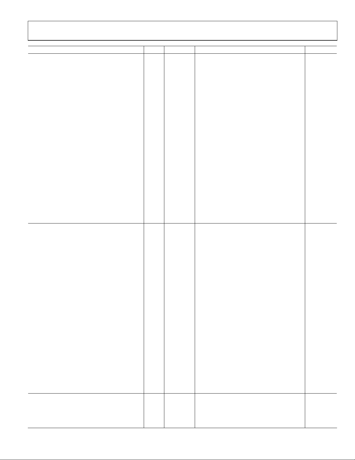
10-BIT ADC CHARACTERISTICS
Resolution N/A N/A 10 Bits
Maximum Conversion Rate Full II 29 MHz
Pipeline Delay N/A N/A 4.5 ADC cycles
Analog Input
Input Voltage Range Full III 2.0 Vppd
Input Capacitance 25°C III 2 pF
Differential Input Resistance 25°C II 4 kΩ
Reference Voltage Error
(REFT10–REFB10) –1 V Full I ±4 ±200 mV
AC Performance (AIN = –0.5 dBFS, fIN = 5 MHz)
ADC Sample Clock Source = OSCIN
Signal-to-Noise and Distortion (SINAD) Full II 58.3 59.9 dB
Effective Number of Bits (ENOB) Full II 9.4 9.65 Bits
Signal-to-Noise Ratio (SNR) Full II 58.6 60 dB
Total Harmonic Distortion (THD) Full II −73 −62 dB
Spurious-Free Dynamic Range (SFDR) Full II 65.7 76 dB
AC Performance (AIN = −0.5 dBFS, fIN = 50 MHz)
ADC Sample Clock Source = OSCIN
Signal-to-Noise and Distortion (SINAD) Full II 57.7 59.0 dB
Effective Number of Bits (ENOB) Full II 9.29 9.51 Bits
Signal-to-Noise Ratio (SNR) Full II 57.8 59.1 dB
Total Harmonic Distortion (THD) Full II −61.4 −75 dB
Spurious-Free Dynamic Range (SFDR) Full II 64 78 dB
12-BIT ADC CHARACTERISTICS
Resolution N/A N/A 12 Bits
Maximum Conversion Rate Full II 29 MHz
Pipeline Delay N/A N/A 5.5 ADC cycles
Analog Input
Input Voltage Range Full III 2 Vppd
Input Capacitance 25°C III 2 pF
Differential Input Resistance 25°C III 4 kΩ
Reference Voltage Error
(REFT12–REFB12) −1 V Full I ±16 ±200 mV
AC Performance (AIN = −0.5 dBFS, fIN = 5 MHz)
ADC Sample Clock Source = OSCIN
Signal-to-Noise and Distortion (SINAD) Full II 60.0 65.2 dB
Effective Number of Bits (ENOB) Full II 9.67 10.53 Bits
Signal-to-Noise Ratio (SNR) Full II 60.3 65.6 dB
Total Harmonic Distortion (THD) Full II −76.6 −58.7 dB
Spurious-Free Dynamic Range (SFDR) Full II 64.7 79 dB
AC Performance (AIN = −0.5 dBFS, fIN = 50 MHz)
ADC Sample Clock Source = OSCIN
Signal-to-Noise and Distortion (SINAD) Full II 59.5 62.7 dB
Effective Number of Bits (ENOB) Full II 9.59 10.1 Bits
Signal-to-Noise Ratio (SNR) Full II 59.7 63.0 dB
Total Harmonic Distortion (THD) Full II −75.5 −60.5 dB
Spurious-Free Dynamic Range (SFDR) Full II 63.8 79 dB
VIDEO CLAMP PERFORMANCE
(A
= −0.5 dBFS, f = 5 MHz)
IN
ADC Sample Clock = OSCIN
Signal-to-Noise and Distortion (SINAD) Full II 43.9 50.6 dB
Effective Number of Bits (ENOB) Full II 7.0 8.1 Bits
Rev. A | Page 5 of 32

AD9879
Parameter Temp Test Level Min Typ Max Unit
Signal-to-Noise Ratio (SNR) Full II 46.2 57.2 Bits
Total Harmonic Distortion (THD) Full II −50.1 −44.5 dB
Spurious-Free Dynamic Range (SFDR) Full II 44.9 53.4 dB
CHANNEL-TO-CHANNEL ISOLATION
Tx DAC-to-ADC Isolation (A
Isolation Between Tx and IQ ADCs 25°C III >60 dB
Isolation Between Tx and 10-Bit ADC 25°C III >80 dB
Isolation Between Tx and 12-Bit ADC 25°C III >80 dB
ADC-to-ADC (AIN = –0.5 dBFS, f = 5 MHz)
Isolation Between IF10 and IF12 ADCs 25°C III >85 dB
Isolation Between Q and I Inputs 25°C III >50 dB
TIMING CHARACTERISTICS (10 pF Load)
Minimum RESET Pulse Width Low (tRL) N/A N/A 5 t
Digital Output Rise/Fall Time Full II 2.8 4 ns
Tx/Rx Interface
MCLK Frequency (f
MCLK
TxSYNC/TxIQ Setup Time (tSU) Full II 3 ns
TxSYNC/TxIQ Hold Time (tHD) Full II 3 ns
MCLK Rising Edge to
RxSYNC/RxIQ/IF Valid Delay (tMD) Full II 0 1.0 ns
REFCLK Rising or Falling Edge to
RxSYNC/RxIQ/IF Valid Delay (tOD) Full II T
REFCLK Edge to MCLK Falling Edge (tEE) Full II −1.0 +1.0 ns
Serial Control Bus
Maximum SCLK Frequency (f
Minimum Clock Pulse Width High (t
Minimum Clock Pulse Width Low (t
Maximum Clock Rise/Fall Time Full II 1 ms
Minimum Data/Chip-Select Setup Time (tDS) Full II 25 ns
Minimum Data Hold Time (tDH) Full II 0 ns
Maximum Data Valid Time (tDV) Full II 30 ns
CMOS LOGIC INPUTS
Logic 1 Voltage 25°C II V
Logic 0 Voltage 25°C II 0.4 V
Logic 1 Current 25°C II 12 µA
Logic 0 Current 25°C II 12 µA
Input Capacitance 25°C II 3 pF
CMOS LOGIC OUTPUTS (1 mA Load)
Logic 1 Voltage 25°C II V
Logic 0 Voltage 25°C II 0.4 V
POWER SUPPLY
Supply Current, IS (Full Operation) 25°C II 163 184 mA
Analog Supply Current, IAS 25°C III 95 mA
Digital Supply Current, IDS 25°C III 68 mA
Supply Current, IS
Standby (PWRDN Pin Active)
Full Power-Down (Register 0x02 = 0xF9) 25°C III 16 mA
Power-Down Tx Path (Register 0x02 = 0x60) 25°C III 113 mA
Power-Down Rx Path (Register 0x02 = 0x19) 25°C III 110 mA
1
IQ ADC in default mode. ADC Clock Select Register 8, Bit 3 set to 0.
= 5 MHz)
OUT
MCLK
) Full II 66 MHz
/4 – 2.0 T
OSC
) Full II 15 MHz
SCLK
) Full II 30 ns
PWH
) Full II 30 ns
PWL
– 0.7 V
DRVDD
– 0.6 V
DRVDD
/4 + 3.0 ns
OSC
25°C II 119 126 mA
cycles
Rev. A | Page 6 of 32
AD9879
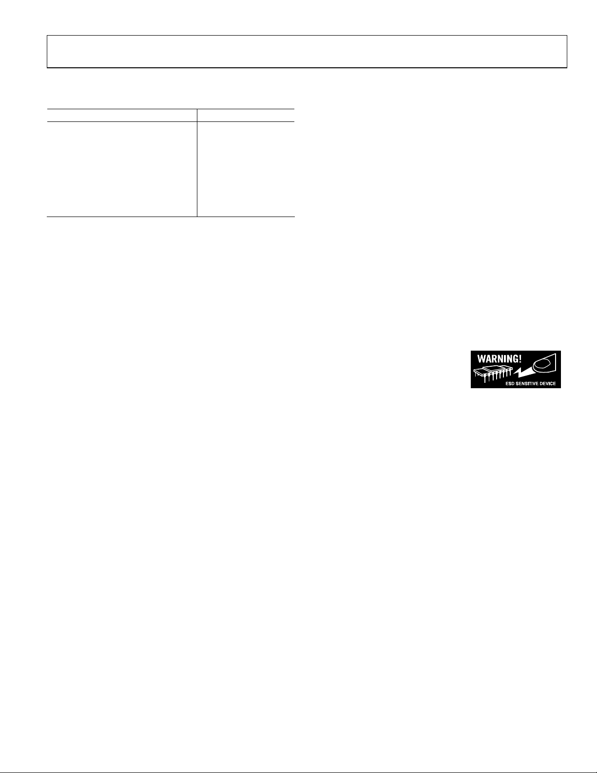
ABSOLUTE MAXIMUM RATINGS
Table 2.
Parameter Rating
Power Supply (V
Digital Output Current 5 mA
Digital Inputs −0.3 V to V
Analog Inputs −0.3 V to V
Operating Temperature −40°C to +85°C
Maximum Junction Temperature 150°C
Storage Temperature −65°C to +150°C
Lead Temperature (Soldering, 10 sec) 300°C
AVDD,VDVDD,VDRVDD
) 3.9 V
DRVDD
AVDD
+ 0.3 V
+ 0.3 V
Stresses above those listed under Absolute Maximum Ratings
may cause permanent damage to the device. This is a stress
rating only and functional operation of the device at these or
any other conditions above those indicated in the operational
section of this specification is not implied. Exposure to absolute
maximum rating conditions for extended periods may affect
device reliability.
EXPLANATION OF TEST LEVELS
I Devices are 100% production tested at +25°C and
guaranteed by design and characterization testing for
commercial operating temperature range (−40ºC to
+85°C).
II Parameter is guaranteed by design and/or
characterization testing.
III Parameter is a typical value only.
N/A Test level definition is not applicable.
THERMAL CHARACTERISTICS
Thermal Resistance
100-Lead MQFP
= 40.5°C/W
θ
JA
ESD CAUTION
ESD (electrostatic discharge) sensitive device. Electrostatic charges as high as 4000 V readily accumulate on the
human body and test equipment and can discharge without detection. Although this product features
proprietary ESD protection circuitry, permanent damage may occur on devices subjected to high energy
electrostatic discharges. Therefore, proper ESD precautions are recommended to avoid performance
degradation or loss of functionality.
Rev. A | Page 7 of 32
AD9879
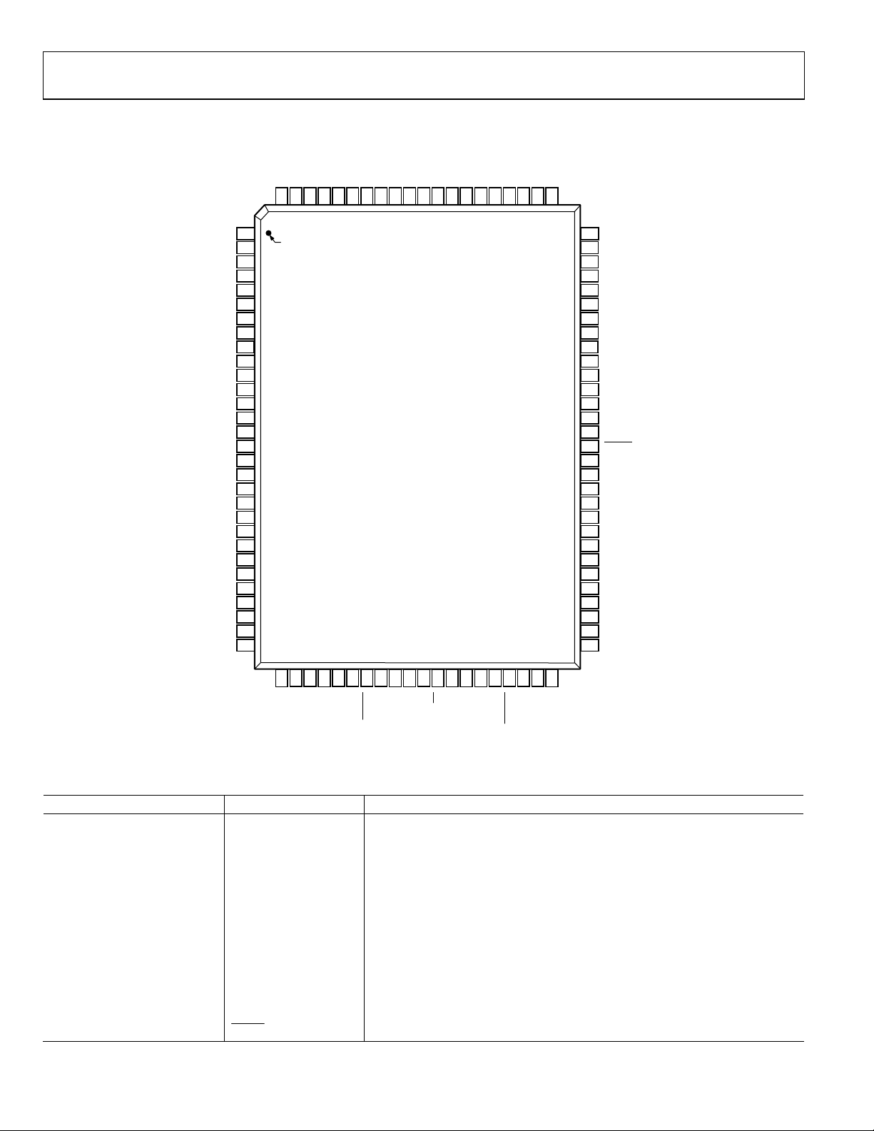
PIN CONFIGURATION AND FUNCTION DESCRIPTIONS
DNC
DRGND
DRVDD
IF(11)
IF(10)
IF(9)
IF(8)
IF(7)
IF(6)
IF(5)
IF(4)
IF(3)
IF(2)
IF(1)
IF(0)
RXIQ(3)
RXIQ(2)
RXIQ(1)
RXIQ(0)
RXSYNC
DRGND
DRVDD
MCLK
DVDD
DGND
TXSYNC
TXIQ(5)
TXIQ(4)
TXIQ(3)
TXIQ(2)
AGND
99
IF12+
98
IF12–
97
AGND
AVDD
969594
REFT12
REFB12
93
AVDD
AGND
IF10+
929190
AD9879
TOP VIEW
(Pins Down)
IF10–
AGND
898887
VIDEO IN
100
1
PIN 1
2
3
4
5
6
7
8
9
10
11
12
13
14
15
16
17
18
19
20
21
22
23
24
25
26
27
28
29
30
AVDD
REFB10
REFT10
868584
AGNDQ+Q–
AVDD
83
82
81
80
DNC
79
I+
78
I–
77
DNC
76
DNC
75
DNC
74
AGNDIQ
73
AVDDIQ
72
DRVDD
71
REFCLK
70
DRGND
69
DGND Σ-∆
68
Σ-∆_OUT
67
FLAG1
66
DVDD Σ-∆
65
CA_EN
64
CA_DATA
63
CA_CLK
62
DVDDOSC
61
OSCIN
60
XTAL
59
DGNDOSC
58
AGNDPLL
57
PLLFILT
56
AVDDPLL
55
DVDDPLL
54
DGNDPLL
53
AVDDTX
52
TX+
51
TX–
31
32TXIQ(0)
TXIQ(1)
33
DVDD
34
DGND
35
DNC
36
PROFILE
37
RESET
38
DVDD
39
DGND40DGND
SCLK
44
42
CS
SDO
SDIO
45
46
DVDDTX
DGNDTX
47
PWRDN
48
REFIO
49
FSADJ
50
AGNDTX
41
43
Figure 2. Pin Configuration
Table 3. Pin Function Descriptions
Pin No. Mnemonic Description
1, 35, 75 to 77, 80 DNC Do Not Connect. Pins are not bonded to die.
2, 21, 70 DRGND Pin Driver Digital Ground.
3, 22, 72 DRVDD Pin Driver Digital 3.3 V Supply.
4 to 15 IF[11:0] 12-Bit ADC Digital Output.
16 to 19 RXIQ[3:0] Muxed I and Q ADCs Output.
20 RXSYNC Sync Output, IF, I and Q ADCs.
23 MCLK Master Clock Output.
24, 33, 38 DVDD Digital 3.3 V Supply.
25, 34, 39, 40 DGND Digital Ground.
26 TXSYNC Sync Input for Transmit Port.
27 to 32 TXIQ[5:0] Digital Input for Transmit Port.
36 PROFILE Profile Selection Inputs.
37
RESET
Chip Reset Input (Active Low).
Rev. A | Page 8 of 32
02773-002
AD9879
Pin No. Mnemonic Description
41 SCLK SPORT Clock.
42
43 SDIO SPORT Data I/O.
44 SDO SPORT Data Output.
45 DGNDTX Tx Path Digital Ground.
46 DVDDTX Tx Path Digital 3.3 V Supply.
47
48 REFIO TxDAC Decoupling (to AGND).
49 FSADJ DAC Output Adjust (External Resistor).
50 AGNDTX Tx Path Analog Ground.
51, 52 TX−, TX+ Tx Path Complementary Outputs.
53 AVDDTX Tx Path Analog 3.3 V Supply.
54 DGNDPLL PLL Digital Ground.
55 DVDDPLL PLL Digital 3.3 V Supply.
56 AVDDPLL PLL Analog 3.3 V Supply.
57 PLLFILT PLL Loop Filter Connection.
58 AGNDPLL PLL Analog Ground.
59 DGNDOSC Oscillator Digital Ground.
60 XTAL Crystal Oscillator Inverted Output.
61 OSCIN Oscillator Clock Input.
62 DVDDOSC Oscillator Digital 3.3 V Supply.
63 CA_CLK Serial Clock to Cable Driver.
64 CA_DATA Serial Data to Cable Driver.
65
66 DVDD Σ-∆ Σ-∆ Digital 3.3 V Supply.
67 FLAG1 Digital Output Flag 1.
68 Σ-∆_OUT Σ-∆ DAC Output.
69 DGND Σ-∆ Σ-∆ Digital Ground.
71 REFCLK Programmable Reference Clock Output.
73 AVDDIQ 7-Bit ADCs Analog 3.3 V Supply.
74 AGNDIQ 7-Bit ADCs Analog Ground.
78, 79 I−, I+ Differential Input to I ADC.
81, 82 Q−, Q+ Differential Input to Q ADC.
83, 88, 91, 96, 99 AGND 12-Bit ADC Analog Ground.
84, 87, 92, 95 AVDD 12-Bit ADC Analog 3.3 V Supply.
85 REFB10 10-Bit ADC Decoupling Node.
86 REFT10 10-Bit ADC Decoupling Node.
89, 90 IF10−, IF10+ Differential Input to 10-Bit ADC.
93 REFB12 12-Bit ADC Decoupling Node.
94 REFT12 12-Bit ADC Decoupling Node.
97, 98 IF12−, IF12+ Differential Input to IF ADC.
100 VIDEO IN Video Clamp Input, 12-Bit ADC.
CS
PWRDN
CA_EN
SPORT Chip Select.
Power-Down Transmit Path.
Serial Enable to Cable Drive.
Rev. A | Page 9 of 32

AD9879
TERMINOLOGY
Aperture Delay
The aperture delay is a measure of the sample-and-hold
amplifier (SHA) performance. It specifies the time delay
between the rising edge of the sampling clock input and when
the input signal is held for conversion.
Aperture Uncertainty (Jitter)
Aperture jitter is the variation in aperture delay for successive
samples. It is manifested as noise on the input to the ADC.
Channel-to-Channel Isolation (Crosstalk)
In an ideal multichannel system, the signal in one channel does
not influence the signal level of another channel. The channelto-channel isolation specification is a measure of the change
that occurs to a grounded channel as a full-scale signal is
applied to another channel.
Differential Nonlinearity Error (DNL, No Missing Codes)
An ideal converter exhibits code transitions that are exactly 1 LSB
apart. DNL is the deviation from this ideal value. Guaranteed
no missing codes to 10-bit resolution indicates that all 1,024
codes, respectively, must be present over all operating ranges.
Effective Number of Bits (ENOB)
For a sine wave, SINAD can be expressed in terms of the
number of bits. Using the formula
N = (SINAD − 1.76 dB∕6.02)
it is possible to determine a measure of performance expressed
as N, the effective number of bits. Thus, the effective number of
bits for a device’s sine wave inputs at a given input frequency
can be calculated directly from its measured SINAD.
Gain Error
The first code transition should occur at an analog value
1/2 LSB above full scale. The last transition should occur for an
analog value 1 1/2 LSB below the nominal full scale. Gain error
is the deviation of the actual difference between the first and
last code transitions and the ideal difference between the first
and last code transitions.
Input Referred Noise
The rms output noise is measured using histogram techniques.
The standard deviation of the ADC output code is calculated in
LSB and converted to an equivalent voltage. This results in a
noise figure that can be directly referred to the input of the MxFE.
Integral Nonlinearity Error (INL)
Linearity error refers to the deviation of each individual code
from a line drawn from negative full scale through the positive
full scale. The point used as the negative full scale occurs
1/2 LSB before the first code transition. Positive full scale is
defined as a level 1 1/2 LSB beyond the last code transition. The
deviation is measured from the middle of each code to the true
straight line.
Offset Error
First transition should occur for an analog value 1/2 LSB
above −FS. Offset error is defined as the deviation of the actual
transition from that point.
Output Compliance Range
The range of allowable voltage at the output of a current-output
DAC. Operation beyond the maximum compliance limits can
cause either output stage saturation or break down, resulting in
nonlinear performance.
Phase Noise
Single-sideband phase noise power is specified relative to the
carrier (dBc/Hz) at a given frequency offset (1 kHz) from the
carrier. Phase noise can be measured directly in single-tone
transmit mode with a spectrum analyzer that supports noise
marker measurements. It detects the relative power between the
carrier and the offset (1 kHz) sideband noise and takes the
resolution bandwidth (RBW) into account by subtracting
10 log(RBW). It also adds a correction factor that compensates
for the implementation of the resolution bandwidth, log display,
and detector characteristic.
Pipeline Delay (Latency)
Pipeline delay is the number of clock cycles between conversion
initiation and the availability of the associated output data.
Power Supply Rejection
Power supply rejection specifies the converter’s maximum fullscale change when the supplies are varied from nominal to
minimum and maximum specified voltages.
Signal-to-Noise and Distortion (SINAD) Ratio
SINAD is the ratio of the rms value of the measured input
signal to the rms sum of all other spectral components below
the Nyquist frequency, including harmonics but excluding dc.
The value for SINAD is expressed in decibels.
Signal-to-Noise Ratio (SNR)
SNR is the ratio of the rms value of the measured input signal to
the rms sum of all other spectral components below the Nyquist
frequency, excluding harmonics and dc. The value for SNR is
expressed in decibels.
Spurious-Free Dynamic Range (SFDR)
SFDR is the difference, in dB, between the rms amplitude of the
DAC output signal (or the ADC input signal) and the peak
spurious signal over the specified bandwidth (Nyquist
bandwidth, unless otherwise noted).
Total Harmonic Distortion (THD)
THD is the ratio of the rms sum of the first six harmonic
components to the rms value of the measured input signal, and
is expressed as a percentage or in decibels.
Rev. A | Page 10 of 32
 Loading...