ANALOG DEVICES AD9878 Service Manual
Mixed-Signal Front End
FEATURES
Low cost 3.3 V CMOS MxFE™ for broadband applications
DOCSIS, EURO-DOCSIS, DVB, DAVIC compliant
232 MHz quadrature digital upconverter
12-bit direct IF DAC (TxDAC+®)
Up to 65 MHz carrier frequency DDS
Programmable sampling clock rates
Analog Tx output level adjust
Dual 12-bit, 29 MSPS direct IF ADCs with video clamp input
10-bit, 29 MSPS sampling ADC
8-bit ∑-∆ auxiliary DAC
Direct interface to AD832x family of PGA cable drivers
APPLICATIONS
Cable set-top boxes
Cable and wireless modems
GENERAL DESCRIPTION
The AD9878 is a single-supply, cable modem/set-top box,
mixed-signal front end. The device contains a transmit path
interpolation filter, a complete quadrature digital upconverter,
and a transmit DAC. The receive path contains dual 12-bit
ADCs and a 10-bit ADC. All internally required clocks and an
output system clock are generated by the phase-locked loop
(PLL) from a single crystal oscillator or clock input.
The transmit path interpolation filter provides an upsampling
factor of 16× with an output signal bandwidth up to 4.35 MHz.
Carrier frequencies up to 65 MHz with 26 bits of frequency tuning
resolution can be generated by the direct digital synthesizer
(DDS). The transmit DAC resolution is 12 bits and can run at
sampling rates as high as 232 MSPS. Analog output scaling from
0 dB to 7.5 dB in 0.5 dB steps is available to preserve SNR when
reduced output levels are required.
for Broadband Applications
AD9878
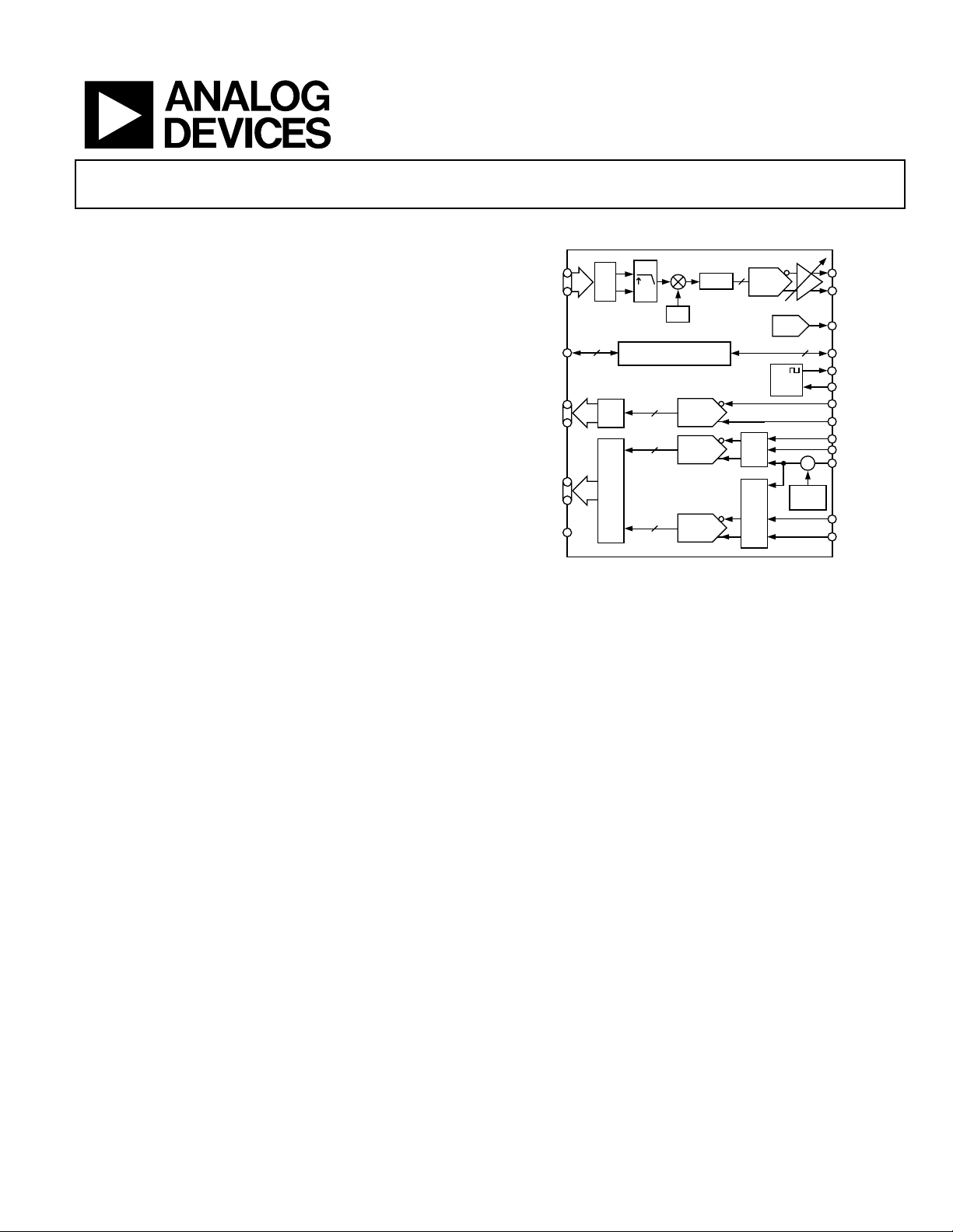
FUNCTIONAL BLOCK DIAGRAM
I
16
TxID[5:0]
SDIO
IF10[4:0]
IF12[11:0]
FLAG[2:1]
Tx
Q
4
CONTROL REGISTERS
MUX
MUX
DDS
10
ADC
12
ADC
12
ADC
Figure 1.
The 12-bit ADCs provide excellent undersampling performance,
allowing this device to typically deliver better than 10 ENOBs
with IF inputs up to 70 MHz. The 12-bit IF ADCs can sample at
rates up to 29 MHz, allowing them to process wideband signals.
The AD9878 includes a programmable ∑-∆ DAC, which can be
used to control an external component such as a variable gain
amplifier (VGA) or a voltage controlled tuner.
The AD9878 also integrates a CA port that enables a host
processor to interface with the AD832x family of programmable
gain amplifier (PGA) cable drivers or industry equivalent via
the MxFE serial port (SPORT).
The AD9878 is available in a 100-lead, LQFP package. The
AD9878 is specified over the extended industrial (−40°C to
+85°C) temperature range.
SINC
12
–1
DAC
Σ-∆
PLL
MUX
CLAMP
MUX
3
Σ
LEVEL
Tx
Σ-∆ OUTPUT
CA PORT
MCLK
OSCIN
IF10 INPUT
IF12B INPUT
VIDEO IN
–
IF12A INPUT
03277-001
Rev. A
Information furnished by Analog Devices is believed to be accurate and reliable.
However, no responsibility is assumed by Analog Devices for its use, nor for any
infringements of patents or other rights of third parties that may result from its use.
Specifications subject to change without notice. No license is granted by implication
or otherwise under any patent or patent rights of Analog Devices. Trademarks and
registered trademarks are the property of their respective owners.
One Technology Way, P.O. Box 9106, Norwood, MA 02062-9106, U.S.A.
Tel: 781.329.4700 www.analog.com
Fax: 781.326.8703 © 2005 Analog Devices, Inc. All rights reserved.

AD9878
TABLE OF CONTENTS
Electrical Characteristics ................................................................. 4
Transmit Timing......................................................................... 21
Absolute Maximum Ratings............................................................ 7
Explanation of Test Levels........................................................... 7
Thermal Characteristics .............................................................. 7
ESD Caution.................................................................................. 7
Pin Configuration and Function Descriptions............................. 8
Typical Performance Characteristics ........................................... 10
Terminology .................................................................................... 13
Register Bit Definitions.................................................................. 14
Register 0x00—Initialization .................................................... 15
Register 0x01—Clock Configuration....................................... 15
Register 0x02—Power-Down.................................................... 15
Register 0x03—Flag Control..................................................... 15
Register 0x04—∑-∆ Control Word........................................... 15
Register 0x07—Video Input Configuration............................ 16
Register 0x08—ADC Clock Configuration ............................ 16
Register 0x0C—Die Revision.................................................... 16
Register 0x0D—Tx Frequency Tuning Words LSBs.............. 16
Register 0x0E—DAC Gain Control ......................................... 16
Register 0x0F—Tx Path Configuration................................... 16
Registers 0x10 Through 0x17—Burst Parameter ................... 17
Serial Interface for Register Control............................................ 18
General Operation of the Serial Interface............................... 18
Instruction Byte .......................................................................... 18
Serial Interface Port Pin Descriptions..................................... 18
MSB/LSB Transfers..................................................................... 19
Notes on Serial Port Operation ................................................19
Theory of Operation ...................................................................... 20
Transmit Path.............................................................................. 21
Interpolation Filter..................................................................... 21
Half-Band Filters (HBFs).......................................................... 21
Cascade Integrator Comb (CIC) Filter.................................... 21
Combined Filter Response........................................................ 21
Digital Upconverter ................................................................... 22
Tx Signal Level Considerations................................................ 22
Tx Throughput and Latency..................................................... 23
DAC.............................................................................................. 23
Programming the AD8321/AD8323 or
AD8322/AD8327/AD8238 Cable-Driver Amplifiers............ 23
OSCIN Clock Multiplier ........................................................... 24
Clock and Oscillator Circuitry ................................................. 24
Programmable Clock Output REFCLK .................................. 24
Power-Up Sequence ................................................................... 26
Reset ............................................................................................. 26
Transmit Power-Down .............................................................. 26
∑-∆ Outputs ................................................................................ 27
Receive Path (Rx) ....................................................................... 27
IF10 and IF12 ADC Operation ................................................ 27
ADC Voltage References ........................................................... 29
Video Input ................................................................................. 29
PCB Design Considerations.......................................................... 30
Component Placement .............................................................. 30
Power Planes and Decoupling.................................................. 30
Ground Planes............................................................................ 30
Signal Routing............................................................................. 30
Outline Dimensions....................................................................... 36
Ordering Guide .......................................................................... 36
Data Assembler........................................................................... 21
Rev. A | Page 2 of 36

AD9878
REVISION HISTORY
3/05—Rev. 0 to Rev. A
Changed OSCOUT to REFCLK.................................................. Universal
Changes to Electrical Characteristics ........................................................4
Changes to Pin Configuration and Function Descriptions....................8
Changes to ∑-∆ Output Signals (Figure 32)............................................27
Change to ∑-∆ RC Filter (Figure 33) .......................................................27
Changes to Evaluation PCB Schematic (Figure 38 and Figure 39)......31
Updated Outline Dimensions...................................................................36
Changes to Ordering Guide......................................................................36
5/03—Revision 0: Initial Version
Rev. A | Page 3 of 36

AD9878
ELECTRICAL CHARACTERISTICS
VAS = 3.3 V ± 5%, VDS = 3.3 V ± 10%, f
= 4.02 kΩ, maximum. Fine gain, 75 Ω DAC load.
R
SET
Table 1.
PARAMETER Temp Test Level Min Typ Max Unit
OSCIN and XTAL CHARACTERISTICS
Frequency Range Full II 3 29 MHz
Duty Cycle 25°C II 35 50 65 %
Input Impedance 25°C III 100||3 MΩ||pF
MCLK Cycle-to-Cycle Jitter (f
derived from PLL) 25°C III 6 ps rms
MCLK
Tx DAC CHARACTERISTICS
Maximum Sample Rate Full II 232 MHz
Resolution N/A N/A 12 Bits
Full-Scale Output Current Full II 4 10 20 mA
Gain Error (Using Internal Reference) 25°C I −2.0 −1 +2.0 % FS
Offset Error 25°C I ±1.0 % FS
Reference Voltage (REFIO Level) 25°C I 1.18 1.23 1.28 V
Differential Nonlinearity (DNL) 25°C III ±2.5 LSB
Integral Nonlinearity (INL) 25°C III ±8 LSB
Output Capacitance 25°C III 5 pF
Phase Noise @ 1 kHz Offset, 42 MHz Carrier 25°C III −110 dBc/Hz
Output Voltage Compliance Range Full II −0.5 +1.5 V
Wideband SFDR
5 MHz Analog Output, I
65 MHz Analog Output, I
= 10 mA Full II 62.4 68 dB
OUT
= 10 mA Full II 50.3 53.5 dB
OUT
Narrow-Band SFDR (±1 MHz Window)
5 MHz Analog Output, I
65 MHz Analog Output, I
= 10 mA Full II 71 74 dB
OUT
= 10 mA Full II 61 64 dB
OUT
Tx MODULATOR CHARACTERISTICS
I/Q Offset Full II 50 55 dB
Pass-Band Amplitude Ripple (f < f
Pass-Band Amplitude Ripple (f < f
Stop-Band Response (f > f
× 3/4) Full II −63 dB
IQCLK
Tx GAIN CONTROL
Gain Step Size 25°C III 0.5 dB
Gain Step Error 25°C III <0.05 dB
Settling Time, 1% (Full-Scale Step) 25°C III 1.8 µs
10-BIT ADC CHARACTERISTICS
Resolution N/A N/A 10 Bits
Maximum Conversion Rate Full II 29 MHz
Pipeline Delay N/A N/A 4.5 ADC cycles
Analog Input
Input Voltage Range Full II 2 V
Differential Input Impedance 25°C III 4||2 kΩ||pF
Full Power Bandwidth 25°C III 90 MHz
Dynamic Performance (AIN = −0.5 dBFS, f = 5 MHz)
Signal-to-Noise and Distortion (SINAD) Full II 57.6 59.7 dB
Effective Number of Bits (ENOB) Full II 9.3 9.6 Bits
Total Harmonic Distortion (THD) Full II −71.1 −63.6 dB
Spurious-Free Dynamic Range (SFDR) Full II 65.7 72.4 dB
Reference Voltage Error, REFT10 to REFB10 (1.0 V) Full I ±4 ±100 mV
= 27 MHz, f
OSCIN
/8) Full II ±0.1 dB
IQCLK
/4) Full II ±0.5 dB
IQCLK
= 216 MHz, f
SYSCLK
= 54 MHz (M = 8), ADC clock derived from OSCIN,
MCLK
PPD
Rev. A | Page 4 of 36
AD9878
PARAMETER Temp Test Level Min Typ Max Unit
Dynamic Performance (AIN = −0.5 dBFS, f = 50 MHz)
Signal-to-Noise and Distortion (SINAD) Full II 54.8 57.8 dB
Effective Number of Bits (ENOB) Full II 8.8 9.3 Bits
Total Harmonic Distortion (THD) Full II −63.3 −56.9 dB
Spurious-Free Dynamic Range (SFDR) Full II 56.9 63.7 dB
12-BIT ADC CHARACTERISTICS
Resolution N/A N/A 12 Bits
Maximum Conversion Rate Full II 29 MHz
Pipeline Delay N/A N/A 5.5 ADC cycles
Analog Input
Input Voltage Range Full III 2 V
Differential Input Impedance 25°C III 4||2 kΩ||pF
Aperture Delay 25°C III 2.0 ns
Aperture Jitter 25°C III 1.2 ps rms
Full Power Bandwidth 25°C III 85 MHz
Input Referred Noise 25°C III 75 µV
Reference Voltage Error, REFT12 to REFB12 (1 V) Full I −100 ±16 +100 mV
Dynamic Performance (AIN = −0.5 dBFS, f = 5 MHz)
ADC Sample Clock = OSCIN
Signal-to-Noise and Distortion (SINAD) Full II 61.0 67 dB
Effective Number of Bits (ENOBs) Full II 9.8 10.8 Bits
Signal-to-Noise Ratio (SNR) Full II 64.2 66 dB
Total Harmonic Distortion (THD) Full II −72.7 −61.7 dB
Spurious-Free Dynamic Range (SFDR) Full II 62.8 74.6 dB
ADC Sample Clock = PLL
Signal-to-Noise and Distortion (SINAD) Full II 60.4 64.4 dB
Effective Number of Bits (ENOB) Full II 9.74 10.4 Bits
Signal-to-Noise Ratio (SNR) Full II 62.4 65.1 dB
Total Harmonic Distortion (THD) Full II −72.7 −61.8 dB
Spurious-Free Dynamic Range (SFDR) Full II 62.7 74.6 dB
Dynamic Performance (AIN = −0.5 dBFS, f = 50 MHz)
ADC Sample Clock = OSCIN
Signal-to-Noise and Distortion (SINAD) Full II 61.0 65.2 dB
Effective Number of Bits (ENOB) Full II 9.8 10.5 Bits
Signal-to-Noise Ratio (SNR) Full II 64.2 67.4 dB
Total Harmonic Distortion (THD) Full II −72.8 −61.8 dB
Spurious-Free Dynamic Range (SFDR) Full II 62.8 74.6 dB
Differential Phase 25°C III <0.1 Degrees
Differential Gain 25°C III <1 LSB
VIDEO ADC PERFORMANCE (AIN = −0.5 dBFS, f = 5 MHz)
ADC Sample Clock = OSCIN
Signal-to-Noise and Distortion (SINAD) Full II 46.7 53 dB
Signal-to-Noise Ratio (SNR) Full II 54.3 63.2 Bits
Total Harmonic Distortion (THD) Full II −50.2 −45.9 dB
Spurious-Free Dynamic Range (SFDR) Full II 45.9 50 dB
CHANNEL-TO-CHANNEL ISOLATION
Tx DAC-to-ADC Isolation (5 MHz Analog Output)
Isolation Between Tx and 10-Bit ADC 25°C III >60 dB
Isolation Between Tx and 12-Bit ADCs 25°C III >80 dB
ADC-to-ADC Isolation (AIN = –0.5 dBFS, f = 5 MHz)
Isolation Between IF10 and IF12A/B 25°C III >85 dB
Isolation Between IF12A and IF12B 25°C III >85 dB
PPD
Rev. A | Page 5 of 36

AD9878
PARAMETER Temp Test Level Min Typ Max Unit
TIMING CHARACTERISTICS (10 pF Load)
Wake-Up Time N/A N/A 200 t
Minimum RESET Pulse Width Low, tRL
N/A N/A 5 t
Digital Output Rise/Fall Time Full II 2.8 4 ns
Tx/Rx Interface
MCLK Frequency, f
Full II 58 MHz
MCLK
TxSYNC/TxIQ Setup Time, tSU Full II 3 ns
TxSYNC/TxIQ Hold Time, tHU Full II 3 ns
MCLK Rising Edge to RxSYNC Valid Delay, tMD Full II 0 1.0 ns
REFCLK Rising or Falling Edge to
RxSYNC Valid Delay, t
OD
Full II
/
t
OSCIN
4 − 2.0
t
OSCIN
/
4 + 3.0
REFCLK Edge to MCLK Falling Edge, tEE Full II −1.0 +1.0 ns
SERIAL CONTROL BUS
Maximum SCLK Frequency, f
Minimum Clock Pulse Width High, t
Minimum Clock Pulse Width Low, t
Full II 15 MHz
SCLK
Full II 30 ns
PWH
Full II 30 ns
PWL
Maximum Clock Rise/Fall Time Full II 1 µs
Minimum Data/Chip-Select Setup Time, tDS Full II 25 ns
Minimum Data Hold Time, tDH Full II 0 ns
Maximum Data Valid Time, tDV Full II 30 ns
CMOS LOGIC INPUTS
Logic 1 Voltage 25°C II V
− 0.7 V
DRVDD
Logic 0 Voltage 25°C II 0.4 V
Logic 1 Current 25°C II 12 µA
Logic 0 Current 25°C II 12 µA
Input Capacitance 25°C III 3 pF
CMOS LOGIC OUTPUTS (1 mA Load)
Logic 1 Voltage 25°C II V
− 0.6 V
DRVDD
Logic 0 Voltage 25°C II 0.4 V
POWER SUPPLY
Supply Current, IS (Full Operation) 25°C II 184 204 mA
Analog Supply Current, IAS 25°C III 105 115 mA
Digital Supply Current, IDS 25°C III 79 89 mA
Supply Current, IS
Standby (PWRDN Pin Active, IAS + IDS )
25°C II 124 137 mA
Full Power-Down (Register 0x02 = 0xFF) 25°C II 46 52 mA
Power-Down Tx Path (Register 0x02 = 0x60) 25°C III 124 mA
Power-Down IF12 Rx Path (Register 0x02 = 0x1B) 25°C III 131 159 mA
Power Supply Rejection (Differential Signal)
Tx DAC 25°C III <0.25 % FS
10-Bit ADC 25°C III <0.0001 % FS
12-Bit ADC 25°C III <0.0004 % FS
ns
MCLK
MCLK
cycles
cycles
Rev. A | Page 6 of 36
AD9878
ABSOLUTE MAXIMUM RATINGS
Table 2.
Parameter Rating
Power Supply (V
Digital Output Current 5 mA
Digital Inputs −0.3 V to V
Analog Inputs −0.3 V to V
Operating Temperature −40°C to +85°C
Maximum Junction Temperature 150°C
Storage Temperature −65°C to +150°C
Lead Temperature (Soldering, 10 sec) 300°C
AVDD
, V
DVDD
, V
) 3.9 V
DRVDD
DRVDD
AVDD
+ 0.3 V
+ 0.3 V
Stresses above those listed under Absolute Maximum Ratings
may cause permanent damage to the device. This is a stress
rating only; functional operation of the device at these or any
other condition s above those indicated in the operational
section of this specification is not implied. Exposure to absolute
maximum rating conditions for extended periods may affect
device reliability.
EXPLANATION OF TEST LEVELS
I. Devices are 100% production tested at 25°C and guaranteed
II. Parameter is guaranteed by design and/or characterization
III. Parameter is a typical value only.
N/A. Test level definition is not applicable.
THERMAL CHARACTERISTICS
Thermal resistance of 100-lead LQFP: θJA = 40.5°C/W
by design and characterization testing for extended industrial
operating temperature range (−40°C to +85°C).
testing.
ESD CAUTION
ESD (electrostatic discharge) sensitive device. Electrostatic charges as high as 4000 V readily accumulate on
the human body and test equipment and can discharge without detection. Although this product features
proprietary ESD protection circuitry, permanent damage may occur on devices subjected to high energy
electrostatic discharges. Therefore, proper ESD precautions are recommended to avoid performance
degradation or loss of functionality.
Rev. A | Page 7 of 36
AD9878
PIN CONFIGURATION AND FUNCTION DESCRIPTIONS
AVDD
AGND
VIDEO IN
AGND
IF12A+
IF12A–
AGND
AVDD
REFT12A
REFB12AAVDD
AGND
IF12B+
IF12B–
AGND
AVDD
39
40
41CS42
SCLK
DVDD
DGND
DRGND
DRVDD
(MSB) IF12(11)
IF12(10)
IF12(9)
IF12(8)
IF12(7)
IF12(6)
IF12(5)
IF12(4)
IF12(3)
IF12(2)
IF12(1)
IF12(0)
(MSB) IF10(4)
IF10(3)
IF10(2)
IF10(1)
IF10(0)
RxSYNC
DRGND
DRVDD
MCLK
DVDD
DGND
100
99 98 97 96 95 94 93 92 91 90 89 88 87 86 85 84 83 82 81 80 79 78 77
1
2
3
4
5
6
7
8
9
10
11
12
13
14
15
16
17
18
19
20
21
22
23
24
25
26
27
TxSYNC
(MSB) TxIQ(5)
TxIQ(4)28TxIQ(3)29TxIQ(2)30TxIQ(1)31TxIQ(0)
32
33
34
DVDD
35
DGND
AD9878
TOP VIEW
(Not to Scale)
36
37
DVDD
DGND
38
RESET
PROFILE
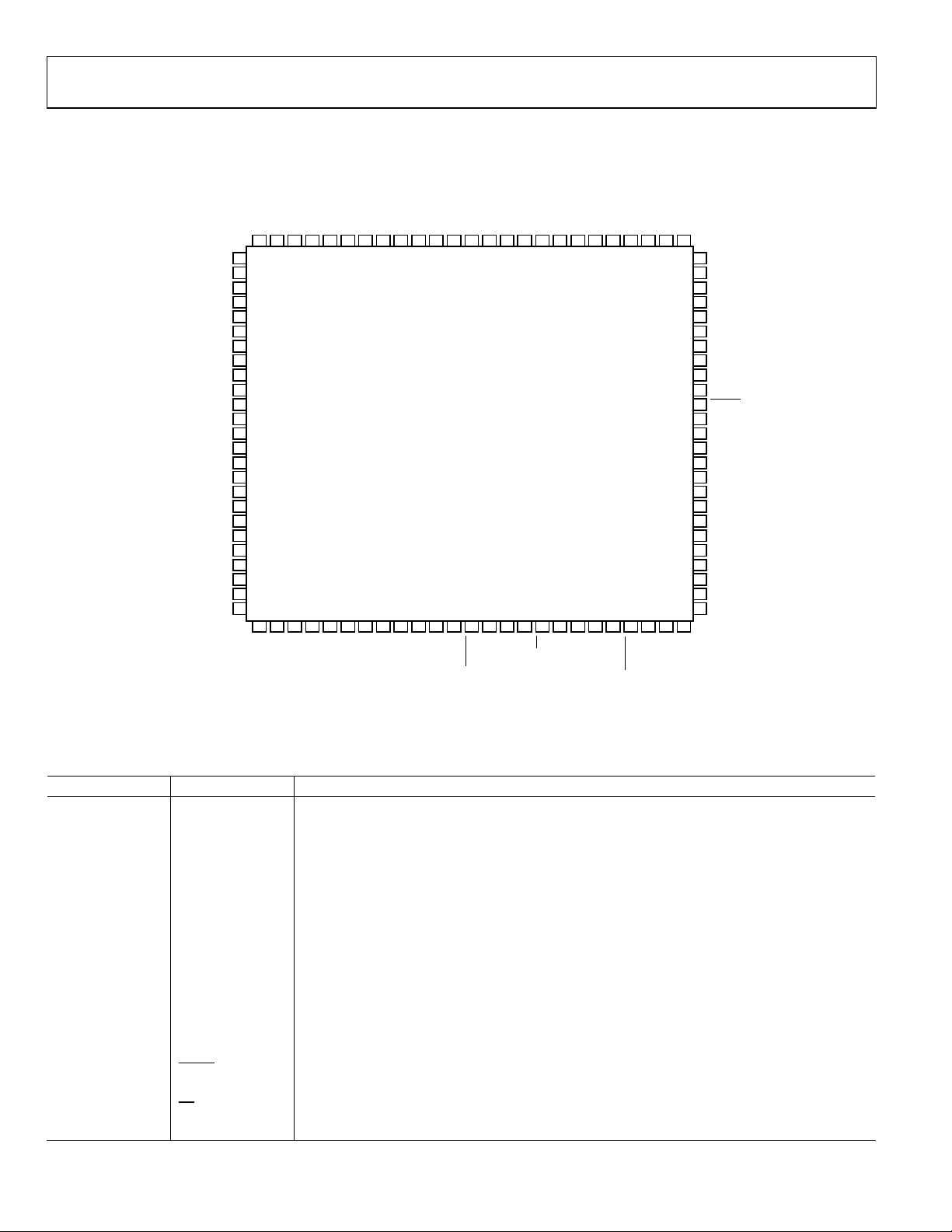
Figure 2. Pin Configuration
REFT12B
43
REFB12BAVDD
44
SDIO
SDO
AGND
45
46
DGNDTx
AVDD10
47
DVDDTx
AGND10
PWRDN
48
IF10+
49
REFIO
IF10–
FSADJ
AGND
76
75
74
73
72
71
70
69
68
67
66
65
64
63
62
61
60
59
58
57
56
55
54
53
52
51
50
AGNDTx
REFT10
REFB10
AGND10
AVDD10
DRVDD
DRGND
REFCLK
SIGDELT
FLAG1
FLAG2
CA_EN
CA_DATA
CA_CLK
DVDDOSC
OSCIN
XTAL
DGNDOSC
AGNDPLL
PLLFILT
AVDDPLL
DVDDPLL
DGNDPLL
AVDDTx
Tx+
Tx–
03277-002
Table 3. Pin Function Descriptions
Pin No. Mnemonic Descriptions
1, 21, 70 DRGND Pin Driver Digital Ground
2, 22, 71 DRVDD Pin Driver Digital 3.3 V Supply
3 (MSB) IF12(11) 12-Bit ADC Digital Ouput
4 to 14 IF12[10:0] 12-Bit ADC Digital Ouput
15 (MSB) IF10(4) 10-Bit ADC Digital Ouput
16 to 19 IF10[3:0] 10-Bit ADC Digital Ouput
20 RxSYNC Sync Output, 10-Bit and 12-Bit ADCs
23 MCLK Master Clock Output
24, 33, 35, 39 DVDD Digital 3.3 V Supply
25, 34, 36, 40 DGND Digital Ground
26 TxSYNC Sync Input for Transmit Port
27 (MSB) TxIQ(5) Digital Input for Transmit Port
28 to 32 TxIQ[4:0] Digital Input for Transmit Port
37 PROFILE Profile Selection Input
38
RESET
Chip Reset Input
41 SCLK SPORT Clock
42
CS
SPORT Chip Select
43 SDIO SPORT Data I/O
Rev. A | Page 8 of 36
AD9878
Pin No. Mnemonic Descriptions
44 SDO SPORT Data Output
45 DGNDTx Tx Path Digital Ground
46 DVDDTx Tx Path Digital 3.3 V Supply
47
48 REFIO TxDAC Decoupling (to AGND)
49 FSADJ DAC Output Adjust (External Resistor)
50 AGNDTx Tx Path Analog Ground
51, 52 Tx−, Tx+ Tx Path Complementary Outputs
53 AVDDTx Tx Path Analog 3.3 V Supply
54 DGNDPLL PLL Digital Ground
55 DVDDPLL PLL Digital 3.3 V Supply
56 AVDDPLL PLL Analog 3.3 V Supply
57 PLLFILT PLL Loop Filter Connection
58 AGNDPLL PLL Analog Ground
59 DGNDOSC Oscillator Digital Ground
60 XTAL Crystal Oscillator Inverted Output
61 OSCIN Oscillator Clock Input
62 DVDDOSC Oscillator Digital 3.3 V Supply
63 CA_CLK Serial Clock-to-Cable Driver
64 CA_DATA Serial Data-to-Cable Driver
65
66, 67 FLAG[2:1] Programmable Flag Outputs
68 SIGDELT ∑-∆ DAC Output
69 REFCLK Reference Clock Output
72, 80 AVDD10 10-Bit ADC Analog 3.3 V Supply
73, 79 AGND10 10-Bit ADC Analog Ground
74 REFB10 10-Bit ADC Reference Decoupling Node
75 REFT10 10-Bit ADC Reference Decoupling Node
76, 81, 86, 89, 94,
97, 99
77, 78 IF10−, IF10+ Differential Input to 10-bit ADC
82, 85, 90, 93, 100 AVDD 12-Bit ADC Analog 3.3 V Supply
83 REFB12B ADC12B Reference Decoupling Node
84 REFT12B ADC12B Reference Decoupling Node
87, 88 IF12B−, IF12B+ Differential Input to ADC12B
91 REFB12A ADC12A Reference Decoupling Node
92 REFT12A ADC12A Reference Decoupling Node
95, 96 IF12A−, IF12A+ Differential Input to ADC12A
98 VIDEO IN Video Clamp Input
PWRDN
CA_EN
AGND 12-Bit ADC Analog Ground
Power-Down Transmit Path
Serial Enable-to-Cable Driver
Rev. A | Page 9 of 36
AD9878
TYPICAL PERFORMANCE CHARACTERISTICS
0
–10
–20
–30
–40
–50
–60
MAGNITUDE (dB)
–70
–80
–90
–100
024681012141618
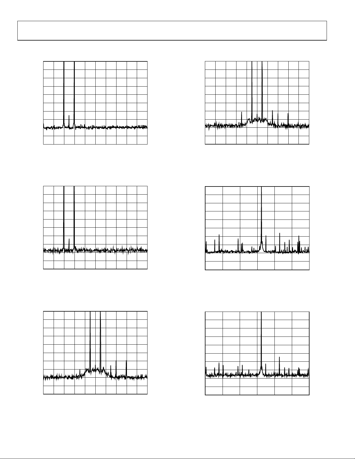
Figure 3. Dual-Sideband Spectral Plot, f
R
SET
= 10 kΩ (I
FREQUENCY (MHz)
= 4 mA), RBW = 1 kHz
OUT
C
= 5 MHz, f = 1 MHz,
03277-022
20
0
–10
–20
–30
–40
–50
–60
MAGNITUDE (dB)
–70
–80
–90
–100
55 57 59 61 63 65 67 69 71 73
Figure 6. Dual-Sideband Spectral Plot, f
R
SET
= 4 kΩ (I
FREQUENCY (MHz)
= 65 MHz, f = 1 MHz,
= 10 mA), RBW = 1 kHz
OUT
C
03277-025
75
0
–10
–20
–30
–40
–50
–60
MAGNITUDE (dB)
–70
–80
–90
–100
024681012141618
Figure 4. Dual-Sideband Spectral Plot, f
R
SET
0
–10
–20
–30
–40
–50
–60
MAGNITUDE (dB)
–70
–80
–90
–100
55 57 59 61 63 65 67 69 70 73
Figure 5. Dual-Sideband Spectral Plot, f
f = 1 MHz, R
= 4 kΩ (I
= 10 kΩ (I
SET
FREQUENCY (MHz)
= 5 MHz, f = 1 MHz,
= 10 mA), RBW = 1 kHz
OUT
FREQUENCY (MHz)
OUT
C
= 4 mA), RBW = 1 kHz
= 65 MHz,
C
20
75
03277-023
03277-024
0
–10
–20
–30
–40
–50
–60
MAGNITUDE (dB)
–70
–80
–90
–100
0 20406080100
Figure 7. Single Sideband @ 65 MHz, f
f = 1 MHz, R
0
–10
–20
–30
–40
–50
–60
MAGNITUDE (dB)
–70
–80
–90
–100
0 20406080100
Figure 8. Single Sideband @ 65 MHz, f
f = 1 MHz, R
FREQUENCY (MHz)
= 10 kΩ (I
SET
FREQUENCY (MHz)
= 4 kΩ (I
SET
= 66 MHz,
= 4 mA), RBW = 2 kHz
OUT
= 10 mA), RBW = 2 kHz
OUT
C
= 66 MHz,
C
120
120
03277-026
03277-027
Rev. A | Page 10 of 36
AD9878
0
–10
–20
–30
–40
–50
–60
MAGNITUDE (dB)
–70
–80
–90
–100
0 20406080100
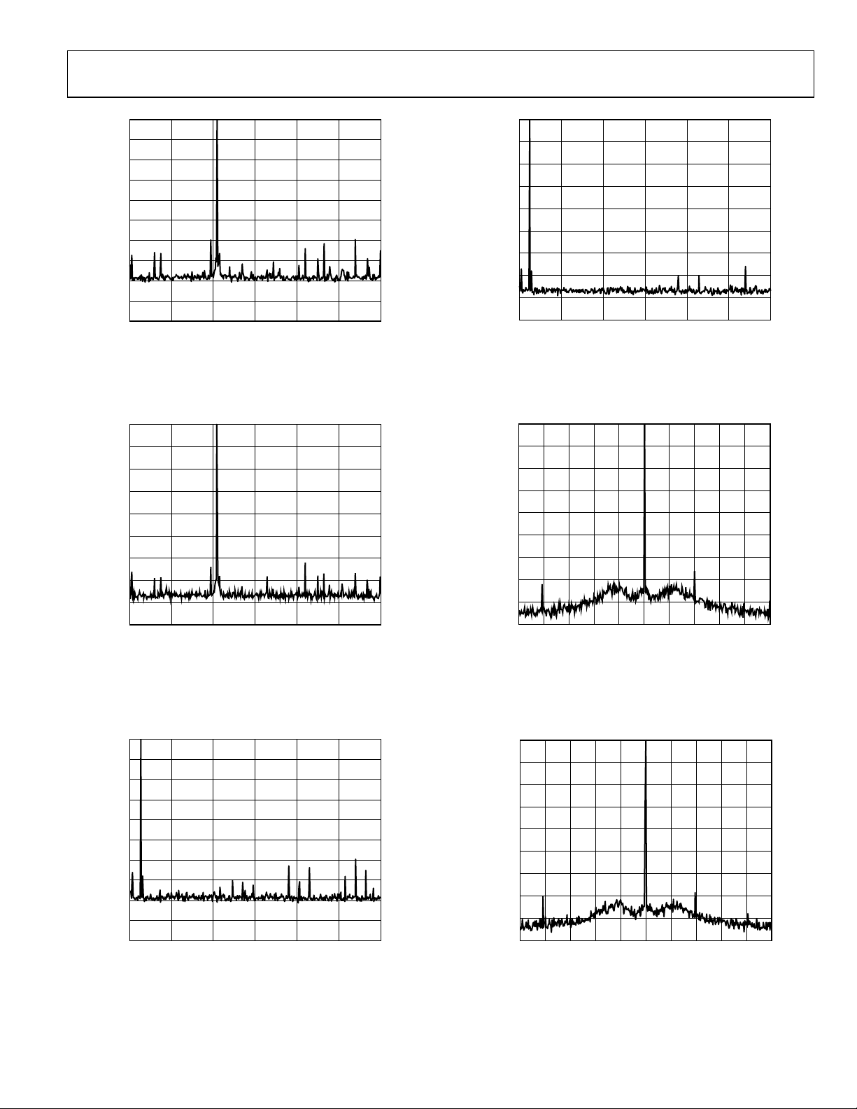
Figure 9. Single Sideband @ 42 MHz, f
f = 1 MHz, R
FREQUENCY (MHz)
= 10 kΩ (I
SET
= 43 MHz,
= 4 mA), RBW = 2 kHz
OUT
C
03277-028
120
0
–10
–20
–30
–40
–50
–60
MAGNITUDE (dB)
–70
–80
–90
0 20406080100
Figure 12. Single Sideband @ 5 MHz, f
f = 1 MHz, R
FREQUENCY (MHz)
= 4 kΩ (I
SET
= 6 MHz,
= 10 mA), RBW = 2 kHz
OUT
C
03277-031
120
0
–10
–20
–30
–40
–50
–60
MAGNITUDE (dB)
–70
–80
–90
0 20406080100
Figure 10. Single Sideband @ 42 MHz, f
f = 1 MHz, R
0
–10
–20
–30
–40
–50
–60
MAGNITUDE (dB)
–70
–80
–90
–100
0 20406080100
Figure 11. Single Sideband @ 5 MHz, f
f = 1 MHz, R
FREQUENCY (MHz)
= 4 kΩ (I
SET
FREQUENCY (MHz)
= 10 kΩ (I
SET
= 43 MHz,
= 10 mA), RBW = 2 kHz
OUT
= 4 mA), RBW = 2 kHz
OUT
C
= 6 MHz,
C
120
120
03277-029
03277-030
0
–10
–20
–30
–40
–50
–60
MAGNITUDE (dB)
–70
–80
–90
–2.5 –2.0 –1.5 –1.0 –0.5 0 0.5 1.0 1.5 2.0
Figure 13. Single Sideband @ 65 MHz, f
f = 1 MHz, R
0
–10
–20
–30
–40
–50
–60
MAGNITUDE (dB)
–70
–80
–90
–2.5 –2.0 –1.5 –1.0 –0.5 0 0.5 1.0 1.5 2.0
Figure 14. Single Sideband @ 65 MHz, f
f = 1 MHz, R
FREQUENCY (MHz)
= 10 kΩ (I
SET
FREQUENCY (MHz)
= 4 kΩ (I
SET
= 66 MHz,
= 4 mA), RBW = 500 Hz
OUT
= 10 mA), RBW = 500 Hz
OUT
C
= 66 MHz,
C
03277-032
2.5
03277-033
2.5
Rev. A | Page 11 of 36
 Loading...