a
A
Broadband Modem
Mixed-Signal Front End
AD9875
FEATURES
Low Cost 3.3 V-CMOS Mixed-Signal Front End (
Converter for Broadband Modems
10-/12-Bit D/A Converter (TxDAC+
®
)
MxFE™
)
64/32 MSPS Input Word Rate
2/4 Interpolating LPF or BPF Transmit Filter
128 MSPS DAC Output Update Rate
Wide (26 MHz) Transmit Bandwidth
Power-Down Mode
10-/12-Bit, 50 MSPS A/D Converter
Fourth Order Low-Pass Filter 12 MHz or 26 MHz
with Bypass
–6 dB to +36 dB Programmable Gain Amplifier
Internal Clock Multiplier (PLL)
Clock Outputs
Voltage Regulator Controller
48-Lead LQFP Package
APPLICATIONS
Powerline Networking
Home Phone Networking
xDSL
Broadband Wireless
Home RF
PRODUCT DESCRIPTION
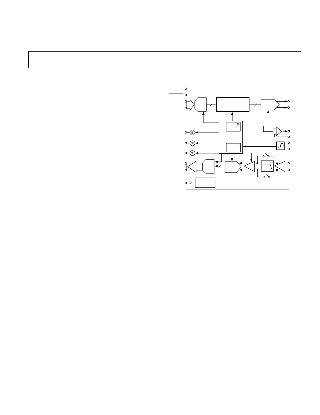
The AD9875 is a single-supply broadband modem mixedsignal front end (MxFE) IC. The devices contain a transmit
path Interpolation Filter and DAC, and a receive path PGA,
LPF, and ADC supporting a variety of broadband modem
applications. Also on chip is a PLL clock multiplier that provides all required clocks from a single crystal or clock input.
The AD9875 provides 10-bit converter performance on both
the Tx and Rx paths.
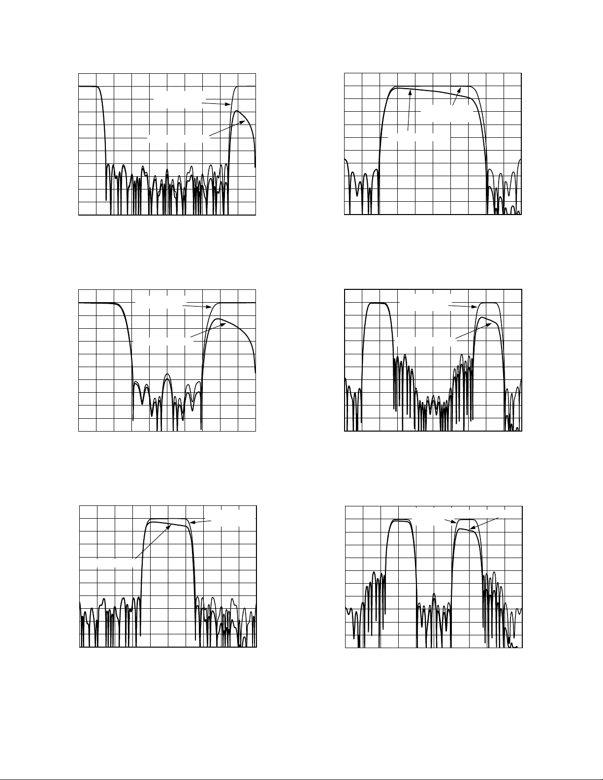
The TxDAC+ uses a selectable digital 2× or 4× interpolation
low-pass or band-pass filter to further oversample transmit
data and reduce the complexity of analog reconstruction filtering.
The transmit path signal bandwidth can be as high as 26 MHz
at an input data rate of 64 MSPS. The 10-bit DAC provides
differential current outputs for optimum noise and distortion
performance. The DAC full-scale current can be adjusted
from 2 mA to 20 mA by a single resistor, providing 20 dB of
additional gain range.
The receive path consists of a PGA, LPF, and ADC. The two-stage
PGA has a gain range of –6 dB to +36 dB, and is programmable
in 2 dB steps, adding 42 dB of dynamic range to the receive path.
FUNCTIONAL BLOCK DIAGRAM
PWR DN
Tx QUIET
GAIN
Tx [5:0]
Tx SYNC
CLK-A
CLK-B
Rx SYNC
Rx [5:0]
SPORT
3
10 10
Tx
MUX
REGISTER
CONTROL
Rx
MUX
10
Kx INTERPOLATION
LPF/BPF
PLL-A
CLOCK GEN
PLL-B
M/N
ADC
L
PGA
AD9875
TxDAC+
V
REF
VRC
LPF
PGA
Tx+
Tx–
GATE
FB
OSCIN
XTAL
Rx+
Rx–
The receive path LPF cutoff frequency can be programmed to either
12 MHz or 26 MHz. The filter cutoff frequency can also be tuned
or bypassed where filter requirements differ. The 10-bit ADC
uses a multistage differential pipeline architecture to achieve
excellent dynamic performance with low power consumption.
The AD9875 provides a voltage regulator controller (VRC) that
can be used with an external power MOSFET transistor to form
a cost-effective 1.3 V linear regulator.
The digital transmit and receive ports are each multiplexed to a
bus width of 5/6 bits and are clocked at a frequency of twice the
10-bit word rate.
The AD9875 ADC and/or DAC can also be used at higher
sampling rates as high as 64 MSPS in a 5-bit resolution nonmultiplexed mode.
The AD9875 is pin compatible with the 12-bit AD9876. Both are
available in a space-saving 48-lead LQFP package. They are specified
over the industrial (–40°C to +85°C) temperature range.
MxFE is a trademark of Analog Devices, Inc.
TxDAC+ is a registered trademark of Analog Devices, Inc.
REV. A
Information furnished by Analog Devices is believed to be accurate and
reliable. However, no responsibility is assumed by Analog Devices for its
use, nor for any infringements of patents or other rights of third parties that
may result from its use. No license is granted by implication or otherwise
under any patent or patent rights of Analog Devices.
One Technology Way, P.O. Box 9106, Norwood, MA 02062-9106, U.S.A.
Tel: 781/329-4700 www.analog.com
Fax: 781/326-8703 © Analog Devices, Inc., 2002

AD9875–SPECIFICATIONS
(VS = 3.3 V 10%, f
100 DAC single-ended load, unless otherwise noted.)
= 32 MHz, f
OSCIN
= 128 MHz, Gain = –6 dB, R
DAC
= 4.02 k,
SET
Test
Parameter Temp Level Min Typ Max Unit
OSC IN CHARACTERISTICS
Frequency Range Full II 10 64 MHz
Duty Cycle 25°CII 40 5060 %
Input Capacitance 25°C III 3 pF
Input Impedance 25°C III 100 MΩ
CLOCK OUTPUT CHARACTERISTICS
CLKA Jitter (f
Derived from PLL) 25°C III 14 ps rms
CLKA
CLKA Duty Cycle 25°C III 50 ±5%
CLKB Jitter (f
Derived from PLL) 25°C III 33 ps rms
CLKB
CLKB Duty Cycle 25°C III 50 ± 5%
Tx CHARACTERISTICS
Tx Path Latency, 4× Interpolation Full II 82 f
DAC
Cycles
Interpolation Filter Bandwidth (–0.1 dB)
4× Interpolation, LPF Full II 13 MHz
2× Interpolation, LPF Full II 26 MHz
TxDAC
Resolution Full II 10 Bits
Conversion Rate Full II 10 128 MHz
Full-Scale Output Current Full II 2 10 20 mA
Voltage Compliance Range Full II –0.5 +1.5 V
Gain Error Full II –5 ± 2+5 % FS
Output Offset Full II 0 7 19 µA
Differential Nonlinearity 25°C III 0.5 LSB
Integral Nonlinearity 25°C III 1 LSB
Output Capacitance 25°C III 5 pF
Phase Noise @ 1 kHz Offset, 10 MHz Signal 25°C III –90 dBc/Hz
Signal-to-Noise and Distortion (SINAD)
10 MHz Analog Out AD9875 (20 MHz BW) Full I 59 61 dB
Wideband SFDR (to Nyquist, 64 MHz Max) 25°C III
5 MHz Analog Out 25°C III 78 dBc
10 MHz Analog Out 25°C III 72 dBc
Narrowband SFDR (3 MHz Window)
10 MHz Analog Out 25°C III 80 dBc
IMD (f1 = 6.9 MHz, f2 = 7.1 MHz) 25°C III –76 dBFS
Rx PATH CHARACTERISTICS
Resolution Full II 10 Bits
Conversion Rate Full II 7.5 55 MHz
Pipeline Delay, ADC Clock Cycles Full II 5.5 Cycles
DC Accuracy
Differential Nonlinearity 25°CII –1.0 ± 0.25 +1.0 LSB
Integral Nonlinearity 25°CII –2.0 ± 0.5 +2.0 LSB
Dynamic Performance
= –0.5 dBFS, f = 5 MHz)
(A
IN
OSCIN
= 32 MHz
@ f
Signal-to-Noise and Distortion Ratio (SINAD) 25°C III 59.6 dB
Effective Number of Bits (ENOB) 25°C III 9.5 Bits
Signal-to-Noise Ratio (SNR) 25°C III 60 dB
Total Harmonic Distortion (THD) 25°C III –65 dB
Spurious Free Dynamic Range (SFDR) 25°C III 68 dB
Dynamic Performance
AIN = –0.5 dBFS, f = 10 MHz
(
PLLB/2
= 50 MHz
@ F
)
Signal-to-Noise and Distortion Ratio (SINAD) 25°C III 54 dB
Effective Number of Bits (ENOB) 25°C III 8.6 Bits
Signal-to-Noise Ratio (SNR) 25°C III 55 dB
Total Harmonic Distortion (THD) 25°C III –61 dB
Spurious Free Dynamic Range (SFDR) 25°C III 68 dB
–2–
REV. A

AD9875
Test
Parameter Temp Level Min Typ Max Unit
Rx PATH GAIN/OFFSET
Minimum Programmable Gain 25°C III –6 dB
Maximum Programmable Gain
(12 MHz Filter) 25°C III 36 dB
(26 MHz Filter) 25°C III 30 dB
Gain Step Size 25°C III 2 dB
Gain Step Accuracy 25°C III ± 0.4 dB
Gain Range Error 25°C III ± 1.0 dB
Offset Error, PGA Gain = 0 dB (AD9875) 25°C III ± 4.0 LSB
Absolute Gain Error, PGA Gain = 0 dB 25°C III ±0.8 dB
Rx PATH INPUT CHARACTERISTICS
Input Voltage Range 25°C III 4 Vppd
Input Capacitance 25°C III 4 pF
Differential Input Resistance 25°C III 270 Ω
Input Bandwidth (–3 dB) 25°C III 50 MHz
Input Referred Noise (at +36 dB Gain with Filter) 25°C III 16 µV rms
Input Referred Noise (at –6 dB Gain with Filter) 25°C III 684 µV rms
Common-Mode Rejection 25°C III 40 dB
Rx PATH LPF (Low Cutoff Frequency)
Cutoff Frequency 25°C III 12 MHz
Cutoff Frequency Variation 25°C III ± 7%
Attenuation @ 22 MHz 25°C III 20 dB
Passband Ripple 25°C III ± 1.0 dB
Group Delay Variation 25°C III 30 ns
Settling Time
(to 1% FS, Min to Max Gain Change) 25°C III 150 ns
Total Harmonic Distortion at Max Gain (THD) 25°C III –68 dBc
Rx PATH LPF (High Cutoff Frequency)
Cutoff Frequency 25°C III 26 MHz
Cutoff Frequency Variation 25°C III ± 7%
Attenuation @ 44 MHz 25°C III 20 dB
Passband Ripple 25°C III ± 1.2 dB
Group Delay Variation 25°C III 15 ns
Settling Time
(to 1% FS, Min to Max Gain Change) 25°C III 80 ns
Total Harmonic Distortion at Max Gain (THD) 25°C III –65 dBc
Rx PATH DIGITAL HPF
Latency (ADC Clock Source Cycles) Full II 1 Cycle
Roll-Off in Stopband Full II 6 dB/Octave
–3 dB Frequency Full II f
Rx PATH DISTORTION PERFORMANCE
IMD: f1 = 6.9 MHz, f2 = 7.1 MHz
12 MHz Filter: 0 dB 25°C III –65 dBc
: 30 dB 25°C III –57 dBc
28 MHz Filter: 0 dB 25°C III –65 dBc
: 30 dB 25°C III –56 dBc
POWER-DOWN/DISABLE TIMING
Power-Up Delay (Power-Down-to-Active)
DAC 25°CII 40 µs
PLL 25°CII 10 µs
ADC 25°CII 1000 µs
PGA 25°CII 1 µs
LPF 25°CII 1 µs
Interpolator 25°CII 200 ns
VRC 25°CII 2 µs
Minimum RESET Pulsewidth Low (t
DAC I
DAC I
Off after Tx QUIET Asserted 25°CII 200 ns
OUT
On after Tx QUIET Deasserted 25°CII 1 µs
OUT
) Full III 5 f
RL
Power-Down Delay (Active-to-Power-Down)
DAC 25°CII 400 ns
Interpolator 25°CII 200 ns
/400 Hz
ADC
OSCIN
Cycle
REV. A
–3–

AD9875
–SPECIFICATIONS (continued)
Test
Parameter Temp Level Min Typ Max Unit
Tx PATH INTERFACE
Maximum Input Nibble Rate, 2× Interpolation Full II 128 MHz
Tx-Set Up Time (t
) Full II 3.0 ns
SU
Tx-Hold Time (tHD) Full II 0 ns
Rx PATH INTERFACE
Maximum Output Nibble Rate Full I 110 MHz
Rx-DataValid Time (t
) Full II 3.0 ns
VT
Rx-Data Hold Time (tHT) Full II 1.5 ns
CMOS LOGIC INPUTS
Logic “1” Voltage Full II
V
– 0.7 V
DRVDD
Logic “0” Voltage Full II 0.4 V
Logic “1” Current Full II 12 µA
Logic “0” Current Full II 12 µA
Input Capacitance 25°C III 3 µF
CMOS LOGIC OUTPUTS (1 mA Load)
Logic “1” Voltage Full II
V
– 0.6 V
DRVDD
Logic “0” Voltage Full II 0.4 V
Digital Output Rise/Fall Time Full II 1.5 2.5 ns
POWER SUPPLY
All Blocks Powered Up
I
I
Digital Supply Current (I
Analog Supply Current (I
(Total Supply Current) Full I 262 288 mA
S_TOTAL
(Tx_QUIET Pin Asserted) 25°C III 172 mA
S_TOTAL
+ I
DRVDD
)25°C III 185 mA
AVDD
)25°C III 77 mA
DVDD
Power Consumption of Functional Blocks
Rx LPF 25°C III 110 mA
ADC and FPGA 25°C III 55 mA
Rx Reference 25°C III 2 mA
Interpolator 25°C III 33 mA
DAC 25°C III 18 mA
PLL-B 25°C III 8 mA
PLL-A 25°C III 24 mA
Voltage Regulator Controller 25°C III 1 mA
All Blocks Powered Down
Supply Current I
Supply Current I
S
S
, f
= 32 MHz Full II 19 22 mA
OSCIN
, f
Idle Full II 10 12 mA
OSCIN
Power Supply Rejection
Tx Path (∆V
= ⫾10%) 25°C III 62 dB
S
Rx Path (∆VS = ⫾10%) 25°C III 54 dB
SERIAL CONTROL BUS
Maximum SCLK Frequency (f
Clock Pulsewidth High (t
Clock Pulsewidth Low (t
PWH
PWL
) Full II 25 MHz
SCLK
) Full II 18 ns
) Full II 18 ns
Clock Rise/Fall Time Full II 1 ms
Data/Chip-Select Setup Time (t
Data Hold Time (t
) Full II 0 ns
DH
) Full II 25 ns
DS
Data Valid Time (tDV) Full II 20 ns
RECEIVE-TO-TRANSMIT ISOLATION
(10 MHz, Full-Scale Sinewave Output/Output)
Isolation: Tx Path to Rx Path, Gain = +36 dB 25°C III –75 dB
Isolation: Rx Path to Tx Path, Gain = –6 dB 25°C III –70 dB
VOLTAGE REGULATOR CONTROLLER
Output Voltage (V
Line Regulation (∆V
Load Regulation (∆V
Maximum Load Current (I
Specifications subject to change without notice.
with SI2301 Connected) Full I 1.25 1.30 1.35 V
FB
FB%
FB
/∆V
/∆I
LOAD
× 100%) 25°C III 100 %
DVDD%
)25°C III 60 mΩ
) Full II 250 mA
LOAD
–4–
REV. A
AD9875
ABSOLUTE MAXIMUM RATINGS*
Power Supply (VS) . . . . . . . . . . . . . . . . . . . . . . . . . . . . . 3.9 V
Digital Output Current . . . . . . . . . . . . . . . . . . . . . . . . . 5 mA
Digital Inputs . . . . . . . . . . . . . . . . . –0.3 V to DRVDD 0.3 V
Analog Inputs . . . . . . . . . . . . . . . . . . –0.3 V to AVDD 0.3 V
Operating Temperature . . . . . . . . . . . . . . . . . –40°C to +85°C
Maximum Junction Temperature . . . . . . . . . . . . . . . . 150°C
EXPLANATION OF TEST LEVELS
I–Devices are 100% production tested at 25°C and guaranteed
by design and characterization testing for industrial operating
temperature range (–40°C to +85°C).
II – Parameter is guaranteed by design and/or characterization
testing.
III –Parameter is a typical value only.
Storage Temperature . . . . . . . . . . . . . . . . . . –65°C to +150°C
Lead Temperature (Soldering 10 sec) . . . . . . . . . . . . . 300°C
*Stresses greater than those listed under Absolute Maximum Ratings may cause
permanent damage to the device. This is a stress rating only; functional operation
of the device at these or any other conditions above those indicated in the
operational section of this specification is not implied. Exposure to absolute
maximum rating conditions for extended periods may affect device reliability.
ORDERING GUIDE
THERMAL CHARACTERISTICS
Thermal Resistance
48-Lead LQFP
JA = 57°C/W
= 28°C/W
JC
Model Temperature Range Package Description Package Option
AD9875BST –40°C to +85°C 48-Lead LQFP ST-48
AD9875-EB –40°C to +85°CEvaluation Board
AD9875BSTRL –40°C to +85°CBST Reel
CAUTION
ESD (electrostatic discharge) sensitive device. Electrostatic charges as high as 4000 V readily
accumulate on the human body and test equipment and can discharge without detection. Although
the AD9875 features proprietary ESD protection circuitry, permanent damage may occur on
devices subjected to high energy electrostatic discharges. Therefore, proper ESD precautions are
recommended to avoid performance degradation or loss of functionality.
WARNING!
ESD SENSITIVE DEVICE
REV. A
–5–
AD9875
PIN FUNCTION DESCRIPTIONS
Pin Name Function
1 OSCIN Crystal Oscillator Inverter Input
2 SENABLE Serial Bus Enable Input
3 SCLK Serial Bus Clock Input
4 SDATA Serial Bus Data I/O
5, 38, 47 AVDD Analog 3.3 V Power Supply
6, 9, 39, 42, 43, 46 AVSS Analog Ground
7Tx+ Transmit DAC+ Output
8 Tx– Transmit DAC– Output
10 FSADJ DAC Full-Scale Output Current Adjust with External Resistor
11 REFIO DAC Bandgap Decoupling Node
12 PWR DN Power-Down Input
13 DVSS Digital Ground
14 DVDD Digital 3.3 V Power Supply
15 FB Regulator Feedback Input
16 GATE Regulator Output to FET Gate
17 GAIN Transmit Data Port (Tx[5:0]) Mode Select Input
18 Tx QUIET Transmit Quiet Input
19–24 Tx[5:0] Transmit Data Input
25 Tx SYNC Transmit Synchronization Strobe Input
26 CLK-A L × f
27 CLK-B M/N × f
28 Rx SYNC Receive Data Synchronization Strobe Output
29–34 Rx[5:0] Receive Data Output
35 DRVDD Digital I/O 3.3 V Power Supply
36 DRVSS Digital I/O Ground
37 RESET Reset Input
40 REFB ADC Reference Decoupling Node
41 REFT ADC Reference Decoupling Node
44 Rx+ Receive Path + Input
45 Rx– Receive Path – Input
48 XTAL Crystal Oscillator Inverter Output
Clock Output
OSCIN
OSCIN
Clock Output
OSCIN
SENABLE
SCLK
SDATA
AVDD
AVSS
Tx+
Tx–
AVSS
FSADJ
REFIO
PWR DN
PIN CONFIGURATION
XTAL
AVDD
AVSS
Rx–
Rx+
AVSS
AVSS
AD9875
GAIN
Tx QUIET
Tx [5]
REFT
Tx [4]
48 4 7 46 4 5 44 39 38 3743 42 41 40
1
PIN 1
2
IDENTIFIER
3
4
5
6
7
8
9
10
11
12
13 14 15 16 17 18 19 20 21 22 23 24
DVSS
FB
DVDD
TOP VIEW
(Not to Scale)
GATE
–6–
REFB
Tx [3]
AVSS
Tx [2]
AVDD
Tx [1]
RESET
36
35
34
33
32
31
30
29
28
27
26
25
Tx [0]
DRVSS
DRVDD
Rx [0]
Rx [1]
Rx [2]
Rx [3]
Rx [4]
Rx [5]
Rx SYNC
CLK-B
CLK-A
Tx SYNC
REV. A

AD9875
DEFINITIONS OF SPECIFICATIONS
CLOCK JITTER
The clock jitter is a measure of the intrinsic jitter of the PLL
generated clocks. It is a measure of the jitter from one rising
and of the clock with respect to another edge of the clock nine
cycles later.
DIFFERENTIAL NONLINEARITY ERROR (DNL, NO MISSING CODES)
An ideal converter exhibits code transitions that are exactly 1 LSB
apart. DNL is the deviation from this ideal value. Guaranteed
no missing codes to 10-bit resolution indicates that all 1024
codes respectively, must be present over all operating ranges.
INTEGRAL NONLINEARITY ERROR (INL)
Linearity error refers to the deviation of each individual code from
a line drawn from “negative full scale” through “positive full
scale.” The point used as “negative full scale” occurs 1/2 LSB
before the first code transition. “positive full scale” is defined as
a level 1 1/2 LSB beyond the last code transition. The deviation
is measured from the middle of each particular code to the true
straight line.
PHASE NOISE
Single-sideband phase noise power density is specified relative to
the carrier (dBc/Hz) at a given frequency offset (1 kHz) from the
carrier. Phase noise can be measured directly on a generated single
tone with a spectrum analyzer that supports noise marker measurements. It detects the relative power between the carrier and
the offset (1 kHz) sideband noise and takes the resolution bandwidth (rbw) into account by subtracting 10 log(rbw). It also adds
a correction factor that compensates for the implementation of the
resolution bandwidth, log display and detector characteristic.
OUTPUT COMPLIANCE RANGE
The range of allowable voltage at the output of a current-output
DAC. Operation beyond the maximum compliance limits may
cause either output stage saturation, resulting in nonlinear performance or breakdown.
SPURIOUS–FREE DYNAMIC RANGE (SFDR)
The difference, in dB, between the rms amplitude of the DACs
output signal (or ADC’s input signal) and the peak spurious
signal over the specified bandwidth (Nyquist bandwidth unless
otherwise noted).
PIPELINE DELAY (LATENCY)
The number of clock cycles between conversion initiation and
the associated output data being made available.
OFFSET ERROR
First transition should occur for an analog value 1/2 LSB above
negative full scale. Offset error is defined as the deviation of the
actual transition from that point.
GAIN ERROR
The first code transition should occur at an analog value 1/2 LSB
above negative full scale. The last transition should occur for an
analog value 1 1/2 LSB below the nominal full scale. Gain error
is the deviation of the actual difference between first and last
code transitions and the ideal difference between first and last
code transitions.
INPUT REFERRED NOISE
The rms output noise is measured using histogram techniques.
The ADC output codes’ standard deviation is calculated in LSB,
and converted to an equivalent voltage. This results in a noise
figure that can be directly referred to the Rx input of the AD9875.
SIGNAL-TO-NOISE AND DISTORTION RATIO (SINAD)
SINAD is the ratio of the rms value of the measured input signal to
the rms sum of all other spectral components below the Nyquist
frequency, including harmonics but excluding dc. The value for
SINAD is expressed in decibels.
EFFECTIVE NUMBER OF BITS (ENOB)
For a sine wave, SINAD can be expressed in terms of the number
of bits. Using the following formula,
N = (SINAD – 1.76) dB/6.02
it is possible to get a measure of performance expressed as N,
the effective number of bits.
SIGNAL-TO-NOISE RATIO (SNR)
SNR is the ratio of the rms value of the measured input signal to
the rms sum of all other spectral components below the Nyquist
frequency, excluding harmonics and dc. The value for SNR is
expressed in decibels.
TOTAL HARMONIC DISTORTION (THD)
THD is the ratio of the rms sum of the first six harmonic com-
ponents to the rms value of the measured input signal and is
expressed as a percentage or in decibels.
POWER SUPPLY REJECTION
Power Supply Rejection specifies the converters maximum
full-scale change when the supplies are varied from nominal to
minimum and maximum specified voltages.
REV. A
–7–
AD9875
–Typical Tx Digital Filter Performance Characteristics
10
0
–10
–20
–30
–40
–50
–60
MAGNITUDE – dB
–70
–80
–90
–100
0.0 0.1 0.2 0.3 0.4 0.5 0.6 0.7 0.8 0.9 1.0
INTERPOLATION
FILTER
INCLUDING SIN(X)/X
NORMALIZED – f
s
TPC 1. 4 Low-Pass Interpolation Filter
10
0
–10
–20
–30
–40
–50
–60
MAGNITUDE – dB
–70
–80
–90
–100
0.0 0.1 0.2 0.3 0.4 0.5 0.6 0.7 0.8 0.9 1.0
INTERPOLATION
FILTER
INCLUDING SIN(X)/X
NORMALIZED – f
S
TPC 2. 2 Low-Pass Interpolation Filter
10
0
–10
–20
–30
–40
–50
–60
MAGNITUDE – dB
–70
–80
–90
–100
0.0 0.1 0.2 0.3 0.4 0.5 0.6 0.7 0.8 0.9 1.0
INCLUDING SIN(X)/X
INTERPOLATION
FILTER
NORMALIZED – f
S
TPC 4. 2 Bandpass Interpolation Filter, fS /2 Modulation,
Adjacent Image Preserved
10
0
–10
–20
–30
–40
–50
–60
MAGNITUDE – dB
–70
–80
–90
–100
0.0 0.1 0.2 0.3 0.4 0.5 0.6 0.7 0.8 0.9 1.0
INTERPOLATION
FILTER
INCLUDING SIN(X)/X
NORMALIZED – fS
TPC 5. 4 Bandpass Interpolation Filter, fS /4 Modulation,
Lower Image Preserved
10
0
–10
–20
–30
INCLUDING SIN(X)/X
–40
–50
–60
MAGNITUDE – dB
–70
–80
–90
–100
0.0 0.1 0.2 0.3 0.4 0.5 0.6 0.7 0.8 0.9 1.0
NORMALIZED – f
INTERPOLATION
S
FILTER
TPC 3. 4 Bandpass Interpolation Filter, fS /2 Modulation,
Adjacent Image Preserved
10
0
–10
–20
–30
–40
–50
–60
MAGNITUDE – dB
–70
–80
–90
–100
0.0 0.1 0.2 0.3 0.4 0.5 0.6 0.7 0.8 0.9 1.0
INTERPOLATION
FILTER
NORMALIZED – fS
INCLUDING SIN(X)/X
TPC 6. 4 Bandpass Interpolation Filter, fS /4 Modulation,
Upper Image Preserved
–8–
REV. A
f
OUT
– MHz
90
85
60
80
75
70
65
132465798101211 13 1514 16 1817
MAGNITUDE – dBc
f
DATA
= 50MSPS
f
DATA
= 50MSPS
FREQUENCY – MHz
0
10
–10
–20
–30
–40
–50
–60
–70
–80
–90
–100
7.56.5 6.6 6.7 6.8 6.9 7.0 7.1 7.2 7.3 7.4
MAGNITUDE – dBc
FREQUENCY – MHz
0
10
–10
–20
–30
–40
–50
–60
–70
–80
–90
–100
7.56.5 6.6 6.7 6.8 6.9 7.0 7.1 7.2 7.3 7.4
MAGNITUDE – dBc
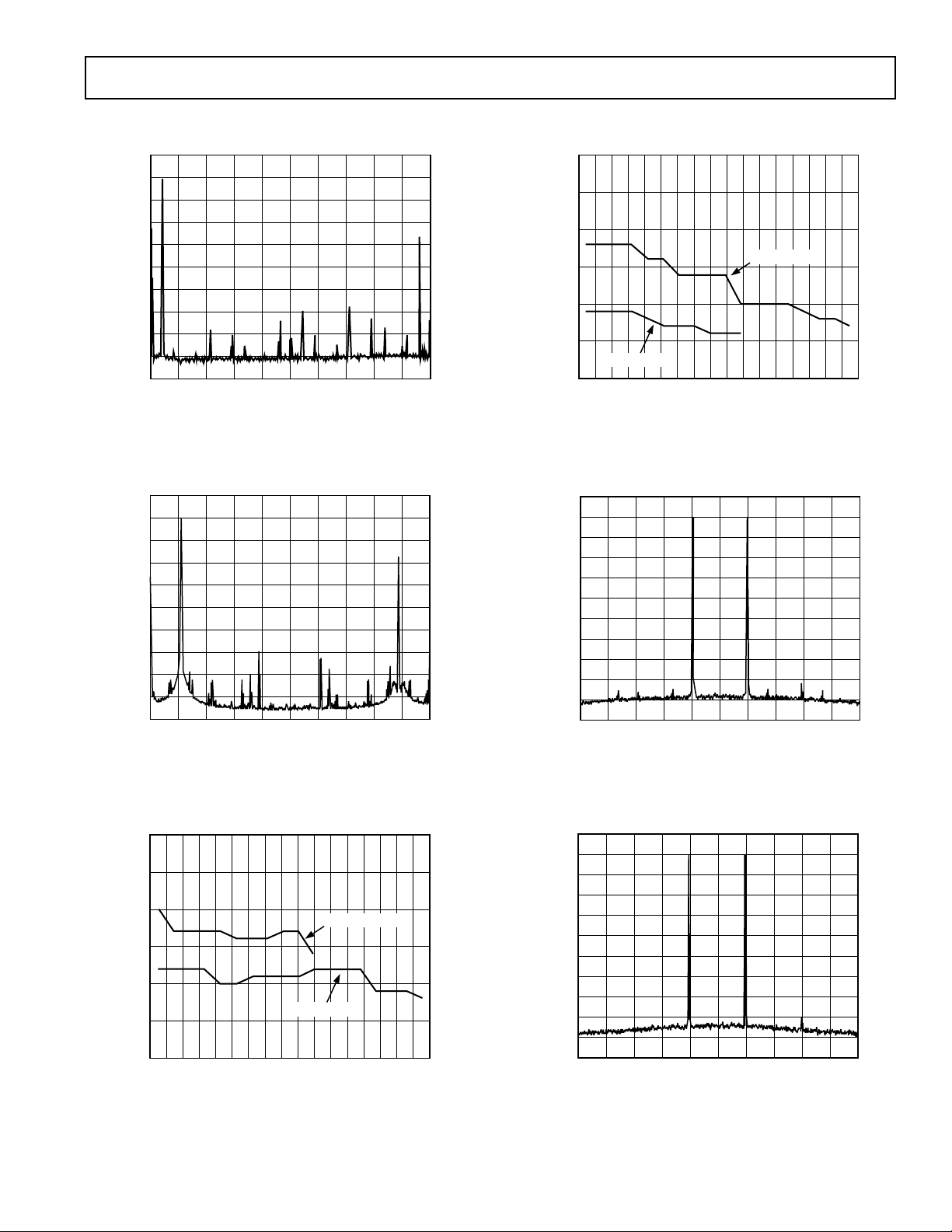
Typical AC Characteristics Curves for TxDAC
10
0
–10
–20
–30
–40
–50
MAGNITUDE – dBc
–60
–70
–80
–90
01326385164 7790102 115 128
FREQUENCY – MHz
(R
= 4.02 k, R
SET
= 100 )
DAC
AD9875
TPC 7. Single Tone Spectral Plot @ f
f
= 5 MHz, 4 LPF
OUT
10
0
–10
–20
–30
–40
–50
MAGNITUDE – dBc
–60
–70
–80
–90
010203040506070 8090100
FREQUENCY – MHz
TPC 8. Single Tone Spectral Plot @ f
= 11 MHz, 2 LPF
f
OUT
90
85
= 32 MSPS,
DATA
= 50 MSPS,
DATA
TPC 10. “Out of Band” SFDR vs. f
and 50 MSPS
TPC 11. Dual Tone Spectral Plot @ f
= 6.9 MHz and 7.1 MHz, 4 LPF
f
OUT
OUT
@ f
DATA
= 32 MSPS,
DATA
= 32 MSPS
80
75
REV. A
70
MAGNITUDE – dBc
65
60
132465798101211 13 1514 16 1817
TPC 9. “In Band” SFDR vs. f
and 50 MSPS
f
OUT
f
DATA
– MHz
OUT
f
DATA
= 50MSPS
@ f
DATA
= 32MSPS
= 32 MSPS
TPC 12. Dual Tone Spectral Plot @ f
= 6.9 MHz and 7.1 MHz, 2 LPF
f
OUT
–9–
= 50 MSPS,
DATA
 Loading...