IF Digitizing Subsystem
FEATURES
10 MHz to 300 MHz Input Frequency
7.2 kHz to 270 kHz Output Signal Bandwidth
8.1 dB SSB NF
0 dBm IIP3
AGC Free Range up to –34 dBm
12 dB Continuous AGC Range
16 dB Front End Attenuator
Baseband I/Q 16-Bit (or 24-Bit) Serial Digital Output
LO and Sampling Clock Synthesizers
Programmable Decimation Factor, Output Format,
AGC, and Synthesizer Settings
370 ⍀ Input Impedance
2.7 V to 3.6 V Supply Voltage
Low Current Consumption: 20 mA
48-Lead LQFP Package (1.4 mm Thick)
APPLICATIONS
Multimode Narrow-Band Radio Products
Analog/Digital UHF/VHF FDMA Receivers
TETRA, APCO25, GSM/EDGE
Portable and Mobile Radio Products
Base Station Applications
SATCOM Terminals
AD9874
*
GENERAL DESCRIPTION
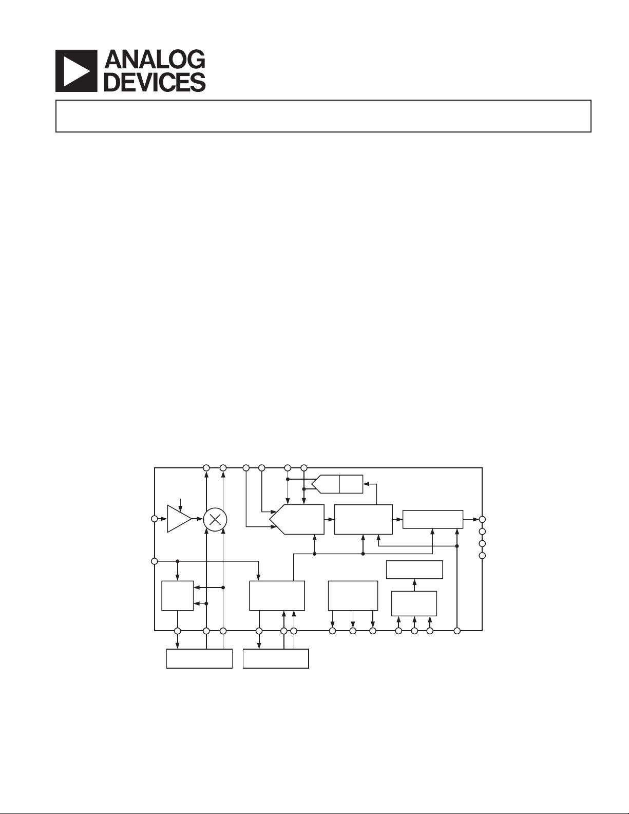
The AD9874 is a general-purpose IF subsystem that digitizes a
low level 10 MHz to 300 MHz IF input with a signal bandwidth
ranging from 6.8 kHz to 270 kHz. The signal chain of the AD9874
consists of a low noise amplifier, a mixer, a band-pass sigma-delta
analog-to-digital converter, and a decimation filter with programmable decimation factor. An automatic gain control (AGC) circuit
gives the AD9874 12 dB of continuous gain adjustment. Auxiliary blocks include both clock and LO synthesizers.
The AD9874’s high dynamic range and inherent antialiasing
provided by the band-pass sigma-delta converter allow the
AD9874
to cope with blocking signals up to 95 dB stronger
than the desired signal. This attribute can often reduce the cost of
a
radio by reducing its IF filtering requirements. Also, it enables
multimode radios of varying channel bandwidths, allowing the
IF filter to be specified for the largest channel bandwidth.
The SPI port programs numerous parameters of the AD9874,
thus allowing the device to be optimized for any given application.
Programmable parameters include synthesizer divide ratios, AGC
attenuation and attack/decay time, received signal strength level,
decimation factor, output data format, 16 dB attenuator, and the
selected bias currents. The bias currents of the LNA and mixer
can be further reduced at the expense of degraded performance
for battery-powered applications.
FUNCTIONAL BLOCK DIAGRAM
MXOP MXON IF2P IF2N GCP GCN
–16dB
IFIN
FREF
*Protected by U.S. Patent No. 5,969,657; other patents pending.
LNA
LO
SYN
LO VCO AND
LOOP FILTER
⌺-⌬ ADC
CLK SYN
CLKNCLKPIOUTCLONLOPIOUTL
LOOP FILTER
REV. A
Information furnished by Analog Devices is believed to be accurate and
reliable. However, no responsibility is assumed by Analog Devices for its
use, nor for any infringements of patents or other rights of third parties that
may result from its use. No license is granted by implication or otherwise
under any patent or patent rights of Analog Devices. Trademarks and
registered trademarks are the property of their respective companies.
DAC AGC
DECIMATION
FILTER
VOLTA G E
REFERENCE
One Technology Way, P.O. Box 9106, Norwood, MA 02062-9106, U.S.A.
Tel: 781/329-4700 www.analog.com
Fax: 781/326-8703 © 2003 Analog Devices, Inc. All rights reserved.
AD9874
FORMATTING/SSI
CONTROL LOGIC
SPI
DOUTA
DOUTB
FS
CLKOUT
SYNCBPEPDPCVREFNVCMVREFP

AD9874
TABLE OF CONTENTS
AD9874—SPECIFICATIONS . . . . . . . . . . . . . . . . . . . . . . . 3
ABSOLUTE MAXIMUM RATINGS . . . . . . . . . . . . . . . . . 5
PIN CONFIGURATION/DESCRIPTION . . . . . . . . . . . . . 6
DEFINITION OF SPECIFICATIONS/
TEST METHODS . . . . . . . . . . . . . . . . . . . . . . . . . . . . . . 7
TYPICAL PERFORMANCE CHARACTERISTICS . . . . . 8
SERIAL PERIPHERAL INTERFACE (SPI) . . . . . . . . . . . 13
SYNCHRONOUS SERIAL INTERFACE (SSI) . . . . . . . . 16
Synchronization Using SYNCB . . . . . . . . . . . . . . . . . . . . 18
Interfacing to DSPs . . . . . . . . . . . . . . . . . . . . . . . . . . . . . 18
POWER CONTROL . . . . . . . . . . . . . . . . . . . . . . . . . . . . . 19
LO SYNTHESIZER . . . . . . . . . . . . . . . . . . . . . . . . . . . . . . 19
Fast Acquire Mode . . . . . . . . . . . . . . . . . . . . . . . . . . . . . 20
CLOCK SYNTHESIZER . . . . . . . . . . . . . . . . . . . . . . . . . . 21
IF LNA/MIXER . . . . . . . . . . . . . . . . . . . . . . . . . . . . . . . . . 22
BAND-PASS SIGMA DELTA (⌺-⌬) ADC . . . . . . . . . . . . 24
DECIMATION FILTER . . . . . . . . . . . . . . . . . . . . . . . . . . 26
VARIABLE GAIN AMPLIFIER WITH AGC . . . . . . . . . . 28
Variable Gain Control . . . . . . . . . . . . . . . . . . . . . . . . . . . 28
Automatic Gain Control . . . . . . . . . . . . . . . . . . . . . . . . . 29
System NF vs. VGA Control . . . . . . . . . . . . . . . . . . . . . . 31
APPLICATION CONSIDERATIONS . . . . . . . . . . . . . . . 32
Frequency Planning . . . . . . . . . . . . . . . . . . . . . . . . . . . . . 32
Spurious Responses . . . . . . . . . . . . . . . . . . . . . . . . . . . . . 33
EXTERNAL PASSIVE COMPONENT
REQUIREMENTS . . . . . . . . . . . . . . . . . . . . . . . . . . . . . 34
APPLICATIONS . . . . . . . . . . . . . . . . . . . . . . . . . . . . . . . . 34
Superheterodyne Receiver . . . . . . . . . . . . . . . . . . . . . . . . 34
Synchronization of Multiple AD9874s . . . . . . . . . . . . . . . 36
Split Path Rx Architecture . . . . . . . . . . . . . . . . . . . . . . . . 37
Hung Mixer Mode . . . . . . . . . . . . . . . . . . . . . . . . . . . . . . 38
LAYOUT EXAMPLE
EVALUATION BOARD AND SOFTWARE . . . . . . . . . 38
OUTLINE DIMENSIONS . . . . . . . . . . . . . . . . . . . . . . . . . 39
REVISION HISTORY . . . . . . . . . . . . . . . . . . . . . . . . . . . . 40
–2–
REV. A

AD9874–SPECIFICATIONS
VDDQ = VDDP = 2.7 V to 5.5 V, f
= 18 MSPS, fIF = 109.65 MHz, fLO = 107.4 MHz, f
CLK
(VDDI = VDDF = VDDA = VDDC = VDDL = VDDD = VDDH = 2.7 V to 3.6 V,
= 16.8 MHz, unless otherwise noted.)
REF
1
Parameter Temp Test Level Min Typ Max Unit
3, 4
2
3, 4
Full IV 8.1 9.5 dB
Full IV 13 dB
3
Full IV 91 95 dB
Full IV –20 –19 dBm
Full IV –32 –31 dBm
SYSTEM DYNAMIC PERFORMANCE
SSB Noise Figure @ Min VGA Attenuation
@ Max VGA Attenuation
3, 4
Dynamic Range with AGC Enabled
IF Input Clip Point @ Max VGA Attenuation
@ Min VGA Attenuation
3
Input Third Order Intercept (IIP3) Full IV –5 0 dBm
Gain Variation over Temperature Full IV 0.7 2 dB
LNA + MIXER
Maximum RF and LO Frequency Range Full IV 300 500 MHz
LNA Input Impedance 25
o
CV 370//1.4 ⍀//pF
Mixer LO Input Resistance 25oCV 1 k⍀
LO SYNTHESIZER
LO Input Frequency Full IV 7.75 300 MHz
LO Input Amplitude Full IV 0.3 2.0 V p-p
FREF Frequency (for Sinusoidal Input ONLY) Full IV 8 25 MHz
FREF Input Amplitude Full IV 0.3 3 V p-p
FREF Slew Rate Full IV 7.5 V/s
Minimum Charge Pump Current
Maximum Charge Pump Current
Charge Pump Output Compliance
@
@
5
5 V
5
5 V
6
Full VI 0.48 0.67 0.78 mA
Full VI 3.87 5.3 6.2 mA
Full VI 0.4 VDDP – 0.4 V
Synthesizer Resolution Full IV 6.25 kHz
CLOCK SYNTHESIZER
CLK Input Frequency Full IV 13 26 MHz
CLK Input Amplitude Full IV 0.3 VDDC V p-p
Minimum Charge Pump Output Current
Maximum Charge Pump Output Current
Charge Pump Output Compliance
5
5
6
Full VI 0.48 0.67 0.78 mA
Full VI 3.87 5.3 6.2 mA
Full VI 0.4 VDDQ – 0.4 V
Synthesizer Resolution Full IV 2.2 kHz
SIGMA-DELTA ADC
Resolution Full IV 16 24 Bits
Clock Frequency (f
Center Frequency Full V f
Pass-Band Gain Variation Full IV 1.0 dB
) Full IV 13 26 MHz
CLK
/8 MHz
CLK
Alias Attenuation Full IV 80 dB
GAIN CONTROL
Programmable Gain Step Full V 16 dB
AGC Gain Range (Continuous) Full V 12 dB
GCP Output Resistance Full IV 50 72.5 95 k⍀
OVERALL
Analog Supply Voltage
(VDDA, VDDF, VDDI) Full VI 2.7 3.0 3.6 V
Digital Supply Voltage
(VDDD, VDDC, VDDL) Full VI 2.7 3.0 3.6 V
Interface Supply Voltage
7
(VDDH) Full VI 1.8 3.6 V
Charge Pump Supply Voltage
(VDDP, VDDQ) Full VI 2.7 5.0 5.5 V
Total Current
High Performance Setting
Low Power Mode
8
8
Full VI 20 26.5 mA
Full VI 17 22 mA
Standby Full VI 0.01 0.1 mA
OPERATING TEMPERATUR
NOTES
1
Standard operating mode: LNA/Mixer @ high bias setting, VGA @ Min ATTEN setting, synthesizers in normal (not fast acquire) mode, f
factor = 900, 16-bit digital output, and 10 pF load on SSI output pins.
2
This includes 0.9 dB loss of matching network.
3
AGC with DVGA enabled.
4
Measured in 10 kHz bandwidth.
5
Programmable in 0.67 mA steps.
6
Voltage span in which LO (or CLK) charge pump output current is maintained within 5% of nominal value of VDDP/2 (or VDDQ/2).
7
VDDH must be less than VDDD + 0.5 V.
8
Clock VCO off, add additional 0.7 mA with VGA @ Max ATTEN setting.
Specifications subject to change without notice.
REV. A
E RANGE –40 +85 °C
= 18 MHz, decimation
CLK
–3–

AD9874
DIGITAL SPECIFICATIONS
f
= 18 MSPS, fIF = 109.65 MHz, fLO = 107.4 MHz, f
CLK
(VDDI = VDDF = VDDA = VDDC = VDDL = VDDD = VDDH = 2.7 V to 3.6 V, VDDQ = VDDP = 2.7 V to 5.5 V,
= 16.8 MHz, unless otherwise noted.)
REF
1
Parameter Temp Test Level Min Typ Max Unit
DECIMATOR
Decimation Factor
Pass-Band Width Full V 50% f
2
Full IV 48 960
CLKOUT
Pass-Band Gain Variation Full IV 1.2 dB
Alias Attenuation Full IV 88 dB
SPI-READ OPERATION (See Figure 1a)
PC Clock Frequency Full IV 10 MHz
PC Clock Period (t
PC Clock HI (t
PC Clock LOW (t
PC to PD Setup Time (t
PC to PD Hold Time (t
PE to PC Setup Time (t
) Full IV 100 ns
CLK
) Full IV 45 ns
HI
) Full IV 45 ns
LOW
) Full IV 2 ns
DS
) Full IV 2 ns
DH
) Full IV 5 ns
S
PC to PE Hold Time (tH) Full IV 5 ns
SPI-WRITE OPERATION
3
(See Figure 1b)
PC Clock Frequency Full IV 10 MHz
PC Clock Period (t
PC Clock HI (t
PC Clock LOW (t
PC to PD Setup Time (t
PC to PD Hold Time (t
PC to PD (or DOUBT) Data Valid Time (t
) Full IV 100 ns
CLK
) Full IV 45 ns
HI
) Full IV 45 ns
LOW
) Full IV 2 ns
DS
) Full IV 2 ns
DH
) Full IV 3 ns
DV
PE to PD Output Valid to Hi-Z (tEZ) Full IV 8 ns
3
(see Figure 2b)
SSI
CLKOUT Frequency Full IV 0.867 26 MHz
CLKOUT Period (t
CLKOUT Duty Cycle (t
CLKOUT to FS Valid Time (t
) Full IV 38.4 1153 ns
CLK
) Full IV 33 50 67 ns
HI, tLOW
) Full IV –1 +1 ns
V
CLKOUT to DOUT Data Valid Time (tDV) Full IV –1 +1 ns
CMOS LOGIC INPUTS
4
Logic “1” Voltage (VIH) Full IV VDDH – 0.2 V
Logic “0” Voltage (V
Logic “1” Current (V
Logic “0” Current (V
) Full IV 0.5 V
IL
) Full IV 10 µA
IH
) Full IV 10 µA
IL
Input Capacitance Full IV 3 pF
CMOS LOGIC OUTPUTS
3, 4, 5
Logic “1” Voltage (VIH) Full IV VDDH – 0.2 V
Logic “0” Voltage (VIL) Full IV 0.2 V
NOTES
1
Standard operating mode: high IIP3 setting, synthesizers in normal (not fast acquire) mode, f
VDDx = 3.0 V.
2
Programmable in steps of 48 or 60.
3
CMOS output mode with C
4
Absolute Max and Min input/output levels are VDDH +0.3 V and –0.3 V.
5
IOL = 1 mA; specification is also dependent on Drive Strength setting.
Specifications subject to change without notice.
= 10 pF and Drive Strength = 7.
LOAD
= 18 MHz, decimation factor = 300, 10 pF load on SSI output pins:
CLK
–4–
REV. A
AD9874
ABSOLUTE MAXIMUM RATINGS*
Parameter With Respect to Min Max Unit
VDDF, VDDA, VDDC, VDDD, VDDH, GNDF, GNDA, GNDC, GNDD, GNDH, –0.3 +4.0 V
VDDL, VDDI GNDL, GNDI, GNDS
VDDF, VDDA, VDDC, VDDD, VDDH, VDDR, VDDA, VDDC, VDDD, VDDH, –4.0 +4.0 V
VDDL, VDDI VDDL, VDDI
VDDP, VDDQ GNDP, GNDQ –0.3 +6.0 V
GNDF, GNDA, GNDC, GNDD, GNDH, GNDF, GNDA, GNDC, GNDD, GNDH, –0.3 +0.3 V
GNDL, GNDI, GNDQ, GNDP, GNDS GNDL, GNDI, GNDQ, GNDP, GNDS
MXOP, MXON, LOP, LON, IFIN, GNDI –0.3 VDDI + 0.3 V
CXIF, CXVL, CXVM
PC, PD, PE, CLKOUT, DOUTA, GNDH –0.3 VDDH + 0.3 V
DOUTB, FS, SYNCB
IF2N, IF2P, GCP, GCN GNDF –0.3 VDDF + 0.3 V
VREFP, VREFN, RREF GNDA –0.3 VDDA + 0.3 V
IOUTC GNDQ –0.3 VDDQ + 0.3 V
IOUTL GNDP –0.3 VDDP + 0.3 V
CLKP, CLKN GNDC –0.3 VDDC + 0.3 V
FREF GNDL –0.3 VDDL + 0.3 V
Junction Temperature 150 °C
Storage Temperature –65 +150 °C
Lead Temperature (10 sec) 300 °C
*Stresses above those listed under Absolute Maximum Ratings may cause permanent damage to the device. This is a stress rating only; functional operation of the
device at these or any other conditions above those indicated in the operational sections of this specification is not implied. Exposure to absolute maximum ratings for
extended periods may affect device reliability.
THERMAL CHARACTERISTICS
Thermal Resistance
48-Lead LQFP
= 76.2°C/W
JA
= 17°C/W
JC
EXPLANATION OF TEST LEVELS
TEST LEVEL
I. 100% production tested.
II. 100% production tested at 25°C and sample tested at
specified temperatures. AC testing done on sample basis.
III. Sample tested only.
IV. Parameter is guaranteed by design and/or
characterization testing.
V. Parameter is a typical value only.
VI. All devices are 100% production tested at 25°C; min and
max guaranteed by design and characterization for industrial
temperature range.
ORDERING GUIDE
Model Temperature Range Package Description Package Option
AD9874ABST –40°C to +85°C 48-Lead Thin Plastic Quad Flatpack (LQFP) ST-48
AD9874EB Evaluation Board
CAUTION
ESD (electrostatic discharge) sensitive device. Electrostatic charges as high as 4000 V readily
accumulate on the human body and test equipment and can discharge without detection. Although the
AD9874 features proprietary ESD protection circuitry, permanent damage may occur on devices
subjected to high energy electrostatic discharges. Therefore, proper ESD precautions are recommended
to avoid performance degradation or loss of functionality.
REV. A
–5–
AD9874
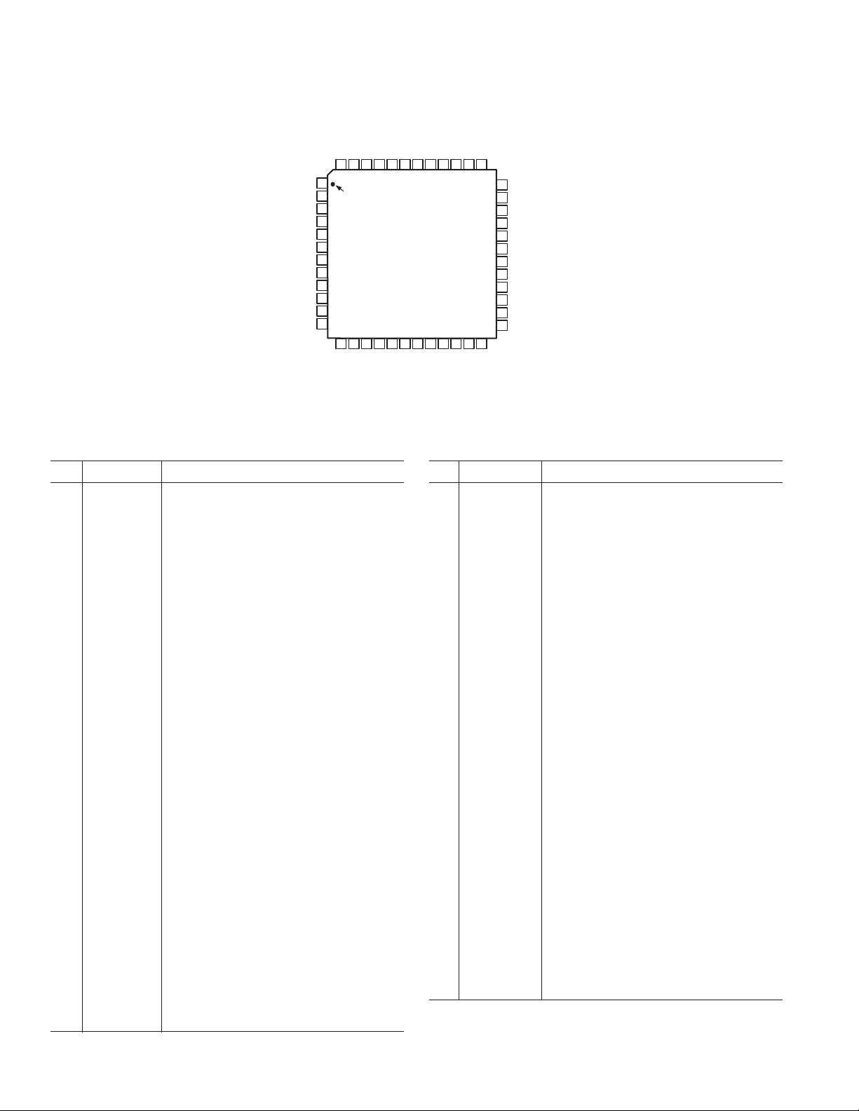
PIN CONFIGURATION
VDDI
IFIN
CXIF
GNDI
CXVL
LOP
LON
CXVM
VDDL
VDDP
IOUTL
CLKP
GNDC
404142
CLKN
GNDS
GNDD
PC
MXOP
MXON
GNDF
IF2N
IF2P
VDDF
GCP
GCN
VDDA
GNDA
VREFP
VREFN
48 47 46 45 44 39 38 3743
1
PIN 1
2
IDENTIFIER
3
4
5
6
7
8
9
10
11
12
13 191817161514 20 21 22 23 24
RREF
VDDQ
IOUTC
AD9874
TOP VIEW
(Not to Scale)
VDDC
GNDQ
PIN FUNCTION DESCRIPTIONS
GNDP
PD
36
35
34
33
32
31
30
29
28
27
26
25
GNDL
FREF
GNDS
SYNCB
GNDH
FS
DOUTB
DOUTA
CLKOUT
VDDH
VDDD
PE
Pin Mnemonic Description
1 MXOP Mixer Output, Positive.
2MXON Mixer Output, Negative.
3 GNDF Ground for Front End of ADC.
4IF2N Second IF Input (to ADC), Negative.
5 IF2P Second IF Input (to ADC), Positive.
6 VDDF Positive
Power Supply for Front End of ADC.
7 GCP Filter Capacitor for ADC Full-Scale Control.
8 GCN Full-Scale Control Ground.
9 VDDA Positive Power Supply for ADC Back End.
10 GNDA Ground for ADC Back End.
11 VREFP Voltage Reference, Positive.
12 VREFN Voltage Reference, Negative.
13 RREF Reference Resistor: Requires 100 kΩ to
GNDA.
14 VDDQ Positive
Power Supply for Clock Synthesizer.
15 IOUTC Clock Synthesizer Charge Pump Output
Current.
16 GNDQ Ground for Clock Synthesizer Charge
Pump.
17 VDDC Positive
Power Supply for Clock Synthesizer.
18 GNDC Ground for Clock Synthesizer.
19 CLKP Sampling Clock Input/Clock VCO Tank,
Positive.
20 CLKN Sampling Clock Input/Clock VCO Tank,
Negative.
21 GNDS Substrate Ground.
22 GNDD Ground for Digital Functions.
23 PC Clock Input for SPI Port.
24 PD Data I/O for SPI Port.
25 PE Enable Input for SPI Port.
26 VDDD Positive Power Supply for Internal Digital
Function.
Pin Mnemonic Description
27 VDDH Positive Power Supply for Digital Interface.
28 CLKOUT Clock Output for SSI Port.
29 DOUTA Data Output for SSI Port.
30 DOUTB Data Output for SSI Port (Inverted) or
SPI Port.
31 FS Frame Sync for SSI Port.
32 GNDH Ground for Digital Interface.
33 SYNCB Resets SSI and Decimator Counters;
Active Low.
34 GNDS Substrate Ground.
35 FREF Reference Frequency Input for Both
Synthesizers.
36 GNDL Ground for LO Synthesizer.
37 GNDP Ground for LO Synthesizer Charge Pump.
38 IOUTL LO Synthesizer Charge Pump Output
Current Charge Pump.
39 VDDP Positive Power Supply for LO Synthesizer
Charge Pump.
40 VDDL Positive Power Supply for LO Synthesizer.
41 CXVM External Filter Capacitor; DC Output of
LNA.
42 LON LO Input to Mixer and LO Synthesizer,
Negative.
43 LOP LO Input to Mixer and LO Synthesizer,
Positive.
44 CXVL External Bypass Capacitor for LNA Power
Supply.
45 GNDI Ground for Mixer and LNA.
46 CXIF External Capacitor for Mixer V-I Con-
verter Bias.
47 IFIN First IF Input (to LNA).
48 VDDI Positive Power Supply for LNA and Mixer.
–6–
REV. A

AD9874
DEFINITION OF SPECIFICATIONS/TEST METHODS
Single-Sideband Noise Figure (SSB NF)
Noise figure (NF) is defined as the degradation in SNR performance (in dB) of an IF input signal after it passes through a
component or system. It can be expressed with the equation
Noise Figure SNR SNR
=×10 log( )
IN OUT
The term SSB is applicable for heterodyne systems containing a
mixer. It indicates that the desired signal spectrum resides on
only one side of the LO frequency (i.e., single sideband); thus a
“noiseless” mixer has a noise figure of 3 dB.
The AD9874’s SSB noise figure is determined by the equation
SSB NF P BW dBm Hz SNR
=−×
{}
IN
()
−−10 174log
where PIN is the input power of an unmodulated carrier, BW is
the noise measurement bandwidth, –174 dBm/Hz is the thermal
noise floor at 293 K, and SNR is the measured signal-to-noise
ratio in dB of the AD9874.
Note that P
is set to –85 dBm to minimize any degradation in
IN
measured SNR due to phase noise from the RF and LO signal
generators. The IF frequency, CLK frequency, and decimation
factors are selected to minimize any spurious components
falling within the measurement bandwidth. Note also that a
bandwidth of 10 kHz is used for the data sheet specification.
Refer to Figures 22a and 22b for an indication of how NF varies
with BW. Also, refer to the TPCs to see how NF is affected by
different operating conditions. All references to noise figures
within this data sheet imply single-sideband noise figure.
Input Third Order Intercept (IIP3)
IIP3 is a figure of merit used to determine a component’s or
system’s susceptibility to intermodulation distortion (IMD)
from its third order nonlinearities. Two unmodulated carriers at
a specified frequency relationship (f
and f2) are injected into a
1
nonlinear system exhibiting third order nonlinearities producing
IMD components at 2f
– f2 and 2f2 – f1. IIP3 graphically repre-
1
sents the extrapolated intersection of the carrier’s input power
with the third order IMD component when plotted in dB. The
difference in power (D in dBc) between the two carriers and the
resulting third order IMD components can be determined from
the equation
D IIP P
=×23(–)
IN
Dynamic Range (DR)
Dynamic range is the measure of a small target input signal
(P
(P
) in the presence of a large unwanted interferer signal
TARGET
). Typically, the large signal will cause some unwanted
INTER
characteristic of the component or system to degrade, thus
making it unable to detect the smaller target signal correctly. In
the case of the AD9874, it is often a degradation in noise figure
at increased VGA attenuation settings that limits its dynamic
range (refer to TPCs 15a, 15b, and 15c).
The test method for the AD9874 is as follows. The small target
signal (an unmodulated carrier) is input at the center of the IF
frequency, and its power level (P
SNR
of 6 dB. The power of the signal is then increased by
TARGET
) is adjusted to achieve an
TARGET
3 dB prior to injecting the interferer signal. The offset frequency
of the interferer signal is selected so that aliases produced by
the decimation filter’s response as well as phase noise from the LO
(due to reciprocal mixing) do not fall back within the measurement
bandwidth. For this reason, an offset of 110 kHz was selected.
The interferer signal (also an unmodulated carrier) is then
injected into the input and its power level is increased to the
point (P
) where the target signal SNR is reduced to 6 dB.
INTER
The dynamic range is determined with the equation:
DR P P SNR
=+–
INTER TARGET TARGET
Note that the AD9874’s AGC is enabled for this test.
IF Input Clip Point
The IF input clip point is defined as 2 dB below the input power
level (P
), resulting in the clipping of the AD9874’s ADC.
IN
Unlike other linear components that typically exhibit a soft
compression (characterized by its 1 dB compression point), an
ADC exhibits a hard compression once its input signal exceeds
its rated maximum input signal range. In the case of the AD9874,
which contains a - ADC, hard compression should be avoided
because it causes severe SNR degradation.
REV. A
–7–
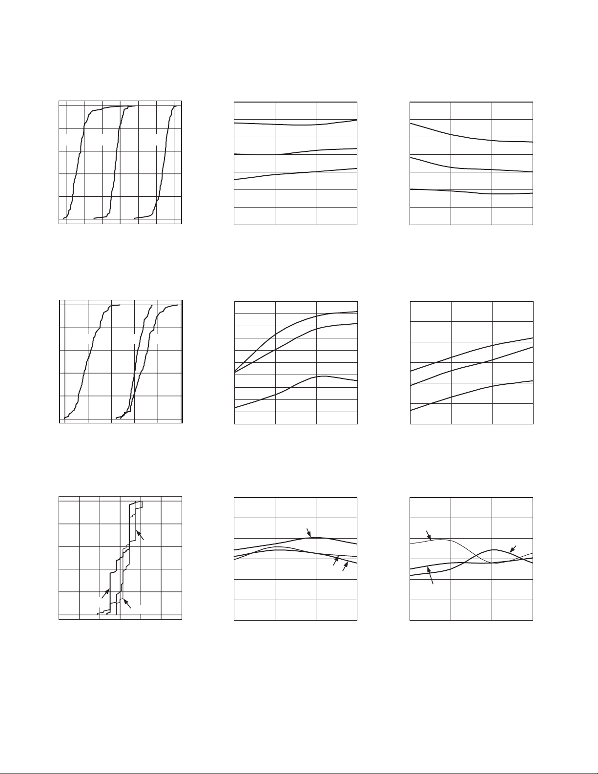
AD9874–Typical Performance Characteristics
(VDDI = VDDF = VDDA = VDDC = VDDL = VDDD = VDDH = VDDx, VDDQ = VDDP = 5.0 V,
f
= 18 MSPS,
CLK
f
= 109.56 MHz,
IF
f
LO
TA = 25C, LO = –5 dBm, LO and CLK Synthesizer Disabled, 16-Bit Data with AGC and DVGA enabled, unless otherwise noted.)
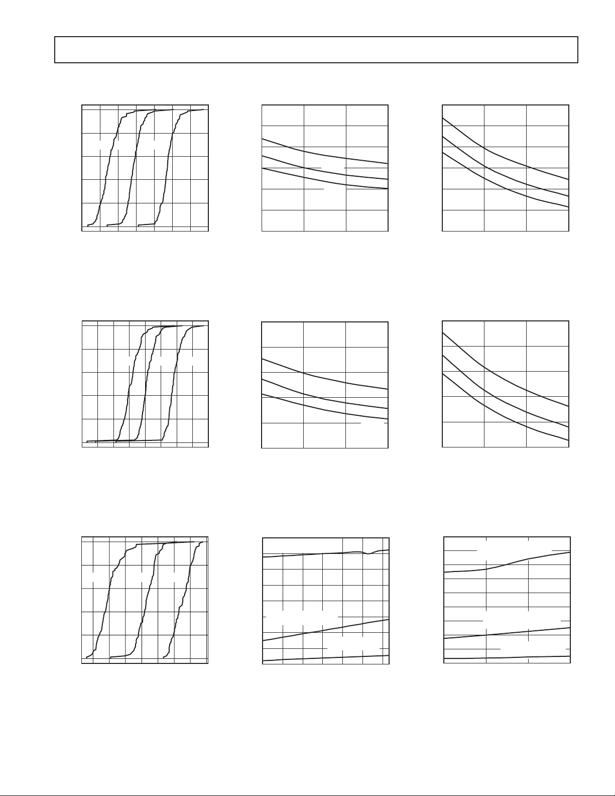
100
80
–40C +25C +85C
60
40
PERCENTAGE – %
20
0
7.5 7.8 8.1 8.4 8.7 9.0
7.2
TPC 1a. CDF of SSB Noise Figure
(VDDx = 3.0 V, High Bias
100
80
60
40
PERCENTAGE – %
20
0
–3
TPC 2a. CDF of IIP3 (VDDx = 3.0 V,
High Bias
NOISE FIGURE – dB
2
)
–40C +25C +85C
–2 –1 0 1 2
IIP3 – dBm
2
)
9.5
9.0
8.5
8.0
7.5
NF – dB
7.0
6.5
6.0
2.7
TPC 1b. SSB Noise Figure vs. Supply
(High Bias
1.5
1.0
0.5
–0.5
–1.0
–1.5
IIP3 – dBm
–2.0
–2.5
–3.0
–3.5
0
2.7
2
)
+85C
+25C
–40C
3.0 3.3 3.6
VDDx – V
+85C
+25C
–40C
3.0 3.3 3.6
VDDx – V
TPC 2b. IIP3 vs. Supply (High Bias2)
9.5
9.0
8.5
8.0
7.5
NF – dB
7.0
6.5
6.0
2.7
TPC 1c. SSB Noise Figure vs. Supply
(Low Bias
0
–2
–4
–6
IIP3 – dBm
–8
–10
–12
2.7
3.0 3.3 3.6
3
)
3.0 3.3 3.6
TPC 2c. IIP3 vs. Supply (Low Bias3)
= 107.4 MHz,
1
+85C
+25C
–40C
VDDx – V
+85C
+25C
–40C
VDDx – V
100
80
+25C
2
–40C
)
60
40
PERCENTAGE – %
20
+85C
0
93 94 95 96 97 98
92
DYNAMIC RANGE – dB
TPC 3a. CDF of Dynamic Range
(VDDx = 3.0 V, High Bias
1
Data taken with Toko FSLM series 10 µH inductors.
2
High Bias corresponds to LNA_Mixer Setting of 33 in SPI Register 0x01.
3
Low Bias corresponds to LNA_Mixer Setting of 12 in SPI Register 0x01.
98
97
96
95
DR – dB
94
93
92
2.7
TPC 3b. Dynamic Range vs. Supply
(High Bias
2
)
–40C
+85C
+25C
3.0 3.3 3.6
VDDx – V
–8–
98
97
+25C
96
95
DR – dB
94
+85C
93
92
2.7
TPC 3c. Dynamic Range vs. Supply
(Low Bias
3.0 3.3 3.6
VDDx – V
3
)
–40C
REV. A
AD9874
(VDDI = VDDF = VDDA = VDDC = VDDL = VDDD = VDDH = VDDx, VDDQ = VDDP = 5.0 V,
f
= 18 MSPS,
CLK
f
= 109.56 MHz,
IF
f
LO
TA = 25ⴗC, LO = –5 dBm, LO and CLK Synthesizer Disabled, 16-Bit Data with AGC and DVGA enabled, unless otherwise noted.)
100
80
+25ⴗC +85ⴗC–40ⴗC
60
40
PERCENTAGE – %
20
0
–19.4 –19.2 –19.0 –18.8 –18.6 –18.4
IFIN CLIP POINT – dBm
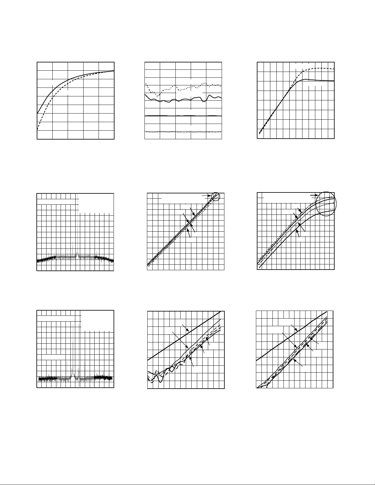
TPC 4a. CDF of Maximum VGA
Attenuation Clip Point (VDDx = 3.0 V,
High Bias
100
80
60
40
PERCENTAGE – %
20
0
2
)
+25ⴗC +85ⴗC–40ⴗC
–31.6
–31.4 –31.2 –31.0 –30.8 –30.6 –30.4
IFIN CLIP POINT – dBm
TPC 5a. CDF of Minimum VGA
Attenuation Clip Point (VDDx = 3.0 V,
High Bias
2
)
–17.5
–18.0
–18.5
–19.0
–19.5
INPUT CLIP POINT – dBm
–20.0
–20.5
2.7 3.0 3.3 3.6
+85ⴗC
+25ⴗC
–40ⴗC
VDDx – V
TPC 4b. Maximum VGA Attenuation
Clip Point vs. Supply (High Bias2)
–29.5
–30.0
–30.5
+85ⴗC
–31.0
INPUT CLIP POINT – dBm
–31.5
–32.0
2.7
3.0 3.3 3.6
VDDx – V
+25ⴗC
–40ⴗC
TPC 5b. Minimium VGA Attenuation
Clip Point vs. Supply (High Bias2)
–17.5
–18.0
–18.5
–19.0
–19.5
INPUT CLIP POINT – dBm
–20.0
–20.5
2.7
TPC 4c. Maximum VGA Attenuation
Clip Point vs. Supply (Low Bias
–29.5
–30.0
–30.5
–31.0
INPUT CLIP POINT – dBm
–31.5
–32.0
2.7
TPC 5c. Minimium VGA Attenuation
Clip Point vs. Supply (Low Bias3)
= 107.4 MHz,
1
+85ⴗC
+25ⴗC
–40ⴗC
3.0 3.3 3.6
VDDx – V
3
)
+85ⴗC
+25ⴗC
–40ⴗC
3.0 3.3 3.6
VDDx – V
100
80
–40ⴗC
60
40
PERCENTAGE – %
20
0
18.5
19.0 19.5 20.0 20.5 21.0 21.5 22.0
SUPPLY CURRENT – mA
TPC 6a. CDF of Supply Current
(VDDx = 3.0 V, High Bias
1
Data taken with Toko FSLM series 10 µH inductors.
2
High Bias corresponds to LNA_Mixer Setting of 33 in SPI Register 0x01.
3
Low Bias corresponds to LNA_Mixer Setting of 12 in SPI Register 0x01.
+85ⴗC+25ⴗC
2
)
16
(IDDA, IDDF, AND IDDI)
14
12
10
8
6
4
SUPPLY CURRENT – mA
2
0
13
DIGITAL
(IDDD, IDDC, AND IDDL)
15 17 19 21 23 25
TPC 6b. Supply Current vs. f
(VDDx = 3.0 V, High Bias2)
REV. A
ANALOG
f
CLK
–9–
DIGITAL INTERFACE
(IDDH)
– MHz
CLK
18
16
14
12
10
8
6
SUPPLY CURRENT – mA
4
2
0
2.7
TPC 6c. Supply Current vs. Supply
(High Bias
2
ANALOG
(IDDA, IDDF, AND IDDI)
DIGITAL
(IDDD, IDDC, AND IDDL)
DIGITAL INTERFACE
(IDDH)
3.0 3.3 3.6
VDDx – V
)
AD9874
IFIN – dBm
IMD – dBc
–55
–109
–61
–67
–73
–85
–91
–103
–51 –48 –45 –42 –39 –36 –33 –30
PIN
2.7V
3.6V
3.0V
3.3V
–115
–97
–79
PIN – dBFS
–15
–42
–18
–21
–24
–30
–33
–39
–45
–36
–27
(VDDI = VDDF = VDDA = VDDC = VDDL = VDDD = VDDH = VDDx, VDDQ = VDDP = 5.0 V,
f
= 18 MSPS,
CLK
f
= 109.56 MHz,
IF
f
LO
TA = 25ⴗC, LO = –5 dBm, LO and CLK Synthesizer Disabled, 16-Bit Data with AGC and DVGA enabled, unless otherwise noted.)
0.1
0
–0.1
LOW BIAS
GAIN VARIATION – dB
–0.2
–0.3
–0.4
–0.5
–0.6
–0.7
–0.8
–20
HIGH BIAS
–14 –8 –5
LO DRIVE – dBm
–11–17
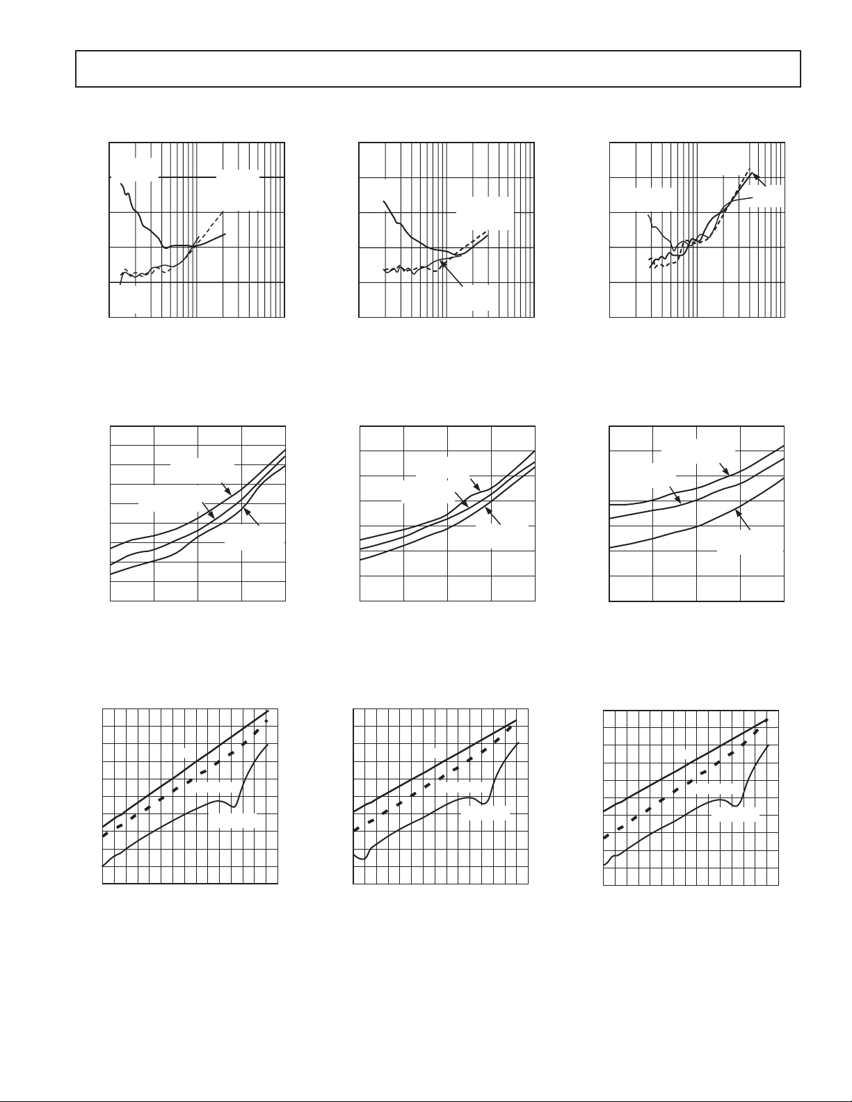
TPC 7a. Normalized Gain Variation
vs. LO Drive (VDDx = 3.0 V)
0
–2.8dBFS OUTPUT
–20
–40
–60
dBFS
–80
–100
–120
–140
–80 –60 –40 –20 0 20 40 60
FREQUENCY – kHz
NBW = 3.66kHz
= 18MHz
f
CLK
MAX VGA ATTEN
DEC–BY–120
TPC 8a. Complex FFT of Baseband
I/Q for Single-Tone (High Bias)
9.0
8.8
8.6
8.4
8.2
8.0
7.8
7.6
NOISE FIGURE – dBc
7.4
7.2
7.0
–20
NF-HIGH BIAS
NF-LOW BIAS
IMD-LOW BIAS
IMD-HIGH BIAS
–10 0 5
LO DRIVE – dBm
–5–15
TPC 7b. Noise Figure and IMD
vs. LO Drive (VDDx = 3.0 V)
0
–2
–4
–6
dBFS
–8
–10
–12
–14
80
–30
TPC 8b. Gain Compression vs. IFIN
(High Bias
ADC GOES INTO
HARD COMPRESSION
–28 –26 –24 –22 –20 –18 –16
2
)
3.6V
3.3V
3.0V
2.7V
IFIN – dBm
0
–10
–20
–30
–40
–50
–60
–70
–80
–12
–15
–18
–21
–24
dBm
–27
–30
IMD w/ IFIN = –36 dBm – dBc
–33
–36
–36
TPC 7c. Gain Compression vs. IFIN
with 16 dB LNA Attenuator Enabled
0
–2
–4
–6
dBFS
–8
–10
–12
–14
–30
TPC 8c. Gain Compression vs. IFIN
(Low Bias3)
–30 –24 –18 –12 –6 0
ADC DOES NOT GO INTO
HARD COMPRESSION
–28 –26 –24 –22 –20 –18 –14
= 107.4 MHz,
1
HIGH BIAS
LOW BIAS
IFIN – dBm
3.6V
3.3V
3.0V
2.7V
–16
IFIN – dBm
0
–18.2dBFS OUTPUT
–20
–40
–60
dBFS
–80
IMD = 74dBc
–100
–120
–140
–80 –60 –40 –20 0 20 40 60
TPC 9a. Complex FFT of Baseband
I/Q for Dual Tone IMD (High Bias
with Each IFIN Tone @ –35 dBm)
1
Data taken with Toko FSLM series 10 µH inductors.
2
High Bias corresponds to LNA_Mixer Setting of 33 in SPI Register 0x01.
3
Low Bias corresponds to LNA_Mixer Setting of 12 in SPI Register 0x01.
FREQUENCY – kHz
NBW = 3.66kHz
f
= 18MHz
CLK
MAX VGA ATTEN
DEC–BY–120
–70
–76
–82
–88
–94
–100
–106
IMD – dBc
–112
–118
–124
80
–130
–51 –48 –45 –42 –39 –36 –33 –30
PIN
2.7V
3.3V
3.6V
IFIN – dBm
TPC 9b. IMD vs. IFIN (High Bias2)
–10–
3.0V
–15
–18
–21
–24
–27
–30
–33
PIN – dBFS
–36
–39
–42
–45
TPC 9c. IMD vs. IFIN (Low Bias3)
REV. A
AD9874
(VDDI = VDDF = VDDA = VDDC = VDDL = VDDD = VDDH = VDDx, VDDQ = VDDP = 5.0 V,
f
= 18 MSPS,
CLK
f
= 109.56 MHz,
IF
f
L
O
TA = 25ⴗC, LO = –5 dBm, LO and CLK Synthesizer Disabled, 16-Bit Data with AGC and DVGA enabled, unless otherwise noted.)
10.0
16-BIT
I/Q DATA
9.5
9.0
8.5
NOISE FIGURE – dB
8.0
24-BIT
I/Q DATA
7.5
10
CHANNEL BANDWIDTH – kHz
16-BIT
I/Q DATA
w/ DVGA
ENABLED
1000100
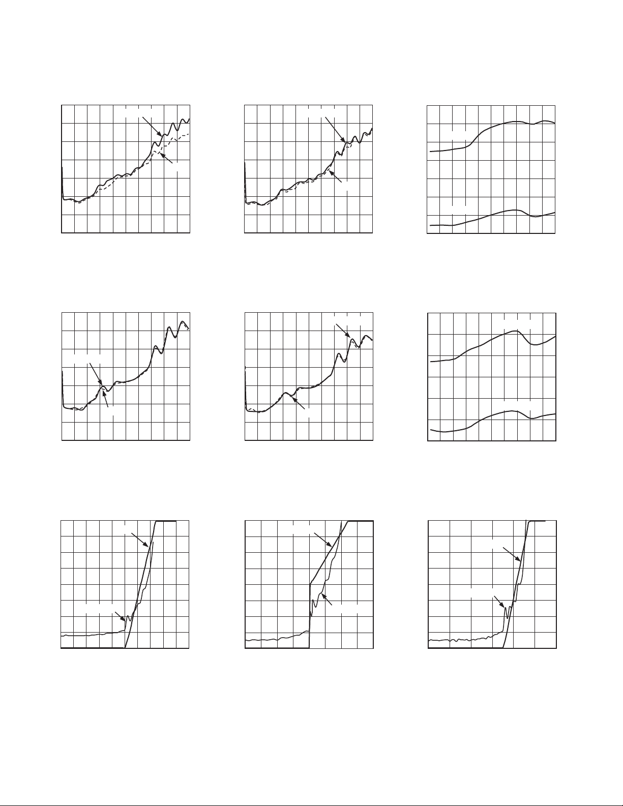
TPC 10a. Noise Figure vs. BW (Minimum Attenuation, f
11.5
11.0
10.5
10.0
9.5
9.0
8.5
NOISE FIGURE – dB
8.0
7.5
7.0
0
BW = 12.04kHz
(K = 0, M = 8)
VGA ATTENUATION – dB
= 13 MSPS)
CLK
BW = 27.08kHz
(K = 0, M = 3)
BW = 6.78kHz
(K = 0, M = 15)
93
126
10.0
9.5
16-BIT
DATA
9.0
8.5
NOISE FIGURE – dB
8.0
7.5
10
CHANNEL BANDWIDTH – kHz
16-BIT DATA
w/ DVGA
ENABLED
24-BIT
DATA
1000100
TPC 10b. Noise Figure vs. BW (Minimum Attenuation, f
14
13
12
11
10
NOISE FIGURE – dB
9
8
7
0
(K = 0, M = 1)
BW = 50kHz
(K = 0, M = 2)
VGA ATTENUATION – dB
CLK
BW = 75kHz
= 18 MSPS)
BW = 15kHz
(K = 0, M = 9)
93
126
10.0
9.5
16-BIT
9.0
8.5
NOISE FIGURE – dB
8.0
7.5
DATA
10
CHANNEL BANDWIDTH – kHz
TPC 10c. Noise Figure vs. BW (Minimum Attenuation, f
14
13
BW = 90.28kHz
12
(K = 1, M = 2)
11
10
NOISE FIGURE – dB
9
8
7
0
VGA ATTENUATION – dB
= 107.4 MHz,
1
16-BIT DATA
w/ DVGA
ENABLED
= 26 MSPS)
CLK
BW = 135.42kHz
(K = 1, M = 1)
BW = 27.08kHz
24-BIT
DATA
(K = 1, M = 9)
93
1000100
126
TPC 11a. Noise Figure vs. VGA
Attenuation (f
–30
–40
–50
–60
–70
–80
IMD – dBc
–90
–100
–110
–120
–130
–42 –39 –36 –33 –30 –27 –24
–45
TPC 12a. IMD vs. IFIN (f
1
Data taken with Toko FSLM series 10 µH inductors.
2
High Bias corresponds to LNA_Mixer Setting of 33 in SPI Register 0x01.
3
Low Bias corresponds to LNA_Mixer Setting of 12 in SPI Register 0x01.
= 13 MSPS)
CLK
PIN
LOW BIAS
IFIN – dBm
HIGH BIAS
= 13 MSPS)
CLK
–5
–10
–15
–20
–25
–30
–35
–40
–45
POUT – dBFS
TPC 11b. Noise Figure vs. VGA
Attenuation (f
–30
–40
–50
–60
–70
–80
IMD – dBc
–90
–100
–110
–120
–130
–42 –39 –36 –33 –30 –27 –24
–45
TPC 12b. IMD vs. IFIN (f
REV. A
CLK
PIN
LOW BIAS
IFIN – dBm
–11–
= 18 MSPS)
HIGH BIAS
= 18 MSPS)
CLK
–5
–10
–15
–20
–25
–30
–35
–40
–45
TPC 11c. Noise Figure vs. VGA
Attenuation (f
–30
–40
–50
–60
–70
–80
–90
PIN – dBFS
IMD – dBc
–100
–110
–120
–130
–42 –39 –36 –33 –30 –27 –24
–45
TPC 12c. IMD vs. IFIN (f
= 26 MSPS)
CLK
PIN
LOW BIAS
IFIN – dBm
HIGH BIAS
= 26 MSPS)
CLK
–5
–10
–15
–20
–25
–30
–35
–40
–45
PIN – dBFS
AD9874
INTERFERER LEVEL – dBm
NOISE FIGURE – dBc
16
–65
8
15
13
11
10
9
–5–15
NOISE FIGURE
AGC ATTN
14
12
–25–35–45–55
MEAN AGC ATTN VALUE
128
0
32
96
64
(VDDI = VDDF = VDDA = VDDC = VDDL = VDDD = VDDH = VDDx, VDDQ = VDDP = 5.0 V,
f
= 18 MSPS,
CLK
fIF
= 109.56 MHz,
f
LO
TA = 25C, LO = –5 dBm, LO and CLK Synthesizer Disabled, 16-Bit Data with AGC and DVGA enabled, unless otherwise noted.)
13
12
11
10
9
NOISE FIGURE – dB
8
7
6
0
50 500100 150 200 250 300 350 400 450
16-BIT w/DVGA
24-BIT
FREQUENCY – MHz
TPC 13a. Noise Figure vs. Frequency
(Minimum Attenuation, f
= 18 MSPS,
CLK
BW = 10 kHz, High Bias)
13
12
11
16-BIT w/DVGA
10
9
NOISE FIGURE – dB
8
7
24-BIT
13
12
11
10
9
NOISE FIGURE – dB
8
7
6
0
50 500100 150 200 250 300 350 400 450
16-BIT w/DVGA
24-BIT
FREQUENCY – MHz
TPC 13b. Noise Figure vs. Frequency
(Minimum Attenuation, f
= 18 MSPS,
CLK
BW = 10 kHz, Low Bias)
13
12
11
10
9
NOISE FIGURE – dB
8
7
16-BIT w/DVGA
24-BIT
4
2
HIGH BIAS
0
–2
–4
IIP3 – dBm
–6
LOW BIAS
–8
–10
0
50 500100 150 200 250 300 350 400 450
FREQUENCY – MHz
TPC 13c. Input IP3 vs. Frequency
= 18 MSPS)
(f
CLK
2
0
–2
–4
IIP3 – dBm
–6
–8
= 107.4 MHz,
1
HIGH BIAS
LOW BIAS
6
50 500100 150 200 250 300 350 400 450
0
FREQUENCY – MHz
TPC 14a. Noise Figure vs. Frequency
(Minimum Attenuation, f
BW = 24 kHz, High Bias)
20.0
18.5
17.0
15.5
14.0
12.5
NOISE FIGURE – dBc
11.0
9.5
8.0
–55
TPC 15a. Noise Figure vs. Interferer
Level (16-Bit Data, BW = 12.5 kHz,
AGCR = 1, f
1
Data taken with Toko FSLM series 10 µH inductors.
2
High Bias corresponds to LNA_Mixer Setting of 33 in SPI Register 0x01.
3
Low Bias corresponds to LNA_Mixer Setting of 12 in SPI Register 0x01.
NOISE FIGURE
INTERFERER LEVEL – dBm
AGC
INTERFERER
= fIF + 110 kHz)
= 26 MSPS,
CLK
–15–20–25–30–35–40–45–50
6
0
50 500100 150 200 250 300 350 400 450
FREQUENCY – MHz
TPC 14b. Noise Figure vs. Frequency
(Minimum Attenuation, f
= 26 MSPS,
CLK
–10
50 500100 150 200 250 300 350 400 450
0
FREQUENCY – MHz
TPC 14c. Input IP3 vs. Frequency
= 26 MSPS)
(f
CLK
BW = 24 kHz, Low Bias)
128
112
96
80
64
48
32
16
0
–5–10
16
15
14
13
12
11
NOISE FIGURE – dBc
10
MEAN AGC ATTN VALUE
9
8
–50
AGC ATTN
NOISE FIGURE
–20–25–30–35–40–45
INTERFERER LEVEL – dBm
TPC 15b. Noise Figure vs. Interferer
Level (16-Bit Data with DVGA, BW =
12.5 kHz, AGCR = 1, f
+ 110 kHz)
f
IF
INTERFERER
–12–
=
256
224
192
160
128
96
64
MEAN AGC ATTN VALUE
32
0
–10–15
TPC 15c. Noise Figure vs. Interferer
Level (24-Bit Data, BW = 12.5 kHz,
AGCR = 1, f
INTERFERER
= fIF + 110 kHz)
REV. A
 Loading...