

REV. 0
Information furnished by Analog Devices is believed to be accurate and
reliable. However, no responsibility is assumed by Analog Devices for its
use, nor for any infringements of patents or other rights of third parties
which may result from its use. No license is granted by implication or
otherwise under any patent or patent rights of Analog Devices.
a
AD9873
One Technology Way, P.O. Box 9106, Norwood, MA 02062-9106, U.S.A.
Tel: 781/329-4700 World Wide Web Site: http://www.analog.com
Fax: 781/326-8703 © Analog Devices, Inc., 2000
Analog Front End Converter for
Set-Top Box, Cable Modem
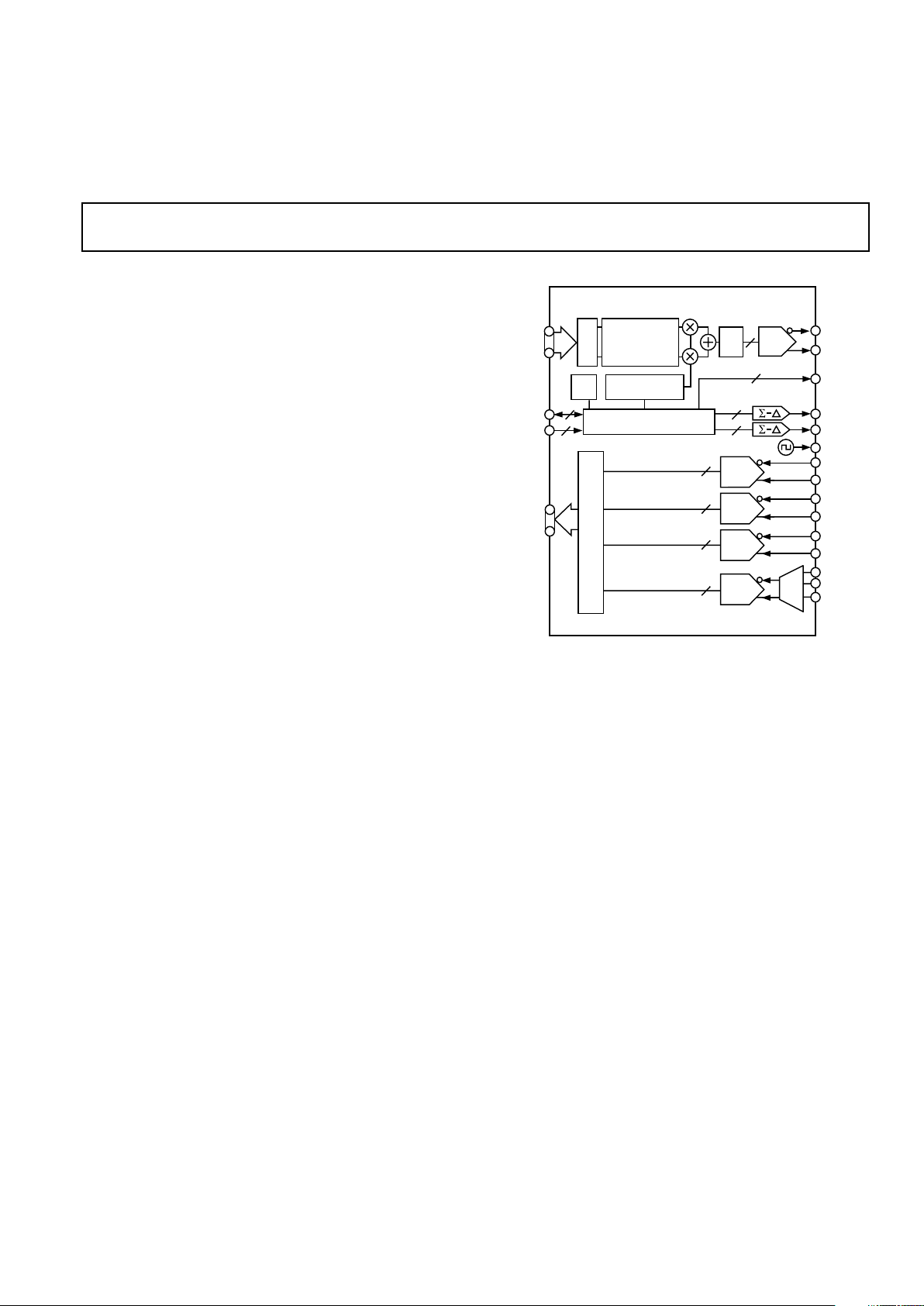
FUNCTIONAL BLOCK DIAGRAM
DAC
INV
SINC
12
Tx
INTERPOLATOR
FILTER
PLL DDS
SIN
COS
3
12
12
4
2
MUX
8
8
10
12
Tx IQ
Tx SYNC
SERIAL ITF
PROFILE
Rx SYNC
Rx IQ
Rx IF
AD9873
CA
SDELTA0
SDELTA1
REF CLK
I
IN
Q
IN
IF10
IF12
VIDEO
Tx
CONTROL FUNCTIONS
Rx
ADC
ADC
ADC
ADC
FEATURES
Low-Cost 3.3 V CMOS Analog Front End Converter for
MCNS-DOCSIS, DVB, DAVIC-Compliant
Set-Top Box, Cable Modem Applications
232 MHz Quadrature Digital Upconverter
DC to 65 MHz Output Bandwidth
12-Bit Direct IF D/A Converter (TxDAC+
®
)
Programmable Reference Clock Multiplier (PLL)
Direct Digital Synthesis
Interpolator
SIN(x)/x Compensation Filter
Four Programmable, Pin-Selectable Modulator Profiles
Single-Tone Mode for Frequency Synthesis Applications
12-Bit, 33 MSPS Sampling Direct IF A/D Converter with
Auxiliary Automatic Clamp Video Input Multiplexer
10-Bit, 33 MSPS Sampling Direct IF A/D Converter
Dual 8-Bit, 16.5 MSPS Sampling IQ A/D Converter
Two Independently Programmable Sigma-Delta
Converters
Direct Interface to AD8321/AD8323 PGA Cable Driver
Programmable Frequency Output
Power-Down Modes
APPLICATIONS
Cable and Satellite Systems
PC Multimedia
Digital Communications
Data and Video Modems
Cable Modem
Set-Top Boxes
Powerline Modem
Broadband Wireless Communication
GENERAL DESCRIPTION
The AD9873 integrates a complete 232 MHz quadrature
digital transmitter and a multichannel receiver with four highperformance analog-to-digital converters (ADC) for various
video and digital data signals. The AD9873 is designed for cable
modem set-top box applications, where cost, size, power dissipation, and dynamic performance are critical attributes. A single
external crystal is used to control all internal conversion and
data processing cycles.
The transmit section of the AD9873 includes a high-speed
direct digital synthesizer (DDS), a high-performance, high-speed
12-bit digital-to-analog converter (DAC), programmable clock
multiplier circuitry, digital filters, and other digital signal
processing functions, to form a complete quadrature digital
up-converter device.
On the receiver side, two 8-bit ADCs are optimized for IQ
demodulated “out-of band” signals. An on-chip 10-bit ADC
is typically used as a direct IF input of 256 QAM modulated
signals in cable modem applications. A second direct IF input
and an auxiliary video input with automatic programmable clamp
function are multiplexed to a high-performance 12-bit video ADC.
The chip’s programmable sigma-delta modulated outputs and
an output clock may be used to control external components
such as programmable gain amplifiers (PGA) and mixer stages.
Three pins provide a direct interface to the AD8321/AD8323
programmable gain amplifier (PGA) cable driver.
The AD9873 is available in a space-saving 100-lead MQFP package.
TxDAC+ is a registered trademark of Analog Devices, Inc.

REV. 0
AD9873
–2–
Page
FEATURES . . . . . . . . . . . . . . . . . . . . . . . . . . . . . . . . . . . . 1
GENERAL DESCRIPTION . . . . . . . . . . . . . . . . . . . . . . . . 1
SPECIFICATIONS . . . . . . . . . . . . . . . . . . . . . . . . . . . . . . 3
ABSOLUTE MAXIMUM RATINGS . . . . . . . . . . . . . . . . 7
THERMAL CHARACTERISTICS . . . . . . . . . . . . . . . . . . 7
EXPLANATION OF TEST LEVELS . . . . . . . . . . . . . . . . 7
ORDERING GUIDE . . . . . . . . . . . . . . . . . . . . . . . . . . . . . 7
DEFINITIONS OF TERMS . . . . . . . . . . . . . . . . . . . . . . . 8
PIN FUNCTION DESCRIPTIONS . . . . . . . . . . . . . . . . . 9
PIN CONFIGURATION . . . . . . . . . . . . . . . . . . . . . . . . . 10
REGISTER BIT DEFINITIONS . . . . . . . . . . . . . . . . . . . 12
TYPICAL PERFORMANCE CHARACTERISTICS . . . 14
Typical Power Consumption Characteristics . . . . . . . . . 14
Dual Sideband Transmit Spectrum . . . . . . . . . . . . . . . . 14
Single Sideband Transmit Spectrum . . . . . . . . . . . . . . . 15
Typical QAM Transmit Performance Characteristics . . 16
Typical ADC Performance Characteristics . . . . . . . . . . . 18
THEORY OF OPERATION . . . . . . . . . . . . . . . . . . . . . . 20
Transmit Section . . . . . . . . . . . . . . . . . . . . . . . . . . . . . . 21
OSC IN Clock Multiplier . . . . . . . . . . . . . . . . . . . . . . . . 21
Receive Section . . . . . . . . . . . . . . . . . . . . . . . . . . . . . . . 21
CLOCK AND OSCILLATOR CIRCUITRY . . . . . . . . . . 22
PROGRAMMABLE CLOCK OUTPUT REF CLK . . . . 23
SIGMA-DELTA OUTPUTS . . . . . . . . . . . . . . . . . . . . . . 23
SERIAL INTERFACE FOR REGISTER CONTROL . . . 23
General Operation of the Serial Interface . . . . . . . . . . . . 23
Instruction Byte . . . . . . . . . . . . . . . . . . . . . . . . . . . . . . . 23
Serial Interface Port Pin Description . . . . . . . . . . . . . . . 24
MSB/LSB Transfers . . . . . . . . . . . . . . . . . . . . . . . . . . . . 24
Notes on Serial Port Operation . . . . . . . . . . . . . . . . . . . 24
Page
TRANSMIT PATH (Tx) . . . . . . . . . . . . . . . . . . . . . . . . . 24
Transmit Timing . . . . . . . . . . . . . . . . . . . . . . . . . . . . . . 24
Data Assembler . . . . . . . . . . . . . . . . . . . . . . . . . . . . . . . 24
Half-Band Filters (HBFs) . . . . . . . . . . . . . . . . . . . . . . . 25
Cascaded Integrator—COMB (CIC) Filter . . . . . . . . . . 25
Combined Filter Response . . . . . . . . . . . . . . . . . . . . . . . 25
Inverse SINC Filter (ISF) . . . . . . . . . . . . . . . . . . . . . . . 27
Tx Signal Level Considerations . . . . . . . . . . . . . . . . . . . 28
Tx Throughput and Latency . . . . . . . . . . . . . . . . . . . . . 28
D/A Converter . . . . . . . . . . . . . . . . . . . . . . . . . . . . . . . . 28
PROGRAMMING/WRITING THE AD8321/AD8323
CABLE DRIVER AMPLIFIER GAIN CONTROL . . . 29
RECEIVE PATH (Rx) . . . . . . . . . . . . . . . . . . . . . . . . . . . 30
ADC Theory of Operation . . . . . . . . . . . . . . . . . . . . . . . 30
Receive Timing . . . . . . . . . . . . . . . . . . . . . . . . . . . . . . . 30
Driving the Analog Inputs . . . . . . . . . . . . . . . . . . . . . . . 30
Op Amp Selection Guide . . . . . . . . . . . . . . . . . . . . . . . . 31
ADC Differential Inputs . . . . . . . . . . . . . . . . . . . . . . . . 31
ADC Voltage References . . . . . . . . . . . . . . . . . . . . . . . . 31
Video Input . . . . . . . . . . . . . . . . . . . . . . . . . . . . . . . . . . 31
POWER AND GROUNDING CONSIDERATIONS . . . 32
EVALUATION BOARD . . . . . . . . . . . . . . . . . . . . . . . . . 33
Hardware . . . . . . . . . . . . . . . . . . . . . . . . . . . . . . . . . . . . 33
Software . . . . . . . . . . . . . . . . . . . . . . . . . . . . . . . . . . . . . 33
OUTLINE DIMENSIONS . . . . . . . . . . . . . . . . . . . . . . . . 39
TABLE OF CONTENTS

REV. 0
–3–
AD9873
(VAS = 3.3 V ⴞ 5%, VDS = 3.3 V ⴞ 10%, f
OSCIN
= 27 MHz, f
SYSCLK
= 216 MHz, f
MCLK
= 54 MHz
(M = 8, N = 4), ADC Sample Rate derived from PLL f
MCLK
, R
SET
= 10 k⍀, 75 ⍀ DAC Load)
Test
Parameter Temp Level Min Typ Max Unit
SYSTEM CLOCK, DAC SAMPLING f
SYSCLK
Frequency Range Full III 232 MHz
OSC IN and XTAL CHARACTERISTICS
Frequency Range Full III 3 33 MHz
Duty Cycle 25C III 35 50 65 %
Input Capacitance 25CIV 3 pF
Input Resistance 25C IV 100 MΩ
MCLK OUT JITTER (f
MCLK
Derived from PLL) 25C IV 6 ps rms
TxDAC CHARACTERISTICS
1
Resolution N/A N/A 12 Bits
Full-Scale Output Current Full III 2 4 20 mA
Gain Error (Using Internal Reference) 25C I –3 0.14 +3 % FS
Output Offset 25C I –1 +1 % FS
Reference Voltage (REFIO Level) 25°C I 1.18 1.23 1.28 V
Differential Nonlinearity (DNL) 25CIV ±2.5 LSB
Integral Nonlinearity (INL) 25CIV ±8 LSB
Output Capacitance 25CIV 5 pF
Phase Noise @ 1 kHz Offset, 42 MHz 25C IV –113 dBc/Hz
Output Voltage Compliance Range Full III –0.5 +1.5 V
Wideband SFDR
5 MHz Analog Out, I
OUT
= 4 mA 25C IV 59 dBc
65 MHz Analog Out, I
OUT
= 4 mA 25C IV 54 dBc
Narrowband SFDR (100 kHz Window)
65 MHz Analog Out, I
OUT
= 4 mA 25C IV 79 dBc
Tx MODULATOR CHARACTERISTICS
I/Q Offset Full III 50 55 dB
Pass Band Amplitude Ripple (f < f
IQCLK
/8) Full III 0.1 dB
Pass Band Amplitude Ripple (f < f
IQCLK
/4) Full III 0.5 dB
Stop Band Response (f > f
IQCLK
× 3/4) Full III –63 dB
8-BIT ADC CHARACTERISTICS
Resolution N/A N/A 8 Bits
Conversion Rate Full III 16.5 MHz
Pipeline Delay N/A N/A 3.5 ADC Cycles
DC Accuracy
Differential Nonlinearity 25CIV 0.5 LSB
Integral Nonlinearity 25CIV 0.5 LSB
Offset Error for Each 8-Bit ADC 25CIV 0.75 % FSR
Gain Error for Each 8-Bit ADC 25CIV 4 % FSR
Offset Matching Between 8-Bit ADCs Full IV 3 LSB
Gain Matching Between 8-Bit ADCs Full IV 4.5 LSB
Analog Input
Input Voltage Range Full IV 1 V p-p
Input Capacitance 25C IV 1.4 pF
Differential Input Resistance 25CIV 4 kΩ
Aperture Delay 25C IV 2.0 ns
Aperture Uncertainty (Jitter) 25C IV 1.2 ps rms
Input Bandwidth (–3 dB) 25C IV 90 MHz
Input Referred Noise 25C IV 600 µV
Reference Voltage Error
REFT8–REFB8 (0.5 V) 25CI ±4 ±92 mV
Dynamic Performance (A
IN
= –0.5 dB FS, f = 5 MHz)
Signal-to-Noise and Distortion Ratio (SINAD) Full II 43.5 48 dB
SPECIFICATIONS

REV. 0
–4–
AD9873–SPECIFICATIONS
Test
Parameter Temp Level Min Typ Max Unit
8-BIT ADC CHARACTERISTICS (Continued)
Dynamic Performance (A
IN
= –0.5 dB FS, f = 5 MHz)
Effective Number of Bits (ENOB) Full II 6.9 7.68 Bits
Effective Number of Bits (ENOB)
2
Full IV 7.68 Bits
Signal-to-Noise Ratio (SNR) Full II 43.5 48 dB
Total Harmonic Distortion (THD) Full II –66 –57 dB
Spurious Free Dynamic Range (SFDR) Full II 58 64 dB
Differential Phase 25C IV <0.1 Degree
Differential Gain 25C IV 1 LSB
10-BIT ADC CHARACTERISTICS
Resolution N/A N/A 10 Bits
Conversion Rate Full III 33 MHz
Pipeline Delay N/A N/A 5.5 ADC Cycles
DC Accuracy
Differential Nonlinearity 25CIV 0.75 LSB
Integral Nonlinearity 25CIV 0.5 LSB
Offset Error 25CIV 0.5 % FSR
Gain Error 25CIV 3 % FSR
Analog Input
Input Voltage Range Full IV 2 V p-p
Input Capacitance 25C IV 1.4 pF
Differential Input Resistance 25CIV 4 kΩ
Aperture Delay 25C IV 2.0 ns
Aperture Uncertainty (Jitter) 25C IV 1.2 ps rms
Input Bandwidth (–3 dB) 25C IV 95 MHz
Input Referred Noise 25C IV 350 µV
Reference Voltage
REFT10–REFB10 (1 V) 25CI ±6 ±200 mV
Dynamic Performance (A
IN
= –0.5 dB FS, f = 5 MHz)
Signal-to-Noise and Distortion Ratio (SINAD) Full II 57.9 60.1 dB
Effective Number of Bits (ENOB) Full II 9.3 9.7 Bits
Effective Number of Bits (ENOB)
3
Full IV 9.8 Bits
Signal-to-Noise Ratio (SNR) Full II 58.2 60.1 dB
Total Harmonic Distortion (THD) Full II –75.8 –63.9 dB
Spurious Free Dynamic Range (SFDR) Full II 65.7 80 dB
Differential Phase 25C IV <0.1 Degree
Differential Gain 25C IV <1 LSB
12-BIT ADC CHARACTERISTICS
Resolution N/A N/A 12 Bits
Conversion Rate Full III 33 MHz
Pipeline Delay N/A N/A 5.5 ADC Cycles
DC Accuracy
Differential Nonlinearity 25CIV 0.75 LSB
Integral Nonlinearity 25CIV 1.5 LSB
Offset Error 25CIV 1 % FSR
Gain Error 25CIV 2 % FSR
Analog Input
Input Voltage Range Full IV 2 V p-p
Input Capacitance 25C IV 1.4 pF
Differential Input Resistance 25CIV 4 kΩ
Aperture Delay 25C IV 2.0 ns
Aperture Uncertainty (Jitter) 25C IV 1.2 ps rms
Input Bandwidth (–3 dB) 25C IV 85 MHz
Input Referred Noise 25CIV 75 µV
Reference Voltage
REFT12–REFB12 (1 V) 25CI ±6 ±200 mV

REV. 0
–5–
AD9873
Test
Parameter Temp Level Min Typ Max Unit
12-BIT ADC CHARACTERISTICS (Continued)
Dynamic Performance (A
IN
= –0.5 dB FS, f = 5 MHz)
Signal-to-Noise and Distortion Ratio (SINAD) Full III 62.3 65 dB
Signal-to-Noise and Distortion Ratio (SINAD)
3
Full IV 67.4 dB
Effective Number of Bits (ENOB) Full III 10.0 10.5 Bits
Effective Number of Bits (ENOB)
3
Full IV 10.8 Bits
Signal-to-Noise Ratio (SNR) Full III 63.3 65.3 dB
Signal-to-Noise Ratio (SNR)
3
Full IV 67.4 dB
Total Harmonic Distortion (THD) Full III –77.6 –65.4 dB
Total Harmonic Distortion (THD)
3
Full IV –77.6 dB
Spurious Free Dynamic Range (SFDR) Full III 65.7 80 dB
Spurious Free Dynamic Range (SFDR)
3
Full IV 80 dB
Differential Phase 25C IV <0.1 Degree
Differential Gain 25C IV <1 LSB
VIDEO CLAMP INPUT
Input Voltage Range Full IV 2 V
Clamp Current Positive 25C IV 1.3 mA
Clamp Droop Current 25CIV 2 A
Clamp Level Offset Programming Range 25C III 256 512 2032 LSB
Clamp Level Resolution 25C IV 16 LSB
Carrier Rejection Filter Bandwidth (–3 dB) 25C IV 0.6 MHz
Dynamic Performance (A
IN
= –0.5 dB FS, f = 5 MHz)
Signal-to-Noise and Distortion Ratio (SINAD) Full IV 52 dB
Effective Number of Bits (ENOB) Full IV 8.34 Bits
Signal-to-Noise Ratio (SNR) Full IV 61.0 dB
Total Harmonic Distortion (THD) Full IV –53.0 dB
Spurious Free Dynamic Range (SFDR) Full IV 55.0 dB
Differential Phase 25°C IV <0.1 Degree
Differential Gain 25°C IV <8 LSB
CHANNEL-TO-CHANNEL ISOLATION
Tx DAC-to-ADC Isolation
(5 MHz Analog Output)
Isolation Between Tx and 8-Bit ADCs 25C IV >80 dB
Isolation Between Tx and 10-Bit ADC 25C IV >85 dB
Isolation Between Tx and 12-Bit ADC 25C IV >90 dB
ADC-to-ADC Isolation
(A
IN
= –0.5 dB FS, f = 5 MHz)
Isolation Between IF12 and Video 25C III 70 >70 dB
Isolation Between IF10 and IF12 25C IV >80 dB
Isolation Between Q in and IF10 25C IV >80 dB
Isolation Between Q in and I Inputs 25C IV >70 dB
TIMING CHARACTERISTICS
(20 pF Load)
Wake-Up Time N/A N/A 200 t
MCLK
Cycles
Minimum RESET Pulsewidth Low (t
RL
) N/A N/A 5 t
MCLK
Cycles
Digital Output Rise/Fall Time 25C III 2.8 4 ns
Tx/Rx Interface
MCLK Frequency (f
MCLK
)25C III 66 MHz
TxSYNC/TxIQ Set Up Time (t
SU
)25C III 3 ns
TxSYNC/TxIQ Hold Time (t
HD
)25C III 3 ns
RxSYNC/RxIQ/IF to Valid Time (t
TV
)25C III 5.2 ns
RxSYNC/RxIQ/IF Hold Time (t
HT
)25C III 0.2 ns
Serial Control Bus
SCLK Frequency (f
SCLK
) Full III 15 MHz
Clock Pulsewidth High (t
PWH
) Full III 30 ns
Clock Pulsewidth Low (t
PWL
) Full III 30 ns
Clock Rise/Fall Time Full III 1 ms
Data/Chip-Select Setup Time (t
DS
) Full III 25 ns
Data Hold Time (t
DH
) Full III 0 ns
Data Valid Time (tDV) Full III 30 ns

REV. 0
–6–
AD9873–SPECIFICATIONS
Test
Parameter Temp Level Min Typ Max Unit
CMOS LOGIC INPUTS
Logic “1” Voltage 25C III 2.0 V
Logic “0” Voltage 25C III 0.8 V
Logic “1” Current 25C III 12 A
Logic “0” Current 25C III 12 A
Input Capacitance 25CIV 3 pF
CMOS LOGIC OUTPUTS (1 mA Load)
Logic “1” Voltage 25C III 2.4 V
Logic “0” Voltage 25C III 0.4 V
POWER SUPPLY
Analog Supply Current I
AS
25C II 91 115 mA
Digital Supply Current I
DS
Full Operating Conditions4 (Register 02h = 00h) 25C IV 250 mA
Zero Input Tx
4
(Register 02h = 00h) 25C II 175 205 mA
25% Tx Burst Duty Cycle
4
(Register 02h = 00h) 25C IV 210 mA
Power-Down Digital Tx (Register 02h = 20h) 25°CII 42 55 mA
Power Supply Rejection (Differential Signal)
Tx DAC 25C IV <0.25 % FS
8-Bit ADC 25C IV <0.004 % FS
10-Bit ADC 25C IV <0.002 % FS
12-Bit ADC 25C IV <0.0004 % FS
NOTES
1
Single tone generated by applying a 1.6875 MHz sine signal to the Q Channel and the 90 degree phase shifted (cosine) signal to the I Channel.
2
Sampling directly with f
OSCCIN
/2. No degradation due to Clock Multiplier PLL. ADC Clock Select Register 08h, Bits 5 and 7 set to “1.”
3
Sampling directly with f
OSCCIN
. No degradation due to Clock Multiplier PLL. ADC Clock Select Register 08h, Bits 5 and 7 set to “1.”
4
See performance graph TPC 2 for power saving in burst mode operation.

REV. 0
AD9873
–7–
ABSOLUTE MAXIMUM RATINGS*
Power Supply (VAS, VDS) . . . . . . . . . . . . . . . . . . . . . . 3.9 V
Digital Output Current . . . . . . . . . . . . . . . . . . . . . . . . . 5 mA
Digital Inputs . . . . . . . . . . . . . . . –0.3 V to DRVDD + 0.3 V
Analog Inputs . . . . . . . . . . . . . –0.3 V to AVDD (IQ) +0.3 V
Operating Temperature . . . . . . . . . . . . . . . . . . . . 0C to 70C
Maximum Junction Temperature . . . . . . . . . . . . . . . . 150C
Storage Temperature . . . . . . . . . . . . . . . . . . –65C to +150C
Lead Temperature (Soldering 10 sec) . . . . . . . . . . . . . 300C
*Absolute maximum ratings are limiting values, to be applied individually, and
beyond which the serviceability of the circuit may be impaired. Functional
operability under any of these conditions is not necessarily implied. Exposure of
absolute maximum rating conditions for extended periods of time may affect
device reliability.
EXPLANATION OF TEST LEVELS
I – 100% production tested.
II – Devices are 100% production tested at 25C and guaran-
teed by design and characterization testing for commercial
operating temperature range (0C to 70C).
III – Parameter is guaranteed by design and/or characteriz-
ation testing.
IV – Parameter is a typical value only.
N/A – Test level definition is not applicable.
THERMAL CHARACTERISTICS
Thermal Resistance
100-Lead MQFP
JA
= 40.5C/W
CAUTION
ESD (electrostatic discharge) sensitive device. Electrostatic charges as high as 4000 V readily
accumulate on the human body and test equipment and can discharge without detection. Although
the AD9873 features proprietary ESD protection circuitry, permanent damage may occur on
devices subjected to high-energy electrostatic discharges. Therefore, proper ESD precautions are
recommended to avoid performance degradation or loss of functionality.
WARNING!
ESD SENSITIVE DEVICE
ORDERING GUIDE
Temperature Package Package
Model Range Description Option
AD9873JS 0C to 70C Metric Quad Flatpack (MQFP) S-100C
AD9873-EB Evaluation Board

REV. 0
AD9873
–8–
DEFINITIONS OF TERMS
DIFFERENTIAL NONLINEARITY ERROR (DNL, NO
MISSING CODES)
An ideal converter exhibits code transitions that are exactly 1 LSB
apart. DNL is the deviation from this ideal value. Guaranteed
no missing codes to 10-bit resolution indicates that all 1024 codes
respectively, must be present over all operating ranges.
INTEGRAL NONLINEARITY ERROR (INL)
Linearity error refers to the deviation of each individual code
from a line drawn from “negative full scale” through “positive
full scale.” The point used as “negative full scale” occurs 1/2 LSB
before the first code transition. “Positive full scale” is defined as
a level 1 1/2 LSB beyond the last code transition. The deviation
is measured from the middle of each particular code to the true
straight line.
PHASE NOISE
Single-sideband phase noise power density is specified relative to
the carrier (dBc/Hz) at a given frequency offset (1 kHz) from
the carrier. Phase noise can be measured directly in single tone
transmit mode with a spectrum analyzer that supports noise
marker measurements. It detects the relative power between the
carrier and the offset (1 kHz) sideband noise and takes the resolution bandwidth (rbw) into account by subtracting 10 log (rbw).
It also adds a correction factor that compensates for the implementation of the resolution bandwidth, log display and detector
characteristic.
OUTPUT COMPLIANCE RANGE
The range of allowable voltage at the output of a current-output
DAC. Operation beyond the maximum compliance limits may
cause either output stage saturation, resulting in nonlinear performance or breakdown.
SPURIOUS-FREE DYNAMIC RANGE (SFDR)
The difference, in dB, between the rms amplitude of the DACs
output signal (or ADC’s input signal) and the peak spurious
signal over the specified bandwidth (Nyquist bandwidth unless
otherwise noted).
PIPELINE DELAY (LATENCY)
The number of clock cycles between conversion initiation and the
associated output data being made available.
OFFSET ERROR
First transition should occur for an analog value 1/2 LSB above
negative full scale. Offset error is defined as the deviation of the
actual transition from that point.
GAIN ERROR
The first code transition should occur at an analog value 1/2 LSB
above negative full scale. The last transition should occur for an
analog value 1 1/2 LSB below the nominal full scale. Gain error
is the deviation of the actual difference between first and last
code transitions and the ideal difference between first and last
code transitions.
APERTURE DELAY
Aperture delay is a measure of the Sample-and-Hold Amplifier
(SHA) performance and specifies the time delay between the
rising edge of the sampling clock input to when the input signal
is held for conversion.
APERTURE UNCERTAINTY (JITTER)
Aperture jitter is the variation in aperture delay for successive
samples and is manifested as noise on the input to the ADC.
SIGNAL-TO-NOISE + DISTORTION (SINAD) RATIO
SINAD is the ratio of the rms value of the measured input signal
to the rms sum of all other spectral components below the Nyquist
frequency, including harmonics but excluding dc. The value for
SINAD is expressed in decibels.
EFFECTIVE NUMBER OF BITS (ENOB)
For a sine wave, SINAD can be expressed in terms of the number
of bits. Using the following formula,
N = (SINAD – 1.76) dB/6.02
it is possible to obtain a measure of performance expressed as N,
the effective number of bits.
SIGNAL-TO-NOISE RATIO (SNR)
SNR is the ratio of the rms value of the measured input signal to
the rms sum of all other spectral components below the Nyquist
frequency, excluding harmonics and dc. The value for SNR is
expressed in decibels.
TOTAL HARMONIC DISTORTION (THD)
THD is the ratio of the rms sum of the first six harmonic components to the rms value of the measured input signal and is
expressed as a percentage or in decibels.
POWER SUPPLY REJECTION
Power supply rejection specifies the converters maximum full-scale
change when the supplies are varied from nominal to minimum
and maximum specified voltages.
CHANNEL-TO-CHANNEL ISOLATION (CROSSTALK)
In an ideal multichannel system, the signal in one channel will
not influence the signal level of another channel. The channelto-channel isolation specification is a measure of the change that
occurs to a grounded channel as a full-scale signal is applied to
another channel.

REV. 0
AD9873
–9–
PIN FUNCTION DESCRIPTIONS
Pin No. Mnemonic Pin Function
1, 84, 87 AVDD Analog Supply Voltage
92, 95 10-/12-Bit ADC
2, 21, 70 DRGND Pin Driver Digital Ground
3, 22, 72 DRVDD Pin Driver Digital Supply Voltage
4–15 IF11–IF0 Multiplexed Output of IF10-
and IF12-Bit ADCs
16–19 Rx IQ 3 Multiplexed Output of I and
–Rx IQ 0 Q 8-Bit ADCs
20 Rx SYNC Demultiplexer Synchronization
Output for IF and IQ ADCs
23 MCLK Master Clock Output
Demultiplexer
24, 33, 38 DVDD Digital Supply Voltage
25, 34, DGND Digital Ground
39, 40
26 Tx SYNC Synchronization Input for
Transmitter
27–32 Tx IQ 5 Multiplexed I and Q Input
–Tx IQ 0 Data for Transmitter (Two’s
Complement)
35, 36 PROFILE[1:0] Profile Selection Inputs
37 RESET Master Reset Input, Reset applies
for all Interfaces and Registers
41 SCLK Serial Interface Input Clock
42 CS Serial Interface Chip Select
43 SDIO Serial Interface Data I/O
44 SDO Serial Interface Data Output
45 DGND Tx Digital Ground Tx Section
46 DVDD Tx Digital Supply Voltage Tx
47 PWR DOWN Transmit Power-Down
Control Input
48 REFIO DAC Bandgap requires 0.1 µF
Capacitor to Ground
49 FSADJ Full-Scale DAC Current Output
Adjust with External Resistor
50 AGND Tx Analog Ground Tx Section
51 Tx– Transmitter DAC Output–
52 Tx+ Transmitter DAC Output+
53 AVDD Tx Analog Supply Voltage Tx
54 DGND PLL PLL Digital Ground
55 DVDD PLL PLL Digital Supply Voltage
56 AVDD PLL PLL Analog Supply Voltage
57 PLL FILTER PLL Loop Filter Connection
58 AGND PLL PLL Analog Ground
59 DGND OSC Digital Ground Oscillator
60 XTAL Crystal Oscillator Inv. Output
61 OSC IN Oscillator Clock Input
62 DVDD OSC Digital Supply Oscillator
63 CA CLK Cable Amplifier Control
Clock Output
Pin No. Mnemonic Pin Function
64 CA DATA Cable Amplifier Control Data
Output
65 CA ENABLE Cable Amplifier Control Enable
Output
66 DVDD SD Supply Voltage Sigma Delta
67 SDELTA1 Sigma Delta Output Stream 1
68 SDELTA0 Sigma Delta Output Stream 0
69 DGND SD Ground Sigma Delta
71 REF CLK Programmable Reference Clock
Output Derived from MCLK
73 AVDD IQ Analog Supply 8-Bit ADCs
74, 77, 80 AGND IQ Analog Ground 8-Bit ADCs
75 REFB8 Bottom Reference Decoupling
IQ 8-Bit ADC’s Reference
76 REFT8 Top Reference Decoupling
IQ 8-Bit ADC’s Reference
78 I IN– Inverting I Analog Input
79 I IN+ Noninverting I Analog Input
81 Q IN– Inverting Q Analog Input
82 Q IN+ Noninverting Q Analog Input
83, 88, 91, AGND Analog Ground 10-/12-Bit ADC
96, 99
85 REFB10 Bottom Reference Decoupling
IF 10-Bit ADC’s Reference
86 REFT10 Top Reference Decoupling
IF 10-Bit ADC’s Reference
89 IF10– Noninverting IF10 Analog Input
90 IF10+ Inverting IF10 Analog Input
93 REFB12 Bottom Reference Decoupling
IF 12-Bit ADC’s Reference
94 REFT12 Top Reference Decoupling
IF 12-Bit ADC’s Reference
97 IF12– Inverting IF12 Analog Input
98 IF12+ Noninverting IF12 Analog Input
100 VIDEO IN Single-Ended Video Input

REV. 0
AD9873
–10–
PIN CONFIGURATION
5
4
3
2
7
6
9
8
1
11
10
16
15
14
13
18
17
20
19
22
21
12
24
23
26
25
28
27
30
29
32
33
34
35
36
38
39
40
41
42
43
44
45
46
47
48
49
50
31
37
76
77
78
79
74
75
72
73
70
71
80
65
66
67
68
63
64
61
62
59
60
69
57
58
55
56
53
54
51
52
100
99989796959493929190898887868584838281
PIN 1
IDENTIFIER
TOP VIEW
(Pins Down)
VIDEO IN
AGND
IF12+
IF12–
AGND
AVDD
REFT12
REFB12
AVDD
AGND
IF10+
IF10–
AGND
AVDD
REFT10
REFB10
AVDD
AGND
Q IN+
Q IN–
TxIQ(1)
TxIQ(0)
DVDD
DGND
PROFILE(1)
PROFILE(0)
RESET
DVDD
DGND
DGND
SCLK
CS
SDIO
SDO
DGND Tx
DVDD Tx
PWR DOWN
REFIO
FSADJ
AGND Tx
AGND IQ
I IN+
I IN–
AGND IQ
REFT8
REFB8
AGND IQ
AVDD IQ
DRVDD
REF CLK
DRGND
DGND SD
SDELTA 0
SDELTA 1
DVDD SD
CA ENABLE
CA DATA
CA CLK
DVDD OSC
OSC IN
XTAL
DGND OSC
AGND PLL
PLL FILTER
AVDD PLL
DVDD PLL
DGND PLL
AVDD Tx
Tx+
Tx–
DRGND
DRVDD
(MSB) IF(11)
IF(10)
IF(9)
IF(8)
IF(7)
IF(6)
IF(5)
IF(4)
IF(3)
IF(2)
IF(1)
IF(0)
(MSB) RxIQ(3)
RxIQ(2)
RxIQ(1)
RxIQ(0)
RxSYNC
DRGND
DRVDD
MLCK
DVDD
DGND
TxSYNC
(MSB) TxIQ(5)
TxIQ(4)
TxIQ(3)
TxIQ(2)
AD9873
AVDD
REV. 0
AD9873
–11–
Table I. Register Map
Address Default
(Hex) Bit 7 Bit 6 Bit 5 Bit 4 Bit 3 Bit 2 Bit 1 Bit 0 (Hex) Type
00 SDIO LSB/MSB RESET OSC IN OSC IN OSC IN OSC IN OSC IN 10 rw
Bidirectional First Multiplier Multiplier Multiplier Multiplier Multiplier
M <4> M <3> M <2> M <1> M <0>
01 PLL OSC IN MCLK MCLK MCLK MCLK MCLK MCLK 09 rw
Lock Divider Divider Divider Divider Divider Divider Divider
Detect N = 3 (4) R <5> R <4> R <3> R <2> R <1> R <0>
02 Power-Down Power-Down Power-Down Power-Down Power-Down Power-Down Power-Down Power-Down 00 rw
PLL DAC Tx Digital Tx 12-Bit ADC Reference 10-Bit ADC Reference 8-Bit ADC
12-Bit ADC 10-Bit ADC
03 Sigma-Delta Output 0 Control Word <3:0> LSB 000000rw
04 Sigma-Delta Output 0 Control Word <11:4> MSB 00 rw
05 Sigma-Delta Output 1 Control Word <3:0> LSB 000000rw
06 Sigma-Delta Output 1 Control Word <11:4> MSB 00 rw
07 Video Input Clamp Level Control for Video Input <6:0> 20 rw ADC
Enable
08 ADC Clock 0 ADC Clock 0 0 0 Test Test 00 rw ADC
Select Select 12-Bit ADC 10-Bit ADC
090 0 00000000rw
0A0 0 00000000rw
0B0 0 0 0000000rw
0C 0 0 0 0 Version <3:0> 0X r
0D0 0 00000000r
0E0 0 0 0000000r
0F 0 0 Profile Profile 0 Bypass Spectral Single-Tone 00 rw Tx
Select <1> Select <0> Inv. Sinc Inversion Tx Tx Mode
Tx Filter
10 Tx Frequency Turning Word Profile 0 <7:0> 00 rw Tx
11 Tx Frequency Turning Word Profile 0 <15:8> 00 rw Tx
12 Tx Frequency Turning Word Profile 0 <23:16> 00 rw Tx
13 Cable Driver Amplifier Gain Control Profile 0 <7:0> 00 rw Tx
14 Tx Frequency Turning Word Profile 1 <7:0> 00 rw Tx
15 Tx Frequency Turning Word Profile 1 <15:8> 00 rw Tx
16 Tx Frequency Turning Word Profile 1 <23:16> 00 rw Tx
17 Cable Driver Amplifier Gain Control Profile 1 <7:0> 00 rw Tx
18 Tx Frequency Turning Word Profile 2 <7:0> 00 rw Tx
19 Tx Frequency Turning Word Profile 2 <15:8> 00 rw Tx
1A Tx Frequency Turning Word Profile 2 <23:16> 00 rw Tx
1B Cable Driver Amplifier Gain Control Profile 2 <7:0> 00 rw Tx
1C Tx Frequency Turning Word Profile 3 <7:0> 00 rw Tx
1D Tx Frequency Turning Word Profile 3 <15:8> 00 rw Tx
1E Tx Frequency Turning Word Profile 3 <23:16> 00 rw Tx
1F Cable Driver Amplifier Gain Control Profile 3 <7:0> 00 rw Tx
“0” register bits should not be programmed with 1.

REV. 0
AD9873
–12–
REGISTER BIT DEFINITIONS
00h, Bits 0–4: OSC IN Multiplier–Register Address
This register field is used to program the on-chip multiplier (PLL)
that generates the chip’s high-frequency system clock, f
SYSCLK
.
For example, to multiply the external crystal clock f
OSCIN
by 19
decimal, program register address 00h, Bits 5–1 as 13h. Default
value is M = 16 = 10h. Valid entries range from M = 1 to 31.
M = 1 (no PLL) requires a very stable, high-frequency clock at
OSC IN. A changed f
SYSCLK
frequency is stable (PLL locked)
after a maximum of 200 f
MCLK
cycles (= Wake-Up Time).
00h, Bit 5: RESET
Writing a one to this bit resets the registers to their default values and restarts the chip. The RESET bit always reads back
0. Register address 00h bits are not cleared by this software reset.
However, a low level at the RESET pin would force all registers,
including all bits in address 00h, to their default state.
00h, Bit 6: LSB/MSB First
Active high indicates SPI serial port access of instruction byte
and data registers is least significant bit (LSB) first. Default low
indicates most significant bit (MSB) first format.
00h, Bit 7: SDIO Bidirectional
Default low indicates SPI serial port uses dedicated input/output
lines (SDIO and SDO pin). High configures serial port as single
line I/O (SDIO pin is used bidirectional).
01h, Bits 0–5: MCLK Divider
This register is used to divide the chip’s master clock by R, where
R is an integer between 2 and 63. The generated reference clock,
REF CLK, can be used for external frequency-controlled
devices. Default value is R = 9.
01h, Bit 6: OSC IN Divider
The OSC IN multiplier output clock can be divided by 4 or 3 to
generate the chip’s master clock. Active high indicates a divide
ratio of N = 3. Default low configures a divide ratio of N = 4.
01h, Bit 7: PLL Lock Detect
If this bit is set to 1, REF CLK pin is disabled from the normal usage. In this mode REF CLK high signals that the internal
phase lock loop (PLL) is in lock with CLK IN.
02h Bits 0–7: Power-Down
Sections of the chip that are not used can be put in a power saving
mode when the corresponding bits are set to 1. This register has
a default value of 00h with all sections active.
Bit 0: Power-Down 8-bit ADC powers down the 8-bit ADC
and stops RxSYNC framing signal.
Bit 1: Power-Down 10-bit ADC reference powers down the
internal 10-bit ADC reference.
Bit 2: Power-Down 10-bit ADC powers down the 10-bit ADC.
Bit 3: Power-Down 12-bit ADC reference powers down the
internal 12-bit ADC reference.
Bit 4: Power-Down 12-bit ADC powers down the 12-bit ADC.
Bit 5: Power-Down Tx powers down the transmit section of
the chip.
Bit 6: Power-Down DAC Tx powers down the DAC.
Bit 7: Power-Down PLL powers down the CLK IN Multiplier.
03h to 06h: Sigma-Delta Output Control Words
The Sigma-Delta Output Control Words –0 and –1 are 12 bits
wide and split in MSB bits <11:4> and LSB bits <3:0>. Changes
to the sigma-delta outputs take effect immediately for every MSB
or LSB register write. Sigma-delta output control words have a
default value of 0. The smaller the programmed values in these
registers, the lower are the integrated (low-pass filtered) sigma
delta output levels (straight binary format).
07h, Bits 0–6: Clamp Level Control for Video Input
A 7-bit clamp level offset can be set for the internal automatic
clamp level control loop of the Video Input.
Clamp level offset = Clamp level control × 16.
This register defaults to 32 = 20h, which amounts to a clamp
level offset of 512 LSB = 200h. Valid clamp level control values
are 16 to 127.
07h, Bit 7: Video Input Enable
This bit controls the multiplexer to the 12-bit ADC and determines if IF12 input or Video input is used. The bit is default set
to 0 for the IF12 input.
08h, Bit 0: Test 10-Bit ADC
Active high allows nonmultiplexed 10-bit ADC data only to be
read at IF outputs. Output data changes at half MCLK clock rate.
This bit defaults to 0.
08h, Bit 1: Test 12-Bit ADC
Active high allows nonmultiplexed 12-bit ADC data only to be
read at IF outputs. Output data changes at half MCLK clock rate.
This bit defaults to 0.
08h, Bit 5 and Bit 7: ADC Clock Select
Active high indicates that the frequency at OSC IN is directly used
to sample the on chip ADCs. Default low indicates that the on
chip ADCs generate their sampling frequencies from the internally
generated master clock MCLK. Both Bit 5 and Bit 7 need to be
programmed with the same values.
0Ch, Bits 0–3: Version
This register stores the die version of the chip. It can only be read.
0Fh, Bit 0: Single-Tone Tx Mode
Active high configures the AD9873 for single-tone applications.
The AD9873 will supply a single frequency output as determined
by the frequency tuning word (FTW) selected by the active
profile. In this mode, the Tx IQ input data pins are ignored
but should be tied high or low. Default value of single-tone
Tx mode is 0 (inactive).
0Fh, Bit 1: Spectral Inversion Tx
When set to 1, inverted modulation is performed
(I cos (ωt) + Q sin (ωt)).
Default is logic zero, noninverted modulation
(I cos (ωt) – Q sin (ωt)).
0Fh, Bit 2: Bypass Inv Sinc Tx Filter
Active high, configures the AD9873 to bypass the SIN(X)/X
compensation filter. Default value is 0 (inverse sinc filter enabled).

REV. 0
AD9873
–13–
0Fh, Bit 4, Bit 5: Profile Select
The AD9873 quadrature digital upconverter is capable of storing
four preconfigured modulation modes called profiles that define
a transmit frequency tuning word and cable driver amplifier control. Profile Select bits <1:0> or PROFILE [1:0] pins program
the current register profile to be used. Profile Select bits should
always be 0 if PROFILE pins are used to switch between profiles. Using the Profile Select bits as a means of switching between
different profiles requires the PROFILE pins to be tied low.
10h–1Fh: Burst Parameter
Tx Frequency Tuning Words
The frequency tuning word (FTW) determines the DDSgenerated carrier frequency (f
C
) and is formed via a concatenation
of register addresses. Bit 7 of register address 1Ah is the most
significant bit of the profile 2-frequency tuning word. Bit 0 of
register address 18h is the least significant bit of the profile
2-frequency tuning word.
The output frequency equation is given as:
f
C
= (FTW × f
SYSCLK
)/224.
Where f
SYSCLK
= Mx f
OSCIN
and FTW < 80 00 00 h
Changes to FTW bytes immediately take effect on active profiles.
Cable Driver Gain Control
The AD9873 dedicates three output pins that directly interface to
the AD832x-family of gain programmable cable driver amplifier.
This allows direct control of the cable driver’s gain via the
AD9873. New data is automatically sent to the cable driver
amplifier whenever a new burst profile with different gain setting
becomes active or when the gain contents of an active AD8321/
AD8323 gain control register changes. Default value is 00h
(lowest gain).

REV. 0
AD9873
–14–
Typical Performance Characteristics
(VAS = 3.3 V, VDS = 3.3 V, f
OSCIN
= 27 MHz, f
SYSCLK
= 216 MHz, f
MCLK
= 54 MHz
[M = 8, N = 4], ADC Sample Rate derived directly from f
OSCIN
, R
SET
= 10 k⍀ [I
OUT
= 4 mA], 75 ⍀ DAC Load, unless otherwise noted)
f
SYSCLK
– MHz
380
240
120 140
SUPPLY CURRENT – mA
180 220
340
320
280
200
260
240
220
300
360
160 200
TPC 1. Power Consumption vs. Clock Speed, f
SYSCLK
DUTY CYCLE – %
340
300
030
SUPPLY CURRENT – mA
70 90
320
310
100
290
50 8020 40 60
SINGLE-TONE
16-QAM
330
10
TPC 2. Power Consumption vs. Transmit Burst Duty Cycle
TYPICAL POWER CONSUMPTION CHARACTERISTICS (20 MHz Single Tone, unless otherwise noted)
FREQUENCY – MHz
0
–60
06
MAGNITUDE – dB
14 18
–20
–100
–40
20
–80
10 164812
–10
–30
–50
2
–90
–70
TPC 3a. Dual Sideband Spectral Plot, fC = 5 MHz
f = 1 MHz, R
SET
=10 kΩ (I
OUT
= 4 mA), RBW = 1 kHz
FREQUENCY – MHz
0
–60
55 61
MAGNITUDE – dB
69 73
–20
–100
–40
75
–80
65 7159 63 67
–10
–30
–50
57
–90
–70
TPC 4a. Dual Sideband Spectral Plot, fC = 65 MHz
f = 1 MHz, R
SET
=10 kΩ (I
OUT
= 4 mA), RBW = 1 kHz
DUAL SIDEBAND TRANSMIT SPECTRUM (See Table IV for Dual-Tone Generation.)
FREQUENCY – MHz
0
–60
06
MAGNITUDE – dB
14 18
–20
–100
–40
20
–80
10 164812
–10
–30
–50
2
–90
–70
TPC 3b. Dual Sideband Spectral Plot, fC = 5 MHz
f = 1 MHz, R
SET
= 4 kΩ (I
OUT
= 10 mA), RBW = 1 kHz
FREQUENCY – MHz
0
–60
55 61
MAGNITUDE – dB
69 73
–20
–100
–40
75
–80
65 7159 63 67
–10
–30
–50
57
–90
–70
TPC 4b. Dual Sideband Spectral Plot, fC = 65 MHz
f = 1 MHz, R
SET
= 4 kΩ (I
OUT
= 10 mA), RBW = 1 kHz

REV. 0
AD9873
–15–
FREQUENCY – MHz
0
–60
0
MAGNITUDE – dB
80
–20
–100
–40
–80
4020 60
–10
–30
–50
–90
–70
100
TPC 5a. Single Sideband @ 65 MHz, RBW = 2 kHz
f
C
= 66 MHz, f = 1 MHz, R
SET
= 10 kΩ (I
OUT
= 4 mA)
FREQUENCY – MHz
0
–60
0
MAGNITUDE – dB
80
–20
–100
–40
–80
4020 60
–10
–30
–50
–90
–70
100
TPC 6a. Single Sideband @ 42 MHz, RBW = 2 kHz
f
C
= 43 MHz, f = 1 MHz, R
SET
= 10 kΩ (I
OUT
= 4 mA)
FREQUENCY – MHz
0
–60
0
MAGNITUDE – dB
80
–20
–100
–40
–80
4020 60
–10
–30
–50
–90
–70
100
TPC 7a. Single Sideband @ 5 MHz, RBW = 2 kHz
f
C
= 6 MHz, f = 1 MHz, R
SET
= 10 kΩ (I
OUT
= 4 mA)
FREQUENCY – MHz
0
–60
0
MAGNITUDE – dB
80
–20
–100
–40
–80
4020 60
–10
–30
–50
–90
–70
100
TPC 5b. Single Sideband @ 65 MHz, RBW = 2 kHz
f
C
= 66 MHz, f = 1 MHz, R
SET
= 4 kΩ (I
OUT
= 10 mA)
FREQUENCY – MHz
0
–60
0
MAGNITUDE – dB
80
–20
–100
–40
–80
4020 60
–10
–30
–50
–90
–70
100
TPC 6b. Single Sideband @ 42 MHz, RBW = 2 kHz
f
C
= 43 MHz, f = 1 MHz, R
SET
= 4 kΩ (I
OUT
= 10 mA)
FREQUENCY – MHz
0
–60
0
MAGNITUDE – dB
80
–20
–100
–40
–80
4020 60
–10
–30
–50
–90
–70
100
TPC 7b. Single Sideband @ 5 MHz, RBW = 2 kHz
f
C
= 6 MHz, f = 1 MHz, R
SET
= 4 kΩ (I
OUT
= 10 mA)
SINGLE SIDEBAND TRANSMIT SPECTRUM

REV. 0
AD9873
–16–
FREQUENCY OFFSET – MHz
0
–60
–2.5 –1.0
MAGNITUDE – dB
1.0 2.0
–20
–90
–40
2.5
–80
0 1.5–1.5 –0.5 0.5
–10
–30
–50
–2.0
–70
TPC 8a. Single Sideband @ 65 MHz, RBW = 500 Hz
f
C
= 66 MHz, f = 1 MHz, R
SET
= 10 kΩ (I
OUT
= 4 mA)
FREQUENCY OFFSET – kHz
0
–60
–50 –20
MAGNITUDE – dB
20 40
–20
–100
–40
50
–80
030–30 –10 10
–10
–30
–50
–40
–70
–90
TPC 9. Single Sideband @ 65 MHz, RBW = 50 Hz
f
C
= 66 MHz, f = 1 MHz, R
SET
= 10 kΩ (I
OUT
= 4 mA)
FREQUENCY – MHz
0
–60
0
MAGNITUDE – dB
35
–20
–80
–40
15525
–10
–30
–50
–70
45402010 30 50
TPC 11. 16-QAM @ 42 MHz Spectral Plot, RBW = 1 kHz
FREQUENCY OFFSET – MHz
0
–60
–2.5 –1.0
MAGNITUDE – dB
1.0 2.0
–20
–90
–40
2.5
–80
0 1.5–1.5 –0.5 0.5
–10
–30
–50
–2.0
–70
TPC 8b. Single Sideband @ 65 MHz, RBW = 500 Hz
f
C
= 66 MHz, f = 1 MHz, R
SET
= 4 kΩ (I
OUT
= 10 mA)
FREQUENCY OFFSET – kHz
0
–60
–2.5 –1.0
MAGNITUDE – dB
1.0 2.0
–20
–100
–40
2.5
–80
0 1.5–1.5 –0.5 0.5
–10
–30
–50
–2.0
–70
–90
TPC 10. Single Sideband @ 65 MHz, RBW = 10 Hz
f
C
= 66 MHz, f = 1 MHz, R
SET
= 10 kΩ (I
OUT
= 4 mA)
FREQUENCY – MHz
0
–60
0
MAGNITUDE – dB
35
–20
–80
–40
15525
–10
–30
–50
–70
45402010 30 50
TPC 12. 16-QAM @ 5 MHz Spectral Plot, RBW = 1 kHz
TYPICAL QAM TRANSMIT PERFORMANCE CHARACTERISTICS
(16-QAM, 2.56 Mbit/s SINC Filter Enabled, Square Root Raised Cosine Filter with Alpha = 0.25, R
SET
= 4 k⍀
[I
OUT
= 10 mA], f
SYSCLK
= 163.84 MHz, f
OSCIN
= 20.48 MHz [M = 8, N = 4].)

REV. 0
AD9873
–17–
TPC 13. Tx Output 16-QAM Analysis
TPC 14. Tx Output 64-QAM Analysis

REV. 0
AD9873
–18–
TYPICAL ADC PERFORMANCE CHARACTERISTICS (ADC Sample Rate derived directly from f
OSCIN
=
27 MHz [13.5 MSPS for 8-bit ADCs], Single-Tone 5 MHz Input Signal, unless otherwise noted.)
INPUT SIGNAL FREQUENCY – MHz
70
20
SNR – dB
45
60
6010 40 800
50
1005030 70 90
65
55
12-BIT ADC
10-BIT ADC
8-BIT ADC
TPC 15. SNR vs. Input Frequency
INPUT SIGNAL FREQUENCY – MHz
70
20
SINAD – dB
45
6010 40 800
50
1005030 70 90
60
55
65
12-BIT ADC
10-BIT ADC
8-BIT ADC
11.34
7.18
8.01
9.67
8.84
10.51
ENOB – Bit
TPC 16. SINAD vs. Input Frequency
INPUT SIGNAL FREQUENCY – MHz
65
6
MAGNITUDE – dB
40
14410 1822012816
55
50
60
SNR
45
SFDR
SINAD
TPC 17. Video Input Characteristics vs. Input Frequency
INPUT SIGNAL FREQUENCY – MHz
85
20
SFDR – dB
55
65
6010 40 800
60
1005030 70 90
75
80
70
10-BIT ADC
8-BIT ADC
12-BIT ADC
TPC 18. SFDR vs. Input Frequency
INPUT SIGNAL FREQUENCY – MHz
–60
20
THD – dB
–80
6010 40 800
–74
1005030 70 90
–64
–66
–62
12-BIT ADC
10-BIT ADC
8-BIT ADC
–78
–70
–72
–76
–68
TPC 19. THD vs. Input Frequency
FREQUENCY – MHz
–5
2
MAGNITUDE – dB
–125
–45
6140
–85
53
–105
–25
–65
0
TPC 20. 8-Bit ADC Single-Tone Spectral Plot Using PLL
(Input Frequency = 5 MHz, 2048 Point FFT)

REV. 0
AD9873
–19–
FREQUENCY – MHz
–5
4
MAGNITUDE – dB
–125
–45
12280
–85
106
–105
–25
–65
13.5
0
TPC 21. 12-Bit ADC Single-Tone Spectral Plot Using PLL
(Input Frequency = 10 MHz, 4096 Point FFT)
FREQUENCY – MHz
–5
4
MAGNITUDE – dB
–125
–45
12280
–85
106
–105
–25
–65
13.5
0
TPC 22. 10-Bit ADC Single-Tone Spectral Plot Using PLL
(Input Frequency = 10 MHz, 4096 Point FFT)
FREQUENCY – MHz
–5
4
MAGNITUDE – dB
–125
–45
12280
–85
106
–105
–25
–65
13.5
0
TPC 23. Video Input Single-Tone Spectral Plot Using PLL
(Input Frequency = 5 MHz, 4096 Point FFT)
FREQUENCY – MHz
–5
4
MAGNITUDE – dB
–125
–45
12280
–85
106
–105
–25
–65
13.5
0
TPC 24. 12-Bit ADC Single-Tone Spectral Plot Without PLL
(Input Frequency = 10 MHz, 4096 Point FFT)
FREQUENCY – MHz
–5
4
MAGNITUDE – dB
–125
–45
12280
–85
106
–105
–25
–65
13.5
0
TPC 25. 10-Bit ADC Single-Tone Spectral Plot Without PLL
(Input Frequency = 10 MHz, 4096 Point FFT)
FREQUENCY – MHz
–5
4
MAGNITUDE – dB
–125
–45
12280
–85
106
–105
–25
–65
13.5
0
TPC 26. Video Input Single-Tone Spectral Plot Without
PLL (Input Frequency = 5 MHz, 4096 Point FFT)

REV. 0
AD9873
–20–
THEORY OF OPERATION
To gain a general understanding of the AD9873 it is helpful
to refer to Figure 1, which displays a block diagram of the device
MUX
8
8
10
12
AD9873
I INPUT
Q INPUT
IF10 INPUT
IF12 INPUT
VIDEO INPUT
ADC
ADC
ADC
ADC
DAC
ⴜ2
(f
OSCIN
)
ⴜ2
(f
OSCIN
)
ⴜ2
MUX
MUX
REF-8
REF-10
REF-12
CLAMP LEVEL
12
CONTROL WORD 0
12
CONTROL WORD 1
OSC IN
MULTIPLIER
ⴛ M
M = 1,2,.......,31
DAC
12
MUX
INV
SINC
SIN
COS
DDS
12
12
12
12
12
12
ⴜ2
ⴜ2
ⴜR
ⴜN
ⴜ8
R = 2,3,.......,63
N = 3,4
(f
MCLK
)(f
IQCLK
)
I
Q
6
DATA
ASSEMBLER
HALF-BAND
FILTER #1
HALF-BAND
FILTER #2
CIC
FILTER
QUADRATURE
MODULATOR
AD832x CTRL
BURST PROFILE
CTRL
SERIAL
INTERFACE
3
2
4
Rx - ITF
SDELTA1
SDELTA0
OSC IN
XTAL
Tx
FSADJ
Tx IQ
Tx SYNC
MCLK
REF CLK
Rx IQ
Rx SYNC
Rx IF
INV SINC
BYPASS
(f
OSCIN
)
(f
SYSCLK
)
4
12
-
-
Figure 1. Block Diagram
architecture. The following is a general description of the device
functionality. Later sections will detail each of the data path building blocks.

REV. 0
AD9873
–21–
Single-Tone Output Transmit Operation
The AD9873 can be configured for frequency synthesis applications by writing the single-tone bit true, and applying a clock signal
(e.g., Rx SYNC) to the Tx SYNC pin. In single-tone mode, the
AD9873 disengages the modulator and preceding data path
logic to output a spectrally pure single frequency sine wave. The
AD9873 provides for a 24-bit frequency tuning word, which
results in a tuning resolution of 12.9 Hz at a f
SYSCLK
rate of
216 MHz. A good rule of thumb when using the AD9873 as a
frequency synthesizer is to limit the fundamental output frequency
to 30% of f
SYSCLK
. This avoids generating aliases too close to the
desired fundamental output frequency, thus minimizing the cost
of filtering the aliases.
All applicable programming features of the AD9873 apply when
configured in single-tone mode. These features include:
1. Frequency hopping via the PROFILE inputs and associated
tuning word, which allows Frequency Shift Keying (FSK)
modulation.
2. Ability to bypass the SIN(x)/x compensation filter.
3. Power-down modes.
OSC IN Clock Multiplier
As mentioned earlier, the output data is sampled at the rate
of f
SYSCLK
. Since the AD9873 is designed to operate at f
SYSCLK
frequencies up to 232 MHz, there is the potential difficulty of
trying to provide a stable input clock f
OSCIN
. Although stable,
high-frequency oscillators are available commercially, they tend
to be cost prohibitive and create noise coupling issues on the
printed circuit board. To alleviate this problem, the AD9873
has a built-in programmable clock multiplier and an oscillator
circuit. This allows the use of a relatively low frequency (thus,
less expensive) crystal or oscillator to generate the OSC IN
signal. The low frequency OSC IN signal can then be multiplied
in frequency by an integer factor of between 1 and 31, inclusive,
to become the f
SYSCLK
clock.
For DDS applications, the carrier is typically limited to about 30%
of f
SYSCLK
. For a 65 MHz carrier, the recommended system
clock is above 216 MHz.
The OSC IN Multiplier function maintains clock integrity as
evidenced by the AD9873’s system phase noise characteristics
of –113 dBc/Hz. External loop filter components consisting of a
series resistor (1.3 kΩ) and capacitor (0.01 F) provide the
compensation zero for the CLK IN Multiplier PLL loop. The
overall loop performance has been optimized for these component values.
Receive Section
The AD9873 includes four high-speed, high-performance ADCs.
Two matched 8-bit ADCs are optimized for analog IQ demodulated signals and can be sampled with up to 16.5 MSPS. A direct
IF 10-bit ADC and a 12-bit ADC can digitize signals at a maximum sampling frequency of 33 MSPS. Input signal selection to
the 12-bit ADC can be programmed to either direct IF or video
(NTSC/PAL). A programmable automatic clamp control provides black level offset correction for video signals.
The ADC sampling frequency can either be derived directly from
the OSC IN crystal or from the on-chip OSC IN Multiplier.
For highest dynamic performance it is recommended to choose a
OSC IN frequency that can be used to directly sample the ADCs.
Transmit Section
Modulation Mode Operation
The AD9873 accepts 6-bit words, which are strobed synchronous
to the master clock MCLK into the Data Assembler. Tx SYNC
signals the start of a transmit symbol. Two successive 6-bit words
form a 12-bit symbol component. The incoming data is assumed
to be complex, in that alternating 12-bit words are regarded as the
inphase (I) and quadrature (Q) components of a symbol. Symbol
components are assumed to be in two’s complement format.
The rate at which the 6-bit words are presented to the AD9873
will be referred to as the master clock rate (f
MCLK
). The Data
Assembler splits the incoming data words into separate I/Q data
streams. The rate at which the I/Q data word pairs appear at the
output of the Data Assembler will be referred to as the I/Q Sample
Rate (f
IQCLK
). Since two 6-bit input data words are used to construct each individual I and Q data paths, it should be apparent
that the input 6-bit data rate f
MCLK
is four times the I/Q sample
rate (f
MCLK
= 4 f
IQCLK
).
Once through the Data Assembler, the I/Q data streams are fed
through two half-band filters (half-band filters #1 and #2). The
combination of these two filters results in a factor of four (4)
increase of the sample rate. Thus, at the output of half-band
filter #2, the sample rate is 4 f
IQCLK
. In addition to the sample
rate increase, the half-band filters provide the low-pass filtering
characteristic necessary to suppress the spectral images produced
by the upsampling process.
After passing through the half-band filter stages, the I/Q data
streams are fed to a Cascaded Integrator-Comb (CIC) filter. This
filter is configured as an interpolating filter, which allows further
upsampling rates of 3 or 4. The CIC filter, like the half-bands, has
a built-in low-pass characteristic. Again, this provides for suppression of the spectral images produced by the upsampling process.
The digital quadrature modulator stage following the CIC filters
is used to frequency-shift the baseband spectrum of the incoming data stream up to the desired carrier frequency (this process
is known as upconversion).
The carrier frequency is numerically controlled by a Direct Digital
Synthesizer (DDS). The DDS uses its internal reference clock
(f
SYSCLK
) to generate the desired carrier frequency with a high
degree of precision. The carrier is applied to the I and Q multipliers in quadrature fashion (90 phase offset) and summed to yield
a data stream that is at the modulated carrier.
It should be noted at this point that the incoming symbols have
been converted from an input sample rate of f
IQCLK
to an output
sample rate of f
SYSCLK
(see Figure 1). The modulated carrier is
ultimately destined to serve as the input to the digital-to-analog
converter (DAC) integrated on the AD9873.
The DAC output spectrum is distorted due to the intrinsic zeroorder hold effect associated with DAC-generated signals. This
distortion is deterministic and follows the familiar SIN(X)/X
(or SINC) envelope. Since the SINC distortion is predictable, it is
also correctable. Hence, the presence of the optional Inverse
SINC Filter preceding the DAC. This is a FIR filter, which has
a transfer function conforming to the inverse of the SINC
response. Thus, when selected, it modifies the incoming data
stream so that the SINC distortion, which would otherwise
appear in the DAC output spectrum, is virtually eliminated.

REV. 0
AD9873
–22–
Digital 8-bit ADC outputs are multiplexed to one 4-bit bus,
clocked by a frequency (f
MCLK
) of four times the sampling rate
whereas the 10- and 12-bit ADCs are multiplexed together
to one 12-bit bus clocked by f
MCLK,
which is two times their
sampling frequency.
CLOCK AND OSCILLATOR CIRCUITRY
The AD9873’s internal oscillator generates all sampling clocks
from a simple, low-cost, series resonance, fundamental frequency
quartz crystal. Figure 2 shows how the quartz crystal is connected
between OSC IN (Pin 61) and XTAL (Pin 60) with parallel
resonant load capacitors as specified by the crystal manufacturer.
The internal oscillator circuitry can also be overdriven by a TTL
level clock applied to OSC IN with XTAL left unconnected.
f
OSC IN
= f
MCLK
× N/M
An internal phase locked loop (PLL) generates the DAC sampling
frequency f
SYSCLK
by multiplying OSC IN frequency M times
(register address 00h). The MCLK signal (Pin 23) f
MCLK
is
derived by dividing this PLL output frequency with the interpolation rate N of the CIC filter stages (register address 01h).
f
SYSCLK
= f
OSC IN
× M
f
MCLK
= f
OSC IN
× M/N
An external PLL loop filter (Pin 57) consisting of a series resistor
and ceramic capacitor (Figure 15, R1 = 1.3 kΩ, C12 = 0.01 µF) is
required for stability of the PLL. Also, a shield surrounding these
components is recommended to minimize external noise coupling
into the PLL’s voltage controlled oscillator input (guard trace
connected to AVDD PLL).
Figure 1 shows that ADCs are either directly sampled by a lowjitter clock at OSC IN or by a clock that is derived from the PLL
output. Operating modes can be selected in register address 08.
Sampling the ADCs directly with the OSC IN clock requires
MCLK to be programmed to be twice the OSC IN frequency.
5
4
3
2
7
6
9
8
1
11
10
16
15
14
13
18
17
20
19
22
21
12
24
23
26
25
28
27
30
29
32
33
34
35
36
38
39
40
41
42
43
44
45
46
47
48
49
50
31
37
76
77
78
79
74
75
72
73
70
71
80
65
66
67
68
63
64
61
62
59
60
69
57
58
55
56
53
54
51
52
100
99989796959493929190898887868584838281
PIN 1
IDENTIFIER
TOP VIEW
(Pins Down)
VIDEO IN
AGND
IF12+
IF12–
AGND
AVDD
REFT12
REFB12
AVDD
AGND
IF10+
IF10–
AGND
AVDD
REFT10
REFB10
AVDD
AGND
Q IN+
Q IN–
Tx IQ(1)
Tx IQ(0)
DVDD
DGND
PROFILE(1)
PROFILE(0)
RESET
DVDD
DGND
DGND
SCLK
CS
SDIO
SDO
DGND Tx
DVDD Tx
PWRDOWN
REFIO
FSADJ
AGND Tx
AGND IQ
I IN+
I IN–
AGND IQ
REFT8
REFB8
AGND IQ
AVDD IQ
DRVDD
REF CLK
DRGND
DGND SO
SDELTA0
SDELTA1
DVDD SD
CA ENABLE
CA DATA
CA CLK
DVDD OSC
OS IN
XTAL
DGND OSC
AGND PLL
PLL FILTER
AVDD PLL
DVDD PLL
DGND PLL
AVDD Tx
Tx+
Tx–
DRGND
DRVDD
(MSB)
IF(11)
IF(10)
IF(9)
IF(8)
IF(7)
IF(6)
IF(5)
IF(4)
IF(3)
IF(2)
IF(1)
IF(0)
(MSB)
Rx IQ(3)
Rx IQ(2)
Rx IQ(1)
Rx IQ(0)
Rx
SYNC
DRGND
DRVDD
MLCK
DVDD
DGND
Tx
SYNC
(MSB) Tx IQ(5)
Tx
IQ(4)
Tx
IQ(3)
Tx IQ(2)
AD9873
AVDD
C7
0.1F
C8
0.1F
C9
0.1F
CP2
10F
C4
0.1FC50.1FC60.1F
CP1
10F
C1
0.1FC20.1FC30.1F
C10
20pF
C11
20pF
R1
1.3k⍀
CP3
10F
C12
0.01F
GUARD TRACE
C13
0.1F
R
SET
10k⍀
Figure 2. Basic Connections Diagram

REV. 0
AD9873
–23–
PROGRAMMABLE CLOCK OUTPUT REF CLK
The AD9873 provides a frequency programmable clock output
REF CLK (Pin 71). MCLK (f
MCLK
) and the master clock divider
ratio R stored in register address 01h determine its frequency:
f
REF CLK
= f
MCLK
/R
SIGMA-DELTA OUTPUTS
The AD9873 contains two independent sigma-delta outputs
that when low-pass filtered generate level programmable DC
voltages of:
V
SD
= (Sigma-Delta Code)/4096)(V
LOGIC1
) +V
LOGIC0
(Influenced by CMOS logic output levels.)
8 t
MCLK
000h
001h
002h
800h
FFFh
8 t
MCLK
4096 ⴛ 8
t
MCLK
4096 ⴛ 8
t
MCLK
Figure 3. Sigma-Delta Output Signals
In cable modem set-top box applications the outputs can be used
to control external variable gain amplifiers and RF tuners. A
simple single-pole R-C low-pass filter provides sufficient filtering
(see Figure 4).
12
12
ⴜ8
SIGMA-DELTA 1
SIGMA-DELTA 0
CONTROL
WORD 1
CONTROL
WORD 0
MCLK
R
R
C
C
DC (0.4 TO
DRVDD-0.6V)
DC (0.4 TO
DRVDD-0.6V)
TYPICAL: R = 50k⍀
C = 0.01F
f
–3dB
= 1/(2RC) = 318Hz
AD9873
Figure 4. Sigma-Delta RC Filter
In more demanding applications where additional gain, level-shift
or drive capability is required, a first
or second order active filter
might be considered for each sigma-delta output (see Figure 5).
SIGMA-DELTA
R
C
VDC = (VSD/2 + V
OFFSETREF
) (1 + R/R1)
GAIN = (1 + R/R1)/ 2
V
OFFSET
= V
OFFSETREF
(1 + R/R1)
TYPICAL: R = 50k⍀
C = 0.01F
f
–3dB
= 1/(2RC) = 318Hz
AD9873
R
V
OFFSETREF
OP250
R1
R
C
Figure 5. Sigma-Delta Active Filter With Gain and Offset
SERIAL INTERFACE FOR REGISTER CONTROL
The AD9873 serial port is a flexible, synchronous serial communications port allowing easy interface to many industry standard
microcontrollers and microprocessors. The serial I/O is compatible with most synchronous transfer formats, including both the
Motorola SPI and Intel SSR protocols. The interface allows read/
write access to all registers that configure the AD9873. Single
or multiple byte transfers are supported as well as MSB first or
LSB first transfer formats. The AD9873’s serial interface port can
be configured as a single pin I/O (SDIO) or two unidirectional pins
for in/out (SDIO/SDO).
General Operation of the Serial Interface
There are two phases to a communication cycle with the AD9873.
Phase 1 is the instruction cycle, which is the writing of an instruction byte into the AD9873, coincident with the first eight SCLK
rising edges. The instruction byte provides the AD9873 serial port
controller with information regarding the data transfer cycle, which
is Phase 2 of the communication cycle. The Phase 1 instruction
byte defines whether the upcoming data transfer is read or write,
the number of bytes in the data transfer and the starting register
address for the first byte of the data transfer. The first eight SCLK
rising edges of each communication cycle are used to write the
instruction byte into the AD9873.
The remaining SCLK edges are for Phase 2 of the communication
cycle. Phase 2 is the actual data transfer between the AD9873 and
the system controller. Phase 2 of the communication cycle is
a transfer of 1, 2, 3, or 4 data bytes as determined by the
instruction byte. Normally, using one multibyte transfer is
the preferred method. However, single byte data transfers are
useful to reduce CPU overhead when register access requires
one byte only. Registers change immediately upon writing to the
last bit of each transfer byte.
Instruction Byte
The instruction byte contains the following information as shown
in Table II:
Table II. Instruction Byte Information
I7 I6 I5 I4 I3 I2 I1 I0
R/W N1 N0 A4 A3 A2 A1 A0
MSB LSB
R/W, Bit 7 of the instruction byte, determines whether a read or
a write data transfer will occur after the instruction byte write.
Logic high indicates read operation. Logic zero indicates a write
operation. N1, N0, Bits 6 and 5 of the instruction byte, determine
the number of bytes to be transferred during the data transfer
cycle. The bit decodes are shown in the Table III.
Table III. Decode Bits
N1 N0 Description
0 0 Transfer 1 Byte
0 1 Transfer 2 Bytes
1 0 Transfer 3 Bytes
1 1 Transfer 4 Bytes
A4, A3, A2, A1, A0, Bits 4, 3, 2, 1, 0, of the instruction byte,
determine which register is accessed during the data transfer
portion of the communications cycle. For multibyte transfers,
this address is the starting byte address. The remaining register
addresses are generated by the AD9873.

REV. 0
AD9873
–24–
Serial Interface Port Pin Description
SCLK—Serial Clock. The serial clock pin is used to synchronize
data to and from the AD9873 and to run the internal state
machines. SCLK maximum frequency is 15 MHz. All data input
to the AD9873 is registered on the rising edge of SCLK. All
data is driven out of the AD9873 on the falling edge of SCLK.
CS—Chip Select. Active low input starts and gates a communication cycle. It allows more than one device to be used on the same
serial communications lines. The SDO and SDIO pins will go to
a high impedance state when this input is high. Chip select should
stay low during the entire communication cycle.
SDIO—Serial Data I/O. Data is always written into the AD9873
on this pin. However, this pin can be used as a bidirectional data
line. The configuration of this pin is controlled by Bit 7 of register
address 0h. The default is logic zero, which configures the SDIO
pin as unidirectional.
SDO—Serial Data Out. Data is read from this pin for protocols
that use separate lines for transmitting and receiving data. In the
case where the AD9873 operates in a single bidirectional I/O
mode, this pin does not output data and is set to a high impedance state.
MSB/LSB Transfers
The AD9873 serial port can support both most significant bit
(MSB) first or least significant bit (LSB) first data formats. This
functionality is controlled by register address, 0h, Bit 6. The default
is MSB first. When this bit is set active high, the AD9873 serial
port is in LSB first format. That is, if the AD9873 is in LSB first
mode, the instruction byte must be written from least significant
bit to most significant bit. Multibyte data transfers in MSB format
can be completed by writing an instruction byte that includes the
register address of the most significant byte. In MSB first mode,
the serial port internal byte address generator decrements for each
byte required of the multibyte communication cycle. Multibyte
data transfers in LSB first format can be completed by writing
an instruction byte that includes the register address of the
least significant byte. In LSB first mode, the serial port internal
byte address generator increments for each byte required of
the multibyte communication cycle.
The AD9873 serial port controller address will increment from
1Fh to 00h for multibyte I/O operations if the MSB first mode is
active. The serial port controller address will decrement from
00h to 1Fh for multibyte I/O operations if the LSB first mode
is active.
Notes on Serial Port Operation
The AD9873 serial port configuration bits reside in Bits 6 and 7
of register address 00h. It is important to note that the configuration changes immediately upon writing to the last bit of the
register. For multibyte transfers, writing to this register may
occur during the middle of a communication cycle. Care must be
taken to compensate for this new configuration for the remaining bytes of the current communication cycle.
The same considerations apply to setting the reset bit in register address 00h. All other registers are set to their default
values, but the software reset does not affect the bits in register
address 00h.
It is recommended to use only single byte transfers when changing serial port configurations or initiating a software reset.
A write to Bits 1, 2, and 3 of address 00h with the same logic levels
as for Bits 7, 6, and 5 (bit pattern: XY1001YX binary), allows the
user to reprogram a lost serial port configuration and to reset the
registers to their default values. A second write to address 00h
with RESET bit low and serial port configuration as specified
above (XY) reprograms the OSC IN Multiplier setting. A changed
f
SYSCLK
frequency is stable after a maximum of 200 f
MCLK
cycles
(= Wake–Up Time).
I6
(n)
INSTRUCTION CYCLE
DATA TRANSFER CYCLE
CS
SCLK
SDIO
SDO
R/W
I5
(n)
I4 I3 I2 I1 I0 D7
n
D6
n
D2
0
D10D0
0
D2
0
D1
0
D0
0
D7
n
D6
n
Figure 6a. Serial Register Interface Timing MSB-First
INSTRUCTION CYCLE
DATA TRANSFER CYCLE
CS
SCLK
SDIO
SDO
I4I3I2I1I0 D7
n
D6
n
D2
0
D1
0D00
I5
(n)I6(n)
R/W
D2
0
D1
0D00
D7
n
D6
n
Figure 6b. Serial Register Interface Timing LSB-First
CS
SCLK
SDIO
t
DS
t
SCLK
t
PWL
t
DH
t
PWH
INSTRUCTION BIT 7 INSTRUCTION BIT 6
t
DS
Figure 7. Timing Diagram for Register Write to AD9873
DATA BIT n DATA BIT n–1
CS
SCLK
SDIO
SDO
t
DV
Figure 8. Timing Diagram for Register Read from AD9873
TRANSMIT PATH (Tx)
Transmit Timing
The AD9873 provides a master clock MCLK and expects 6-bit
multiplexed Tx IQ data on each rising edge. Transmit symbols
are framed with the Tx SYNC input. Tx SYNC high indicates the
start of a transmit symbol. Four consecutive 6-bit data packages
form a symbol (I MSB, I LSB, Q MSB, and Q LSB).
Data Assembler
The input data stream is representative complex data. Two 6-bit
words form a 12-bit symbol component (two’s complement
format). Four input samples are required to produce one I/Q
data pair. The I/Q sample rate f
IQCLK
at the input to the first
half-band filter is a quarter of the input data rate f
MCLK
.

REV. 0
AD9873
–25–
TxI[11:6]
t
HD
t
SU
MCLK
Tx SYNC
Tx IQ
TxI[5:0] TxQ[5:0]TxQ[11:6] TxI[11:6]' TxI[5:0]' TxQ[5:0]'TxQ[11:6]' TxI[5:0]"TxI[11:6]"
Figure 9. Transmit Timing Diagram
The I/Q sample rate f
IQCLK
puts a bandwidth limit on the maximum transmit spectrum. This is the familiar Nyquist limit and is
equal to one-half f
IQCLK
which hereafter will be referred to as f
NYQ
.
Half-Band Filters (HBFs)
HBF 1 is a 15-tap filter that provides a factor-of-two increase
in sampling rate. HBF 2 is an 11-tap filter offering an additional
factor-of-two increase in sampling rate. Together, HBF 1 and 2
provide a factor-of-four increase in the sampling rate (4 f
IQCLK
or 8 f
NYQ
).
In relation to phase response, both HBFs are linear phase filters.
As such, virtually no phase distortion is introduced within the
passband of the filters. This is an important feature as phase
distortion is generally intolerable in a data transmission system.
Cascaded Integrator—COMB (CIC) Filter
A CIC filter is unlike a typical FIR filter in that it offers the
flexibility to handle differing input and output sample rates
(only in integer ratios, however). In the purest sense, a CIC
filter can provide either an increase or a decrease in sample
rate at the output relative to the input, depending on the
architecture. If the integration stage precedes the comb stage,
the CIC filter provides sample rate reduction (decimation).
When the comb stage precedes the integrator stage, the CIC
filter provides an increase in sample rate (interpolation). In the
AD9873, the CIC filter is configured as a programmable interpolator and provides a sample rate increase by a factor of R = 3
or R = 4. In addition to the ability to provide a change in sample
rate between input and output, a CIC filter also has an intrinsic
low-pass frequency response characteristic. The frequency
response of a CIC filter is dependent on three factors:
1. The rate change ratio, R.
2. The order of the filter, n.
3. The number of unit delays per stage, m.
It can be shown that the system function H(z), of a CIC filter is
given by:
Hz
R
z
zR
z
Rm
n
k
k
Rm
n
()=
−
−
=
∑
−
−
−
=
−
11
1
1
1
0
1
The form on the far right has the advantage of providing a result
for z = 1 (corresponding to zero frequency or dc). The alternate
form yields an indeterminate form (0/0) for z = 1, but is otherwise identical. The only variable parameter for the AD9873’s
CIC filter is R; m and n are fixed at 1 and 3, respectively. Thus,
the CIC system function for the AD9873 simplifies to:
Hz
R
z
zR
z
R
k
k
R
()=
−
−
=
∑
−
−
−
=
−
11
1
1
1
3
0
1
3
The transfer function is given by:
Hf
R
e
eR
fR
f
jfR
jf
()
sin( )
sin( )
()
=
−
−
=
−
−
11
1
1
2
2
3
3
π
π
π
π
The frequency response in this form is such that “f ” is scaled to
the output sample rate of the CIC filter. That is, f = 1 corresponds
to the frequency of the output sample rate of the CIC filter. H(f/R)
will yield the frequency response with respect to the input sample
of the CIC filter.
Combined Filter Response
The combined frequency response of HBF 1, HBF 2 and CIC is
shown in Figure 10a to 10c and Figure 11a to 11c.
The usable bandwidth of the filter chain puts a limit on the maximum data rate that can be propagated through the AD9873.
A look at the passband detail of the combined filter response
(Figure 10d and Figure 11d) indicates that in order to maintain
an amplitude error of no more than 1 dB, we are restricted to
signals having a bandwidth of no more than about 60% of f
NYQ
.
Thus, in order to keep the bandwidth of the data in the flat portion
of the filter passband, the user must oversample the baseband data
by at least a factor of two prior to presenting it to the AD9873.
Note that without oversampling, the Nyquist bandwidth of the
baseband data corresponds to the f
NYQ
. As such, the upper end
of the data bandwidth will suffer 6 dB or more of attenuation
due to the frequency response of the digital filters. Furthermore, if
the baseband data applied to the AD9873 has been pulse-shaped,
there is an additional concern. Typically, pulse-shaping is applied
to the baseband data via a filter having a raised cosine response.
In such cases, an α value is used to modify the bandwidth of the
data where the value of α is such that 0 ≤ α ≤ 1. A value of 0 causes
the data bandwidth to correspond to the Nyquist bandwidth. A
value of 1 causes the data bandwidth to be extended to twice the
Nyquist bandwidth. Thus, with 2× oversampling of the baseband
data and α = 1, the Nyquist bandwidth of the data will correspond
with the I/Q Nyquist bandwidth. As stated earlier, this results in
problems near the upper edge of the data bandwidth due to the
frequency response of the filters. The maximum value of α that
can be implemented is 0.45. This is because the data bandwidth
becomes:
1/2(1+ α) f
NYQ
= 0.725 f
NYQ
,
which puts the data bandwidth at the extreme edge of the flat
portion of the filter response.

REV. 0
AD9873
–26–
If a particular application requires an α value between 0.45 and 1,
the user must oversample the baseband data by at least a factor
of four.
The combined HB1, HB2, and CIC filter introduces, over the
frequency range of the data to be transmitted, a worst-case droop
of less than 0.2 dB.
FREQUENCY – FS/2
0 1.00.1 0.2 0.3 0.4 0.5 0.6 0.7 0.8 0.9
10
0
MAGNITUDE – dB
–10
–20
–30
–40
–50
–60
–70
–80
Figure 10a. Cascaded Filter 12× Interpolator (N = 3)
FREQUENCY – FS/2
0 1.00.1 0.2 0.3 0.4 0.5 0.6 0.7 0.8 0.9
10
0
MAGNITUDE – dB
–10
–20
–30
–40
–50
–60
–70
–80
Figure 10b. Input Signal Spectrum (N = 3), α = 0.25
FREQUENCY – FS/2
0 1.00.1 0.2 0.3 0.4 0.5 0.6 0.7 0.8 0.9
10
0
MAGNITUDE – dB
–10
–20
–30
–40
–50
–60
–70
–80
Figure 10c. Response to Input Signal Spectrum (N = 3)
FREQUENCY – FS/2
0 1.00.1 0.2 0.3 0.4 0.5 0.6 0.7 0.8 0.9
10
0
MAGNITUDE – dB
–10
–20
–30
–40
–50
–60
–70
–80
Figure 11a. Cascaded Filter 16× Interpolator (N = 4)
FREQUENCY – FS/2
0 1.00.1 0.2 0.3 0.4 0.5 0.6 0.7 0.8 0.9
10
0
MAGNITUDE – dB
–10
–20
–30
–40
–50
–60
–70
–80
Figure 11b. Input Signal Spectrum (N = 4), α = 0.25
FREQUENCY – FS/2
0 1.00.1 0.2 0.3 0.4 0.5 0.6 0.7 0.8 0.9
10
0
MAGNITUDE – dB
–10
–20
–30
–40
–50
–60
–70
–80
Figure 11c. Response to Input Signal Spectrum (N = 4)

REV. 0
AD9873
–27–
FREQUENCY RELATIVE TO I/Q NYQ. BW
0 1.00.1 0.2 0.3 0.4 0.5 0.6 0.7 0.8 0.9
1
0
MAGNITUDE – dB
–1
–2
–3
–4
–5
–6
Figure 10d. Cascaded Filter Passband Detail (N = 3)
FREQUENCY – FS/2
0 1.00.1 0.2 0.3 0.4 0.5 0.6 0.7 0.8 0.9
1.35
MAGNITUDE – dB
1.36
1.37
1.38
1.39
1.40
1.41
1.42
1.43
1.44
1.45
Figure 12b. SINC Compensated Response
FREQUENCY – FS/2
01.00.1 0.2 0.3 0.4 0.5 0.6 0.7 0.8 0.9
1.0
0.5
MAGNITUDE – dB
0
–0.5
–1.0
–1.5
–2.0
–2.5
–3.0
–3.5
–4.0
ISF
SINC
Figure 12a. SINC and ISF Filter Response
FREQUENCY RELATIVE TO I/Q NYQ. BW
0 1.00.1 0.2 0.3 0.4 0.5 0.6 0.7 0.8 0.9
1
0
MAGNITUDE – dB
–1
–2
–3
–4
–5
–6
Figure 11d. Cascaded Filter Passband Detail (N = 4)
Inverse SINC Filter (ISF)
The AD9873 transmit section is almost entirely digital. The input
“signal” is made up of a time series of digital data words. These
data words propagate through the device as numbers. Ultimately,
this number stream must be converted to an analog signal. To this
end, the AD9873 incorporates an integrated DAC. The output
waveform of the DAC is the familiar “staircase” pattern typical
of a signal that is sampled and quantized. The staircase pattern
is a result of the finite time that the DAC holds a quantized level
until the next sampling instant. This is known as a zero-order hold
function. The spectrum of the zero-order hold function is the
familiar SIN(x)/x, or SINC, envelope.
The series of digital data words presented at the input of the DAC
represent an impulse stream. It is the spectrum of this impulse
stream, which is the characteristic of the desired output signal.
Due to the zero-order hold effect of the DAC, however, the output
spectrum is the product of the zero-order hold spectrum (the
SINC envelope) and the Fourier transform of the impulse stream.
Thus, there is an intrinsic distortion in the output spectrum,
which follows the SINC response.
The SINC response is deterministic and totally predictable. Thus,
it is possible to predistort the input data stream in a manner,
which compensates for the SINC envelope distortion. This can
be accomplished by means of an ISF. The ISF incorporated on
the AD9873 is a 5-tap, linear phase FIR filter. Its frequency
response characteristic is the inverse of the SINC envelope and
it equalizes the SINC droop up to 0.6 times the Nyquist frequency. Figure 12a and Figure 12b show the effectiveness of the
ISF in correcting for the SINC distortion. Figure 12a includes a
graph of the SINC envelope and ISF response while Figure 12b
shows the SYSTEM response (which is the product of the SINC
and ISF responses). It should be mentioned at this point that
the ISF exhibits an insertion loss of 1.4 dB. Thus, signal levels
at the output of the AD9873 with the ISF bypassed are 1.4 dB
higher than with the ISF engaged. However, for modulated
output signals, which have a relatively wide bandwidth, the benefits of the SINC compensation usually outweighed the 1.4 dB
loss in output level. The decision of whether or not to use the
ISF is an application specific system design issue.

REV. 0
AD9873
–28–
X
Q
I
Z
X
Figure 13. 16-Quadrature Modulation
Tx Signal Level Considerations
The quadrature modulator itself introduces a maximum gain of
3 dB in signal level. To visualize this, assume that both the I data
and Q data are fixed at the maximum possible digital value, x.
Then the output of the modulator, z, is:
z = [x cos(ωt) – x sin(ωt)]
It can be shown that
z
assumes a maximum value of
zxxx=+
()
=
22
2
(a gain of +3 dB). However, if the same
number of bits were used to represent the
z
values, as is used to
represent the x values, an overflow would occur. To prevent this
possibility, an effective –3 dB attenuation is internally implemented on the I and Q data path.
zx=+
()
=
12 12//
The following example assumes a Pk/rms level of 10 dB:
Maximum Symbol Component Input Value =
(2047 LSBs – 0.2 dB) = 2000 LSBs
Maximum Complex Input rms Value =
2000 LSBs + 6 dB – Pk/rms(dB) = 1265 LSBs rms
Maximum Complex Input rms Value calculation uses both I and
Q symbol components which adds a factor of 2 (= 6 dB) to
the formula.
Table IV. I–Q Input Test Signals
Input Level Modulator Output Level
Single-Tone (fc – f) I = cos(f) FS – 0.2 dB FS – 3.0 dB
Q = cos(f + 90) = –sin(f) FS – 0.2 dB
Single-Tone (fc + f) I = cos(f) FS – 0.2 dB FS – 3.0 dB
Q = cos(f + 270) = sin(f) FS – 0.2 dB
Dual-Tone (fc f) I = cos(f) FS – 0.2 dB FS
Q = cos(f + 180) = –cos(f) or Q = cos(f) FS – 0.2 dB
If INV SINC filter is enabled, an insertion loss of ~1.4 dB (for low
frequencies) occurs at the DAC output (see Figure 12a, 12b).
Programming the AD9873 to single-tone transmit mode while
disabling the INV SINC filter (address 0Fh) generates a maximum
(FS) amplitude single tone with a frequency (fc) determined by
the associated frequency tuning word.
Table IV shows typical I–Q input test signals with amplitude levels
related to 12-bit full scale (FS).
Tx Throughput and Latency
Data inputs effect the output fairly quickly but remain effective
due to AD9873’s filter characteristics. Data transmit latency
through the AD9873 is easiest to describe in terms of f
SYSCLK
clock cycles (4 f
MCLK
). The numbers quoted are when an effect
is first seen after an input value change.
Latency of I/Q data entering the data assembler (AD9873 input)
to the DAC output is 119 f
SYSCLK
clock cycles (29.75 f
MCLK
cycles). DC values applied to the data assembler input will take
up to 176 f
SYSCLK
clock cycles (44 f
MCLK
cycles) to propagate and
settle at the DAC output. Enabling the Inverse SINC Filter adds
only 2 f
SYSCLK
clock cycles latency.
Frequency hopping is accomplished via changing the PROFILE
input pins. The time required to switch from one frequency
to another is less than 234 f
SYSCLK
cycles with the Inverse SINC
Filter engaged. With the Inverse SINC Filter bypassed, the
latency drops to less than 232 f
SYSCLK
cycles (58.5 f
MCLK
cycles).
D/A Converter
A 12-bit digital-to-analog converter (DAC) is used to convert
the digitally processed waveform into an analog signal. The worstcase spurious signals due to the DAC are the harmonics of the
fundamental signal and their aliases. (Please see the AD9851 data
sheet for a detailed explanation of aliased images.) The wideband
12-bit DAC in the AD9873 maintains spurious-free dynamic
range (SFDR) performance of 59 dBc up to f
OUT
= 42 MHz
and 54 dBc up to f
OUT
= 65 MHz. The conversion process will
produce aliased components of the fundamental signal at n
f
SYSCLK
f
CARRIER
(n = 1, 2, 3). These are typically filtered with
an external RLC filter at the DAC output. It is important for
DAC
INV
SINC
FILTER
0dB
1.4dB
12
HBF + CIC
INTERPOLATOR
+0.2dB
HBF + CIC
INTERPOLATOR
+0.2dB
ATTENUATOR
–3dB
MODULATOR
3dB MAX
I
OO
I
12
12IO
COMPLEX
DATA
INPUT
ATTENUATOR
–3dB
TWO'S COMPLEMENT FORMAT
Figure 14. Signal Level Contribution

REV. 0
AD9873
–29–
this analog filter to have a sufficiently flat gain and linear phase
response across the bandwidth of interest to avoid modulation
impairments. A relatively inexpensive fifth order elliptical low-pass
filter is sufficient to suppress the aliased components for HFC
network applications.
The AD9873 provides true and complement current outputs.
The full-scale output current is set by the RSET resistor at Pin 49.
The value of RSET for a particular IOUT is determined using
the following equation:
RSET = 32 V
DACRSET/IOUT
= ~ 39.4/I
OUT
For example, if a full-scale output current of 20 mA is desired,
then RSET = (39.4/0.02) Ω, or approximately 2 kΩ. Every doubling of the RSET value will halve the output current. Maximum
output current is specified as 20 mA.
The full-scale output current range of the AD9873 is 2 mA to
20 mA. Full-scale output currents outside of this range will
degrade SFDR performance. SFDR is also slightly affected by
output matching, that is, the two outputs should be terminated
equally for best SFDR performance. The output load should be
located as close as possible to the AD9873 package to minimize
stray capacitance and inductance. The load may be a simple
resistor to ground, an op amp current-to-voltage converter, or a
transformer-coupled circuit. It is best not to attempt to directly
drive highly reactive loads (such as an LC filter). Driving an LC
filter without a transformer requires that the filter be doubly
terminated for best performance, that is, the filter input and output
should both be resistively terminated with the appropriate values.
The parallel combination of the two terminations will determine
the load that the AD9873 will see for signals within the filter passband. For example, a 50 Ω terminated input/output low-pass filter
will look like a 25 Ω load to the AD9873. The output compliance
voltage of the AD9873 is –0.5 V to +1.5 V. Any signal developed at
the DAC output should not exceed +1.5 V, otherwise, signal
distortion will result. Furthermore, the signal may extend below
ground as much as 0.5 V without damage or signal distortion.
The AD9873 true and complement outputs can be differentially
combined for common mode rejection using a broadband 1:1
transformer. Using a grounded center-tap results in signals at
the AD9873 DAC output pins that are symmetrical about ground.
As previously mentioned, by differentially combining the two
signals the user can provide some degree of common mode signal
rejection. A differential combiner might consist of a transformer
or an operational amplifier. The object is to combine or amplify
only the difference between two signals and to reject any common,
usually undesirable, characteristic, such as 60 Hz hum or “clock
feedthrough” that is equally present on both individual signals.
Connecting the AD9873 true and complement outputs to the
differential inputs of the gain programmable cable drivers AD8321
or AD8323 provides an optimized solution for the standard compliant cable modem upstream channel. The cable driver’s gain
can be programmed through a direct 3-wire interface using the
AD9873’s profile registers.
3
LOW-PASS
FILTER
Tx
AD832x
DAC
AD9873
CA
75⍀
VARIABLE GAIN
CABLE DRIVER
AMPLIFIER
CA_ENABLE
CA_DATA
CA_CLK
Figure 15. Cable Amplifier Connection
MSB LSB
CA_DATA
CA_CLK
CA ENABLE
8 t
MCLK
8 t
MCLK
4 t
MCLK
4 t
MCLK
8 t
MCLK
Figure 16. Cable Amplifier Interface Timing
PROGRAMMING/WRITING THE AD8321/AD8323 CABLE
DRIVER AMPLIFIER GAIN CONTROL
Programming the gain of the AD832x-family cable driver amplifier
can be accomplished via the AD9873 cable amplifier control
interface. Four 8-bit registers within the AD9873 (one per profile)
store the gain value to be written to the serial 3-wire port. Data
transfers to the gain programmable cable driver amplifier are
initiated by four conditions. Each is described below:
1. Power-up and Hardware Reset—Upon initial power-up and
every hardware reset, the AD9873 clears the contents of the
gain control registers to 0, which defines the lowest gain setting of the AD832x. Thus, the AD9873 writes all 0s out of
the 3-wire cable amplifier control interface.
2. Software Reset—Writing a one to Bit 5 of address 00h initiates a
software reset. On a software reset the AD9873 clears the
contents of the gain control registers to 0 for the lowest gain
and sets the profile select to 0. The AD9873 writes all 0s out
of the 3-wire cable amplifier control interface if the gain was
on a different setting (different from 0) before.
3. Change in Profile Selection—The AD9873 samples the
PROFILE[0], PROFILE[1] input pins together with the two
profile select bits and writes to the AD832x gain control registers when a change in profile and gain is determined. The data
written to the cable driver amplifier comes from the AD9873
gain control register associated with the current profile.
4. Write to AD9873 Cable Driver Amplifier Control Registers –
The AD9873 will write gain control data associated with the
current profile to the AD832x whenever the selected AD9873
cable driver amplifier gain setting is changed.
Once a new stable gain value has been detected (48 to 64 MCLK
cycles after initiation) data write starts with CA_ENABLE going
low. The AD9873 will always finish a write sequence to the cable
driver amplifier once it is started. The logic controlling data
transfers to the cable driver amplifier uses up to 200 MCLK
cycles and has been designed to prevent erroneous write cycles
from occurring.

REV. 0
AD9873
–30–
RECEIVE PATH (Rx)
ADC Theory of Operation
The AD9873’s analog-to-digital converters implement pipelined
multistage architectures to achieve high sample rates while consuming low power. Each ADC distributes the conversion over
several smaller ADC subblocks, refining the conversion with
progressively higher accuracy as it passes the results from stage
to stage. As a consequence of the distributed conversion, ADCs
require a small fraction of the 2
N
comparators used in a traditional
n-bit flash-type ADC. A sample-and-hold function within each
of the stages permits the first stage to operate on a new input
sample while the remaining stages operate on preceding samples.
Each stage of the pipeline, excluding the last, consists of a low
resolution flash ADC connected to a switched capacitor DAC and
interstage residue amplifier (MDAC). The residue amplifier
amplifies the difference between the reconstructed DAC output
and the flash input for the next stage in the pipeline. One bit of
redundancy is used in each one of the stages to facilitate digital
correction of flash errors. The last stage simply consists of a
flash ADC.
D/AA/D
A/D
SHA
CORRECTION LOGIC
D/AA/D
SHA GAIN
AINP
AINN
AD9873
Figure 17. ADC Architecture
The analog inputs of the AD9873 incorporate a novel structure
that merges the input sample and hold amplifiers (SHA), and
the first pipeline residue amplifiers into single, compact switchedcapacitor circuits. This structure achieves considerable noise
and power savings over a conventional implementation that uses
separate amplifiers by eliminating one amplifier in the pipeline. By
matching the sampling network of the input SHA with the first
stage flash ADC, the ADCs can sample inputs well beyond the
Nyquist frequency with no degradation in performance.
The digital data outputs of the ADCs are represented in straight
binary format. They saturate to full scale or zero when the input
signal exceeds the input voltage range.
Receive Timing
The AD9873 sends multiplexed data to the Rx IQ and IF outputs on every rising edge of MCLK. Rx SYNC frames the start
of each Rx IQ data Symbol. Both 8-bit ADCs transfer their data
within four MCLK cycles using 4-bit data packages (I MSB,
I LSB, Q MSB and Q LSB). 10-bit and 12-bit ADCs are completely read on every second MCLK cycle. Rx SYNC is high for
every second 10-bit ADC data (if 8-bit ADC is not in powerdown mode).
Driving the Analog Inputs
Figure 19 illustrates the equivalent analog inputs of the AD9873,
(a switched capacitor input). Bringing CLK to a logic high,
opens Switch 3 and closes Switches S1 and S2. The input source is
connected to A
IN
and must charge capacitor CH during this time.
Bringing CLK to a logic low opens S2, and then Switch 1 opens
followed by closing S3. This puts the input in the hold mode.
AINP
AINN
2k⍀
2k⍀
V
BIAS
S1
S3
C
P
C
P
C
H
C
H
S2
AD9873
Figure 19. Differential Input Architecture
The structure of the input SHA places certain requirements on
the input drive source. The combination of the pin capacitance,
and the hold capacitance, C
H
, is typically less than 5 pF. The
input source must be able to charge or discharge this capacitance
to its n-bit accuracy in one-half of a clock cycle. When the SHA
goes into track mode, the input source must charge or discharge
capacitor C
H
from the voltage already stored on CH to the new
voltage. In the worst case, a full-scale voltage step on the
input source must provide the charging current through the
R
ON
(100 Ω) of Switch 1 and quickly (within 1/2 CLK period)
settle. This situation corresponds to driving a low input impedance.
On the other hand, when the source voltage equals the value
previously stored on C
H
, the hold capacitor requires no input
current and the equivalent input impedance is extremely high.
Adding series resistance between the output of the signal source
and the A
IN
pin reduces the drive requirements placed on the
signal source. Figure 20 shows this configuration.
AINP
AINN
< 50⍀
SHUNT
< 50⍀
V
S
Figure 20. Simple ADC Drive Configuration
The bandwidth of the particular application limits the size of this
resistor. To maintain the performance outlined in the data sheet
specifications, the resistor should be limited to 50 Ω or less. For
applications with signal bandwidths less than 10 MHz, the user
may proportionally increase the size of the series resistor. Alternatively, adding a shunt capacitance between the A
IN
pins can
RxI[7:4]
t
HT
t
TV
MCLK
Rx SYNC
Rx IQ
RxI[3:0] RxQ[3:0]RxQ[7:4] RxI[7:4]' RxI[3:0]' RxQ[3:0]'RxQ[7:4]' RxI[3:0]"RxI[7:4]"
IF-10
[11:2]
IF
IF-12
[11:0]
IF-10
[11:2]'
IF-12
[11:0]'
IF-10
[11:2]"
IF-12
[11:0]"
IF-10
[11:2]'''
IF-12
[11:0]'''
IF-10
[11:2]""
IF-12
[11:0]""
Figure 18. Receive Timing Diagram
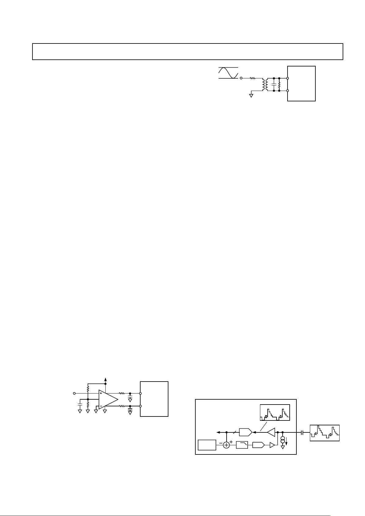
REV. 0
AD9873
–31–
lower the ac load impedance. The value of this capacitance will
depend on the source resistance and the required signal bandwidth. In systems that must use dc coupling, use an op amp to
comply with the input requirements of the AD9873.
Op Amp Selection Guide
Op amp selection for the AD9873 is highly application-dependent.
In general, the performance requirements of any given application
can be characterized by either time domain or frequency domain
constraints. In either case, one should carefully select an op amp
that preserves the performance of the ADC. This task becomes
challenging when one considers the AD9873’s high-performance
capabilities, coupled with other system-level requirements such
as power consumption and cost. The ability to select the optimal
op amp may be further complicated either by limited power supply availability and/or limited acceptable supplies for a desired
op amp. Newer high-performance op amps typically have input
and output range limitations in accordance with their lower supply
voltages. As a result, some op amps will be more appropriate in
systems where ac-coupling is allowed. When dc-coupling is
required, op amps’ headroom constraints (such as rail-to-rail op
amps) or ones where larger supplies can be used, should be
considered. Analog Devices offers differential output operational
amplifiers like the AD8131 or AD8132. They can be used for
differential or single-ended-to-differential signal conditioning with
8-bit performance to directly drive ADC inputs. The AD8138
is a higher performance version of the AD8132. It provides
12-bit performance and allows different gain settings. Please
contact the factory or local sales office for updates on Analog
Devices’ latest amplifier product offerings.
ADC Differential Inputs
The AD9873 uses 1 V p-p input span for the 8-bit ADC inputs
and 2 V p-p for the 10- and 12-bit ADCs. Since not all applications have a signal preconditioned for differential operation, there
is often a need to perform a single-ended-to-differential conversion. In systems that do not need a dc input, an RF transformer
with a center tap is the best method to generate differential inputs
beyond 20 MHz for the AD9873. This provides all the benefits
of operating the ADC in the differential mode without contributing additional noise or distortion. An RF transformer also
has the added benefit of providing electrical isolation between
the signal source and the ADC. An improvement in THD and
SFDR performance can be realized by operating the AD9873
in differential mode. The performance enhancement between
the differential and single-ended mode is most considerable as
the input frequency approaches and goes beyond the Nyquist
frequency (i.e., f
IN
> FS/2).
AINP
AINN
SINGLE-ENDED
ANALOG INPUT
R1
R1
R2
R2
AD9873
AD8131
Figure 21. Single-Ended-to-Differential Input Drive
The AD8131 provides a convenient method of converting a singleended signal to a differential signal. This is an ideal method for
generating a direct coupled signal to the AD9873. The AD8131
will accept a signal swinging below 0 V and shift it to an externally
provided common-mode voltage. The AD8131 configuration
is shown in Figure 21.
AINP
AINN
AD9873
R
R1
C
Figure 22. Transformer-Coupled Input
Figure 22 shows the schematic of a suggested transformer circuit.
Transformers with turns ratios (n
2/n1
) other than one may be
selected to optimize the performance of a given application. For
example, selecting a transformer with a higher impedance ratio
(e.g., Mini-Circuits T16–6T with an impedance ratio of (z
2/z1
)
= 16 = (n
2/n1
)2) effectively “steps up” the signal amplitude, thus
further reducing the driving requirements of the signal source. In
Figure 22, a resistor, R1, is added between the analog inputs
to match the source impedance R as in the formula R1储4kV =
(z
2/z1
)R.
ADC Voltage References
The AD9873 has three independent internal references for its
8-bit, 10-bit, and 12-bit ADCs. Both 8-bit ADCs have a 1 V p-p
input and share one internal reference source. The 10-bit and
12-bit ADCs, however, are designed for 2 V p-p input voltages with
each of them having their own internal reference. Figure 15 shows
the proper connections of the reference pins REFT and REFB.
External references may be necessary for systems that require high
accuracy gain matching between ADCs or improvements in temperature drift and noise characteristics. External references REFT
and RFB need to be centered at AVDD/2 with offset voltages
as specified:
REFT-8: AVDDIQ/2 + 0.25 V REFB-8: AVDDIQ/2 – 0.25 V
REFT-10, -12: AVDD/2 + 0.5 V REFB-10, -12: AVDD/2 – 0.5 V
A differential level of 0.5 V between the reference pins results in
a 1 V p-p ADC input level A
IN
. A differential level of 1 V between
the reference pins results in a 2 V p-p ADC input level A
IN
.
Internal reference sources can be powered down when external references are used (Register Address 02h).
Video Input
For sampling video-type waveforms, such as NTSC and PAL
signals, the Video Input channel provides black level clamping.
Figure 23 shows the circuit configuration for using the video
channel input (Pin 100). An external blocking capacitor is used
with the on-chip video clamp circuit, to level-shift the input
signal to a desired reference level. The clamp circuit automatically senses the most negative portion of the input signal, and
adjusts the voltage across the input capacitor. This forces the
black level of the input signal to be equal to the value programmed
into the clamp level register (register address 07h).
ADC
CLAMP
LEVEL
LPF
DAC
VIDEO INPUT
CLAMP LEVEL + FS/2
CLAMP LEVEL
12
BUFFER
0.1F
2A
OFFSET
AD9873
Figure 23. Video Clamp Circuit Input

REV. 0
AD9873
–32–
5
4
3
2
7
6
9
8
1
11
10
16
15
14
13
18
17
20
19
22
21
12
24
23
26
25
28
27
30
29
32
33
34
35
36
38
39
40
41
42
43
44
45
46
47
48
49
50
31
37
76
77
78
79
74
75
72
73
70
71
80
65
66
67
68
63
64
61
62
59
60
69
57
58
55
56
53
54
51
52
100
99989796959493929190898887868584838281
MQFP
TOP VIEW
(Pins Down)
VIDEO IN
AGND
IF12+
IF12–
AGND
AVDD
REFT12
REFB12
AVDD
AGND
IF10+
IF10–
AGND
AVDD
REFT10
REFB10
AVDD
AGND
Q IN+
Q IN–
Tx IQ(1)
Tx IQ(0)
DVDD
DGND
PROFILE(1)
PROFILE(0)
RESET
DVDD
DGND
DGND
SCLK
CS
SDIO
SDO
DGND Tx
DVDD Tx
PWR DOWN
REF IO
FSADJ
AGND Tx
AGND IQ
I IN+
I IN–
AGND IQ
REFT8
REFB8
AGND IQ
AVDD IQ
DRVDD
REF CLK
DRGND
DGND SD
SDELTA0
SDELTA1
DVDD SD
CA_ENABLE
CA DATA
CA CLK
DVDD OSC
OSCIN
XTAL
DGND OSC
AGND PLL
PLL FILTER
AVDD PLL
DVDD PLL
DGND PLL
AVDD Tx
Tx+
Tx–
DRGND
DRVDD
(MSB) IF(11)
IF(10)
IF(9)
IF(8)
IF(7)
IF(6)
IF(5)
IF(4)
IF(3)
IF(2)
IF(1)
IF(0)
(MSB) Rx IQ(3)
Rx IQ(2)
Rx
IQ(1)
Rx
IQ(0)
Rx
SYNC
DRGND
DRVDD
MLCK
DVDD
DGND
Tx
SYNC
(MSB) Tx
IQ(5)
Tx
IQ(4)
Tx
IQ(3)
Tx
IQ(2)
AD9873
AVDD
0.1F
10F
0.01F
0.1F
0.01F
0.01F
0.1F
0.1F
0.1F
10F
0.01F
10F 0.1F
0.1F
10F
0.1F
0.1F
0.1F
0.1F10F0.1F
0.1F
EXTERNAL
POWER SUPPLY
DECOUPLING
DGND
Tx
GND
OSC GND
AGND IQ
AGND
V
AS
V
DS
V
DR
0.1F 0.1F
10F
0.1F
10F
Figure 24. Power Supply Decoupling
POWER AND GROUNDING CONSIDERATIONS
In systems seeking to simultaneously achieve high speed and high
performance, the implementation and construction of the printed
circuit board design is often as important as the circuit design.
Proper RF techniques must be used in device selection, placement,
routing, supply bypassing, and grounding. Figure 24 illustrates
proper power supply decoupling. Split-ground technique can
be used to isolate digital and high-speed clock generation noise
from the analog front ends. The analog front end may be
further split to minimize crosstalk between the transmit and
receive sections. Noise-sensitive video-IF signals can also be
separated from the more robust IQ-ADC signal path. One common ground underneath the chip connects all ground splits and
assures short distances for ground pin connections. Figure 24
uses two separate power supplies. V
AS
powers the analog and
clock generation section of the chip while V
DS
is used for the
digital signals of the chip. An extra power supply V
DR
is only
needed in applications that require lower level digital outputs.
D
RVDD
and D
VDD
pins should be connected together for normal
mode. V
DS
(and VDR) should not be directly connected to the
power supply of noisy digital signal processing chips. It might
even be considered as an analog supply. Ferrite beads and 10 F
decoupling capacitors isolate power supplies between functional
blocks. Each supply pin is further decoupled with a 0.1 F multi-
layer ceramic capacitor that is mounted as close as possible to
the pin. In the high-speed PLL and DAC sections additional
0.01 F capacitors may be required as shown in Figure 24.

REV. 0
AD9873
–33–
EVALUATION BOARD
Hardware
The AD9873-EB is an evaluation board for the AD9873 analog
front end converter. Careful attention to layout and circuit design
allow the user to easily and effectively evaluate the AD9873 in
any application where high-resolution, and high-speed conversion
is required. This board allows the user flexibility to operate the
AD9873 in various configurations. Several jumper or solder bridge
settings are available. The ADC inputs can be differentially
driven by transformers or by an AD8138 when using connector
J8 as the only input. Differential to single-ended transmit output
options include direct transformer coupled or filtered (75 MHz)
and variable gain amplified by the AD8323. Digital transmit
(Tx) inputs are designed to be driven from various word generators
and allow for proper load termination.
Software
The AD9873-EB software provides a graphical user interface
that allows easy programming and read back of AD9873 register
settings. Three programming windows are available. The Direct
register access window allows AD9873 register write and readback in decimal, binary or hexadecimal data format. The register
map window provides a very easy, function orientated programming of AD9873 bits and registers. Programming hints appear
when the cursor is moved over an input field. Registers are
updated on every WRITE button click. The advanced register
access window allows programming of register access sequences.
Figure 25. Evaluation Board Software

REV. 0
AD9873
–34–
Figure 26. Evaluation Board Schematic First Page, AD9873 and Analog Circuitry

REV. 0
AD9873
–35–
1 2 3 4 56
A
B
C
D
6
54321
D
C
B
A
Title
Number RevisionSize
B
Date: 14-Jul-2000 Sheet of
File: D:\AD9873\evalboard3\AD9873 Rev A.ddb Drawn By:
Martin Kessler
3VD
AVDDTX
AVDDPLL
AVDDIQ
AVDD
DRVDD
DVDD
DVDDPLL
DVDDOSC
DVDDSD
GND
+
C1
10uF - 10V
+
C2
10uF - 10V
L2
Ferrite BeadL3Ferrite Bead
+
C11
10uF - 10V
+
C5
10uF - 10V
L10
Ferrite Bead
L1
Ferrite BeadL5Ferrite Bead
L6
Ferrite Bead
L9
Ferrite Bead
DVDDTX
L4
Ferrite Bead
L7
Ferrite Bead
L8
Ferrite Bead
L12
Ferrite Bead
L13
Ferrite Bead
+C9
10uF - 10V
+C10
10uF - 10V
+C12
10uF - 10V
+C13
10uF - 10V
+C14
10uF - 10V
+C15
10uF - 10V
+C6
10uF - 10V
+C7
10uF - 10V
+C8
10uF - 10V
+C3
10uF - 10V
+C4
10uF - 10V
GND
GND
GND
L11
Ferrite Bead
+
C16
10uF - 10V
+5VRX
C81
0.01uF
C43
0.1uF
C44
0.1uF
C82
0.01uF
C80
0.01uF
C79
0.01uF
C37
0.1uF
C42
0.1uF
C35
0.1uF
C34
0.1uF
C33
0.1uF
C32
0.1uF
C36
0.1uF
C38
0.1uF
C39
0.1uF
C22
0.1uF
C25
0.1uF
C28
0.1uF
C23
0.1uF
C26
0.1uF
C29
0.1uF
C31
0.1uF
C21
0.1uF
C24
0.1uF
C27
0.1uF
C30
0.1uF
C46
0.1uF
C47
0.1uF
C45
0.1uF
C41
0.1uF
C48
0.1uF
+5VTX
AD9873 Evaluation Board - Power, Digital
A
22
C40
0.1uF
+5VACON
+3.3VACON
3VDriver
+3.3VDCON
TP1
TP-LOOP
DVDD
+C17
10uF - 10V
OE1
1
I12I23I34I45I56I67I78I8
9
O811O712O613O514O415O316O217O118OE2
19
GND
10
Vcc
20
U1
74LCX541
OE1
1
I12I23I34I45I56I67I78I8
9
O811O712O613O514O415O316O217O118OE2
19
GND
10
Vcc
20
U2
74LCX541
OE1
1
I12I23I34I45I56I67I78I8
9
O811O712O613O514O415O316O217O118OE2
19
GND
10
Vcc
20
U3
74LCX541
1234567
8
16151413121110
9
RP1
22 OHM RES NET
1234567
8
16151413121110
9
RP2
22 OHM RES NET
1234567
8
16151413121110
9
RP5
22 OHM RES NET
1234567
8
16151413121110
9
RP3
22 OHM RES NET
1234567
8
16151413121110
9
RP4
22 OHM RES NET
J4
DUT_CONTROL
123
4
876
5
RP6
22 OHM RES NET
24
U4
NC7SZ04
13
2
SJP2
13
2
SJP1
D1D0D2D3D4D5D6D7D8D9D10
D11
D12
D13
D14
D15
CLK
SYNC
SDOut
SDIn
CSL
SCK
1
14
2
15
3
16
4
17
5
18
6
19
7
20
8
21
9
22
10
23
11
24
12
25
13
J7
DB25
Parallel Printer Port Connector to PC (Male)
CA_PD
CA_SLEEP
3VD
2345678
1
RP7
1k
3VD
IF[11..0]
RXIQ[3..0]
RXSYNC
MCLK
GND
R1
33
GND
GND
GND
GND
GND
GNDGND
GND
GND
3VD
3VD
3VD
Invert CLKDelay CLK
SDO
SDIO
CS
SCLK
GND
R13
22
VccFIFO
R10 R11
GND
1234567
8
J1
POWER CONN.
AD8323 decoupling
GND
2 x NC75Z04 decoupling3 x 74LCX541 deoupling
DIGITAL RECEIVE
13
2
JP1
JUMPER 3
IF0
IF1
IF2
IF3
IF4
IF5
IF6
IF7
IF8
IF9
IF10
IF11
RXIQ0
RXIQ1
RXIQ2
RXIQ3
RXSYNC
MCLK
12345678910
1112
1314
1516
1718
1920
2122
2324
2526
2728
2930
3132
3334
3536
3738
3940
4142
4344
4546
4748
4950
J2
HEADER, RT ANG, 50 PIN
SYNC
CLK
GND
TP9
TP-LOOP
AVDDTX
TP4
TP-LOOP
AVDDIQ
TP2
TP-LOOP
DRVDD
TP3
TP-LOOP
AVDD
TP8
TP-LOOP
DVDDPLL
TP5
TP-LOOP
DVDDSD
TP6
TP-LOOP
AVDDPLL
TP7
TP-LOOP
DVDDOSC
TP10
TP-LOOP
DVDDTX
Analog Devices
Figure 27. Evaluation Board Schematic Second Page, Power and Digital Circuitry

REV. 0
AD9873
–36–
Figure 28. Evaluation Board PCB, Assembly Top Side
Figure 29. Evaluation Board PCB, Top Layer

REV. 0
AD9873
–37–
Figure 30 Evaluation Board PCB, Ground Plane
Figure 31. Evaluation Board PCB, Power Plane

REV. 0
AD9873
–38–
Figure 32. Evaluation Board PCB, Bottom Layer
Figure 33. Evaluation Board PCB, Assembly Bottom Side

REV. 0
AD9873
–39–
OUTLINE DIMENSIONS
Dimensions shown in inches and (mm).
100-Lead Metric Quad Flatpack (MQFP)
(S-100C)
0.555 (14.10)
0.551 (14.00)
0.547 (13.90)
81
100
1
50
31
30
51
TOP VIEW
(PINS DOWN)
PIN 1
80
0.742 (18.85) TYP
0.486
(12.35)
TYP
0.015 (0.35)
0.009 (0.25)
0.029 (0.73)
0.023 (0.57)
0.921 (23.4)
0.906 (23.0)
0.685 (17.4)
0.669 (17.0)
0.791 (20.10)
0.787 (20.00)
0.783 (19.90)
0.134
(4.30)
MAX
SEATING
PLANE
0.004
(0.10)
MAX
0.010
(0.25)
MIN
0.041 (1.03)
0.031 (0.78)
0.110 (2.80)
0.102 (2.60)
CONTROLLING DIMENSIONS ARE IN MILLIMETERS
C01584–4.5–7/00 (rev. 0)
PRINTED IN U.S.A.
 Loading...