

REV. 0
Information furnished by Analog Devices is believed to be accurate and
reliable. However, no responsibility is assumed by Analog Devices for its
use, nor for any infringements of patents or other rights of third parties that
may result from its use. No license is granted by implication or otherwise
under any patent or patent rights of Analog Devices.
a
AD9870
One Technology Way, P.O. Box 9106, Norwood, MA 02062-9106, U.S.A.
Tel: 781/329-4700 www.analog.com
Fax: 781/326-8703 © Analog Devices, Inc., 2001
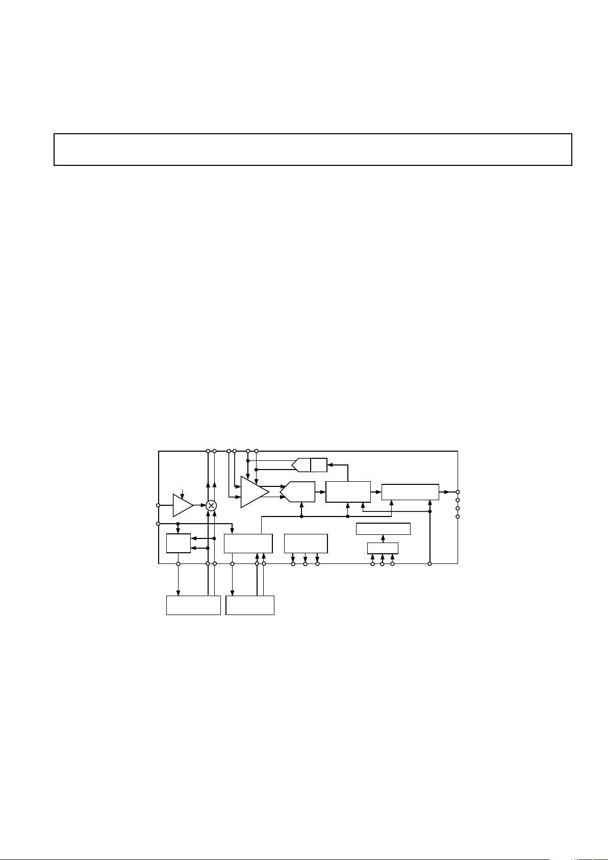
IF Digitizing Subsystem
FUNCTIONAL BLOCK DIAGRAM
IFIN
FREF
AD9870
LNA
–16dB
LO
SYNTH
IOUTL
LOP
LON
IOUTC
CLKP
CLKN
VREFP
VCM
VREFN
PC
PD
PE
SYNCB
LO VCO AND
LOOP FILTER
CLK VCO AND
LOOP FILTER
SAMP CLOCK
SYNTHESIZER
MXOP
MXON
IF2P
IF2N
GCP
GCN
DECIMATION
FILTER
CONTROL LOGIC
f
CLK
= 18MHz
- ADC
DAC
AGC
SPI
VO LTAG E
REFERENCE
FORMATTING/SSI
DOUTA
DOUTB
FS
CLKOUT
VGA /
AAF
FEATURES
10 MHz–300 MHz Input Frequency
Baseband (I/Q) Digital Output
10 kHz–150 kHz Output Signal Bandwidth
12 dB SSB NF
> –1 dBm IIP3 (High IIP3 Mode)
25 dB Continuous AGC Range + 16 dB Gain Step
Support for LO and Sampling Clock Synthesis
Programmable Decimation Rate, Output Format, AAF
Cutoff, AGC and Synthesizer Settings
360 Input Impedance
2.7 V–3.6 V Supply Voltage
Low Current: 42 mA Typ (High IIP3 Mode),
30 mA Typ (Low IIP3, Fixed Gain Mode)
48-Lead LQFP Package (1.4 mm Thick)
APPLICATIONS
Portable and Mobile Radio Products
Digital UHF/VHF FDMA Products
TETRA
PRODUCT DESCRIPTION
The AD9870 is a general-purpose IF subsystem that digitizes a
low-level 10 MHz–300 MHz IF input with a bandwidth of up to
150 kHz. The signal chain of the AD9870 consists of a low-noise
amplifier, a mixer, a variable gain amplifier with integral antialias
filter, a bandpass sigma-delta analog-to-digital converter, and a
decimation filter with programmable decimation factor. An automatic gain control (AGC) circuit provides the AD9870 with
25 dB of continuous gain adjustment. The high dynamic range
of the bandpass sigma-delta converter allows the AD9870 to
cope with blocking signals that are as much as 70 dB stronger
than the desired signal. Auxiliary blocks include clock and LO
synthesizers as well as a serial peripheral interface (SPI) port.
The SPI port programs numerous parameters of the AD9870,
including the synthesizer divide ratios, the AGC attack and decay
times, the AGC target signal level, the decimation factor, the
output data format, the 16 dB attenuator, and the bias currents of
several blocks. Reducing bias currents allows the user to reduce
power consumption at the expense of reduced performance.

REV. 0
–2–
AD9870–SPECIFICATIONS
Parameter Conditions
1
Min Typ Max Unit
OVERALL
Analog Supply Voltage
(VDDA, VDDF, VDDI) 2.7 3.0 3.6 V
Digital Supply Voltage
(VDDD, VDDC, VDDL) 2.7 3.0 3.6 V
Interface Supply Voltage
(VDDH) 1.8 3.6 V
Charge Pump Supply Voltage
(VDDP, VDDQ) 2.7 3.0 5.5 V
Total Current High IIP3 Setting 42 50.6 mA
SSB Noise Figure @ Max VGA Gain High IIP3 Setting 12 dB
Low IIP3 Setting 12 dB
Input Third-Order Intercept (IIP3) High IIP3 Setting –5 –1 dBm
Low IIP3 Setting –10 dBm
Input Impedance 360 Ω
Gain Variation Over Temperature 0.6 dB
PREAMP + MIXER
Maximum Input and LO Frequencies 300 MHz
LO SYNTHESIZER
LO Input Frequency 7.75 300 MHz
LO Input Amplitude 0.3 1.0 V p-p
FREF (Reference) Frequency 0.1 25 MHz
FREF Input Amplitude 0.3 3 V p-p
Minimum Charge Pump Output Current Programmable in 0.625 mA Steps 0.625 mA
Maximum Charge Pump Output Current Programmable in 0.625 mA Steps 5.000 mA
Charge Pump Output Compliance Voltage
2
0.25 VDDP – 0.25 V
Synthesizer Resolution 6.25 kHz
CLOCK SYNTHESIZER
CLK Input Frequency 13 18 MHz
CLK Input Amplitude Clock VCO Off 0.3 V p-p
Minimum Charge Pump Output Current Programmable in 0.625 mA Steps 0.625 mA
Maximum Charge Pump Output Current Programmable in 0.625 mA Steps 5.000 mA
Charge Pump Output Compliance Voltage
2
0.25 VDDQ – 0.25 V
Synthesizer Resolution 2.2 kHz
SIGMA-DELTA ADC
Resolution 16 Bits
Clock Frequency (f
CLK
) 13 18 MHz
Center Frequency f
CLK
/8 MHz
Dynamic Range BW = 10 kHz 88 dB
Passband Gain Variation 0.5 dB
DECIMATOR
Decimation Factor Programmable in Steps of 60 60 960
Passband Width 50 %
Passband Gain Variation 1dB
Alias Attenuation 85 dB
GAIN CONTROL
Programmable Gain Step 16 dB
AGC Gain Range (Continuous) 18 25 60 dB
AGC Attack Time Programmable 40 7000 µs
SPI
PC Clock Frequency 10 MHz
PD Hold Time 10 ns
SSI
CLKOUT Frequency 1 18 MHz
Output Rise/Fall Time CMOS Output Mode, Drive Strength = 0 120 ns
CMOS Output Mode, Drive Strength = 1 45 ns
CMOS Output Mode, Drive Strength = 2 16 ns
CMOS Output Mode, Drive Strength = 3 10 ns
OPERATING TEMPERATURE RANGE
Basic Functions –40 +95 °C
Meets All Specifications –40 +85 °C
NOTES
1
Standard operating mode: high IIP3 setting, synthesizers in normal (not fast acquire) mode, f
CLK
= 18 MHz, 25 pF load on SSI output pins: VDDx = 3.0 V.
2
Voltage span in which LO (or CLK) charge pump output current is maintained within 5% of nominal value of VDDP/2 (or VDDQ/2).
Specifications subject to change without notice.
(VDDI = VDDF = VDDA = 3.3 V, VDDC = VDDL = 3.3 V, VDDD = VDDH = 3.3 V, VDDQ =
VDDP = 5.0 V, CLK = 18 MSPS, FIF = 73.35 MHz, FLO = 71.1 MHz, unless otherwise noted.)
REV. 0
AD9870
–3–
CAUTION
ESD (electrostatic discharge) sensitive device. Electrostatic charges as high as 4000 V readily
accumulate on the human body and test equipment and can discharge without detection. Although
the AD9870 features proprietary ESD protection circuitry, permanent damage may occur on
devices subjected to high-energy electrostatic discharges. Therefore, proper ESD precautions are
recommended to avoid performance degradation or loss of functionality.
WARNING!
ESD SENSITIVE DEVICE
ABSOLUTE MAXIMUM RATINGS*
Parameter With Respect to Min Max Unit
VDDF, VDDA, VDDC, VDDD, VDDH, GNDF, GNDA, GNDC, GNDD, GNDH –0.3 +4.0 V
VDDL, VDDI GNDL, GNDI, GNDS
VDDF, VDDA, VDDC, VDDD, VDDH, VDDR, VDDA, VDDC, VDDD, VDDH, –4.0 +4.0 V
VDDL, VDDI VDDL, VDDI
VDDP, VDDQ GNDP, GNDQ –0.3 +6.0 V
GNDF, GNDA, GNDC, GNDD, GNDH GNDF, GNDA, GNDC, GNDD, GNDH –0.3 +0.3 V
GNDL, GNDI, GNDQ, GNDP, GNDS GNDL, GNDI, GNDQ, GNDP, GNDS
MXOP, MXON, LOP, LON, IFIN, GNDI –0.3 VDDI + 0.3 V
CXIF, CXVL, CXVM
PC, PD, PE, CLKOUT, DOUTA, GNDH –0.3 VDDH + 0.3 V
DOUTB, FS, SYNCB
IF2N, IF2P, GCP, GCN GNDF –0.3 VDDF + 0.3 V
VREFP, VREFN, VCM GNDA –0.3 VDDA + 0.3 V
IOUTC GNDQ –0.3 VDDQ + 0.3 V
IOUTL GNDP –0.3 VDDP + 0.3 V
CLKP, CLKN GNDC –0.3 VDDC + 0.3 V
FREF GNDL –0.3 VDDL + 0.3 V
Junction Temperature 150 °C
Storage Temperature –65 +150 °C
Lead Temperature (10 sec) 300 °C
*Stresses above those listed under Absolute Maximum Ratings may cause permanent damage to the device. This is a stress rating only; functional operation of the device
at these or any other conditions above those indicated in the operational sections of this specification is not implied. Exposure to absolute maximum ratings for extended
periods may affect device reliability.
THERMAL CHARACTERISTICS
Thermal Resistance
48-Lead LQFP
θ
JA
= 91°C/W
θ
JC
= 28°C/W
ORDERING GUIDE
Model Temperature Range Package Description Package Option
AD9870 –40°C to +85°C 48-Lead Thin Plastic Quad Flatpack (LQFP) ST-48
AD9870EB Evaluation Board
REV. 0
AD9870
–4–
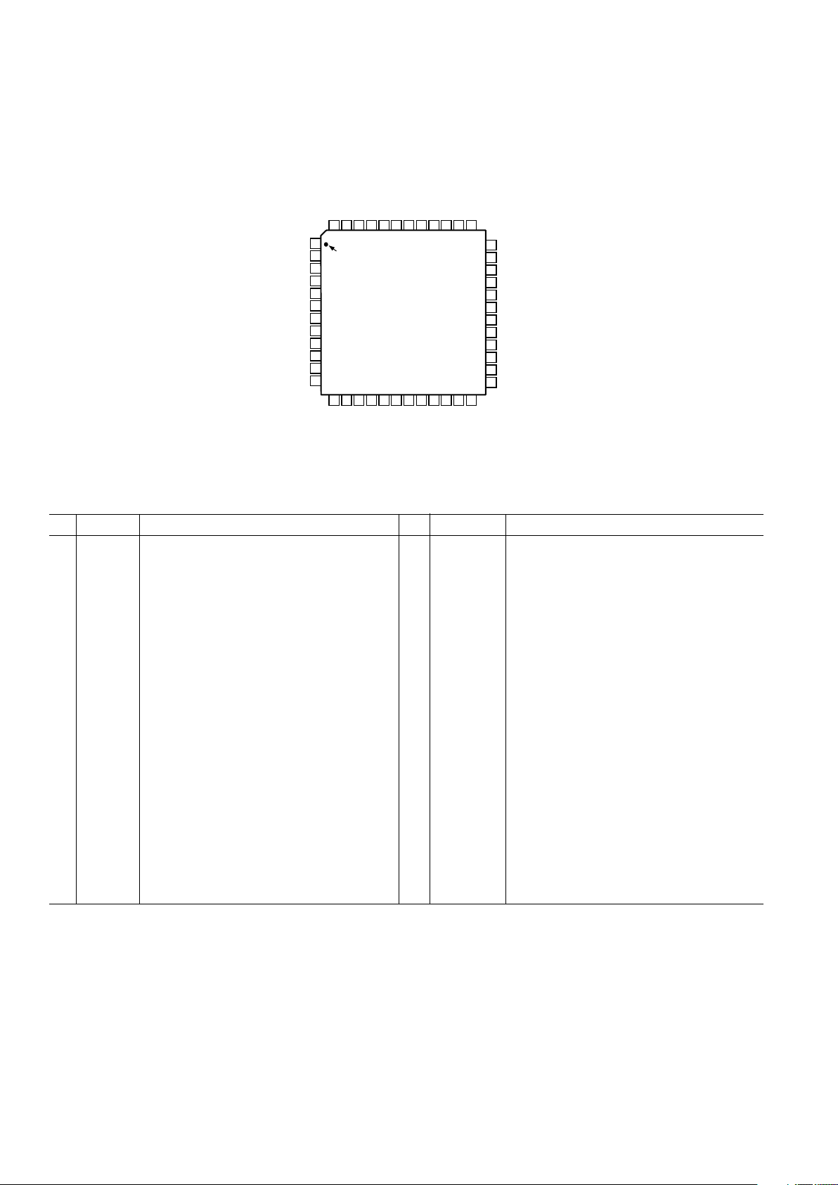
PIN FUNCTION DESCRIPTIONS
Pin Mnemonic Description Pin Mnemonic Description
1 MXOP Mixer Output, Positive 25 PE Enable Input for SPI Port
2 MXON Mixer Output, Negative 26 VDDD Positive Power Supply for Internal Digital Functions
3 GNDF Ground for VGA 27 VDDH Positive Power Supply for Digital Interface
4 IF2N Second IF Input (to VGA), Negative 28 CLKOUT Clock Output for SSI Port
5 IF2P Second IF Input (to VGA), Positive 29 DOUTA Data Output for SSI Port
6 VDDF Positive Power Supply for Antialias Filter/VGA 30 DOUTB Data Output for SSI Port, Unused
7 GCP Filter Capacitor for VGA Gain Control, Positive 31 FS Frame Sync for SSI Port
8 GCN Filter Capacitor for VGA Gain Control, Negative 32 GNDH Ground for Digital Interface
9 VDDA Positive Power Supply for ADC 33 SYNCB Resets the SSI and Decimator Counters
10 GNDA Ground for ADC 34 GNDS Substrate Ground
11 VREFP Voltage Reference, Positive 35 FREF Reference Frequency Input for Both Synthesizers
12 VREFN Voltage Reference, Negative 36 GNDL Ground for LO Synthesizer
13 VCM Common-Mode Voltage (Requires 20 kΩ to GNDA) 37 GNDP Ground for LO Synthesizer Charge Pump
14 VDDQ Pos. Power Supply for Clock Synth. Charge Pump 38 IOUTL LO Synthesizer Charge Pump Output Current
15 IOUTC Clock Synthesizer Charge Pump Output Current 39 VDDP Positive Power Supply for LO Synth. Charge Pump
16 GNDQ Ground for Clock Synthesizer Charge Pump 40 VDDL Positive Power Supply for LO Synthesizer
17 VDDC Positive Power Supply for Clock Synthesizer 41 CXVM External Capacitor for Mixer Bias
18 GNDC Ground for Clock Synthesizer 42 LON LO Input to Mixer and LO Synthesizer, Negative
19 CLKP Sampling Clock Input/Clock VCO Tank, Positive 43 LOP LO Input to Mixer and LO Synthesizer, Positive
20 CLKN Sampling Clock Input/Clock VCO Tank, Negative 44 CXVL External Capacitor for Preamp Power Supply
21 GNDS Substrate Ground 45 GNDI Ground for Mixer and Preamp
22 GNDD Ground for Digital Functions 46 CXIF External Capacitor for Preamp Bias
23 PC Clock Input for SPI Port 47 IFIN First IF Input (to Preamp)
24 PD Data I/O for SPI Port 48 VDDI Positive Power Supply for Mixer and Preamp
PIN CONFIGURATION
36
35
34
33
32
31
30
29
28
27
26
25
13 14 15 16 17 18 19 20 21 22 23 24
1
2
3
4
5
6
7
8
9
10
11
12
48 47 46 45 44 39 38 3743 42 41 40
PIN 1
IDENTIFIER
TOP VIEW
(Not to Scale)
GNDL
FREF
GNDS
SYNCB
GNDH
FS
DOUTB
MXOP
MXON
GNDF
IF2N
IF2P
VDDF
GCP
GCN
VDDA
GNDA
VREFP
DOUTA
CLKOUT
VDDH
VDDD
AD9870
VREFN
PE
VDDI
IFIN
CXIF
GNDI
CXVL
LOP
LON
CXVM
VDDL
VDDP
IOUTL
GNDP
VCM
VDDQ
IOUTC
GNDQ
VDDC
GNDC
CLKP
CLKN
GNDS
GNDD
PC
PD
REV. 0
AD9870
–5–
SERIAL PERIPHERAL INTERFACE (SPI)
The Serial Peripheral Interface (SPI) is a bidirectional serial port. It is used to load configuration information into the registers listed
below as well as to read back their contents. Table I provides a list of the registers that may be programmed through the SPI port.
Addresses and default values are given in hexadecimal form.
Table I. SPI Address Map
Address Bit
(Hex) Breakdown Width Default Value Name Description
POWER CONTROL REGISTERS
0x00 (7:0) 8 0xFF STBY Standby Control Bits (REF, LO, CKO, CK, GC, LNAMX, VGA, ADC).
0x01 (7:6) 2 0 LNAB LNA Bias Current (0 = 0.5 mA, 1 = 1 mA, 2 = 2 mA, 3 = 3 mA).
(5:4) 2 0 MIXB Mixer Bias Current (0 = 1 mA, 1 = 2 mA, 2 = 3 mA, 3 = 4 mA).
(3:2) 2 0 CKOB CK Oscillator Bias (0 = 0.25 mA, 1 = 0.35 mA, 2 = 0.53 mA, 3 = 0.85 mA).
(1:0) 2 1 ADCB ADC Amplifier Bias (0 = 2.4 mA, 1 = 3.2 mA, 2 = 4.0 mA, 3 = 4.8 mA).
0x02 (7:0) 8 0x00 TEST Factory Test Mode.
AGC
0x03 (7) 1 0 ATTEN Apply 16 dB attenuation in the front end.
(6:0) 7 0x3F AGCG(14:8) AGC Gain Setting (7 MSBs of a 15-bit two’s-complement word).
0x04 (7:0) 8 0xFF AGCG(7:0) AGC Gain Setting (8 LSBs of a 15-bit two’s-complement word).
Default corresponds to maximum gain.
0x05 (7:4) 4 0 AGCA AGC Attack Time Setting. Default yields 50 Hz raw loop bandwidth.
(3:0) 4 0 AGCD AGC Decay Time Setting. Default is decay time = attack time.
0x06 (7:4) 4 0 AGCO AGC Overload Update Setting. Default is slowest update.
(3:0) 4 0 AGCD Fast AGC (Minimizes resistance seen between GCN and GCP).
(2:0) 3 0 AGCR AGC Enable/Reference Level (disabled, 3 dB, 6 dB, 9 dB, 12 dB, 15 dB below clip).
DECIMATION FACTOR
0x07 (3:0) 4 4 M Decimation Factor = 60 × (M + 1). Default is decimate-by-300.
LO SYNTHESIZER
0x08 (5:0) 6 0x00 LOR(13:8) Reference Frequency Divisor (6 MSBs of a 14-Bit Word).
0x09 (7:0) 8 0x38 LOR(7:0) Reference Frequency Divisor (8 LSBs of a 14-Bit Word).
Default (56) Yields 300 kHz from f
REF
= 16.8 MHz.
0x0A (7:5) 3 0x5 LOA “A” Counter (Prescaler Control Counter).
(4:0) 5 0x00 LOB(12:8) “B” Counter MSBs (5 MSBs of a 13-Bit Word).
Default LOA and LOB Values Yield 300 kHz from 73.35 MHz–2.25 MHz.
0x0B (7:0) 8 0x1D LOB(7:0) “B” Counter LSBs (8 LSBs of a 13-Bit Word).
0x0C (6) 1 0 LOF Enable Fast Acquire.
(5) 1 0 LOINV Invert Charge Pump (0 = Pump_Up ⇒ IOUTL Sources Current).
(4:2) 3 0 LOI Charge Pump Current in Normal Operation. I
PUMP
= (LOI + 1) × 0.625 mA.
(1:0) 2 0 LOTM Manual Control of LO Charge Pump (3 = Off, 2 = Down, 1 = Up, 0 = Normal).
0x0D (3:0) 4 0x0 LOFA(13:8) LO Fast Acquire Time Unit (4 MSBs of a 14-Bit Word).
0x0E (7:0) 8 0x04 LOFA(7:0) LO Fast Acquire Time Unit (8 LSBs of a 14-Bit Word).
CLOCK SYNTHESIZER
0x10 (5:0) 6 00 CKR(13:8) Reference Frequency Divisor (6 MSBs of a 14-Bit Word).
0x11 (7:0) 8 0x38 CKR(7:0) Reference Frequency Divisor (8 LSBs of a 14-Bit Word).
Default Yields 300 kHz from f
REF
=16.8 MHz.
Min = 3, Max = 16383.
0x12 (4:0) 5 0x00 CKN(12:8) Synthesized Frequency Divisor (5 MSBs of a 13-Bit Word).
REV. 0
AD9870
–6–
Address Bit
(Hex) Breakdown Width Default Value Name Description
CLOCK SYNTHESIZER (Continued)
0x13 (7:0) 8 0x3C CKN(7:0) Synthesized Frequency Divisor (8 LSBs of a 13-Bit Word).
Default Yields 300 kHz from f
CLK
= 18 MHz.
Min = 3, Max = 8191.
0x14 (6) 1 0 CKF Enable Fast Acquire.
(5) 1 0 CKINV Invert Charge Pump (0 = Pump_Up ⇒ IOUTC Sources Current).
(4:2) 3 0 CKI Charge Pump Current in Normal Operation. I
PUMP
= (CKI + 1) × 0.625 mA.
(1:0) 2 0 CKTM Manual Control of CLK Charge Pump (0 = Off, 1 = Down, 2 = Up, 3 = Normal).
0x15 (3:0) 4 0x0 CKFA(13:8) CK Fast Acquire Time Unit (4 MSBs of a 14-Bit Word).
0x16 (7:0) 8 0x04 CKFA(7:0) CK Fast Acquire Time Unit (8 LSBs of a 14-Bit Word).
SSI CONTROL
0x18 (7:0) 8 0x12 SSICRA SSI Control Register A. See Table III.
(Default is FS and CLKOUT Three-Stated.)
0x19 (1:0) 2 0x0 SSICRB SSI Control Register B. See Table III.
0x1A (3:0) 4 1 SSIORD Output Rate Divisor. f
CLKOUT
= f
CLK
/SSIORD.
AAF CAPACITOR SETTING/CALIBRATION
0x1C (7:0) 8 0x00 AAR Antialias Response Selector. 0x60 Is Recommended.
0x1D 5 1 0 ERRN Error Flag.
(4:0) 5 0x0 CAPN AAF N-Well Capacitor Setting.
0x1E 5 1 0 ERRP Error Flag.
(4:0) 15 0x0 CAPP AAF Poly-Poly Capacitor Setting.
TEST REGISTERS AND SPI PORT READ ENABLE
0x38 (7:0) 8 0x00 TEST Factory Test Mode.
0x39 0 1 0 TEST Factory Test Mode.
0x3A (7:4, 2:0) 7 0x0 TEST Factory Test Mode.
(3) 1 0 SPIREN Enable Read from SPI Port.
0x3B– (7:0) 1 0x00 TEST Factory Test Mode.
0x3F

REV. 0
AD9870
–7–
PC
PE
PD
PD
WRITE OPERATION:
READ OPERATION:
A5
A5 A0
A0
D7
D7
D6
D6 D0
D0
Figure 1. SPI Timing
Figure 1 illustrates the timing for the SPI port. After the peripheral enable (PE) signal goes low, data (PD) is read on the rising
edges of the clock (PC). The first bit is a read/not-write indicator; the next six bits are address bits; the eighth bit is ignored;
the last eight bits are data. Address and data are given MSB first.
If the read/not-write indicator is a zero, a write operation occurs
and the data bits are shifted in. If the read/not-write indicator is
a one and if the read-back enable bit (Reg. 3A, Bit 3) has been
set, a read operation occurs and data is shifted out the data pin on
the falling edges of the clock. PE stays low during the operation
and goes high at the end of the transfer. If PE rises before an additional eight clock cycles have passed, the operation is aborted.
If PE stays low for an additional eight clock cycles, the destination address is incremented and another eight bits of data are
shifted in. Again, should PE rise early, the current byte is ignored.
By using this implicit addressing mode, the entire chip can be
configured with a single write operation. Registers identified as
being subject to frequent updates, namely those associated with
power control and AGC operation, have been assigned adjacent
addresses to minimize the time required to update them. The autoincrement mode is not supported for read operations.
Multibyte registers are “big-endian” (the most significant byte
has the lower address) and are updated when a write to the least
significant byte occurs.
SYNCHRONOUS SERIAL INTERFACE (SSI)
The primary output of the AD9870 is the converted signal, which
is available from the SSI port as a serial bit stream. The bit stream
consists of a 16-bit I word followed by a 16-bit Q word, where
each word is given MSB first and is in two’s-complement form.
AGC, signal strength, and synchronization information may also
be embedded in the data stream. The output bit rate (f
CLKOUT
)
is equal to the modulator clock frequency (f
CLK
) divided by
the contents of the SSIORD register. Users must verify that the
output bit rate is sufficient to accommodate the required number of bits per frame (see Table II) and that the chosen output
rate does not introduce harmful spurs. Idle (high) bits are used
to fill out each frame; the frame lengths listed in Table II
assume that with embedded frame sync (EFS = 1), at least 10
idle bits are desired.
Table II. Max Legal SSIORD Values for 16-Bit I/O Data and
Decimation by 60 n
Bits per Sample
(Min No. of Bits per Frame)
EAGC = 0 EAGC = 1
EFS =1 EFS = 0 EFS = 0 EFS = 1
32 49 48/40* 69/59*
Output
Sample Rate Max SSIORD Setting (Decimal)
Dec’n (kSPS, for EAGC = 0 EAGC = 1
M Factor f
CLK
= 18 MHz) EFS = 0 EFS = 1 EFS = 0 EFS = 1
0 60 300 1 1 1 1
1 120 150 3 2 2 1
2 180 100 5 3 3 2
3 240 75 7 4 5 3
4 300 60 9 5 6 4
5 360 50 11 7 7 5
6 420 42.857 13 8 8 5
7 480 37.5 14 9 10 6
8 540 33.333 15 10 11 7
9 600 30 15 11 12 8
10 660 27.272 15 13 13 9
11 720 25 15 14 14 10
12 780 23.077 15 15 15 11
13 840 21.428 15 15 15 11
14 900 20 15 15 15 12
15 960 18.75 15 15 15 13
*If the AAGC Bit of SSICRA is set.
Figure 2 illustrates the output timing of the SSI port for several
SSI control register settings. In the default mode of operation,
data is shifted out on rising edges of CLKOUT after a pulse is
output from the frame sync (FS) pin. As described above, the
output data consists of a 16-bit I sample followed by a 16-bit
Q sample plus two optional bytes containing AGC and status
information.

REV. 0
AD9870
–8–
The two optional bytes are output if the EAGC bit of SSICRA
is set. The first byte contains the eight most significant bits of
the AGC DAC setting while the second byte contains a 2-bit
overload field, a 2-bit reset field, a 2-bit large-signal field, a zero
bit, and a trailing high bit. The overload, reset, and large-signal
fields contain the number of overload, reset, and large-signal
events since the last report, respectively, saturating at three
should the number of events equal or exceed this amount. The
two optional bytes follow the I and Q data as a 16-bit word
provided the AAGC bit of SSICRA is not set. If the AAGC bit
is set, the two bytes follow the I and Q data in an alternating
fashion. In this “alternate AGC data” mode, the LSB of the
byte containing the AGC DAC setting is zero; the LSB of the
byte containing reset/overload information is always a one.
Figure 3 illustrates the fields of the SSI data frames.
EAGC = 0, AAGC = X: 32 DATA BITS
EAGC = 1, AAGC = 0: 48 DATA BITS
EAGC = 1, AAGC = 1: 40 DATA BITS
I (15:0) Q (15:0)
I (15:0) Q (15:0)
AGC (7:0)
1
I (15:0) Q (15:0)
AGC (7:1)
0
I (15:0) Q (15:0)
1
OVERLOAD COUNT
RESET COUNT
DON’T CARE
FGM
SAME
Figure 3. SSI Frame Structure
FS
DOUT
CLKOUT
FS
DOUT
CLKOUT
FS
DOUT
SCKI = 0, SCKT = 0, SLFS = X, SFSI = X, EFS = 1, SFST = 1, EAGC = 0
SCKI = 0, SCKT = 0, SLFS = X, SFSI = X, EFS = 1, SFST = 1, EAGC = 0: AS ABOVE, BUT FS IS LOW
IDLE (HIGH) BITS
CLKOUT
SCKI = 0, SCKT = 0, SLFS = 0, SFSI = 0, EFS = 0, SFST = 0, EAGC = 1, AAGC = 0
I15 I0 Q15 Q14 Q0 G15 G14 G0
CLKOUT
FS
DOUT
SCKI = 0, SCKT = 0, SLFS = 1, SFSI = 0, EFS = 0, SFST = 0, EAGC = 0
I15 I0 Q15 Q14 Q0
START
BIT
START
BIT
STOP
BIT
STOP
BIT
START
BIT
HI-Z
SCKI = 0, SCKT = 0, SLFS = 0, SFSI = 0, EFS = 0, SFST = 0, EAGC = 0
I15 I8 I7 I0 Q15
I15 I0 Q15 Q14 Q0
Figure 2. SSI Timing for Several SSICR Settings

REV. 0
AD9870
–9–
When the embedded frame sync bit (EFS) is set, FS is either
low or in a high Z state (as determined by the SFST bit), and
framing information is embedded in the data stream. In this
mode, each eight bits of data are surrounded by a start bit (low)
and a stop bit (high), and each frame ends with at least 10 high
bits. Other control bits can be used to invert the frame sync (SFSI),
to delay the frame sync pulse by one clock period (SLFS), to invert
the clock (SCKI), or to set the clock (SCKT) to a high Z state.
Note that if EFS is set, SLFS is a don’t care.
The AD9870 also provides the means for controlling the switching characteristics of the digital output signals. With a 25 pF
load, the rise and fall times of these signals are no more than
120 ns, 45 ns, 16 ns, or 10 ns if the DS (drive strength) setting
is 0, 1, 2, or 3, respectively.
Table III. SSI Control Registers
Name Width Description
SSICRA (ADDR = 0x18)
AAGC 1 Alternate AGC Data Bytes
EAGC 1 Embed AGC Data
EFS 1 Embed Frame Sync
SFST 1 Three-State Frame Sync
SFSI 1 Invert Frame Sync
SLFS 1 Late Frame Sync (1 = Late, 0 = Early)
SCKT 1 Three-State CLKOUT
SCKI 1 Invert CLKOUT
SSICRB (ADDR = 0x19)
DS 2 FS, CLKOUT, and DOUT Drive
Strength
POWER CONTROL
To allow power consumption to be minimized, the AD9870
possesses numerous SPI-programmable power-down and bias
control bits.
Each major block may be powered down through the appropriate bit of the STBY register. This scheme provides the greatest
flexibility for configuring the IC to a specific application as well
as for tailoring the IC’s power-down and wake-up characteristics.
Table IV summarizes the function of each of the STBY bits.
Note, when all the blocks are in standby, the master reference
circuit is also put into standby and thus the current is reduced
by a further 0.4 mA.
The AD9870 also allows control over the bias current in several
key blocks. The effects on current consumption and system
performance are described in the section dealing with the
affected block.
Table IV. Standby Control Bits
Wake-
Current Up
STBY Reduction Time
Bit Effect (mA)
1
(ms)
REF Voltage Reference Off, 1.5 1.0
VREFP, VREFN in (C
REF
=
High Z State. 4.7 µF)
LO LO Synthesizer Off, 4.8 Note 2
IOUTL in High Z State.
CKO Clock Oscillator Off. 0.25 Note 2
CK Clock Synthesizer Off, 1.4 Note 2
IOUTC in High Z State.
Clock Buffer Off if
ADC Is Off.
GC Gain Control DAC Off. 3 Depends
GCP, GCN in High Z State. on C
GC
LNAMX LNA and Mixer Off. 10
I(VDDI) = 0, CXVM,
CXVL, CXIF in High Z.
VGA VGA/AAF Off. 6 0.1
IF2P, IF2N in High Z State.
ADC ADC Off; Clock Buffer 13.8 0.1
Off if CK Synth. Off;
VCM in High Z State;
Clock-to-Digital Filter
Suspended; Digital
Outputs Static.
NOTES
1
When all blocks are in standby, the master reference circuit is also put into
standby and thus the current is reduced by a further 0.4 mA.
2
Wake-up time is application-dependent.
LO SYNTHESIZER
The LO synthesizer shown in Figure 4 is a fully programmable
PLL capable of 6.25 kHz resolution at input frequencies up to
300 MHz and reference clocks of up to 25 MHz. It consists of a
low-noise digital Phase-Frequency Detector (PFD), a variable
output current charge pump (CP), a 14-bit reference divider,
programmable A and B counters and a dual-modulus 8/9 prescaler. The A (3-bit) and B (13-bit) counters, in conjunction
with the dual 8/9 modulus prescaler, implement an N divider
with N = 8 × B + A. In addition, the 14-bit reference counter
(R Counter) allows selectable input reference frequencies, f
REF
,
at the PFD input. A complete PLL (Phase-Locked Loop) can
be implemented if the synthesizer is used with an external loop
filter and VCO (Voltage Controlled Oscillator).

REV. 0
AD9870
–10–
The A, B, and R counters can be programmed via the following
registers: LOA, LOB, and LOR. The charge pump output current
is programmable via the LOI register from 0.625 mA to 5.0 mA
using the following equation: I
PUMP
= (LOI + 1) × 0.625 mA.
An on-chip lock detect function (enabled by the LOF bit) automatically increases the output current for faster settling during
channel changes. The synthesizer may also be disabled using the
LO standby bit located in the STBY register.
FA ST
ACQUIRE
8/9
A, B
COUNTERS
LO
BUFFER
LOA, LOB
f
LO
FROM
VCO
REF
BUFFER
f
REF
LOR
R
F
REF
PHASE/
FREQUENCY
DETECTOR
TO EXTERNAL
LOOP
FILTER
f
LO
CHARGE
PUMP
Figure 4. LO Synthesizer
The LO (and CLK) Synthesizer works in the following manner.
The reference frequency, f
REF
, is buffered and divided by the
value held in the R counter. The internal F
REF
is then compared
to a divided version of the VCO frequency, f
LO
. The phase/
frequency detector provides UP and DOWN pulses whose width
vary depending upon the difference in phase and frequency of
its two input signals. The UP/DOWN pulses control the charge
pump, making current available to charge the external low-pass
loop filter when there is a discrepancy between the inputs of the
PFD. The output of the low-pass filter feeds an external VCO
whose output frequency, F
LO
, is driven such that its divided
down version, F
LO
, matches that of F
REF
thus closing the feed-
back loop.
The synthesized frequency is related to the reference frequency
and the LO register contents as follows:
f
LO
= (8 × LOB + LOA)/LOR × f
REF
Note, the minimum allowable value in the LOB register is 3 and
its value must always be greater than that loaded into LOA. The
stability, phase noise, spur performance, and transient response
of the AD9870’s LO (and CLK) synthesizers are determined by
the external loop filter, the VCO, the N-divide factor, and the
reference frequency, f
REF
. An excellent reference book on PLL
synthesizers titled PLL Performance, Simulation and Design by Deen
Banerjee is available for free at www.national.com.
An example may help illustrate how the values of LOA, LOB,
and LOR can be selected. Consider an application employing a
13 MHz crystal oscillator (i.e., f
REF
= 13 MHz) with the re-
quirement that F
REF
= 100 kHz and fLO = 143 MHz (i.e.,
high-side injection with IF = 140.75 MHz and f
SAMPLE
= 18
MSPS). LOR is selected to be 130 such that f
REF
= 100 kHz.
The N-divider factor is 1430, which can be realized by selecting LOB = 178 and LOA = 6.
Figure 5 shows the equivalent input structures of the synthesizers’ LO and REF buffers (excluding the ESD structures). The
LO input is fed to the LO synthesizers buffer as well as the
AD9870’s mixer’s LO port. Both inputs are self-biasing and
thus tolerate ac-coupled inputs. The LO input can be driven
with a single-ended or differential signal. Single-ended dccoupled inputs should ensure sufficient signal swing above and
below the common-mode bias of the LO and REF buffers (i.e.,
1.38 V and VDDL/2).
f
REF
84k
~VDDL/2
LO
BUFFER
500500
TO MIXER
LO PORT
1.36V
BIAS
LOP
LON
NOTE:
ESD DIODE STRUCTURES OMITTED FOR CLARITY
f
REF
STBY SWITCHES SHOWN WITH LO SYNTHESIZER ON
Figure 5. Equivalent Input of LO and REF Buffers
Fast Acquire Mode
The fast acquire circuit attempts to boost the output current
when the phase difference between the divided-down LO (i.e., f
LO
)
and the divided-down reference frequency (i.e., f
REF
) exceeds
the threshold determined by the LOFA register. The LOFA
register specifies a divisor for the f
REF
signal, and it is the period
(T) of this divided-down clock that specifies the time interval
which controls the fast acquire algorithm.
Assume for the moment that the nominal charge pump current
is at its lowest setting (i.e., LOI = 0) and denote this minimum
current by I
0
. When the output pulse from the phase compara-
tor exceeds T, the output current for the next pulse is 2I
0
; when
the pulse is wider than 2T, the output current for the next pulse
is 3I
0
, and so forth, up to eight times the minimum output current.
If the nominal charge pump current is more than the minimum
value (i.e., LOI > 0), the preceding rule is only applied if it results
in an increase in the instantaneous charge pump current. If the
charge pump current is set to its lowest value (LOI = 0) and the
fast acquire circuit is enabled, the instantaneous charge pump
current will never fall below 2I
0
, even when the pulsewidth is
less than T. Thus the charge pump current when fast acquire is
enabled is given by
I
PUMP-FA
= IO × (1 + max (1, LOI, Pulsewidth/T)).

REV. 0
AD9870
–11–
The recommended setting for LOFA is LOR/16. Choosing a
larger value for LOFA will increase T. Thus, for a given phase
difference between the LO input and the f
REF
input, the instantaneous charge pump current will be less than that available for
a LOFA value of LOR/16. Similarly, a smaller value for LOFA
will decrease T, making more current available for the same
phase difference. In other words, a smaller value of LOFA will
enable the synthesizer to settle faster in response to a frequency
hop than will a large LOFA value. Care must be taken to choose
a value of LOFA which is large enough (values greater than four
recommended) to prevent the loop from oscillating back and
forth in response to a frequency hop.
Table V. SPI Registers Associated with LO Synthesizer
A
ddress Bit
(Hex) Breakdown Width Default Value Name
0x00 (7:0) 8 0xFF STBY
0x08 (5:0) 6 0x00 LOR(13:8)
0x09 (7:0) 8 0x38 LOR(7:0)
0x0A (7:5) 3 0x5 LOA
(4:0) 5 0x00 LOB(12:8
0x0B (7:0) 8 0x1D LOB(7:0)
0x0C (6) 1 0 LOF
(5) 1 0 LOINV
(4:2) 3 0 LOI
(1:0) 2 0 LOTM
0x0D (3:0) 4 0x0 LOFA(13:8)
0x0E (7:0) 8 0x04 LOFA(7:0)
CLOCK SYNTHESIZER
The clock synthesizer is a fully programmable integer-N PLL
capable of 2.2 kHz resolution at clock input frequencies up to
18 MHz and reference frequencies up to 25 MHz. It is similar
to the LO synthesizer described previously in Figure 4 with the
following exceptions:
•
It does not include an 8/9 prescaler nor an A Counter.
•
It includes a negative-resistance core which when used in
conjunction with an external varactor serves as the VCO.
The 14-bit reference counter and 13-bit N-divider counter can
be programmed via the following registers: CKR and CKN. The
charge pump current is programmable via the CKI register
from 0.625 mA to 5.0 mA using the following equation:
I
PUMP
= (CKI + 1) × 0.625 mA.
The fast acquire subcircuit of the charge pump is controlled by
the CKFA register in the same manner as the LO synthesizer is
controlled by the LOFA register. An on-chip lock detect function (enabled by the CKF bit) automatically increases the output
current for faster settling during channel changes. The synthesizer may also be disabled using the CKOB standby bit located
in the STBY register.
2
CLK OSC. BIAS
I
BIAS
= 0.25, 0.35,
0.53, OR 0.85 mA
VDDC=3.0 V
IOUTC
L
OSC
0.1F
R
BIAS
C
OSC
LOOP
FILTER
C
VAR
R
D
AD9870
CLKN
CLKP
V
CM
= VDDC – R
BIAS
I
BIAS
> 1.6V
f
OSC
> (2 L
OSC
(C
VARACTOR
//C
OSC
))
–1/2
Figure 6. External Loop Filter, Varactor and L-C Tank Are
Required to Realize a Complete Clock Synthesizer
The AD9870 clock synthesizer circuitry includes a negativeresistance core so that only an external L-C tank circuit with a
varactor is needed to realize a voltage controlled oscillator (VCO).
Figure 6 shows the external components required to complete
the clock synthesizer along with the equivalent input of the CLK
input. The resonant frequency of the VCO is approximately determined by L
OSC
and the series equivalent capacitance of C
OSC
and
C
VAR
. As a result, L
OSC
, C
OSC
, and C
VAR
should be selected to
provide sufficient tuning range to ensure proper locking of the
clock synthesizer The bias, I
BIAS
, of the negative-resistance core
has four programmable settings. Lower equivalent Q of the L-C
tank circuit may require a higher bias setting of the negativeresistance core to ensure proper oscillation. R
BIAS
should be
selected such that the common-mode voltage at CLKP and
CLKN is approximately 1.6 V. The synthesizer may be disabled
via the CK standby bit to allow the user to employ an external
synthesizer and/or VCO in place of those resident on the IC.
Table VI. SPI Registers Associated with CLK Synthesizer
A
ddress Bit
(Hex) Breakdown Width Default Value Name
0x00 (7:0) 8 0xFF STBY
0x01 (3:2) 2 0 CKOB
0x10 (5:0) 6 00 CKR(13:8)
0x11 (7:0) 8 0x38 CKR(7:0)
0x12 (4:0) 5 0x00 CKN(12:8)
0x13 (7:0) 8 0x3C CKN(7:0)
0x14 (6) 1 0 CKF
(5) 1 0 CKINV
(4:2) 3 0 CKI
(1:0) 1 0 CKTM
0x15 (3:0) 4 0x0 CKFA(13:8)
0x16 (7:0) 8 0x04 CKFA(7:0)

REV. 0
AD9870
–12–
IF1 LNA/MIXER
The AD9870 contains a single-ended LNA followed by “Gilberttype” active mixer as shown in Figure 7a. The mixer’s differential
LO port is driven by an LO buffer stage which can be driven
single-ended or differential. The LO signal level can range from
0.3 V p-p to 1.0 V p-p with negligible effect on performance.
The input impedance at the IFIN pin is 360 Ω储2 pF (±20%)
and has no significant variation with respect to the programmable
bias settings. Figure 7b. shows the S11 parameters of the AD9870
with the following LNA/Mixer bias setting: LNAB = 3, MIXB = 3.
R
GAIN
R
F
R
IN
= 360
R
BIAS
LNA GAIN = 15 dB
180 180
MIXER GAIN = –5 dB
LO INPUT =
0.3 TO 1.0 V p–p
DC SERVO
LOOP
MULTI-TANH
V–I STAGE
VCML
Figure 7a. Simplified Schematic of AD9870’s LNA/Mixer
10 25
50
100
200
400
J10
–J10
J25
–J25
J50
–J50
J100
–J100
J200
–J200
J400
–J400
0
323–J105
AT 73.35 MHz
255–J163
AT 140 MHz
166–J177
AT 240 MHz
Figure 7b. Input Impedance (i.e. S11) of the AD9870’s
IF1 Input
Both the LNA and mixer have four programmable bias settings
so that current consumption can be minimized for a given application. Figures 7c, 7d, and 7e show how the LNA and mixer’s
noise figure (NF), linearity (IIP3), conversion gain, current
consumption and frequency response are all affected for a given
LNA/Mixer bias setting. The measurements were taken at an IF
= 73.35 MHz, an LO = 71.1 MHz, and supplies set to 3.0 V.
Note, since the current consumption of the LNA/Mixer portion
of the IC can be reduced by only 5 mA at most relative to the
nominal current consumption of the entire IC in the high IIP3
mode (i.e., 42 mA), most applications will benefit with the
AD9870’s LNA/Mixer configured for the high bias mode (i.e.,
LNAB = 3, MIXB = 3 for SPI Port Register 1).
LNA-MIXER POWER BIAS SETTING
12
0–0
dB
11
10
9
8
7
6
0–10–20–31–01–11–21–32–02–12–22–33–03–13–23–3
CONVERSION
GAIN
NOISE
FIGURE
Figure 7c. LNA/Mixer Noise Figure and Conversion Gain
vs. Bias Setting
LNA-MIXER POWER BIAS SETTING
5
0–0
IIP3 – dB
0
–5
–10
–15
–20
–25
0–10–20–31–01–11–21–32–02–12–22–33–03–13–23–3
LNA–MIXER
CURRENT
IIP3
CURRENT – mA
9
8
7
6
5
4
3
2
1
0
Figure 7d. LNA/Mixer IIP3 and Current Consumption vs.
Bias Setting

REV. 0
AD9870
–13–
FREQUENCY – MHz
1
10
dB
–1
–2
–3
–4
–5
–6
3–3 BIAS
SETTING
100 1000
0
2–2 BIAS
SETTING
1–1 BIAS
SETTING
0–1 BIAS
SETTING
Figure 7e. LNA/Mixer Frequency Response vs. Bias
Setting
Table VII. SPI Registers Associated with LNA/Mixer
A
ddress Bit
(Hex) Breakdown Width Default Value Name
0
x01 (7:6) 2 0 LNAB
0x01 (5:4) 2 0 MIXB
0x03 (7) 1 0 ATTEN
ANTIALIAS FILTER
The AD9870 includes a programmable continuous-time third
order antialias filter (AAF) as shown in Figure 8. Its purpose is
to suppress any noise or spectral components occurring at N ×
f
CLK
± (f
CLK
/8) from aliasing back into the sigma-delta ADC’s
passband centered at f
CLK
/8. It consists of a programmable
capacitor at the mixer output providing a real pole plus a second
order programmable filter built into the VGA providing a complex pole pair.
C2
C0
R0
180
G
m0
G
m1
C1
R1
R2
C0 AND C1 CONSIST OF 36 NWELL CAPACITORS IN PARALLEL
C3 CONSIST OF 36 POLY-POLY CAPACITORS IN PARALLEL
MIXER
(5MHz LOWPASS)
I-V 2ND ORDER LPF
Figure 8. Equivalent Circuit of Antialias Filter
The AAF is typically tuned during the start-up phase of the
AD9870. The user initiates tuning of the AAF by writing a value to
the AAR (antialias response) register. The following two considerations should be noted when tuning the AAF response. First,
the accuracy of the tuning algorithm is sensitive to on-chip
digital noise. Thus, placing the ADC in standby (i.e., register STBY)
prior to tuning the AAF is recommended. Second, although the
default setting of the AAR register is 0x00, writing 0x00 is not recom-
mended since all subsequent writes to this register will be ignored
until power to the AD9870 is reapplied to reset this register.
The AAF tuning algorithm works in the following manner. The
AD9870 measures the oscillation frequency of an on-chip RC
oscillator relative to the frequency applied to the CLKP, CLKN
pins. It then uses this measurement in conjunction with the AAR
setting to program the capacitors of the AAF which sets the filters
poles. The on-chip circuitry sets the capacitor-programming
registers (CAPN and CAPP) to the required values based on the
clock frequency and the AAR setting.
The recommended –3 dB cutoff frequency is f
CLK
/3.2 (selected
by setting AAR = 0x60) since it provides minimal signal attenuation in the passband region of f
CLK
/8 and sufficient attenuation
of the potential alias components in the transition band region.
For this setting the frequency-scaling resolution is sufficient to
yield less than 10% tuning error with clock frequencies between
13 MHz and 18 MHz. Figure 9a shows the measured response
of the antialias filter when it has been tuned with AAR = 0x60 at
an ADC clock frequency of 18 MHz. The multiple curves show
the possible tuning error due to the finite resolution of the tuning capacitors. In this example, the capacitor across the mixer
load resistors yields a pole at 5 MHz, which degrades the mixer
gain at 2.25 MHz by approximately 0.8 dB. The nominal –3 dB
cutoff frequency of the antialias filter is 5.6 MHz. The nominal
attenuation at the first alias (15.75 MHz) is 28 dB and falls at
60 dB/decade so that the nominal attenuation at 50 MHz is 60 dB.
5
FREQUENCY – MHz
0.1
AAF FREQUENCY RESPONSE – dBFS
–5
–15
–25
–35
–45
–55
–65
1 10 100
2.25MHz IF @ CLK = 18MSPS
Figure 9a. Antialias filter response with AAR = 0x60 and
f
CLK
= 18 MHz. Note, the curves have been normalized
individually to 0 dB at f
0
= 2.25 MHz.
Since the frequency measurements are performed relative to the
clock frequency, the AAF’s normalized frequency response
remains relatively independent of the ADC clock frequency.
There is guaranteed to be sufficient range in the programmable
capacitor arrays to support the response of Figure 9a for clock
frequencies between 13 MHz and 18 MHz with the resolution
indicated. Also, the normalized frequency response of the AAF
remains relatively independent of the programmed –3 dB cutoff
frequency over a 13 MHz to 18 MHz frequency range as shown
in Figure 9b. If the user specifies an unattainable response, the
on-chip circuitry sets CAPN and/or CAPP to the limit of their
ranges and also sets the ERRN and/or ERRP bit to indicate that
the specified response cannot be supported.

–14–
)
REV. 0
5
FREQUENCY – MHz
0.01
AAF FREQUENCY RESPONSE – dBFS
–5
–15
–25
–35
–45
–55
–65
0.1 1 10
–75
–85
–95
f
CLK
/8
f
CLK
= 15MSPS
f
CLK
= 18MSPS
f
CLK
= 13MSPS
Figure 9b. Measured Normalized AAF Frequency Response
for AAR = 0
×
60 Setting with f
CLK
= 13, 15, and 18 MHz
5
FREQUENCY – MHz
0.1
AAF FREQUENCY RESPONSE – dBFS
–5
–15
–25
–35
–45
–55
–65
1 10 100
AAR = 0 30
AAR = 0 60
AAR = 0 C0
Figure 9c. Measured AAF Frequency Response for Different AAR Settings with f
CLK
= 18 MHz
Changing the AAR setting from the recommended value of 0 × 60
scales the frequency axis in an inverse way as shown in Figure
9c. For example, to scale the frequency response down by a
factor of 1.5 set the AAR register to 1.5 times 0 × 60 (i.e., 0 × 90).
This AAR setting will not cause an error flag to be set for f
CLK
= 18 MHz since the 3.7 MHz cutoff is within the guaranteed
range. For f
CLK
= 18 MHz, this AAR setting would increase the
attenuation at the first alias by 10 dB, lower the –3 dB cutoff
from 5.6 MHz to 3.7 MHz, and reduce the mixer gain by 0.8 dB
due to the reduced mixer pole frequency
. However,
reducing
f
CLK
to 13 MHz while using the same AAR setting in many parts
may cause a deviation in the normalized frequency response
since the –3 dB cutoff of 2.7 MHz is well below the 3.5 MHz
lower limit. In general, –3 dB cutoff frequencies can be approximated by the following equation:
f
–3 dB
= (f
CLK
/3.2) × (0 × 60/AAR)
where AAR is the hexadecimal contents of the AAR register and
0 × 60 is its hexadecimal default setting.
Table VIII. SPI Registers Associated with AAF
Address Bit
(Hex) Breakdown Width Default Value Name
0x1C (7:0) 8 0x00 AAR
0x1D 5 1 0 ERRN
(4:0) 5 0x0 CAPN
0x1E 5 1 0 ERRP
(4:0) 15 0x0 CAPP
VARIABLE GAIN AMPLIFIER OPERATION WITH
AUTOMATIC GAIN CONTROL
The AD9870 contains a variable gain amplifier (VGA) as well as
all of the necessary signal estimation and control circuitry to
implement automatic gain control (AGC) as shown in Figure
10. The AGC control circuitry provides a high degree of programmability to allow the user to optimize the AGC response as
well as the AD9870’s dynamic range for a given application.
The VGA is programmable over a 25 dB (typ) range and implemented in the same circuitry as the AAF circuitry previously
discussed. Since its input is self-biasing and presents a high
impedance to the mixer output load, the differential output
signal appearing at the mixer output (MXOP, MXON) must be
ac coupled to the VGA input (IF2P, IF2N) with 0.1 µF ceramic
chip capacitors. Note, an external 20 k
Ω
resistor in parallel with a
0.1
µ
F capacitor from VCM (Pin 13) to GNDA is required to ensure
common-mode compatibility between the ADC input and VGA output.
The purpose of the VGA is to extend the usable dynamic range
of the AD9870 by allowing the sigma-delta ADC to digitize low
level signals in the presence of larger unfiltered interferer signals
without saturation or “clipping” the ADC. The VGA can operate in either a user controlled variable gain control mode or
automatic gain control (AGC) mode. The VGA may also be
disabled using the VGA standby bit located in the STBY register.
Note, ideally the quiescent current of the VGA circuitry should
reduced from 6 mA to 0 mA when the standby is invoked. However, it has been found that the standby current increases to
1.3 mA a few seconds (temperature dependent) after placing
the VGA in standby. Hence, the user is recommended to write
to the STBY register periodically (0.1 kSPS) and toggle the
VGA bit (i.e., write 0 followed by 1) to ensure that the standby
current remains at approximately 0 mA.
VGA
DAC
e
j(2f
CLK
/8)t
VGA /
AAF
C
DAC
GCN
GCP
IF2P
IF2N
-ADC
f
CLK
DEC1
20
20
I
Q
A
BS
(I[N])+ABS(Q[N])
AGCR
REF LEVEL
AGC
CONTROL
ADC
CLIP POINT
OLW
1
(1–Z
–1
)
f
CLK
/20
Figure 10. Functional Block Diagram of VGA and AGC

REV. 0
AD9870
–15–
Variable Gain Control
When in variable gain mode, the gain of the VGA can be adjusted
by writing to the 16-bit AGCR register. Note, proper loading of
the AGCR register requires that address 0x03 always be writ-
ten prior to 0x04. The maximum update rate of the AGCG
register is f
CLK
/100. The MSB of this register is the bit which
enables 16 dB of attenuation in the preamp. This feature
allows the AD9870 to cope with large level signals beyond
the VGA’s range to prevent overloading of the ADC.
The gain of the VGA is set by an 8-bit control DAC which
provides a differential control signal to the VGA appearing at
pins GCP and GCN. Two external 0.1 µF capacitors, C
DAC
,
from GCP and GCN to analog ground, are required to “smooth”
or filter the DAC’s output each time it updates. Note, the differential equivalent value of these two capacitors (i.e., C
DAC/2
)
in combination with the DAC’s programmable output resistance sets the –3 dB bandwidth and time constant associated
with this RC network.
Automatic Gain Control (AGC)
The gain of the VGA is automatically adjusted when the AGC is
enabled via the AGCR register. In this mode, the gain of the
VGA is continuously updated in an attempt to ensure that the
maximum signal level into the ADC does not exceed a fixed
analog ADC clip level and that the rms output level of the ADC
is equal to a programmable reference level. This programmable
level can be set at 3 dB, 6 dB, 9 dB, 12 dB, and 15 dB below
the ADC saturation (clip level) by writing values from 1 to 5 to
the 3-bit AGCR field. Note, the ADC clip level is defined to be
–2 dBFS of its full-scale (i.e., 0.28 V rms). If AGCR is 0, automatic gain control is disabled.
The AGC control loop and estimation circuitry are implemented
both in the analog and digital domain to cope with out-of-band
interferers and in-band signals which could otherwise overload
the ADC. If the largest signal into the ADC falls outside the
passband of the first stage digital filter and exceeds the ADC
clip level of –2 dBFS, a control loop based on an analog comparator is used to reduce the VGA gain and prevent ADC clipping.
If the largest signal into the ADC is the target signal (and/or
interferer) falling within the passband defined by the first decimation filter (but below the ADC clip level), a control loop
based on a digital estimation of the signal power is used to control the VGA gain.
Referring to Figure 10, an analog comparator is used to compare the VGA output (or ADC input) to a reference threshold
which is close to that of the ADC clip level. The output of the
comparator will be a digital signal named “OLW” which drives
the digital integrator within the AGC control loop when an overload condition is detected. Note, the detection of an overload
condition via this analog signal estimation path takes precedence
over the digital signal estimation path in the AGC control loop
until the analog overload condition is removed. For signals
falling within the passband of the first stage decimate-by-20
digital filter, the rms power of the I and Q signal is estimated
digitally by the following equation:
X
EST
[N] = ABS(I[N]) + ABS(Q[N]) (1)
As a result, the VGA and other registers involved in the AGC
algorithm are updated at f
CLK
/20. The number of overload and
ADC reset occurrences within the final I/Q update rate of the
AD9870 as well as the AGC value (8 MSBs) can be read from
the SSI data upon proper configuration.
A description of the AGC control algorithm and the user adjustable parameters follows. First consider the situation in which the
in-band signal is bigger than all out-of-band signals. In this case,
the amplitude of the in-band signal will be tracked to the programmed reference level by the AGC using the output of the
digital estimation block. If the difference is negative (i.e., the
signal is too large), the gain is decreased with a proportionality
constant determined by the AGCA setting. Large AGCA values
result in large gain changes thus rapid tracking of changes in
signal strength. If the difference between the target and estimated
signal level is positive (i.e., the signal is too small), the gain is
increased but now the proportionality constant is determined by
both the AGCA and AGCD settings. AGCD is effectively subtracted from AGCA, so large AGCD results in smaller gain
changes and thus slower tracking of fading signals.
The 4-bit code in the AGCA field sets the raw bandwidth of the
AGC loop. With AGCA = 0, the AGC loop bandwidth is at its
minimum of 50 Hz. Each increment of AGCA increases the
loop bandwidth by a factor of 2
1/2
; thus the maximum band-
width is 9 kHz. A general expression for the attack bandwidth is
BW
A
= 50 × (f
CLK
/18 MHz) × 2
(AGCA/2)
Hz (2)
The attack time may be estimated from the loop bandwidth if
one assumes that the loop dynamics are essentially that of a
single-pole system as described by the following equation.
t
ATTACK
= 2.2/(100 × × 2
AGCA/2
) = 0.35/BW
A
(3)
This approximation is good if the extra pole caused by the RC
filter on the DAC output is at a sufficiently high frequency. If
the RC pole is placed at four times the raw AGC pole (i.e.,
RC = 1/(8 × π × BW)) then Equation 3 yields an attack time
which is high by about 25%. A more accurate formula for this
case is to replace the 2.2 in the numerator of Equation 3 by 1.7.
The 4-bit code in the AGCD field sets the ratio of the attack
time to the decay time in the amplitude estimation circuitry.
When AGCD is zero, this ratio is one. Incrementing AGCD
multiplies the decay time-constant by 2
1/2
, allowing a 180:1
range in the decay time relative to the attack time. The decay
time may be computed from
t
DECAY
= t
ATTACK
× 2
(AGCD/2)
(4)
The 4-bit code in the AGCO field sets the weighting applied
to gain updates when overload is detected. Each increment in
AGCO doubles the weighting factor. At the highest AGCO
setting, each reset event will cause a 6 dB reduction in the
VGA gain.
Lastly, the AGCF bit reduces the DAC source resistance by a
factor of 8. This facilitates fast acquisition by lowering the RC
time constant which is formed with the external capacitors
connected from the GCP and GCN pins to ground. For an
overshoot-free step response in the AGC loop, the capacitors
should be chosen such that the RC time constant is less than
one quarter that of the raw loop. Specifically,
RC ⱕ 1/(8 π BW) (5)
where R is the resistance between the GCN and GCP pins and
ground (30 kΩ ± 30% if AGCF = 0, <3.8 kΩ if AGCF = 1) and
BW is the raw loop bandwidth. Note that with C chosen at this
upper limit, the loop bandwidth increases by approximately 30%.

REV. 0
AD9870
–16–
Table IX. SPI Registers Associated with AGC
A
d
dress Bit Default
(Hex) Breakdown Width Value Name
0x03 (7) 1 0 ATTEN
(6:0) 7 0x3F AGCG(14:8)
0x04 (7:0) 8 0xFF AGCG(7:0)
0x05 (7:4) 4 0 AGCA
(3:0) 4 0 AGCD
0x06 (7:4) 4 0 AGCO
(3:0) 4 0 AGCD
(2:0) 3 0 AGCR
System Noise Figure (NF) vs. VGA (or AGC) Control
The AD9870’s system NF is a strong function of the gain setting of the VGA. The noise present at the output of the VGA
and input of the ADC is relatively large and independent of the
VGA setting. Under small signal conditions in which the VGA is
set to its maximum gain, this noise referred back to the input of
the LNA’s input has less of an effect on raising the AD9870’s
system NF. However, under large signal conditions in which the
gain of the VGA must be reduced to prevent ADC clipping, this
noise quickly becomes a significant contributor in determining
the AD9870’s overall NF. Figure 11 shows how the NF of the
AD9870 in AGC mode remains relatively constant as an interferer signal input power is increased until its power reaches a
programmed reference level (i.e., –3 dB) at which point the NF
degrades almost 1 dB per dB as the interferer signal is increased
beyond this point, forcing the VGA gain to decrease. As a result, it
is recommended that the AGC referenced level be set to 3 (i.e.,
AGCR = 1) to maintain the best possible NF over the widest
input signal range.
INTERFERER AMPLITUDE – dBm
45
24
–85 –20–80
NOISE FIGURE – dB
–75 –70 –65 –60 –55 –50 –45 –40 –35 –30 –25
42
27
21
18
36
30
39
33
15
12
9
NOISE FIGURE
MEAN AGC VALUE
ADC CLIPS
AT –24 dBm
MEAN AGC VALUE
150
100
50
0
–50
–100
–150
Figure 11. Noise Figure vs. Interferer Signal Level with an
IF = 73.35 MHz and CLK = 18 MSPS and AGCR = 1
DECIMATION FILTER
The decimation filter consists of a complex mix by f
CLK
/8 and a
cascade of three linear phase FIR filters: DEC1, DEC2, and DEC3
as shown in Figure 12. DEC1 downsamples by a factor of 20
using a fourth-order comb filter. DEC2 also uses a fourthorder comb filter, but its decimation factor is set by the M
control register. DEC3 is a decimate-by-3 FIR filter.
M
DEC2
SINC
4
FILTER
M + 1
DEC3
FIR
FILTER
3
I
Q
COMPLEX
DATA TO
SSI PORT
COS
SIN
DATA FROM
MODULATOR
DEC1
SINC
4
FILTER
20
Figure 12. Decimation Filter Architecture
Figure 13a shows the response of the complete decimation filter
on a linear frequency axis for frequencies up to the third alias.
As this figure shows, the alias with the least attenuation is
located at the lower end of the third alias band and has an
attenuation of 83 dB.
FREQUENCY – kHz
0
–40
–100
03010 20
–20
–60
–80
7040
6050
dB
FOLDING
POINT
5kHz PASSBAND
88dB ATTENUATION
(MIN)
83dB ATTENUATION
(MIN)
>100dB ATTENUATION
Figure 13a. Frequency Response for f
CLKOUT
= 20 kHz,
Showing the First Three Alias Bands
Figure 13b shows the full response of the decimation filter with
the decimation factor set to 60 on a logarithmic frequency
scale, while Figure 13c shows the folded frequency response
on a linear frequency scale and Figure 13d shows a blowup of
the passband. The location of the cutoff frequency shown in Figure
13b is inversely proportional to the decimation factor. However,
since both DEC1 and DEC2 are fourth-order comb filters, their
combination is also a fourth-order comb filter and thus the
shapes of the frequency responses shown in Figures 13c and
13d are independent of the decimation factor.

REV. 0
AD9870
–17–
0
–20
–40
–60
–80
–100
10
–4
10
–3
10
–2
10
–1
BASEBAND FREQUENCY – Relative to
f
CLK
dB
Figure 13b. Decimator Frequency Response
0
–20
–40
–60
–80
–100
0.500.250
NORMALIZED FREQUENCY – Relative to
f
OUT
dB
Figure 13c. Folded Decimator Frequency Response
As Figure 13d shows, the gain variation across the passband
is approximately 0.4 dB. Normalization of full-scale is accurate
to within 0.4 dB across all decimation modes.
NORMALIZED FREQUENCY – Relative to
f
OUT
–40
–100
0
–20
0
–60
–80
0.25
dB
Figure 13d. Passband Frequency Response of the
Decimator
Evaluation Board and Software
The evaluation board along with its accompanying software
provide a simple means to evaluate the AD9870. The block
diagram in Figure 14 shows the major blocks of the evaluation
board. The evaluation board is designed to be flexible allowing
the user to configure it for different potential applications. The
power supply distribution block provides filtered, adjustable
voltages to the various supply pins of the AD9870. In the IF
Input signal path, component pads are available to implement
different IF impedance matching networks. The LO and CLK
signals can be externally applied or internally derived from a
user-supplied VCO Module interface daughter board. The reference for the on-chip LO and CLK synthesizers can be applied
via the external FREF input or an on-board crystal oscillator.
MIXER
OUTPUT
IF
INPUTLOINPUT
AD9870
OR
AD9874
VCO
MODULE
INTERFACE
CRYSTAL
OSCILLATOR
IDT
FIFO
(OPTIONAL)
AD9870/AD9874
POWER SUPPLY
DISTRIBUTION
EPROM
CLK
INPUT
FREF
INPUT
NI DAQ
68-PIN
CONNECTOR
XILINX
SPARTON
FPGA
Figure 14. Evaluation Board Platform
The evaluation board is designed to interface to a PC via a
National Instruments PCI-DIO-32HS digital IO card. A XILINX
FPGA formats the data between the AD987x and digital I/O
board. Software developed using National Instruments LabVIEW™
and provided as MS Windows™ executable programs is supplied
for the configuration of the SPI port registers and evaluation
of the AD9870 output data. These programs have a convenient
graphical user interface allowing for easy access to the various
SPI port configuration registers and real time frequency analysis
of output data.

REV. 0
AD9870
–18–
OUTLINE DIMENSIONS
Dimensions shown in inches and (mm).
48-Lead LQFP
(ST-48)
TOP VIEW
(PINS DOWN)
1
12
13
25
24
36
37
48
0.019 (0.5)
BSC
0.276
(7.00)
BSC
SQ
0.011 (0.27)
0.006 (0.17)
0.354 (9.00) BSC SQ
0.063 (1.60)
MAX
0.030 (0.75)
0.018 (0.45)
0.008 (0.2)
0.004 (0.09)
0
MIN
COPLANARITY
0.003 (0.08)
SEATING
PLANE
0.006 (0.15)
0.002
(
0.05
)
7
0
0.057 (1.45)
0.053 (1.35)

–19–

–20–
C01626–4.5–4/01(0)
PRINTED IN U.S.A.
 Loading...