Broadband Modem Mixed-Signal Front End
FEATURES
Low cost 3.3 V CMOS MxFE for broadband modems
12-bit DAC
2×/4× interpolation filter
200 MSPS DAC update rate
Integrated 23 dBm line driver with 19.5 dB gain control
12-bit, 80 MSPS ADC
−12 dB to +48 dB low noise RxPGA (<2.5 nV/√Hz)
Third order, programmable low-pass filter
Flexible digital data path interface
Half- and full-duplex operation
Backward-compatible with AD9975 and AD9876
Various power-down/reduction modes
Internal clock multiplier (PLL)
2 auxiliary programmable clock outputs
Available in 64-lead chip scale package or bare die
APPLICATIONS
Powerline networking
VDSL and HPNA
PWR DWN
MODE
TXEN/SYNC
TXCLK
ADIO[11:6]/
Tx
[5:0]
ADIO[5:0]/
Rx[5:0]
RXE/SYNC
RXCLK
AGC[5:0]
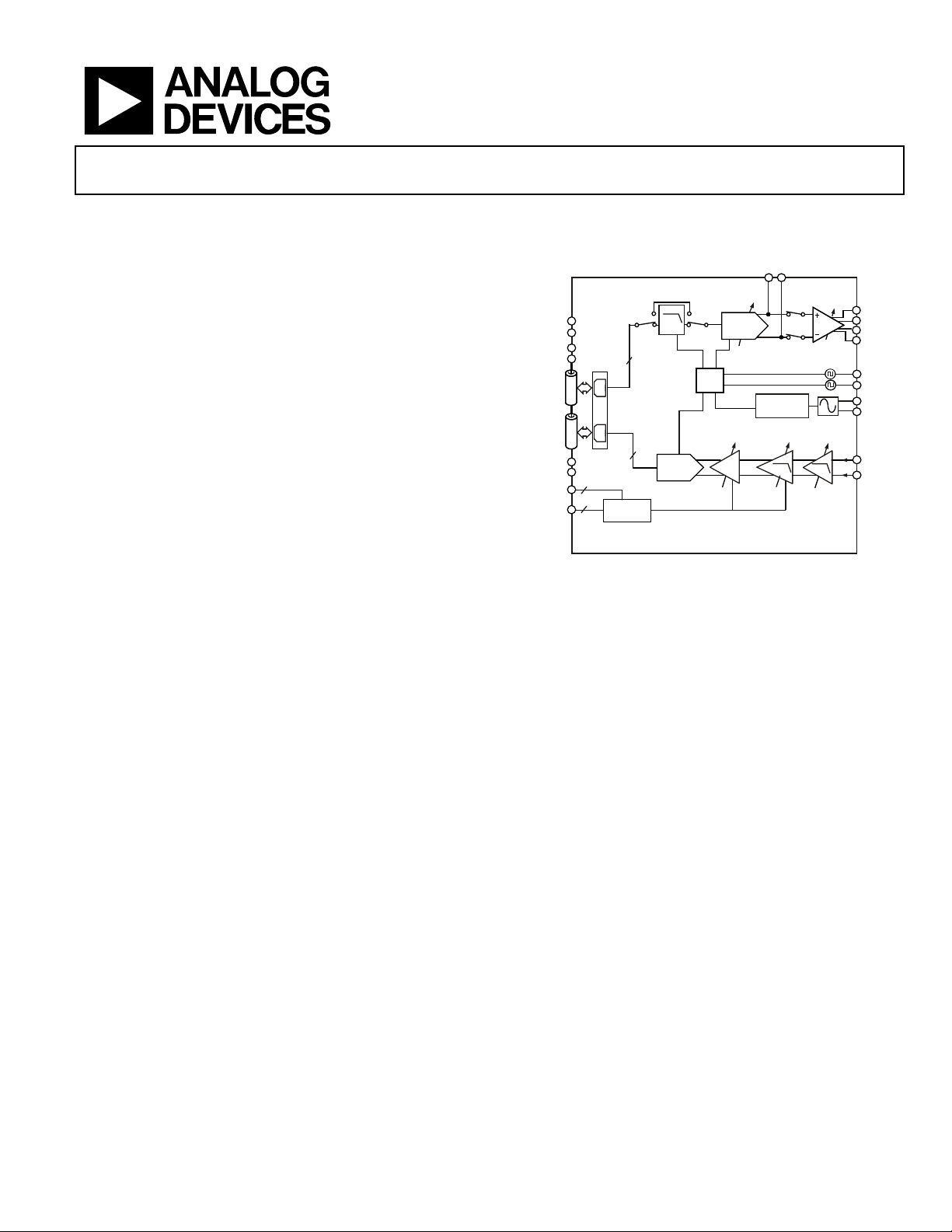
FUNCTIONAL BLOCK DIAGRAM
SPI
AD9866
6
4
REGISTER
CONTROL
2-4X
12
12
ADC
80MSPS
CLK
SYN.
0 TO 6dB
Δ = 1dB
TxDAC
0 TO –7.5dB
– 6 TO 18dB
Δ = 6dB
Figure 1.
AD9866
IOUT_P+
IOUT_P–
0 TO –12dB
2M CLK
MULTIPLIER
2-POLE
LPF
–6 TO 24dB
Δ = 6dB
IAMP
1-POLE
LPF
IOUT_G+
IOUT_N+
IOUT_N–
IOUT_G–
CLKOUT_1
CLKOUT_2
OSCIN
XTAL
RX+
RX–
04560-0-001
GENERAL DESCRIPTION
The AD9866 is a mixed-signal front end (MxFE) IC for
transceiver applications requiring Tx and Rx path functionality
with data rates up to 80 MSPS. Its flexible digital interface, power
saving modes, and high Tx-to-Rx isolation make it well-suited
for half- and full-duplex applications. The digital interface is
extremely flexible allowing simple interfaces to digital back
ends that support half- or full-duplex data transfers, thus often
allowing the AD9866 to replace discrete ADC and DAC
solutions. Power saving modes include the ability to reduce
power consumption of individual functional blocks or to power
down unused blocks in half-duplex applications. A serial port
interface (SPI®) allows software programming of the various
functional blocks. An on-chip PLL clock multiplier and
synthesizer provide all the required internal clocks, as well as
two external clocks from a single crystal or clock source.
The Tx signal path consists of a bypassable 2×/4× low-pass
interpolation filter, a 12-bit TxDAC, and a line driver. The
transmit path signal bandwidth can be as high as 34 MHz at an
input data rate of 80 MSPS. The TxDAC provides differential
current outputs that can be steered directly to an external load
or to an internal low distortion current amplifier. The current
amplifier (IAMP) can be configured as a current- or voltagemode line driver (with two external npn transistors) capable of
delivering in excess of 23 dBm peak signal power. Tx power can
be digitally controlled over a 19.5 dB range in 0.5 dB steps.
The receive path consists of a programmable amplifier
(RxPGA), a tunable low pass filter (LPF), and a 12-bit ADC.
The low noise RxPGA has a programmable gain range of
−12 dB to +48 dB in 1 dB steps. Its input referred noise is less
than 3.3 nV/√Hz for gain settings beyond 30 dB. The receive
path LPF cutoff frequency can be set over a 15 MHz to 35 MHz
range or simply bypassed. The 12-bit ADC achieves excellent
dynamic performance over a 5 MSPS to 80 MSPS span. Both
the RxPGA and the ADC offer scalable power consumption
allowing power/performance optimization.
The AD9866 provides a highly integrated solution for many
broadband modems. It is available in a space saving, 64-lead
lead frame chip scale package (LFCSP), and is specified over the
commercial (−40°C to +85°C) temperature range.
Rev. B
Information furnished by Analog Devices is believed to be accurate and reliable. However, no
responsibility is assumed by Anal og Devices for its use, nor for any infringements of patents or ot her
rights of third parties that may result from its use. Specifications subject to change without notice. No
license is granted by implication or otherwise under any patent or patent rights of Analog Devices.
Trademarks and registered trademarks are the property of their respective owners.
One Technology Way, P.O. Box 9106, Norwood, MA 02062-9106, U.S.A.
Tel: 781.329.4700 www.analog.com
Fax: 781.461.3113 ©2003–2011 Analog Devices, Inc. All rights reserved.

AD9866
TABLE OF CONTENTS
Features.............................................................................................. 1
Applications....................................................................................... 1
Functional Block Diagram ..............................................................1
General Description......................................................................... 1
Revision History ...............................................................................2
Specifications..................................................................................... 3
Tx Path Specifications.................................................................. 3
Rx Path Specifications.................................................................. 4
Power Supply Specifications........................................................ 5
Digital Specifications ................................................................... 6
Serial Port Timing Specifications............................................... 7
Half-Duplex Data Interface (ADIO Port) Timing
Specifications ................................................................................ 7
Full-Duplex Data Interface (Tx and Rx PORT) Timing
Specifications ................................................................................ 8
Absolute Maximum Ratings............................................................ 9
Thermal Characteristics ..............................................................9
Explanation of Test Levels........................................................... 9
ESD Caution.................................................................................. 9
Pin Configuration and Function Descriptions........................... 10
Typical Performance Characteristics........................................... 12
Rx Path Typical Performance Characteristics ........................12
TxDAC Path Typical Performance Characteristics ...............16
IAMP Path Typical Performance Characteristics ..................18
Serial Port ........................................................................................19
Register Map Description.......................................................... 21
Serial Port Interface (SPI)..........................................................21
Digital Interface .............................................................................. 23
Half-Duplex Mode ..................................................................... 23
Full-Duplex Mode...................................................................... 24
RxPGA Control ..........................................................................26
REVISION HISTORY
8/11—Rev. A to Rev. B
Deleted Lead Temperature Range Parameter, Table 8................. 9
Moved Explanation of Test Levels.................................................. 9
Added EPAD Note to Figure 2 and Added EPAD Note
to Table 9.......................................................................................... 10
Changes to Figure 53...................................................................... 24
Changes to Figure 54...................................................................... 25
Changes to Figure 59...................................................................... 28
TxPGA Control .......................................................................... 27
Transmit Path.................................................................................. 28
Digital Interpolation Filters...................................................... 28
TxDAC and IAMP Architecture.............................................. 29
Tx Programmable Gain Control.............................................. 30
TxDAC Output Operation........................................................ 30
IAMP Current-Mode Operation.............................................. 30
IAMP Voltage-Mode Operation............................................... 31
IAMP Current Consumption Considerations........................ 32
Receive Path ....................................................................................33
Rx Programmable Gain Amplifier........................................... 33
Low-Pass Filter............................................................................ 33
Analog-to-Digital Converter (ADC)....................................... 35
AGC Timing Considerations.................................................... 36
Clock Synthesizer ........................................................................... 37
Power Control and Dissipation.................................................... 39
Power-Down ............................................................................... 39
Half-Duplex Power Savings ...................................................... 39
Power Reduction Options......................................................... 40
Power Dissipation....................................................................... 42
Mode Select upon Power-Up and Reset.................................. 42
Analog and Digital Loopback Test Modes.............................. 43
PCB Design Considerations.......................................................... 44
Component Placement.............................................................. 44
Power Planes and Decoupling.................................................. 44
Ground Planes............................................................................ 44
Signal Routing............................................................................. 45
Evaluation Board............................................................................ 46
Outline Dimensions....................................................................... 47
Ordering Guide .......................................................................... 47
12/04—Rev. 0 to Rev. A
Changes to Specifications Tables.....................................................3
Changes to Serial Table.................................................................. 19
Changes to Full Duplex Mode section......................................... 24
Changes to Table 14 ....................................................................... 25
Change to TxDAC and IAMP Architecture section.................. 29
Change to TxDAC Output Operation section............................ 30
Insert equation................................................................................ 37
Change to Figure 84 caption......................................................... 42
11/03—Revision 0: Initial Version
Rev. B | Page 2 of 48

AD9866
SPECIFICATIONS
Tx PATH SPECIFICATIONS
AVDD = 3.3 V ± 5%, DVDD = CLKVDD = DRVDD = 3.3 V ± 10%; f
Table 1.
Parameter Temp Test Level Min Typ Max Unit
TxDAC DC CHARACTERISTICS
Resolution Full 12 Bits
Update Rate Full II 200 MSPS
Full-Scale Output Current (IOUTP_FS) Full IV 2 25 mA
Gain Error1 25°C I ±2 % FS
Offset Error 25°C V 2 μA
Voltage Compliance Range Full −1 +1.5 V
TxDAC GAIN CONTROL CHARACTERISTICS
Minimum Gain 25°C V −7.5 dB
Maximum Gain 25°C V 0 dB
Gain Step Size 25°C V 0.5 dB
Gain Step Accuracy 25°C IV Monotonic
Gain Range Error 25°C V ±2 dB
TxDAC AC CHARACTERISTICS2
Fundamental 0.5 dBm
Signal-to-Noise and Distortion (SINAD) Full IV 66.6 69.2 dBc
Signal-to-Noise Ratio (SNR) Full IV 68.4 69.8 dBc
Total Harmonic Distortion (THD) Full IV −79 −68.7 dBc
Spurious-Free Dynamic Range (SFDR) Full IV 68.5 81 dBc
IAMP DC CHARACTERISTICS
IOUTN Full-Scale Current = IOUTN+ + IOUTN− Full IV 2 105 mA
IOUTG Full-Scale Current = IOUTG+ + IOUTG− Full IV 2 150 mA
AC Voltage Compliance Range Full IV 1 7 V
IAMPN AC CHARACTERISTICS3
Fundamental 25°C 13 dBm
IOUTN SFDR (Third Harmonic) Full IV 43.3 45.2 dBc
IAMP GAIN CONTROL CHARACTERISTICS
Minimum Gain 25°C V −19.5 dB
Maximum Gain 25°C V 0 dB
Gain Step Size 25°C V 0.5 dB
Gain Step Accuracy 25°C IV Monotonic dB
IOUTN Gain Range Error 25°C V 0.5 dB
REFERENCE
Internal Reference Voltage4
Reference Error Full V 0.7 3.4 %
Reference Drift Full V 30 ppm/oC
Tx DIGITAL FILTER CHARACTERISTICS (2× INTERPOLATION)
Latency (Relative to 1/f
) Full V 43 Cycles
DAC
−0.2 dB Bandwidth Full V 0.2187 f
−3 dB Bandwidth Full V 0.2405 f
Stop-Band Rejection (0.289 f
to 0.711 f
DAC
) Full V 50 dB
DAC
Tx DIGITAL FILTER CHARACTERISTICS (4× Interpolation)
Latency (Relative to 1/f
) Full V 96 Cycles
DAC
−0.2 dB Bandwidth Full V 0.1095 f
−3 dB Bandwidth Full V 0.1202 f
Stop Band Rejection (0.289 f
OSCIN
to 0.711 f
) Full V 50 dB
OSCIN
= 50 MHz, f
OSCIN
= 200 MHz, R
DAC
= 2.0 kΩ, unless otherwise noted.
SET
25°C I 1.23 V
OUT/fDAC
OUT/fDAC
OUT/fDAC
OUT/fDAC
Rev. B | Page 3 of 48

AD9866
Parameter Temp Test Level Min Typ Max Unit
PLL CLK MULTIPLIER
OSCIN Frequency Range Full IV 5 80 MHz
Internal VCO Frequency Range Full IV 20 200 MHz
Duty Cycle Full II 40 60 %
OSCIN Impedance 25°C V 100//3 ΜΩ//pF
CLKOUT1 Jitter5
CLKOUT2 Jitter6 25°C III 6 ps rms
CLKOUT1 and CLKOUT2 Duty Cycle7 Full III 45 55 %
1
Gain error and gain temperature coefficients are based on the ADC only (with a fixed 1.23 V external reference and a 1 V p-p differential analog input).
2
TxDAC IOUTFS = 20 mA, differential output with 1:1 transformer with source and load termination of 50 Ω, F
3
IOUN full-scale current = 80 mA, f
4
Use external amplifier to drive additional load.
5
Internal VCO operates at 200 MHz , set to divide-by-1.
6
Because CLKOUT2 is a divided down version of OSCIN, its jitter is typically equal to OSCIN.
7
CLKOUT2 is an inverted replica of OSCIN, if set to divide-by-1.
= 80 MHz, f
OSCIN
=160 MHz, 2× interpolation.
DAC
Rx PATH SPECIFICATIONS
AVDD = 3.3 V ± 5%, DVDD = CLKVDD = DRVDD = 3.3 V ± 10%; half- or full-duplex operation with CONFIG = 0 default power bias
settings, unless otherwise noted.
Table 2.
Parameter Temp Test Level Min Typ Max Unit
Rx INPUT CHARACTERISTICS
Input Voltage Span (RxPGA gain = −10 dB) Full III 6.33 V p-p
Input Voltage Span (RxPGA gain = +48 dB) Full III 8 mV p-p
Input Common-Mode Voltage 25°C III 1.3
Differential Input Impedance 25°C III 400 Ω
4.0 pF
Input Bandwidth (with RxLPF Disabled, RxPGA = 0 dB) 25°C III 53 MHz
Input Voltage Noise Density (RxPGA Gain = 36 dB, f
Input Voltage Noise Density (RxPGA Gain = 48 dB, f
RxPGA CHARACTERISTICS
Minimum Gain 25°C III −12 dB
Maximum Gain 25°C III 48 dB
Gain Step Size 25°C III 1 dB
Gain Step Accuracy 25°C III Monotonic dB
Gain Range Error 25°C III 0.5 dB
RxLPF CHARACTERISTICS
Cutoff Frequency (f
Attenuation at 55.2 MHz with f
) range Full III 15 35 MHz
−3 dBF
= 21 MHz 25°C III 20 dB
−3 dBF
Pass-Band Ripple 25°C III ±1 dB
Settling Time to 5 dB RxPGA Gain Step @ f
Settling Time to 60 dB RxPGA Gain Step @ f
= 50 MSPS 25°C III 20 ns
ADC
= 50 MSPS 25°C III 100 ns
ADC
ADC DC CHARACTERISTICS
Resolution NA NA 12 Bits
Conversion Rate FULL II 5 80 MSPS
= 26 MHz) 25°C III 2.7 nV/√Hz
−3 dBF
= 26 MHz)
−3 dBF
25°C III 12 ps rms
= 5 MHz, 4× interpolation.
OUT
V
25°C III 2.4 nV/√Hz
Rev. B | Page 4 of 48
AD9866
Parameter Temp Test Level Min Typ Max Unit
Rx PATH LATENCY1
Full-Duplex Interface Full V 10.5 Cycles
Half-Duplex Interface Full V 10.0 Cycles
Rx PATH COMPOSITE AC PERFORMANCE @ f
= 50 MSPS2
ADC
RxPGA Gain = 48 dB (Full-Scale = 8.0 mV p-p)
Signal-to-Noise (SNR) 25°C III 43.7 dBc
Total Harmonic Distortion (THD) 25°C III −71 dBc
RxPGA Gain = 24 dB (Full-Scale = 126 mV p-p)
Signal-to-Noise (SNR) 25°C III 63.1 dBc
Total Harmonic Distortion (THD) 25°C III −67.2 dBc
RxPGA Gain = 0 dB (Full-Scale = 2.0 V p-p)
Signal-to-Noise (SNR) Full IV 64.3 dBc
Total Harmonic Distortion (THD) Full IV −67.3 dBc
Rx PATH COMPOSITE AC PERFORMANCE @ f
= 80 MSPS3
ADC
RxPGA Gain = 48 dB (Full-Scale = 8.0 m V p-p)
Signal-to-Noise (SNR) 25°C III 41.8 dBc
Total Harmonic Distortion (THD) 25°C III −67 dBc
RxPGA Gain = 24 dB (Full-Scale = 126 m V p-p)
Signal-to-Noise (SNR) 25°C III 58.6 dBc
Total Harmonic Distortion (THD) 25°C III −62.9 dBc
RxPGA Gain = 0 dB (Full-Scale = 2.0 V p-p)
Signal-to-Noise (SNR) 25°C II 61.1 62.9 dBc
Total Harmonic Distortion (THD) 25°C II −70.8 −60.8 dBc
Rx-to-Tx PATH FULL-DUPLEX ISOLATION
(1 V p-p, 10 MHz Sine Wave Tx Output)
RxPGA Gain = 40 dB
IOUTP± Pins to RX± Pins 25°C III 83 dBc
IOUTG± Pins to RX± Pins 25°C III 37 dBc
RxPGA Gain = 0 dB
IOUTP± Pins to RX± Pins 25°C III 123 dBc
IOUTG± Pins to RX± Pins 25°C III 77 dBc
1
Includes RxPGA, ADC pipeline, and ADIO bus delay relative to f
2
fIN = 5 MHz, AIN = −1.0 dBFS , LPF cutoff frequency set to 15.5 MHz with Reg. 0x08 = 0x80.
3
fIN = 5 MHz, AIN = −1.0 dBFS , LPF cutoff frequency set to 26 MHz with Reg. 0x08 = 0x80.
ADC
.
POWER SUPPLY SPECIFICATIONS
AVDD = 3.3 V, DVDD = CLKVDD = DRVDD = 3.3 V; R
Table 3.
Parameter Temp Test Level Min Typ Max Unit
SUPPLY VOLTAGES
AVDD Full V 3.135 3.3 3.465 V
CLKVDD Full V 3.0 3.3 3.6 V
DVDD Full V 3.0 3.3 3.6 V
DRVDD Full V 3.0 3.3 3.6 V
IS_TOTAL (Total Supply Current) Full II 406 475 mA
POWER CONSUMPTION
I
AVDD
I
DVDD
+ I
+ I
(Analog Supply Current)
CLKVDD
(Digital Supply Current) Full IV 95 133 mA
DRVDD
= 2 kΩ, full-duplex operation with f
SET
Rev. B | Page 5 of 48
IV 311 342 mA
= 80 MSPS,1 unless otherwise noted.
DATA

AD9866
Parameter Temp Test Level Min Typ Max Unit
POWER CONSUMPTION (Half-Duplex Operation with f
Tx Mode
I
AVDD
I
DVDD
+ I
+ I
25°C IV 112 130 mA
CLKVDD
25°C IV 46 49.5 mA
DRVDD
Rx Mode
I
AVDD
I
DVDD
+ I
+ I
25°C
CLKVDD
25°C
DRVDD
POWER CONSUMPTION OF FUNCTIONAL BLOCKS2 (I
RxPGA and LPF 25°C III 87 mA
ADC 25°C III 108 mA
TxDAC 25°C III 38 mA
IAMP (Programmable) 25°C III 10 120 mA
Reference 25°C III 170 mA
CLK PLL and Synthesizer 25°C III 107 mA
MAXIMUM ALLOWABLE POWER DISSIPATION Full IV 1.66 W
STANDBY POWER CONSUMPTION
IS_TOTAL (Total Supply Current) Full
POWER-DOWN DELAY (USING PWR_DWN PIN)
RxPGA and LPF 25°C III 440 ns
ADC 25°C III 12 ns
TxDAC 25°C III 20 ns
IAMP 25°C III 20 ns
CLK PLL and Synthesizer 25°C III 27 ns
POWER-UP DELAY (USING PWR_DWN PIN)
RxPGA and LPF 25°C III 7.8 μs
ADC 25°C III 88 ns
TxDAC 25°C III 13 μs
IAMP 25°C III 20 ns
CLK PLL and Synthesizer 25°C III 20 μs
1
Default power-up settings for MODE = LOW and CONFIG = LOW.
2
Default power-up settings for MODE = HIGH and CONFIG = LOW, IOUTP_FS = 20 mA, does not include IAMP’s current consumption, which is application dependent.
= 50 MSPS)1
DATA
AVDD
+ I
)
CLKVDD
225 253 mA
36.5 39 mA
13 mA
DIGITAL SPECIFICATIONS
AVDD = 3.3 V ± 5%, DVDD = CLKVDD = DRVDD = 3.3 V ± 10%; R
Table 4.
Parameter Temp Test Level Min Typ Max Unit
CMOS LOGIC INPUTS
High Level Input Voltage Full VI DRVDD – 0.7 V
Low Level Input Voltage Full VI 0.4 V
Input Leakage Current 12 μA
Input Capacitance Full VI 3 pF
CMOS LOGIC OUTPUTS (C
= 5 pF)
LOAD
High Level Output Voltage (IOH = 1 mA) Full VI DRVDD – 0.7 V
Low Level Output Voltage (IOH = 1 mA) Full VI 0.4 V
Output Rise/Fall Time (High Strength Mode and C
Output Rise/Fall Time (Low Strength Mode and C
Output Rise/Fall Time (High Strength Mode and C
Output Rise/Fall Time (Low Strength Mode and C
= 15 pF) Full VI 1.5/2.3 ns
LOAD
= 15 pF) Full VI 1.9/2.7 ns
LOAD
= 5 pF) Full VI 0.7/0.7 ns
LOAD
= 5 pF) Full VI 1.0/1.0 ns
LOAD
RESET
Minimum Low Pulse Width (Relative to f
) 1 Clock cycles
ADC
Rev. B | Page 6 of 48
= 2 kΩ, unless otherwise noted.
SET

AD9866
SERIAL PORT TIMING SPECIFICATIONS
AVDD = 3.3 V ± 5%, DVDD = CLKVDD = DRVDD = 3.3 V ± 10%, unless otherwise noted.
Table 5.
Parameter Temp Test Level Min Typ Max Unit
WRITE OPERATION (See Figure 46)
SCLK Clock Rate (f
SCLK Clock High (tHI) Full IV 14 ns
SCLK Clock Low (t
SDIO to SCLK Setup Time (tDS) Full IV 14 ns
SCLK to SDIO Hold Time (tDH) Full IV 0 ns
SEN to SCLK Setup Time (tS)
SCLK to SEN Hold Time (tH)
READ OPERATION (See Figure 47 and Figure 48)
SCLK Clock Rate (f
SCLK Clock High (tHI) Full IV 14 ns
SCLK Clock Low (t
SDIO to SCLK Setup Time (tDS) Full IV 14 ns
SCLK to SDIO Hold Time (tDH) Full IV 0 ns
SCLK to SDIO (or SDO) Data Valid Time (tDV) Full IV 14 ns
SEN to SDIO Output Valid to Hi-Z (tEZ)
) Full IV 32 MHz
SCLK
) Full IV 14 ns
LOW
Full IV 14 ns
Full IV 0 ns
) Full IV 32 MHz
SCLK
) Full IV 14 ns
LOW
Full IV 2 ns
HALF-DUPLEX DATA INTERFACE (ADIO PORT) TIMING SPECIFICATIONS
AVDD = 3.3 V ± 5%, DVDD = CLKVDD = DRVDD = 3.3 V ± 10%, unless otherwise noted.
Table 6.
Parameter Temp Test Level Min Typ Max Unit
READ OPERATION1 (See Figure 50)
Output Data Rate Full II 5 80 MSPS
Three-State Output Enable Time (t
Three-State Output Disable Time (t
) Full II 3 ns
PZL
) Full II 3
PLZ
Rx Data Valid Time (tVT) Full II 1.5 ns
Rx Data Output Delay (tOD) Full II 4 ns
WRITE OPERATION (See Figure 49)
Input Data Rate (1× Interpolation) Full II 20 80 MSPS
Input Data Rate (2× Interpolation) Full II 10 80 MSPS
Input Data Rate (4× Interpolation) Full II 5 50 MSPS
Tx Data Setup Time (tDS) Full II 1 ns
Tx Data Hold Time (tDH) Full II 2.5 ns
Latch Enable Time (tEN) Full II 3 ns
Latch Disable Time (t
1
C
= 5 pF for digital data outputs.
LOAD
) Full II 3 ns
DIS
ns
Rev. B | Page 7 of 48

AD9866
FULL-DUPLEX DATA INTERFACE (Tx AND Rx PORT) TIMING SPECIFICATIONS
AVDD = 3.3 V ± 5%, DVDD = CLKVDD = DRVDD = 3.3 V ± 10%, unless otherwise noted.
Table 7.
Parameter Temp Test Level Min Typ Max Unit
Tx PATH INTERFACE (See Figure 53)
Input Nibble Rate (2× Interpolation) Full II 20 160 MSPS
Input Nibble Rate (4× Interpolation) Full II 10 100 MSPS
Tx Data Setup Time (tDS) Full II 2.5 ns
Tx Data Hold Time (tDH) Full II 1.5 ns
Rx PATH INTERFACE1 (See Figure 54)
Output Nibble Rate Full II 10 160 MSPS
Rx Data Valid Time (tDV) Full II 3 ns
Rx Data Hold Time (tDH) Full II 0 ns
1
C
= 5 pF for digital data outputs.
LOAD
Rev. B | Page 8 of 48
AD9866
ABSOLUTE MAXIMUM RATINGS
Table 8.
Parameter Rating
ELECTRICAL
AVDD, CLKVDD Voltage 3.9 V maximum
DVDD, DRVDD Voltage 3.9 V maximum
RX+, RX−, REFT, REFB −0.3 V to AVDD + 0.3 V
IOUTP+, IOUTP− −1.5 V to AVDD + 0.3 V
IOUTN+, IOUTN−, IOUTG+, IOUTG− −0.3 V to 7 V
OSCIN, XTAL −0.3 V to CLVDD + 0.3 VS
REFIO, REFADJ −0.3 V to AVDD + 0.3 V
Digital Input and Output Voltage −0.3 V to DRVDD + 0.3 V
Digital Output Current 5 mA maximum
ENVIRONMENTAL
Operating Temperature Range
(Ambient)
Maximum Junction Temperature 125°C
Storage Temperature Range
(Ambient)
−40°C to +85°C
−65°C to +150°C
Stresses above those listed under Absolute Maximum Ratings
may cause permanent damage to the device. This is a stress
rating only; functional operation of the device at these or any
other conditions above those indicated in the operational
section of this specification is not implied. Exposure to absolute
maximum rating conditions for extended periods may affect
device reliability.
THERMAL CHARACTERISTICS
Thermal Resistance: 64-lead LFCSP (4-layer board).
θ
= 24°C/W (paddle soldered to ground plane, 0 LPM air).
JA
θ
= 30.8°C/W (paddle not soldered to ground plane, 0 LPM air).
JA
EXPLANATION OF TEST LEVELS
I 100% production tested.
II
100% production tested at 25°C and guaranteed by design
and characterization at specified temperatures.
III Sample tested only.
IV
Parameter is guaranteed by design and characterization
testing.
V Parameter is a typical value only.
VI
100% production tested at 25°C and guaranteed by design
and characterization for industrial temperature range.
ESD CAUTION
Rev. B | Page 9 of 48
AD9866
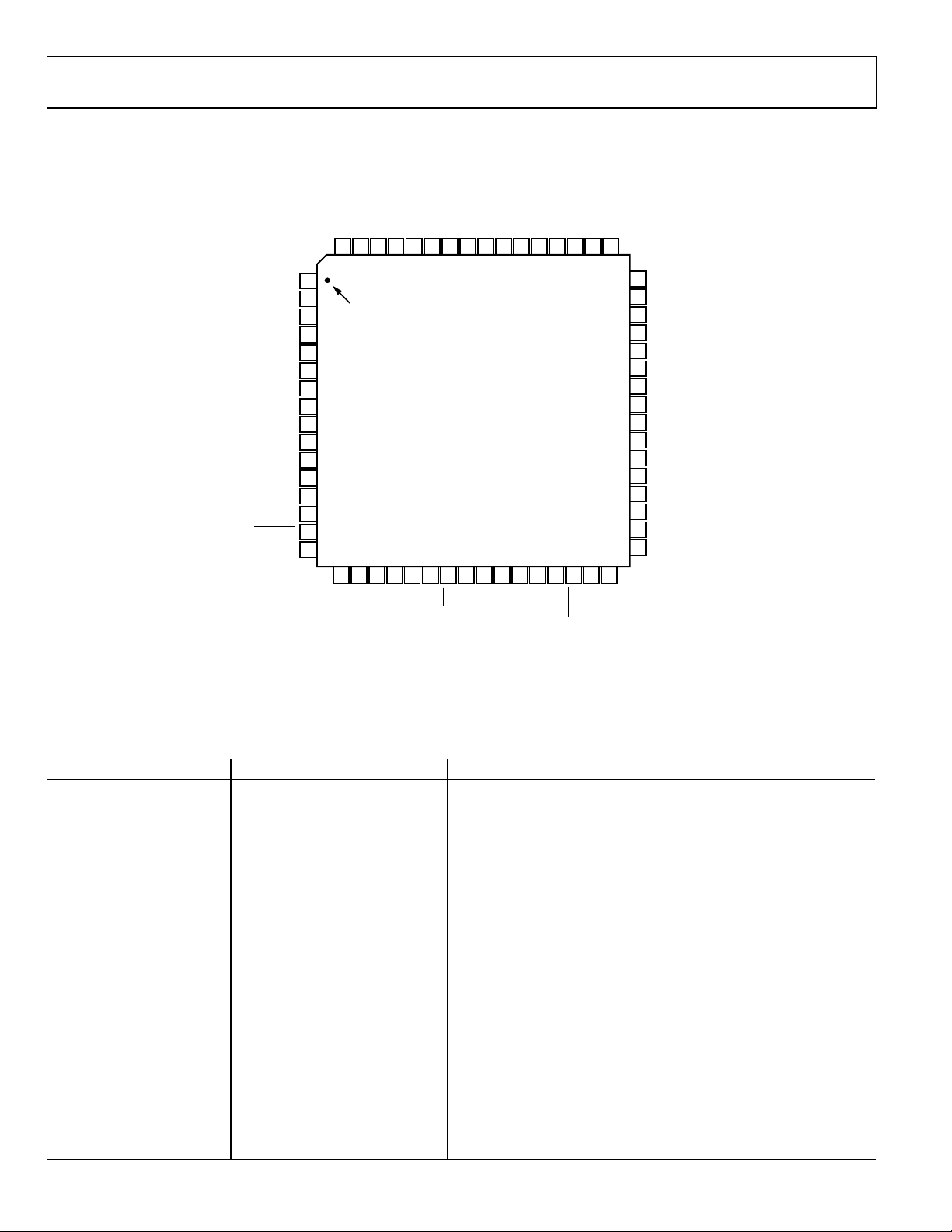
PIN CONFIGURATION AND FUNCTION DESCRIPTIONS
DRVDD
DRVSS
PWR_DWN
CLKOUT2
DVDD
DVSS
CLKVDD
OSCIN
XTAL
CLKVSS
CONFIG
ADIO11/Tx[5]
ADIO10/Tx[4]
ADIO9/Tx[3]
ADIO8/Tx[2]
ADIO7/Tx[1]
ADIO6/Tx[0]
ADIO5/Rx[5]
ADIO4/Rx[4]
ADIO3/Rx[3]
ADIO2/Rx[2]
ADIO1/Rx[1]
ADIO0/Rx[0]
RXEN/RXSYNC
TXEN/TXSYNC
TXCLK/TXQUIET
RXCLK
MODE
64
63 62 61 60 595857 56 55 54 535251 50
1
2
PIN 1
3
IDENTIFIER
4
5
6
7
8
9
10
11
12
13
14
15
16
AD9866
TOP VIEW
(Not to Scale)
IOUT_P+
IOUT_G+
IOUT_N+
IOUT_P–
49
48
AVSS
AVSS
47
46
IOUT_N–
45
IOUT_G–
44
AVSS
43
AVDD
42
REFIO
41
REFADJ
40
AVDD
39
AVSS
38
RX+
37
RX–
AVSS
36
35
AVDD
34
AVSS
REFT
33
3217 18 19 20 21 22 23 24 25 26 27 282930 31
SEN
SDO
SDIO
DRVSS
DRVDD
CLKOUT1
NOTES
1. THE EXPOSED PAD MUST BE SOLDERED TO GND.
SCLK
PGA[4]
PGA[3]
PGA[2]
PGA[1]
PGA[0]
GAIN/PGA[5]
RESET
AVSS
REFB
Figure 2. Pin Configuration
Table 9. Pin Function Descriptions
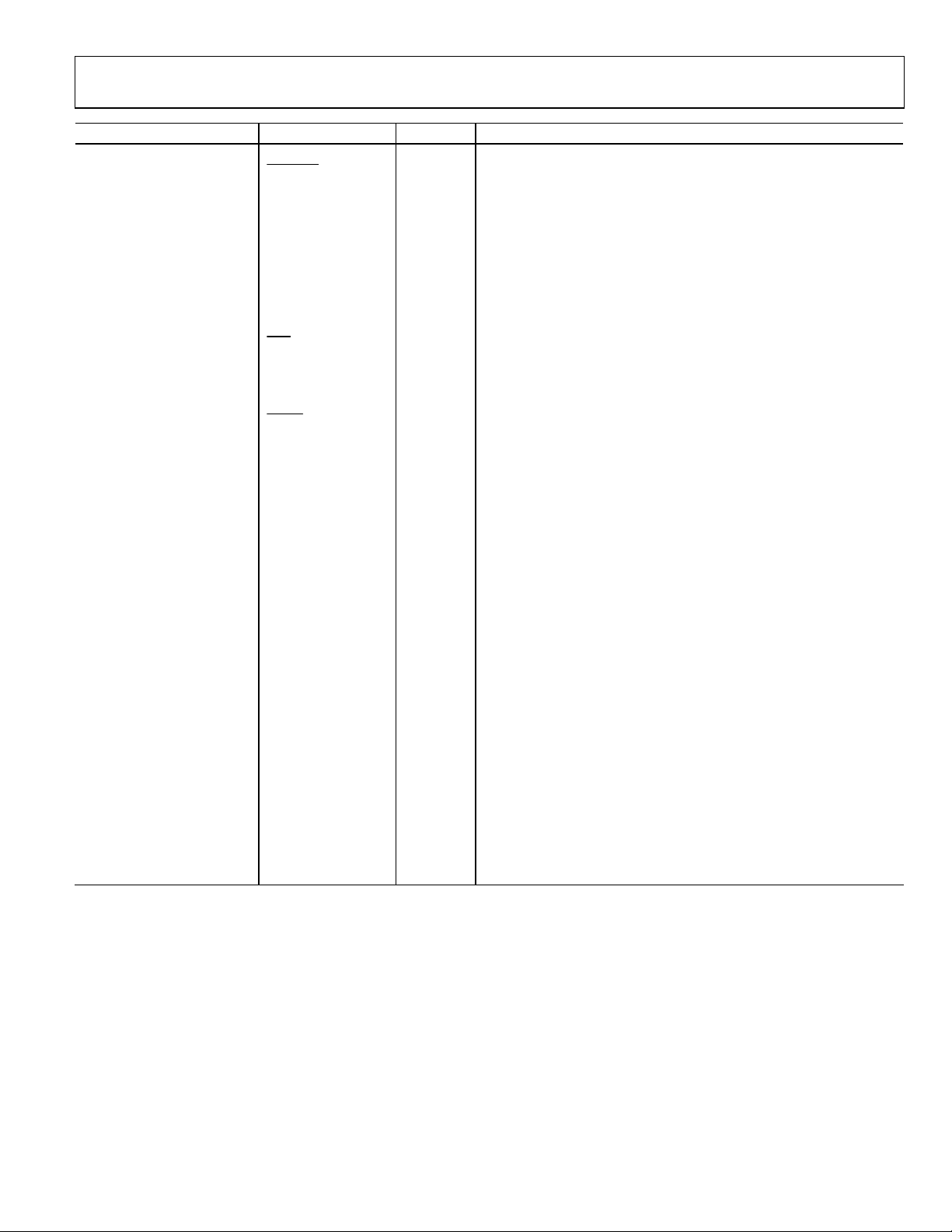
Pin No. Mnemonic Mode1 Description
1 ADIO11 HD MSB of ADIO Buffer
Tx[5] FD MSB of Tx Nibble Input
2 to 5 ADIO10 to 7 HD Bits 10 to 7 of ADIO Buffer
Tx[4 to 1] FD Bits 4 to 1 of Tx Nibble Input
6 ADIO6 HD Bit 6 of ADIO Buffer
Tx[0] FD LSB of Tx Nibble Input
7 ADIO5 HD Bit 5 of ADIO Buffer
Rx[5] FD MSB of Rx Nibble Output
8, 9 ADIO4, 3 HD Bits 4 to 3 of ADIO Buffer
Rx[4, 3] FD Bits 4 to 3 of Rx Nibble Output
10 ADIO2 HD Bit 2 of ADIO Buffer
Rx[2] FD Bit 2 of Rx Nibble Output
11 ADIO1 HD Bit 1 of ADIO Buffer
Rx[1] FD Bit 1 of Rx Nibble Output
12 ADIO0 HD LSB of ADIO Buffer
Rx[0] FD LSB of Rx Nibble Output
13 RXEN HD ADIO Buffer Control Input
RXSYNC FD Rx Data Synchronization Output
14 TXEN HD Tx Path Enable Input
TXSYNC FD Tx Data Synchronization Input
Rev. B | Page 10 of 48
04560-0-002
AD9866
Pin No. Mnemonic Mode1 Description
15 TXCLK HD ADIO Sample Clock Input
TXQUIET
16 RXCLK HD ADIO Request Clock Input
FD Rx and Tx Clock Output at 2 × f
17, 64 DRVDD Digital Output Driver Supply Input
18, 63 DRVSS Digital Output Driver Supply Return
19 CLKOUT1 f
20 SDIO Serial Port Data Input/Output
21 SDO Serial Port Data Output
22 SCLK Serial Port Clock Input
23
SEN
24 GAIN FD Tx Data Port (Tx[5:0]) Mode Select
PGA[5] HD or FD MSB of PGA Input Data Port
25 to 29 PGA[4 to 0] HD or FD Bits 4 to 0 of PGA Input Data Port
30
RESET
31, 34, 36, 39, 44, 47, 48 AVSS Analog Ground
32, 33 REFB, REFT ADC Reference Decoupling Nodes
35, 40, 43 AVDD Analog Power Supply Input
37, 38 RX−, RX+ Receive Path − and + Analog Inputs
41 REFADJ TxDAC Full-Scale Current Adjust
42 REFIO TxDAC Reference Input/Output
45 IOUT_G− −Tx Amp Current Output_Sink
46 IOUT_N− −Tx Mirror Current Output_Sink
49 IOUT_G+ +Tx Amp Current Output_Sink
50 IOUT_N+ +Tx Mirror Current Output_Sink
51 IOUT_P− −TxDAC Current Output_Source
52 IOUT_P+ +TxDAC Current Output_Source
53 MODE
54 CONFIG Power-Up SPI Register Default Setting Input
55 CLKVSS Clock Oscillator/Synthesizer Supply Return
56 XTAL Crystal Oscillator Inverter Output
57 OSCIN Crystal Oscillator Inverter Input
58 CLKVDD Clock Oscillator/Synthesizer Supply
59 DVSS Digital Supply Return
60 DVDD Digital Supply Input
61 CLKOUT2 f
62 PWR_DWN Power-Down Input
EPAD The exposed pad must be soldered to GND.
1
HD = half-duplex mode; FD = full-duplex mode.
FD Fast TxDAC/IAMP Power-Down
/N Clock Output (L = 1, 2, 4, or 8)
DAC
Serial Port Enable Input
Reset Input (Active Low)
Digital Interface Mode Select Input
LOW = HD, HIGH = FD
/L Clock Output, (L = 1, 2, or 4)
OSCIN
ADC
Rev. B | Page 11 of 48
AD9866
TYPICAL PERFORMANCE CHARACTERISTICS
Rx PATH TYPICAL PERFORMANCE CHARACTERISTICS
AVDD = CLKVDD = DVDD = DRVDD = 3.3 V, f
RIN = 50 Ω, half- or full-duplex interface, default power bias settings.
10
0
–10
–20
–30
–40
–50
–60
–70
–80
REFERRED TO INPUT SPECTRUM (dBm)
–90
–100
0 6.25 12.50 18.75 25.00
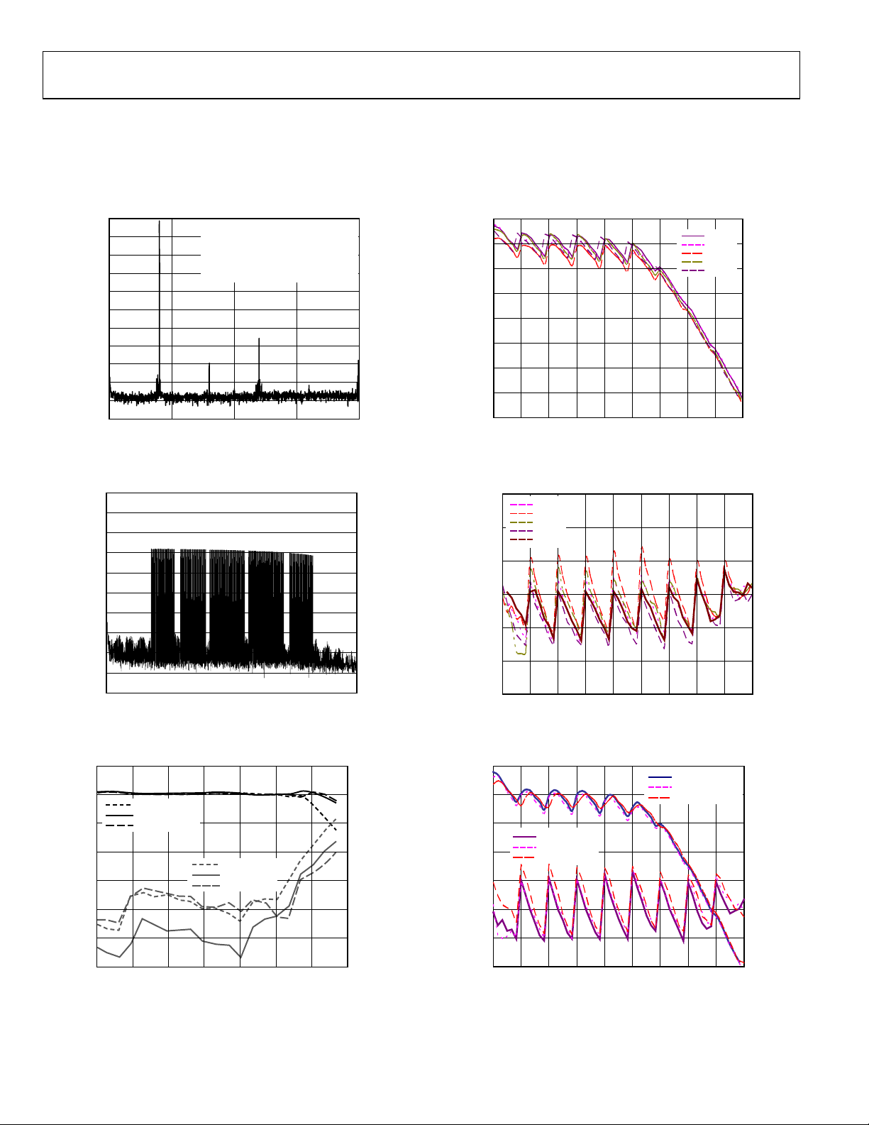
Figure 3. Spectral Plot with 4k FFT of Input Sinusoid
with RxPGA = 0 dB and P
–30
–40
–50
–60
–70
–80
–90
–100
–110
INPUT REFERRED SPECTRUM (dBm)
–120
–130
0 5 10 15 20 25
Figure 4. Spectral Plot with 4k FFT of 84-Carrier DMT Signal
with PAR = 10.2 dB, P
66
SINAD @ 3.14V
60
57
54
SINAD (dBFS)
51
SINAD @ 3.3V
SINAD @ 3.46V
FUND = –1dBFS
SINAD = 61.9dBFS
ENOB = 10BITS
SNR = 64.5dBFS
THD = –65.4dBFS
SFDR = –64.9dBc (THIRD HARMONIC)
RBW = 12.21kHz
FREQUENCY (MHz)
= 9 dBm
IN
RBW = 12.2kHz
FREQUENCY (MHz)
= −33.7 dBm, and RxPGA = 36 dB
IN
THD @ 3.14V
THD @ 3.3V
THD @ 3.46V
OSCIN
= f
= 50 MSPS, low-pass filter’s f
ADC
04560-0-003
04493-0-041
–50
–5663
–62
–68
–74
THD (dBFS)
–80
= 22 MHz, AIN = −1 dBFS,
−3 dB
65
59
56
53
50
SINAD (dBFS)
47
44
41
–6 0 6 12 18 24 30 36 42 48
RxPGA GAIN (dB)
Figure 6. SINAD/ENOB vs. RxPGA Gain and Frequency
–55
–60
–65
–70
THD (dBc)
–75
–80
–85
1MHz
5MHz
10MHz
15MHz
20MHz
–6 0 6 12 18 24 30 36 42 48
RxPGA GAIN (dB)
Figure 7. THD vs. RxPGA Gain and Frequency
65
62
59
56
53
SINAD (dBFS)
50
THD @ +25°C
THD @ +85°C
THD @ –40°C
SINAD @ +25°C
SINAD @ +85°C
SINAD @ –40°C
1MHz
5MHz
10MHz
15MHz
20MHz
10.5
10.062
9.5
9.0
8.5
8.0
7.5
7.0
6.5
–45
–50
–55
–60
–65
–70
ENOB (Bits)
04560-0-006
04560-0-007
THD (dBc)
48
45
–21 –18 –15 –12 –9 –6 –3 0
INPUT AMPLITUDE (dBFS)
(0dBFS = 2V p-p)
Figure 5. SINAD and THD vs. Input Amplitude and Supply
= 8 MHz, LPF f
(f
IN
= 26 MHz; Rx PGA = 0 dB)
−3 dB
–86
04560-0-005
–92
Rev. B | Page 12 of 48
47
44
–6 0 6 12 18 24 30 36 42 48
RxPGA GAIN (dB)
Figure 8. SINAD/THD Performance vs. RxPGA Gain
and Temperature ( f
= 5 MHz)
IN
–75
–80
04560-0-008
AD9866
Rx PATH TYPICAL PERFORMANCE CHARACTERISTICS
AVDD = CLKVDD = DVDD = DRVDD = 3.3 V, f
RIN = 50 Ω, half- or full-duplex interface, default power bias settings.
10
0
–10
–20
–30
–40
–50
–60
–70
–80
REFERRED TO INPUT SPECTRUM (dBm)
–90
–100
0 1020304
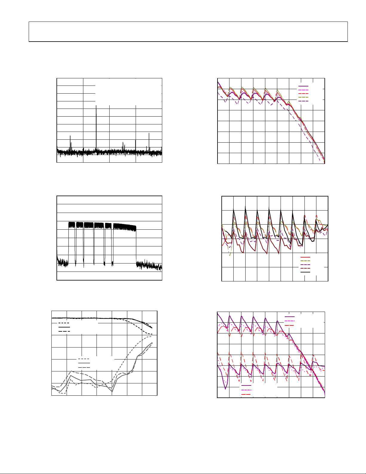
Figure 9. Spectral Plot with 4k FFT of Input Sinusoid
with RxPGA = 0 dB and P
FUND = –1dBFS
SINAD = 62.4dBFS
ENOB = 10.1BITS
SNR = 63.4dBFS
THD = –69.3dBFS
SFDR = –70.5dBc (THIRD HARMONIC)
RBW = 19.53kHz
FREQUENCY (MHz)
= 9 dBm
IN
OSCIN
= f
= 80 MSPS, low-pass filter’s f
ADC
04560-0-009
0
= 30 MHz, AIN = −1 dBFS,
−3 dB
65
62
59
56
53
50
SINAD (dBFS)
47
44
41
–6 0 6 12 18 24 30 36 42 48
RxPGA GAIN (dB)
Figure 12. SINAD/ENOB vs. RxPGA Gain and Frequency
5MHz
10MHz
15MHz
20MHz
30MHz
10.5
10.0
9.5
9.0
8.5
8.0
7.5
7.0
6.5
ENOB (Bits)
04560-0-012
–30
–40
–50
–60
–70
–80
–90
–100
–110
INPUT REFERRED SPECTRUM (dBm)
–120
–130
0 1020304
FREQUENCY (MHz)
RBW = 19.53kHz
Figure 10. Spectral Plot with 4K FFT of 111-Carrier DMT Signal
with PAR = 11 dB, P
66
60
57
54
SINAD (dBFS)
51
48
45
–21 –18 –15 –12 –9 –6 –3 0
= −33.7 dBm, LPF's f
IN
SINAD @ 3.14V
SINAD @ 3.3V
SINAD @ 3.46V
THD @ 3.14V
THD @ 3.3V
THD @ 3.46V
INPUT AMPLITUDE (dBFS)
(0dBFS = 2V p-p)
= 32 MHz and RxPGA = 36 dB
−3 dB
Figure 11. SINAD and THD vs. Input Amplitude and Supply
(f
= 8 MHz, LPF f
IN
= 26 MHz; RxPGA = 0 dB)
−3 dB
04560-0-010
0
–50
–5663
–62
–68
–74
THD (dBFS)
–80
–86
04560-0-011
–92
–55
–60
–65
–70
THD (dBc)
–75
–80
–85
–6 0 6 12 18 24 30 36 42 48
RxPGA GAIN (dB)
5MHz
10MHz
15MHz
20MHz
30MHz
Figure 13. THD vs. RxPGA Gain and Frequency
65
61
59
56
53
50
SINAD (dBFS)
47
44
41
–6 0 6 12 18 24 30 36 42 48
THD @ +25°C
THD @ +85°C
THD @ –40°C
RxPGA GAIN (dB)
SINAD @ +25°C
SINAD @ +85°C
SINAD @ –40°C
–40
–45
–50
–55
–60
–65
–70
–75
–80
Figure 14. SINAD/THD Performance vs. RxPGA Gain and Temperature
= 10 MHz)
(f
IN
04560-0-013
THD (dBc)
04560-0-014
Rev. B | Page 13 of 48
AD9866
65.0
64.5
64.0
63.5
63.0
62.5
62.0
SNR (dBFS)
61.5
61.0
60.5
60.0
0 5 10 15 20 35 30
INPUT FREQUENCY (MHz)
SNR @ 3.14V
SNR @ 3.3V
SNR @ 3.47V
THD @ 3.14V
THD @ 3.3V
THD @ 3.47V
–52
–54
–56
–58
–60
–62
–64
–66
–68
–70
–72
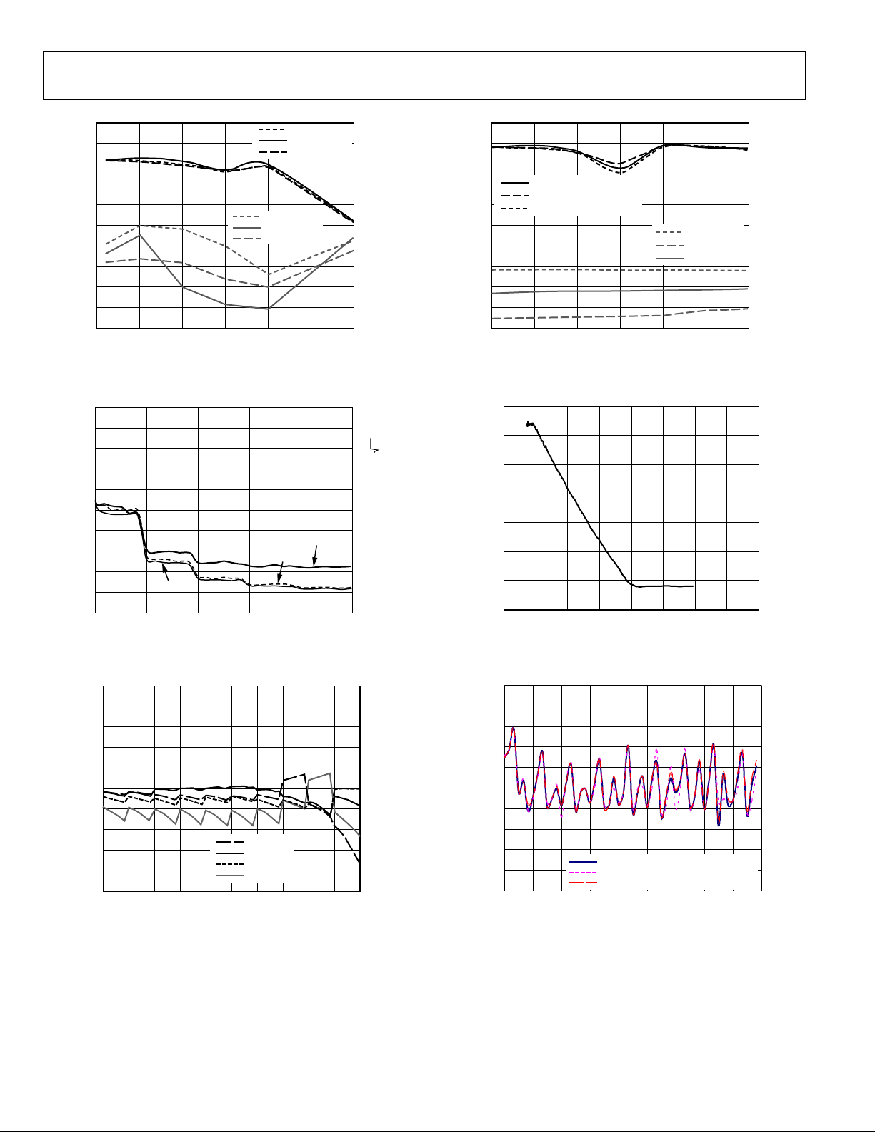
Figure 15. SNR and THD vs. Input Frequency and Supply
( LPF f
109.4
98.5
87.5
76.6
56.6
54.7
43.8
32.8
INTEGRATED NOISE (μV rms)
21.9
10.9
0
18 24 30 36 42 48
= 26 MHz; RxPGA = 0 dB)
−3 dB
+25°C
RxPGA GAIN (dB)
+85°C
–40°C
20
18
16
14
12
10
8
6
4
2
0
Figure 16. Input Referred Integrated Noise and Noise Spectral Density
vs. RxPGA Gain (LPF f
5
4
3
2
1
0
–1
–2
DC OFFSET (% of full scale)
–3
–4
–5
–6 0 6 12 18 24 30 36 42 48
GAIN (dB)
= 26 MHz)
−3 dB
DEVICE 1
DEVICE 2
DEVICE 3
DEVICE 4
04560-0-017
Figure 17. Rx DC Offset vs. RxPGA Gain
THD (dBc)
04560-0-015
NOISE SPECTRAL DENSITY (nV/ Hz)
04560-0-016
63
62
61
60
59
58
57
SNR (dBFS)
56
55
54
53
20 30 40 50 60 70 80
SNR vs. MSPS @ 3.0V
SNR vs. MSPS @ 346V
SNR @ 3.13V
INPUT FREQUENCY (MHz)
SUP
SUP
THD @ 3.13V
THD @ 3.46V
THD @ 3.3V
Figure 18. SNR and THD vs. Sample Rate and Supply
(LPF Disabled; RxPGA = 0 dB; f
45
44
43
42
41
SNR (dB)
40
39
38
0 1020304050607080
CUTOFF FREQUENCY (MHz)
= 8 MHz)
IN
Figure 19. SNR vs. Filter Cutoff Frequency
(50 MSPS; f
0.5
0.4
0.3
0.2
0.1
0
–0.1
–0.2
GAIN STEP ERROR (dB)
–0.3
–0.4
–0.5
–6 0 6 12 18 24 30 36 42 48
Figure 20. RxPGA Gain Step Error vs. Gain (f
= 5 MHz; AIN = −1 dB; RxPGA = 48 dB)
IN
AD9866: GAIN STEP ERROR @ +25°C
AD9866: GAIN STEP ERROR @ +85°C
AD9866: GAIN STEP ERROR @ –40°C
RxPGA GAIN (dB)
= 10 MHz)
IN
–20
–25
–30
–35
–40
–45
–50
–55
–60
–65
–70
THD (dBc)
04560-0-018
04560-0-019
04560-0-020
Rev. B | Page 14 of 48
AD9866
Rx PATH TYPICAL PERFORMANCE CHARACTERISTICS
AVDD = CLKVDD = DVDD = DRVDD = 3.3 V, f
RIN = 50 Ω, half- or full-duplex interface, default power bias settings.
2048
1792
1536
1280
CODE
1024
768
512
256
0 80 160 240 320 400 480 560 640 720
TIME (ns)
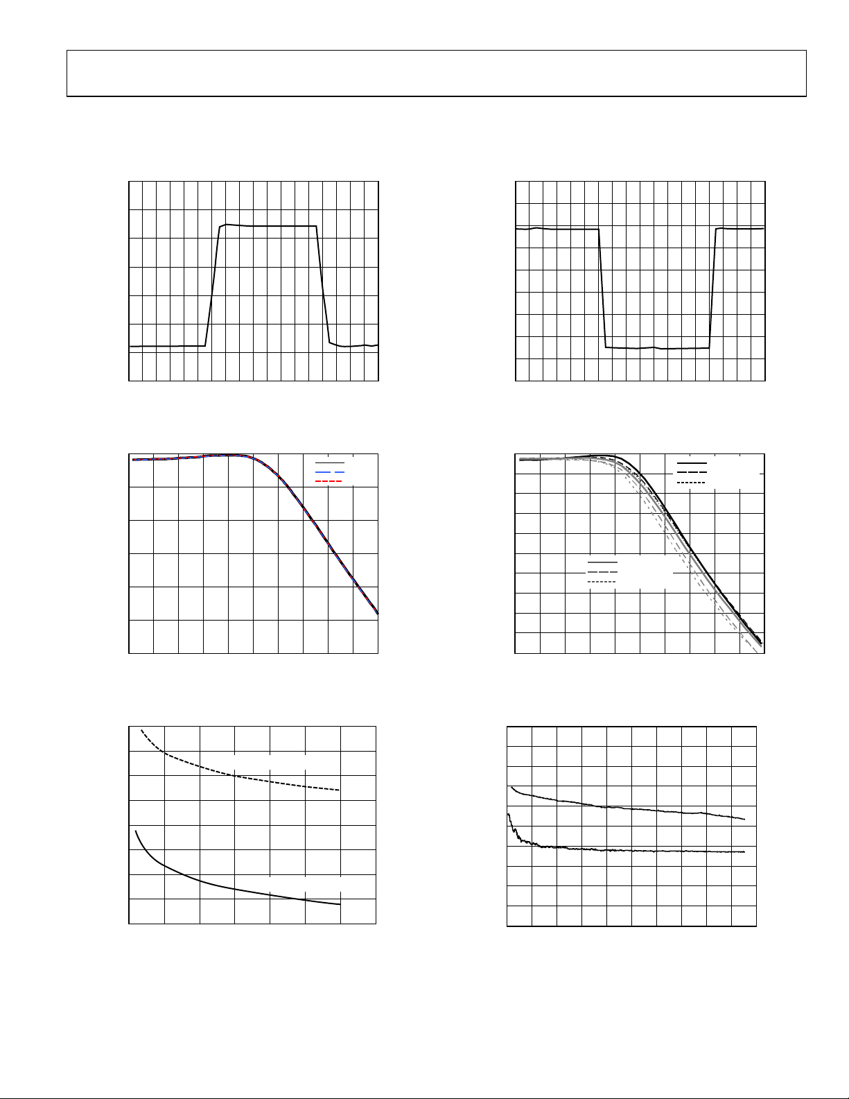
Figure 21. RxPGA Settling Time −12 dB to +48 dB Transition for DC Input
= 50 MSPS, LPF Disabled)
(f
ADC
0
–3
–6
–9
–12
AMPLITUDE RESPONSE (dB)
–15
–18
0 5 10 15 20 25 30 35 40 45 50
INPUT FREQUENCY (MHz)
Figure 22. Rx Low-Pass Filter Amplitude Response vs. Supply
= 50 MSPS, f
(f
ADC
140
130
120
(dB)
110
100
@RxPGA = 0dB
90
ATTEN
80
70
60
0 5 10 15 20 25 30 35
= 33 MHz, RxPGA = 0 dB)
−3 dB
TxDAC ISOLATION @ 0dB
IAMP ISOLATION @ 0dB
FREQUENCY (MHz)
Figure 23. Rx to Tx Full-Duplex Isolation @ 0 RxPGA Setting
(Note: ATTEN
@ RxPGA = x dB
= ATTEN
@ RxPGA = 0 dB
− RxPGA Gain)
OSCIN
3.3V
3.0V
3.6V
= f
= 50 MSPS, low-pass filter disabled, RxPGA = 0 dB, AIN = −1 dBFS,
ADC
1408
1280
1152
1024
896
CODE
768
640
512
384
04560-0-021
256
0 80 160 240 320 400 480 560 640 720
TIME (ns)
Figure 24. RxPGA Settling Time for 0 dB to +5 dB Transition for DC Input
= 50 MSPS, LPF Disabled)
(f
ADC
0
–2
–4
–6
–8
04560-0-022
–10
–12
FUNDAMENTAL (dB)
–14
–16
–18
–20
0 5 10 15 20 25 30 35 40 5045
+18dB GAIN
+30dB GAIN
+42dB GAIN
INPUT FREQUENCY (MHz)
Figure 25. Rx Low-Pass Filter Amplitude Response vs. RxPGA Gain
= 33 MHz)
3 dB
−
IN
C
IN
FREQUENCY (MHz)
04560-0-023
(LPF's f
420
410
400
390
380
370
360
RESISTANCE (Ω)
350
340
330
320
5 105958575655545352515
R
Figure 26. Rx Input Impedance vs. Frequency
–6dB GAIN
0dB GAIN
+6dB GAIN
10
9
8
7
6
5
4
3
2
1
0
04560-0-024
04560-0-025
CAPACITANCE (pF)
04493-0-026
Rev. B | Page 15 of 48
 Loading...