FEATURES
10 MHz to 300 MHz input frequency
6.8 kHz to 270 kHz output signal bandwidth
7.5 dB SSB NF
–7.0 dBm IIP3
AGC free range up to –34 dBm
12 dB continuous AGC range
16 dB front end attenuator
Baseband I/Q 16-bit (or 24-bit) serial digital output
LO and sampling clock synthesizers
Programmable decimation factor, output format,
AGC, and sythesizer settings
370 Ω input impedance
2.7 V to 3.6 V supply voltage
Low current consumption: 17 mA
48-lead LFCSP package
APPLICATIONS
Multimode narrow-band radio products
Analog/digital UHF/VHF FDMA receivers
TETRA, APCO25, GSM/EDGE
Portable and mobile radio products
SATCOM terminals
*Protected by U.S. Patent No. 5,969,657; other patents pending.
PRODUCT OVERVIEW
The AD9864 is a general-purpose IF subsystem that digitizes a
low level 10 MHz to 300 MHz IF input with a signal bandwidth
ranging from 6.8 kHz to 270 kHz. The signal chain of the
AD9864 consists of a low noise amplifier (LNA), a mixer, a
band-pass Σ-∆ analog-to-digital converter (ADC), and a decimation filter with programmable decimation factor. An automatic gain control (AGC) circuit gives the AD9864 12 dB of
continuous gain adjustment. Auxiliary blocks include both
clock and LO synthesizers.
The high dynamic range of the AD9864 and inherent antialiasing provided by the band-pass Σ-∆ converter allow the device to
cope with blocking signals up to 95 dB stronger than the desired
signal. This attribute often reduces the cost of a radio by reducing IF filtering requirements. Also, it enables multimode radios
of varying channel bandwidths, allowing the IF filter to be
specified for the largest channel bandwidth.
The SPI® port programs numerous parameters of the AD9864,
allowing the device to be optimized for any given application.
Programmable parameters include synthesizer divide ratios,
AGC attenuation and attack/decay time, received signal
strength level, decimation factor, output data format, 16 dB
attenuator, and the selected bias currents.
The AD9864 is available in a 48-lead LFCSP package and
operates from a single 2.7 V to 3.6 V supply. The total power
consumption is typically 56 mW and a power-down mode is
IF Digitizing Subsystem
AD9864*
provided via serial interfacing.
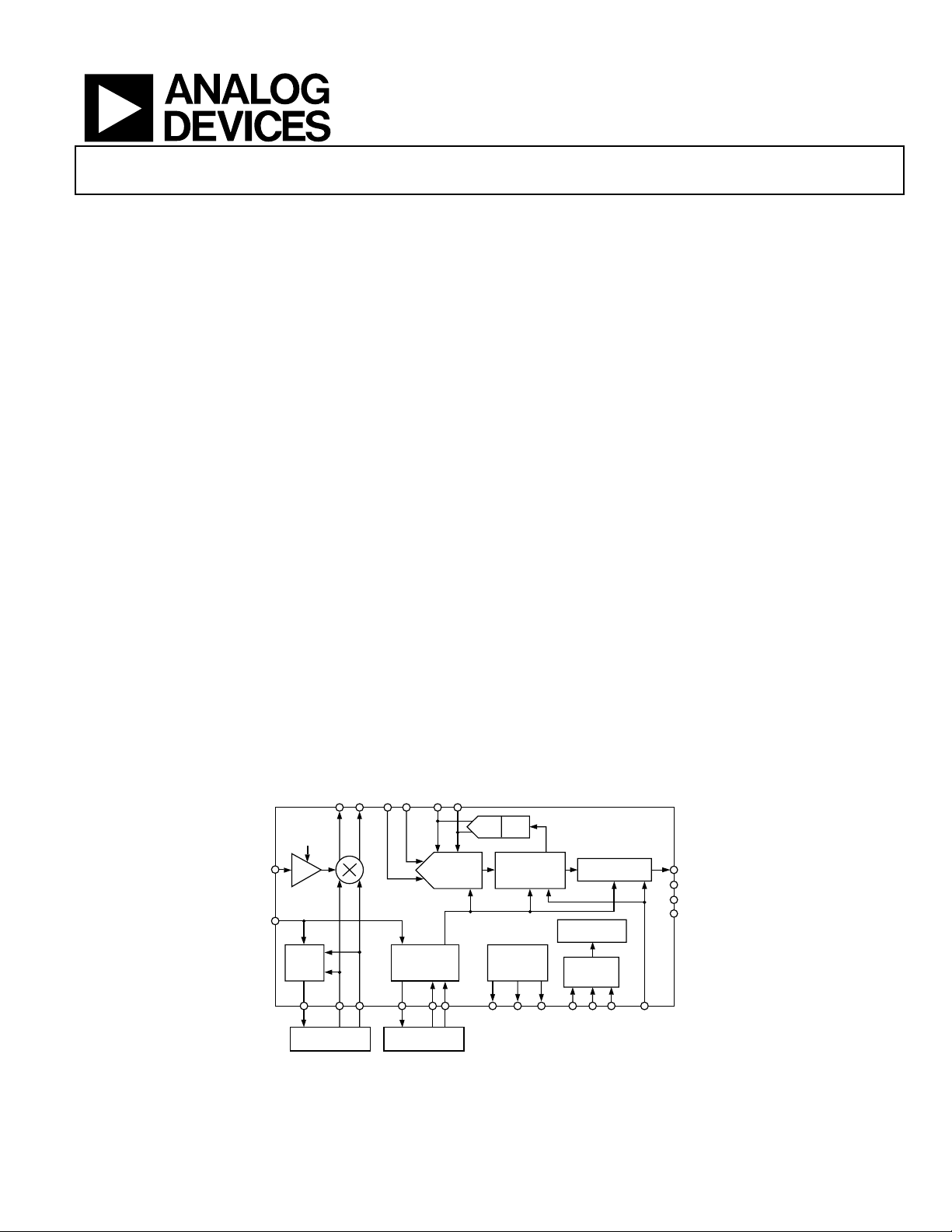
FUNCTIONAL BLOCK DIAGRAM
MXOP MXON IF2P IF2N GCP GCN
–16dB
LNA
IFIN
FREF
LO
SYN
LO VCO AND
LOOP FILTER
Rev. 0
Information furnished by Analog Devices is believed to be accurate and reliable.
However, no responsibility is assumed by Analog Devices for its use, nor for any
infringements of patents or other rights of third parties that may result from its use.
Specifications subject to change without notice. No license is granted by implication
or otherwise under any patent or patent rights of Analog Devices. Trademarks and
registered trademarks are the property of their respective companies.
∑-∆ ADC
CLK SYN
CLKNCLKPIOUTCLONLOPIOUTL
LOOP FILTER
Figure 1. AD9864 Block Diagram
DAC AGC
DECIMATION
FILTER
VOLTAGE
REFERENCE
One Technology Way, P.O. Box 9106, Norwood, MA 02062-9106, U.S.A.
Tel: 781.329.4700 www.analog.com
Fax: 781.326.8703 © 2003 Analog Devices, Inc. All rights reserved.
AD9864
FORMATTING/SSI
CONTROL LOGIC
SPI
DOUTA
DOUTB
FS
CLKOUT
SYNCBPEPDPCVREFNVCMVREFP
04319-0-001

AD9864
TABLE OF CONTENTS
General Description ......................................................................... 3
IF LNA/Mixer............................................................................. 26
AD9864 Specifications..................................................................... 4
Digital Specifications........................................................................ 6
Absolute Maximum Ratings............................................................ 7
Thermal Resistance ...................................................................... 7
Pin Configuration and Functional Descriptions.......................... 8
Definition of Specifications/Test Methods ............................... 9
Typical Performance Characteristics ........................................... 10
Serial Peripheral Interface (SPI)............................................... 15
Theory of Operation ...................................................................... 17
Serial Port Interface (SPI).......................................................... 17
Synchronous Serial Interface (SSI)........................................... 18
Syncronization Using SYNCB ..................................................22
Interfacing to DSPs..................................................................... 22
Power Control............................................................................. 23
LO Synthesizer............................................................................ 23
Fast Acquire Mode...................................................................... 24
Band-Pass ∑-∆ ADC .................................................................. 27
Decimation Filter ....................................................................... 29
Variable Gain Amplifier Operation With Automatic Gain
Control......................................................................................... 30
Variable Gain Control................................................................ 31
Automatic Gain Control (AGC)............................................... 32
System Noise Figure (NF) Versus VGA (or AGC) Control .. 34
Applications Considerations..................................................... 35
Spurious Responses.................................................................... 37
External Passive Component Requirements .......................... 37
Applications ................................................................................ 38
Layout Example, Evaluation Board, and Software ................. 42
Outline Dimensions....................................................................... 43
ESD Caution................................................................................ 43
Ordering Guide .......................................................................... 43
Clock Synthesizer ....................................................................... 24
REVISION HISTORY
Revision 0: Initial Version
Rev. 0 | Page 2 of 44

AD9864
GENERAL DESCRIPTION
The AD9864 is a general-purpose narrow-band IF subsystem that
digitizes a low level 10 MHz to 300 MHz IF input with a signal
bandwidth ranging from 6.8 kHz to 270 kHz. The signal chain of
the AD9864 consists of an LNA, a mixer, a band-pass Σ-∆ ADC,
and a decimation filter with programmable decimation factor.
The input LNA is a fixed gain block with an input impedance of
approximately 370 Ω||1.4 pF. The LNA input is single-ended
and self-biasing, allowing the input IF to be ac-coupled. The
LNA can be disabled through the serial interface, providing a
fixed 16 dB attenuation to the input signal.
The LNA drives the input port of a Gilbert-type active mixer.
The mixer LO port is driven by the on-chip LO buffer, which
can be driven externally, single-ended or differential. The LO
buffer inputs are self-biasing and allow the LO input to be
ac-coupled. The open-collector outputs of the mixer drive an
external resonant tank consisting of a differential LC network
tuned to the IF of the band-pass Σ-∆ ADC.
The external differential LC tank forms the resonator for the
first stage of the band-pass Σ-∆ ADC. The tank LC values must
be selected for a center frequency of f
sample rate of the ADC. The f
/8 frequency is the IF digitized
CLK
/8, where f
CLK
CLK
is the
by the band-pass Σ-∆ ADC. On-chip calibration allows standard tolerance inductor and capacitor values. The calibration is
typically performed once at power-up.
The ADC contains a sixth order multibit band-pass Σ-∆ modulator that achieves very high instantaneous dynamic range over
a narrow frequency band centered at f
/8. The modulator
CLK
output is quadrature mixed to baseband and filtered by three
cascaded linear phase FIR filters to remove out-of-band noise.
The first FIR filter is a fixed decimate by 12 using a fourth order
comb filter. The second FIR filter also uses a fourth order comb
filter with programmable decimation from 1 to 16. The third
FIR stage is programmable for decimation of either 4 or 5. The
cascaded decimation factor is programmable from 48 to 960.
The decimation filter data is output via the synchronous serial
interface (SSI) of the chip.
Additional functionality built into the AD9864 includes LO and
clock synthesizers, programmable AGC, and a flexible synchronous serial interface for output data.
The LO synthesizer is a programmable PLL consisting of a low
noise phase frequency detector (PFD), a variable output current
charge pump (CP), a 14-bit reference divider, A and B counters,
and a dual modulus prescaler. The user only needs to add an
appropriate loop filter and VCO for complete operation.
The clock synthesizer is equivalent to the LO synthesizer with
the following differences:
• It does not include the prescaler or A counter.
• It includes a negative resistance core used for VCO
generation.
The AD9864 contains both a variable gain amplifier (VGA) and a
digital VGA (DVGA). Both of these can operate manually or
automatically. In manual mode, the gain for each is programmed
through the SPI. In automatic gain control mode, the gains are
adjusted automatically to ensure the ADC does not clip and that
the rms output level of the ADC is equal to a programmable reference level.
The VGA has 12 dB of attenuation range and is implemented by
adjusting the ADC full-scale reference level. The DVGA gain is
implemented by scaling the output of the decimation filter. The
DVGA is most useful in extending the dynamic range in narrow-band applications requiring 16-bit I and Q data format.
The SSI provides a programmable frame structure, allowing
24-bit or 16-bit I and Q data and flexibility by including
attenuation and RSSI data if required.
Rev. 0 | Page 3 of 44

AD9864
AD9864 SPECIFICATIONS
Table 1. VDDI = VDDF = VDDA = VDDC = VDDL = VDDH = 2.7 V to 3.6 V, VDDQ = VDDP = 2.7 V to 5.5 V, f
= 109.65 MHz, fLO = 107.4 MHz, f
f
IF
= 16.8 MHz, unless otherwise noted. Standard operating mode: VGA at minimum attenuation
REF
setting, synthesizers in normal (not fast acquire) mode, decimation factor = 900, 16-bit digital output, and 10 pF load on SSI output pins.
Parameter Temperature Test Level Min Typ Max Unit
SYSTEM DYNAMIC PERFORMANCE1
SSB Noise Figure @ Minimum VGA Attenuation
@ Maximum VGA Attenuation
Dynamic Range with AGC Enabled
2,3
Full IV 13 dB
2,3
Full IV 91 95 dB
2, 3
Full IV 7.5 9.5 dB
IF Input Clip Point @ Maximum VGA Attenuation3 Full IV –20 –19 dBm
@ Minimum VGA Attenuation3 Full IV –32 –31 dBm
Input Third Order Intercept (IIP3) Full IV –12 –7.0 dBm
Gain Variation over Temperature Full IV 0.7 2 dB
LNA + MIXER
Maximum RF and LO Frequency Range Full IV 300 500 MHz
LNA Input Impedance 25°C V
Mixer LO Input Resistance 25°C V
370||1.4
1
LO SYNTHESIZER
LO Input Frequency Full IV 7.75 300 MHz
LO Input Amplitude Full IV 0.3 2.0 V p-p
FREF Frequency (for Sinusoidal Input Only) Full IV 8 25 MHz
FREF Input Amplitude Full IV 0.3 3 V p-p
FREF Slew Rate Full IV 7.5 V/µs
Minimum Charge Pump Current @ 5 V4 Full VI 0.67 mA
Maximum Charge Pump Current @ 5 V4 Full VI 5.3 mA
Charge Pump Output Compliance5 Full VI 0.4 VDDP – 0.4 V
Synthesizer Resolution Full IV 6.25 kHz
CLOCK SYNTHESIZER
CLK Input Frequency Full IV 13 26 MHz
CLK Input Amplitude Full IV 0.3 VDDC V p-p
Minimum Charge Pump Output Current4 Full VI 0.67 mA
Maximum Charge Pump Output Current4 Full VI 5.3 mA
Charge Pump Output Compliance5 Full VI 0.4 VDDQ – 0.4 V
Synthesizer Resolution Full VI 2.2 kHz
Σ-∆ ADC
Resolution Full IV 16 24 Bits
Clock Frequency (f
Center Frequency Full V f
) Full IV 13 26 MHz
CLK
/8 MHz
CLK
Pass-Band Gain Variation Full IV 1.0 dB
Alias Attenuation Full IV 80 dB
GAIN CONTROL
Programmable Gain Step Full V 16 dB
AGC Gain Range Full V 12 dB
GCP Output Resistance Full IV
50 72.5
= 18 MSPS,
CLK
95
Ω||pF
kΩ
kΩ
1
This includes 0.9 dB loss of matching network.
2
AGC with DVGA enabled.
3
Measured in 10 kHz bandwidth.
4
Programmable in 0.67 mA steps.
5
Voltage span in which LO (or CLK) charge pump output current is maintained within 5% of nominal value of VDDP/2 (or VDDQ/2).
Rev. 0 | Page 4 of 44
AD9864
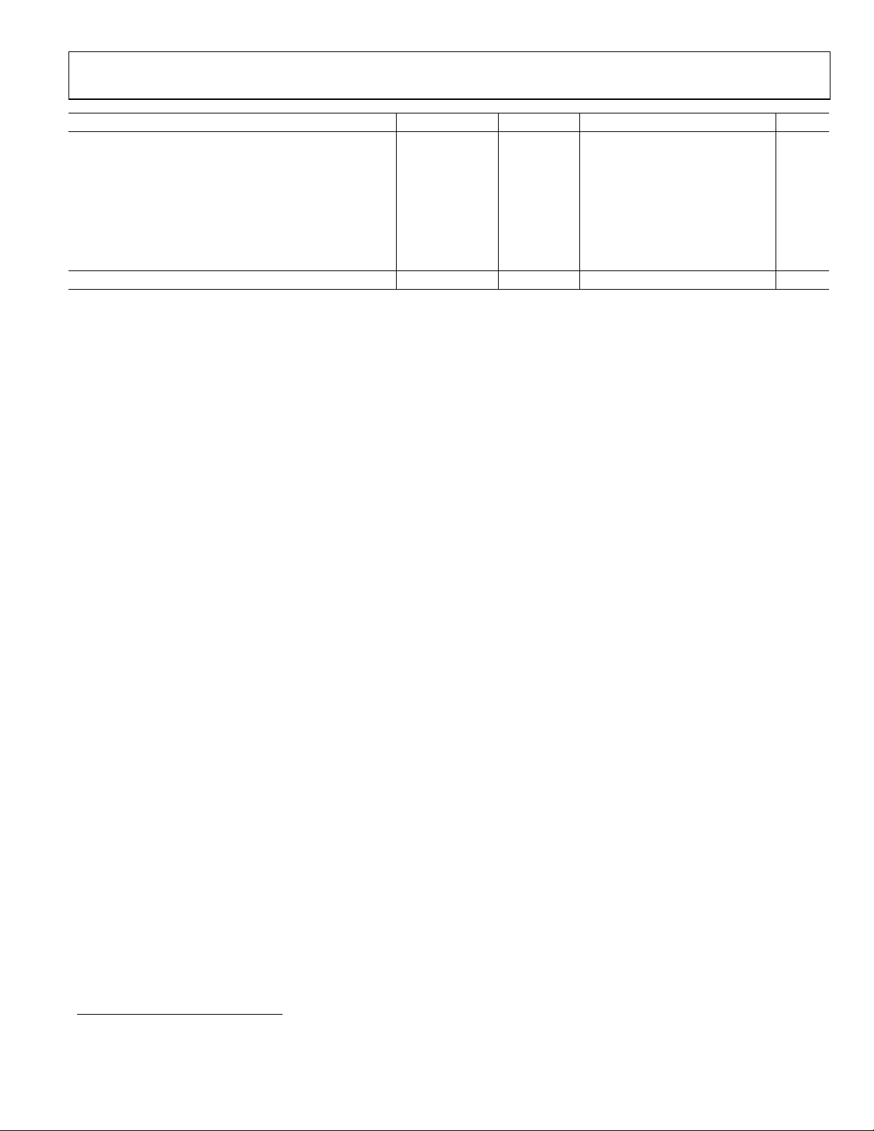
Parameter Temperature Test Level Min Typ Max Unit
OVERALL
Analog Supply Voltage (VDDA, VDDF, VDDI) Full VI 2.7 3.0 3.6 V
Digital Supply Voltage (VDDD, VDDC, VDDL) Full VI 2.7 3.0 3.6 V
Interface Supply Voltage (VDDH)1 Full VI 1.8 3.6 V
Charge Pump Supply Voltage (VDDP, VDDQ) Full VI 2.7 5.0 5.5 V
Total Current
Operation Mode2 Full VI 17 mA
Standby Full VI 0.01 mA
OPERATING TEMPERATURE RANGE –40 +85 °C
1
VDDH must be less than VDDD + 0.5 V.
2
Clock VCO off and additional 0.7 mA with VGA @ maximum attenuation.
Rev. 0 | Page 5 of 44

AD9864
DIGITAL SPECIFICATIONS
Table 2. VDDI = VDDF = VDDA = VDDC = VDDL = VDDH = 2.7 V to 3.6 V, VDDQ = VDDP = 2.7 V to 5.5 V, f
= 109.65 MHz, fLO = 107.4 MHz, f
f
IF
= 16.8 MHz, unless otherwise noted. Standard operating mode: VGA at minimum attenuation
REF
setting, synthesizers in normal (not fast acquire) mode, decimation factor = 900, 16-bit digital output, and 10 pF load on SSI output pins.
Parameter Temperature Test Level Min Typ Max Unit
DECIMATOR
Decimation Factor1 Full IV 48 960
Pass-Band Width Full V 50% f
Pass-Band Gain Variation Full IV 1.2 dB
Alias Attenuation Full IV 88 dBm
SPI-READ OPERATION (See Figure 30)
PC Clock Frequency Full IV 10 MHz
PC Clock Period (t
) Full IV 100 ns
CLK
PC Clock High (tHI) Full IV 45 ns
PC Clock Low (t
) Full IV 45 ns
LOW
PC to PD Setup Time (tDS) Full IV 2 ns
PC to PD Hold Time (tDH) Full IV 2 ns
PE to PC Setup Time (tS) Full IV 5 ns
PC to PE Hold Time (tH) Full IV 5 ns
SPI-WRITE OPERATION2 (See Figure 29)
PC Clock Frequency Full IV 10 MHz
PC Clock Period (t
) Full IV 100 ns
CLK
PC Clock High (tHI) Full IV 45 ns
PC Clock Low (t
) Full IV 45 ns
LOW
PC to PD Setup Time (tDS) Full IV 2 ns
PC to PD Hold Time (tDH) Full IV 2 ns
PC to PD (or DOUTB) Data Valid Time (tDV) Full IV 3 ns
PE to PD Output Valid to Hi-Z (tEZ) Full IV 8 ns
SSI2 (See Figure 32)
CLKOUT Frequency Full IV 0.867 26 MHz
CLKOUT Period (t
CLKOUT Duty Cycle (tHI, t
) Full IV 38.4 1153 ns
CLK
) Full IV 33 50 67 ns
LOW
CLKOUT to FS Valid Time (tV) Full IV –1 +1 ns
CLKOUT to DOUT Data Valid Time (tDV) Full IV –1 +1 ns
CMOS LOGIC INPUTS3
Logic 1 Voltage (VIH) Full IV VDDH – 0.2 V
Logic 0 Voltage (VIL) Full IV 0.5 V
Logic 1 Current (IIH) Full IV 10 µA
Logic 0 Current (IIL) Full IV 10 µA
Input Capacitance Full IV 3 pF
CMOS LOGIC OUTPUTS
2, 3, 4
Logic 1 Voltage (VOH) Full IV VDDH – 0.2 V
Logic 0 Voltage (VOL) Full IV 0.2 V
= 18 MSPS,
CLK
CLKOUT
1
Programmable in steps of 48 or 60.
2
CMOS output mode with C
3
Absolute maximum and minimum input/output levels are VDDH + 0.3 V and –0.3 V.
4
IOL = 1 mA; specification is also dependent on drive strength setting.
= 10 pF and Drive Strength = 7.
LOAD
Rev. 0 | Page 6 of 44
AD9864
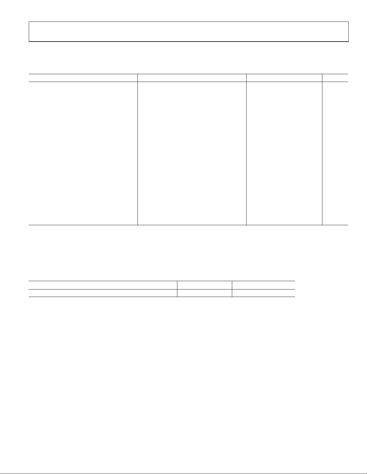
ABSOLUTE MAXIMUM RATINGS
Table 3. AD9864 Absolute Maximum Ratings
Parameter With Respect to Min Max Unit
VDDF, VDDA, VDDC,
VDDD, VDDH, VDDL, VDDI
VDDF, VDDA, VDDC,
VDDD, VDDH, VDDL, VDDI
VDDP, VDDQ GNDP, GNDQ –0.3 +6.0 V
GNDF, GNDA, GNDC, GNDD,
GNDH, GNDL, GNDI, GNDQ, GNDP, GNDS
MXOP, MXON, LOP,
LON, IFIN, CXIF, CXVL, CXVM
PC, PD, PE, CLKOUT,
DOUTA, DOUTB, FS, SYNCB
IF2N, IF2P, GCP, GCN GNDF –0.3 VDDF + 0.3 V
VFEFP, VREGN, RREF GNDA –0.3 VDDA + 0.3 V
IOUTC GNDQ –0.3 VDDQ + 0.3 V
IOUTL GNDP –0.3 VDDP + 0.3 V
CLKP, CLKN GNDC –0.3 VDDC + 0.3 V
FREF GNDL –0.3 VDDL + 0.3 V
Junction Temperature 150 °C
Storage Temperature –65 +150 °C
Lead Temperature 300 °C
GNDF, GNDA, GNDC, GNDD,
GNDH, GNDL, GNDI, GNDS
VDDR, VDDA, VDDC,
VDDD, VDDH, VDDL, VDDI
GNDF, GNDA, GNDC, GNDD,
GNDH, GNDL, GNDI, GNDQ, GNDP, GNDS
GNDH –0.3 VDDI + 0.3 V
GNDH –0.3 VDDH + 0.3 V
–0.3 +4.0 V
–4.0 +4.0 V
–0.3 +0.3 V
Stresses above those listed under Absolute Maximum Ratings may cause permanent damage to the device. This is a stress rating only;
functional operation of the device at these or any other conditions above those indicated in the operational section of this specification is
not implied. Exposure to absolute maximum rating conditions for extended periods may affect device reliability.
THERMAL RESISTANCE
θJA is specified for the worst-case conditions, i.e., θJA is specified for device soldered in circuit board for surface-mount packages.
Table 4. Thermal Resistance
Package Type
48-Lead LFCSP 29.5 °C/W
θ
JA
Unit
Rev. 0 | Page 7 of 44
AD9864
V
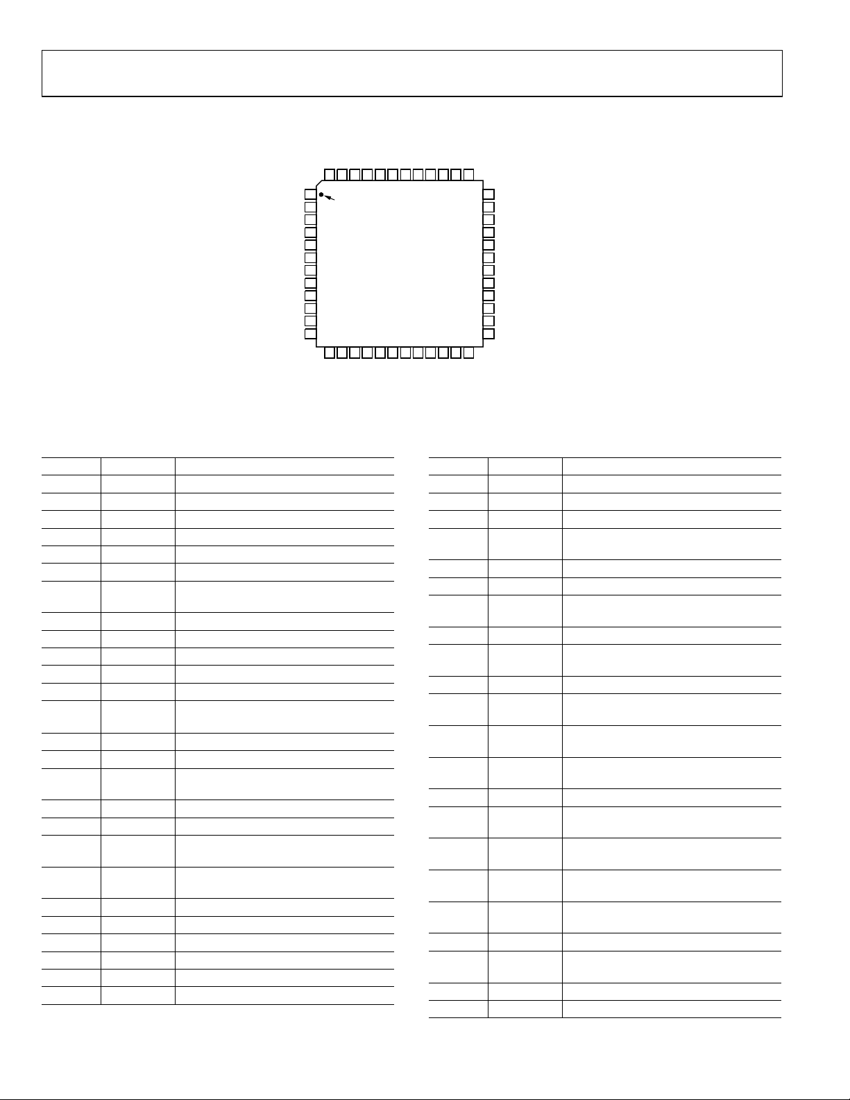
PIN CONFIGURATION AND FUNCTIONAL DESCRIPTIONS
MXOP
MXON
GNDF
IF2N
IF2P
VDDF
GCP
GCN
VDDA
GNDA
VREFP
REFN
VDDIRREF
CXIFIOUTC
IFINVDDQ
48
45
46
47
1
PIN 1
2
IDENTIFIER
3
4
5
6
7
8
9
10
11
12
13
16
15
14
LOPGNDC
CXVLVDDC
GNDIGNDQ
421943
44
AD9864
TOP VIEW
(Not to Scale)
18
17
LONCLKP
41
20
CXVMCLKN
VDDLGNDS
402139
VDDPGNDD
22
IOUTLPC
GNDPPD
38
37
36
35
34
33
32
31
30
29
28
27
26
25
23
24
Figure 2. 48-Lead LFCSP, Backside Paddle Contact Is Connected to Ground
Table 5. Pin Function Descriptions—48-Lead Lead Frame Chip Scale Package (LFCSP)
Pin No. Mnemonic Description
1 MXOP Mixer Output, Positive
2 MXON Mixer Output, Negative
3 GNDF Ground for Front End of ADC
4 IF2N Second IF Input (to ADC), Negative
Pin No. Mnemonic Description
27 VDDH Positive Supply for Digital Interface
28 CLKOUT Clock Output for SSI Port
29 DOUTA Data Output for SSI Port
30 DOUTB
5 IF2P Second IF Input (to ADC), Positive
6 VDDF Positive Supply for Front End of ADC
7 GCP
Filter Capacitor for ADC Full-Scale
Control
31 FS Frame Sync for SSI Port
32 GNDH Ground for Digital Interface
33 SYNCB
8 GCN Full-Scale Control Ground
9 VDDA Positive Supply for ADC Back End
10 GNDA Ground for ADC Back End
11 VREFP Voltage Reference, Positive
12 VREFN Voltage Reference, Negative
13 RREF
Reference Resistor: Requires 100 kΩ to
GNDA
14 VDDQ Positive Supply for Clock Synthesizer
15 IOUTC Clock Synth Charge Pump Out Current
16 GNDQ
Ground for Clock Synthesizer Charge
Pump
17 VDDC Positive Supply for Clock Synthesizer
34 GNDS Substrate Ground
35 FREF
36 GNDL Ground for LO Synthesizer
37 GNDP
38 IOUTL
39 VDDP
40 VDDL Postive Supply for LO Synthesizer
41 CXVM
18 GNDC Ground for Clock Synthesizer
19 CLKP
Sampling Clock Input/Clock VCO Tank,
42 LON
Positive
20 CLKN
Sampling Clock Input/Clock VCO Tank,
43 LOP
Negative
21 GNDS Substrate Ground
44 CXVL
22 GNDD Ground for Digital Functions
23 PC Clock Input for SPI Port
24 PD Data I/O for SPI Port
45 GNDI Ground for Mixer and LNA
46 CXIF
25 PE Enable Input for SPI Port
26 VDDD Positive Supply for Internal Digital
47 IFIN First IF Input (to LNA)
48 VDDI Positive Supply for LNA and Mixer
GNDL
FREF
GNDS
SYNCB
GNDH
FS
DOUTB
DOUTA
CLKOUT
VDDH
VDDD
PE
04319-0-002
Data Output for SSI Port (Inverted) or
SPI Port
Resets SSI and DecimatorCounters;
Active Low
Reference Frequency Input for Both
Synthesizers
Ground for LO Synthesizer Charge
Pump
LO Synthesizer Charge Pump Out
Current
Positive Supply for LO Synthesizer
Charge Pump
External Filter Capacitor; DC Output of
LNA
LO Input to Mixer and LO Synthesizer,
Negative
LO Input to Mixer and LO Synthesizer,
Positive
External Bypass Capacitor for LNA
Power Supply
External Capacitor for Mixer V-I
Converter Bias
Rev. 0 | Page 8 of 44

AD9864
(
)
(
)
=
DEFINITION OF SPECIFICATIONS/TEST METHODS
Single Sideband Noise Figure (SSB NF)
Noise figure (NF) is defined as the degradation in SNR performance (in dB) of an IF input signal after it passes through a
component or system. It can be expressed with the equation
SNRSNRFigureNoise /log10 ×=
IN
OUT
The term SSB is applicable for heterodyne systems containing a
mixer. It indicates that the desired signal spectrum resides on
only one side of the LO frequency (i.e., single sideband); thus a
“noiseless” mixer has a noise figure of 3 dB.
The SSB noise figure of the AD9864 is determined by the equation
SNR)BWPNFSSB
–dBm/Hz174(–log10– −×=
where P
[]
IN
is the input power of an unmodulated carrier, BW is
IN
the noise measurement bandwidth, –174 dBm/Hz is the thermal noise floor at 293K, and SNR is the measured signal-tonoise ratio in dB of the AD9864.
Note that P
is set to –85 dBm to minimize any degradation in
IN
measured SNR due to phase noise from the RF and LO signal
generators. The IF frequency, CLK frequency, and decimation
factors are selected to minimize any spurious components
falling within the measurement bandwidth. Note also that a
bandwidth of 10 kHz is used for the data sheet specification. All
references to noise figures within this data sheet imply single
sideband noise figure.
Input Third Order Intercept (IIP3)
IIP3 is a figure of merit used to determine a component’s or
system’s susceptibility to intermodulation distortion (IMD)
from its third order nonlinearities. Two unmodulated carriers
at a specified frequency relationship (f1 and f2) are injected into
a nonlinear system exhibiting third order nonlinearities producing IMD components at 2f1 – f2 and 2f2 – f1. IIP3 graphically represents the extrapolated intersection of the carrier’s
input power with the third order IMD component when plotted in dB. The difference in power (D in dBc) between the two
carriers and the resulting third order IMD components can be
determined from the equation
Dynamic Range (DR)
Dynamic range is the measure of a small target input signal
(P
) in the presence of a large unwanted interferer signal
TARGET
). Typically, the large signal will cause some unwanted
(P
INTER
characteristic of the component or system to degrade, thus making it unable to detect the smaller target signal correctly. In the
case of the AD9864, it is often a degradation in noise figure at
increased VGA attenuation settings that limits its dynamic range.
The test method for the AD9864 is as follows. The small target
signal (an unmodulated carrier) is input at the center of the IF
frequency, and its power level (P
SNR
of 6 dB. The power of the signal is then increased by
TARGET
) is adjusted to achieve an
TARGET
3 dB prior to injecting the interferer signal. The offset frequency
of the interferer signal is selected so that aliases produced by the
decimation filter’s response as well as phase noise from the LO
(due to reciprocal mixing) do not fall back within the measurement bandwidth. For this reason, an offset of 110 kHz was
selected. The interferer signal (also an unmodulated carrier) is
then injected into the input and its power level is increased to the
point (P
) where the target signal SNR is reduced to 6 dB. The
INTER
dynamic range is determined with the equation
–
SNRPPDR +
TARGETTARGETINTER
Note that the AD9864’s AGC is enabled for this test.
IF Input Clip Point
The IF input clip point is defined as the input power that
results in a digital output level 2 dB below full-scale. Unlike
other linear components that typically exhibit a soft compression (characterized by its 1 dB compression point), an ADC
exhibits a hard compression once its input signal exceeds its
rated maximum input signal range. In the case of the AD9864,
which contains a Σ-∆ ADC, hard compression should be
avoided because it causes severe SNR degradation.
()
PIIPD –32 ×=
IN
Rev. 0 | Page 9 of 44
AD9864
TYPICAL PERFORMANCE CHARACTERISTICS
9.5
0
9.0
8.5
8.0
7.5
NF (dB)
7.0
6.5
6.0
2.7 3.0 3.3 3.6
+85°C
+25°C
–40°C
VDDx (V)
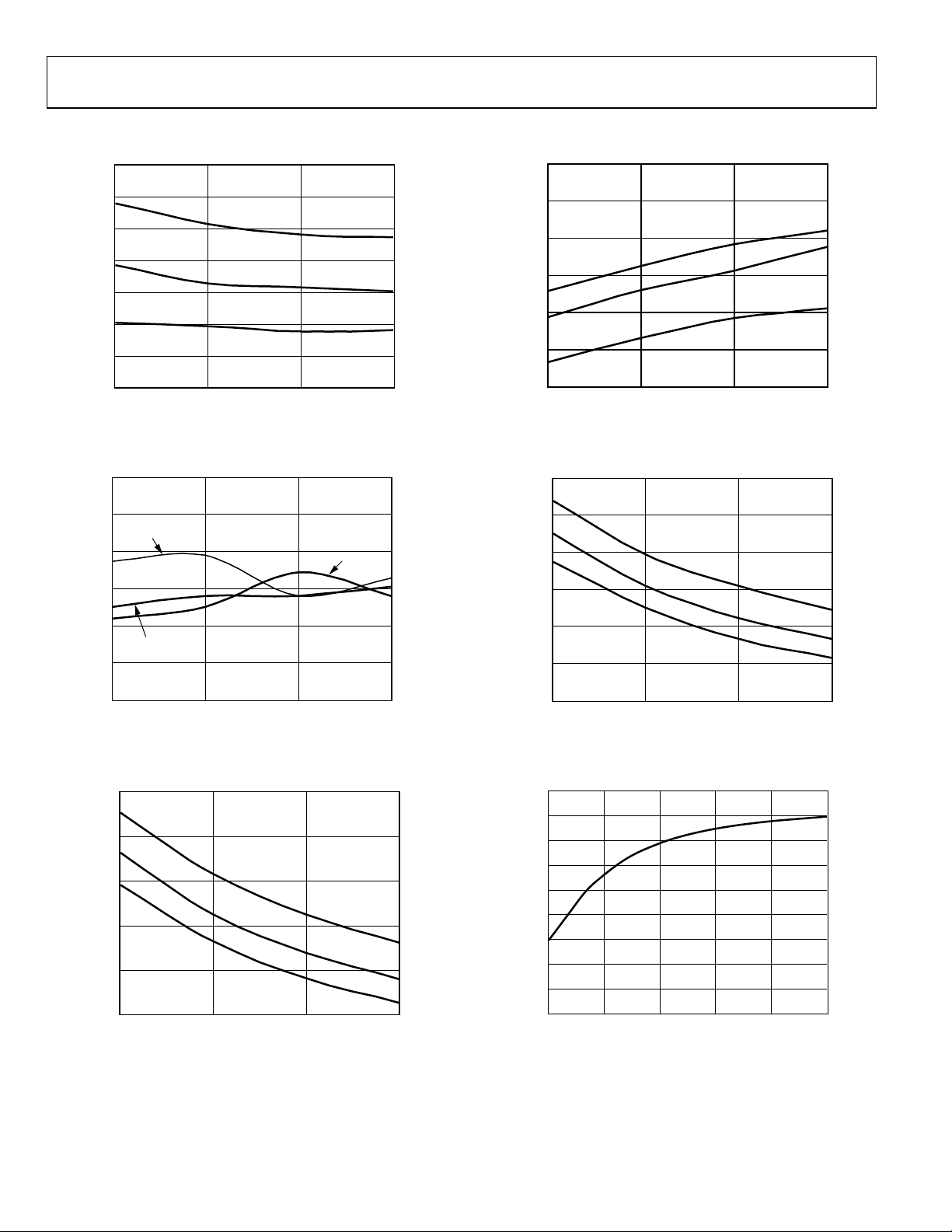
Figure 3. SSB Noise Figure vs. Supply
98
97
+25°C
96
95
DR (dB)
94
93
+85°C
–40°C
04319-0-003
IIP3 (dBm)
INPUT CLIP POINT (dBm)
–2
–4
–6
–8
–10
–12
–17.5
–18.0
–18.5
–19.0
–19.5
–20.0
2.7
+85°C
+25°C
–40°C
3.0 3.3 3.6
VDDx (V)
Figure 6. IIP3 vs. Sup ply
+85°C
+25°C
–40°C
04319-0-004
92
2.7
3.0 3.3 3.6
VDDx (V)
Figure 4. Dynamic Range vs. Supply
–29.5
–30.0
–30.5
–31.0
INPUT CLIP POINT (dBm)
–31.5
–32.0
2.7
3.0 3.3 3.6
VDDx (V)
Figure 5. Minimum VGA Attenuation Clip Point vs. Supply
+85°C
+25°C
–40°C
04319-0-005
04319-0-007
–20.5
2.7
3.0 3.3 3.6
VDDx (V)
Figure 7. Maximum VGA Attenuation Clip Point vs. Supply
0.1
0
–0.1
–0.2
–0.3
–0.4
–0.5
GAIN VARIATION (dB)
–0.6
–0.7
–0.8
–20
–14 –8 –5
LO DRIVE (dBm)
–11–17
Figure 8. Normalized Gain Variation vs. LO Drive (VDDx = 3.0 V)
04319-0-006
04319-0-008
Rev. 0 | Page 10 of 44

AD9864
9.0
8.8
8.6
8.4
8.2
8.0
7.8
NOISE FIGURE (dBc)
7.6
7.4
7.2
7.0
–20
NF
IMD
–10 0 5
LO DRIVE (dBm)
–5–15
Figure 9. Noise Figure and IMD vs. LO Drive (VDDx = 3.0 V )
0
–10
–20
–30
–40
–50
–60
–70
–80
IMD WITH IFIN = –36 dBm (dBc)
–12
–15
–18
–21
–24
dBm
–27
–30
–33
–36
04319-0-009
–36 –33 –30 –27 –24 –21 –18 –15 –12 –9 –6 –3 –0
IFIN (dBm)
04319-0-010
Figure 12. Gain Compression vs. IFIN with 16 dB LNA Attenuator Enabled
dBFS
–10
–12
–14
0
–2
–4
–6
–8
–30
ADC DOES NOT GO INTO
HARD COMPRESSION
3.6V
3.3V
3.0V
2.7V
–28 –26 –24 –22 –20 –18 –14
IFIN (dBm)
Figure 10. Gain Compression vs. IFIN
10.0
NOISE FIGURE (dB)
9.5
9.0
8.5
8.0
7.5
10
I/Q DATA
24-BIT
I/Q DATA
16-BIT
CHANNEL BANDWIDTH (kHz)
16-BIT
I/Q DATA WITH
DVGA ENABLED
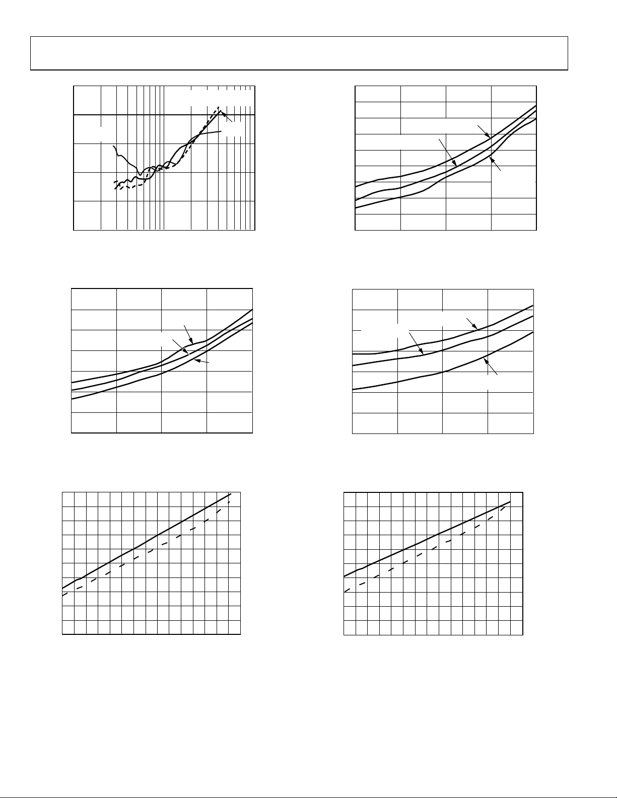
Figure 11. Noise Figure vs. BW (Minimum Attenuation, f
–16
1000100
= 13 MSPS)
CLK
04319-0-011
04319-0-013
–55
–61
–67
–73
–79
–85
IMD (dBm)
–91
–97
–103
–109
–115
–51 –48 –45 –42 –39 –36 –33 –30
PIN
2.7V
3.3V
3.6V
IFIN (dBm)
Figure 13. IMD vs. IFIN
10.0
9.5
16-BIT
DATA
9.0
WITH DVGA ENABLED
8.5
NOISE FIGURE (dB)
8.0
7.5
10
CHANNEL BANDWIDTH (kHz)
24-BIT
DATA
Figure 14. Noise Figure vs. BW (Minimum Attenuation, f
3.0V
16-BIT DATA
CLK
–15
–18
–21
–24
–27
–30
–33
–36
–39
–42
–45
1000100
= 18 MSPS)
PIN (dBFS)
04319-0-012
04319-0-014
Rev. 0 | Page 11 of 44
AD9864
10.0
WITH DVGA ENABLED
9.5
16-BIT
9.0
8.5
NOISE FIGURE (dB)
8.0
7.5
Figure 15. Noise Figure vs. BW (M inimum At tenuation, f
DATA
10
CHANNEL BANDWIDTH (kHz)
16-BIT DATA
24-BIT
DATA
CLK
1000100
= 26 MSPS)
04319-0-015
11.5
11.0
NOISE FIGURE (dB)
10.5
10.0
9.5
9.0
8.5
8.0
7.5
7.0
BW = 12.04kHz
(K = 0, M = 8)
0
BW = 27.08kHz
(K = 0, M = 3)
VGA ATTENUATION (dB)
Figure 18. Noise Figure vs. VGA Attenuation (f
BW = 6.78kHz
(K = 0, M = 15)
93
= 13 MSPS)
CLK
126
04319-0-016
14
13
NOISE FIGURE (dB)
12
11
10
9
8
7
0
BW = 50kHz
(K = 0, M = 2)
VGA ATTENUATION (dB)
Figure 16. Noise Figure vs. VGA Attenuation (f
–30
–40
–50
–60
–70
–80
IMD (dB)
–90
–100
–110
–120
–130
–45
–42 –39 –36 –33 –30 –27 –24
PIN
IFIN (dB)
Figure 17. IMD vs. IFIN (f
BW = 75kHz
(K = 0, M = 1)
= 13 MSPS)
CLK
BW = 15kHz
(K = 0, M = 9)
= 18 MSPS)
CLK
–5
–10
–15
–20
–25
–30
–35
–40
–45
12693
04319-0-017
POUT (dBFS)
04319-0-019
14
NOISE FIGURE (dB)
13
12
11
10
9
8
7
0
BW = 90.28kHz
(K = 1, M = 2)
BW = 135.42kHz
(K = 1, M = 1)
VGA ATTENUATION (dB)
Figure 19. Noise Figure vs. VGA Attenuation (f
–30
–40
IMD (dBm)
–50
–60
–70
–80
–90
–100
–110
–120
–130
–42 –39 –36 –33 –30 –27 –24
–45
PIN
IFIN (dBm)
Figure 20. IMD vs. IFIN (f
BW = 27.08kHz
= 18 MSPS)
CLK
(K = 1, M = 9)
93
= 26 MSPS)
CLK
–5
–10
–15
–20
–25
–30
–35
–40
–45
126
04319-0-018
PIN (dBFS)
04319-0-020
Rev. 0 | Page 12 of 44
AD9864
–30
–40
–50
–60
–70
–80
–90
IMD (dBc)
–100
–110
–120
–130
–45
PIN
–42 –39 –36 –33 –30 –27 –24
IFIN (dBm)
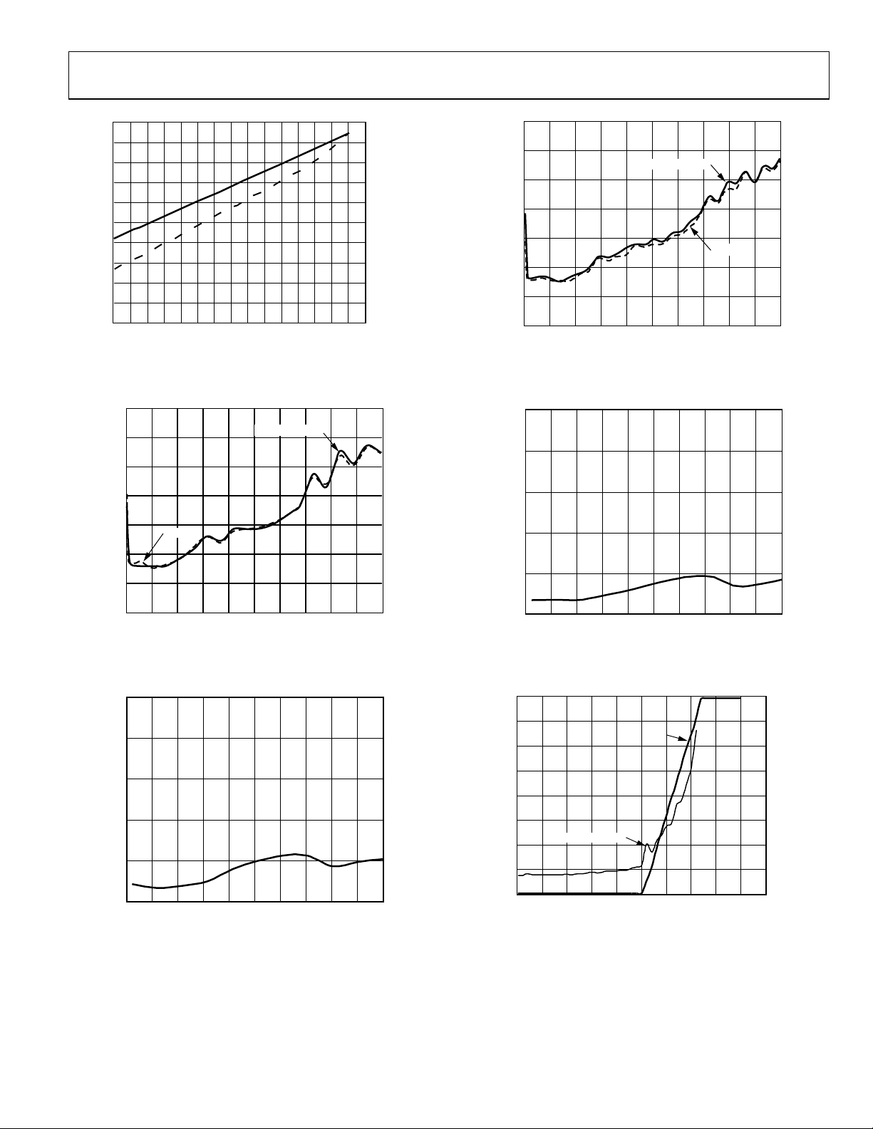
Figure 21. IMD vs. IFIN (f
= 26 MSPS)
CLK
–5
–10
–15
–20
–25
–30
–35
–40
–45
PIN (dBFS)
04319-0-021
13
12
11
10
9
NOISE FIGURE (dB)
8
7
6
50 500100 150 200 250 300 350 400 450
0
Figure 24. Noise Figure vs. Frequ ency
(Minimum Attenuation, f
16-BIT WITH DVGA
FREQUENCY (MHz)
= 18 MSPS, BW = 10 kHz)
CLK
24-BIT
04319-0-022
13
12
11
10
NOISE FIGURE (dB)
9
8
7
6
24-BIT
50 500100 150 200 250 300 350 400 450
0
Figure 22. Noise Figure vs. Frequency
(Minimum Attenuation, f
0
–2
–4
IIP3 (dBm)
–6
–8
16-BIT WITH DVGA
FREQUENCY (MHz)
= 26 MSPS, BW = 10 kHz)
CLK
04319-0-023
0
–2
–4
IIP3 (dBm)
–6
–8
–10
50 500100 150 200 250 300 350 400 450
0
Figure 25. Input IIP3 vs. Frequency (f
20.0
18.5
17.0
15.5
14.0
12.5
NOISE FIGURE (dBc)
11.0
9.5
NOISE FIGURE
FREQUENCY (MHz)
AGC
= 18 MSPS)
CLK
04319-0-025
128
112
96
80
64
48
MEAN AGC ATTN VALUE
32
16
–10
50 500100 150 200 250 300 350 400 450
0
FREQUENCY (MHz)
Figure 23. Input IIP3 vs. Frequency (f
= 26 MSPS)
CLK
04319-0-023
Rev. 0 | Page 13 of 44
8.0
–55
INTERFERER LEVEL (dBm)
–15–20–25–30–35–40–45–50
Figure 26. Noise Figure vs. Interferer Level (16-Bit Data,
BW = 12.5 kHz, AGCR = 1, f
INTERFERER
= fIF + 110 kHz)
0
–5–10
04319-0-026
AD9864
16
256
16
128
15
14
13
12
11
NOISE FIGURE (dBc)
10
9
8
–50
AGC ATTN
NOISE FIGURE
–20–25–30–35–40–45
INTERFERER LEVEL (dBm)
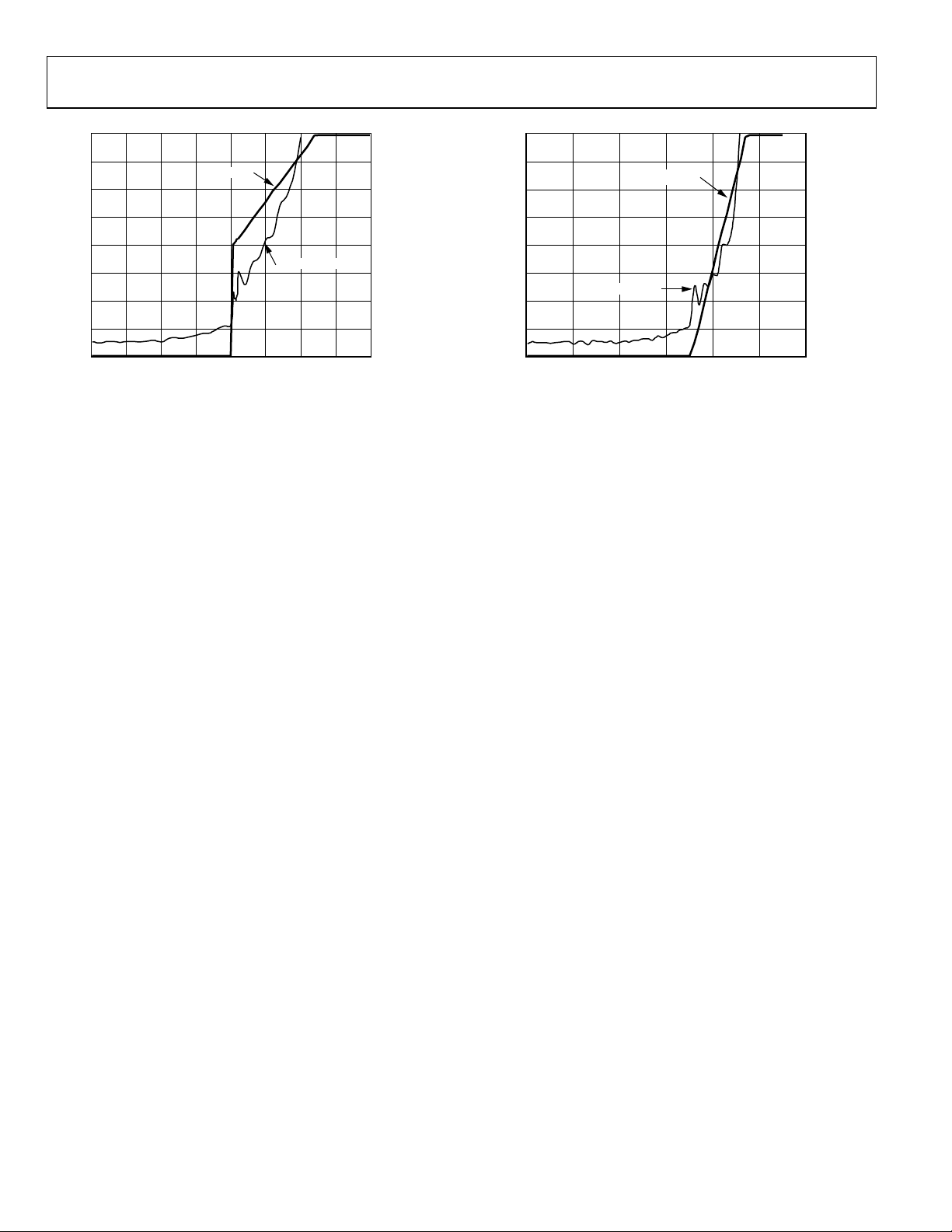
Figure 27. Noise Figure vs. Interferer Level (16-Bit Data with DVGA,
BW = 12.5 kHz, AGCR = 1, f
INTERFERER
= fIF + 110 kHz)
224
192
160
128
96
MEAN AGC ATTN VALUE
64
32
0
–10–15
04319-0-027
15
14
13
12
11
NOISE FIGURE (dBc)
10
9
8
–65
NOISE FIGURE
AGC ATTN
–25–35–45–55
INTERFERER LEVEL (dBm)
96
64
MEAN AGC ATTN VALUE
32
0
–5–15
04319-0-028
Figure 28. Noise Figure vs. Interferer Level (24-Bit Data,
BW = 12.5 kHz, AGCR = 1, f
INTERFERER
= fIF + 110 kHz)
Rev. 0 | Page 14 of 44
 Loading...