A
Mixed-Signal Front-End (MxFE™) Baseband
Transceiver for Broadband Applications
FEATURES
Receive path includes dual 12-bit, 50 MSPS analog-to-digital
converters with internal or external reference
Transmit path includes dual 12-bit, 200 MSPS digital-to-
analog converters with 1×, 2×, or 4× interpolation and
programmable gain control
Internal clock distribution block includes a programmable
phase-locked loop and timing generation circuitry,
allowing single-reference clock operation
24-pin flexible I/O data interface allows various interleaved
or noninterleaved data transfers in half-duplex mode and
interleaved data transfers in full-duplex mode
Configurable through register programmability or
optionally limited programmability through mode pins
Independent Rx and Tx power-down control pins
64-lead LFCSP package (9 mm × 9 mm footprint)
APPLICATIONS
Broadband access
Broadband LAN
Communications (modems)
GENERAL DESCRIPTION
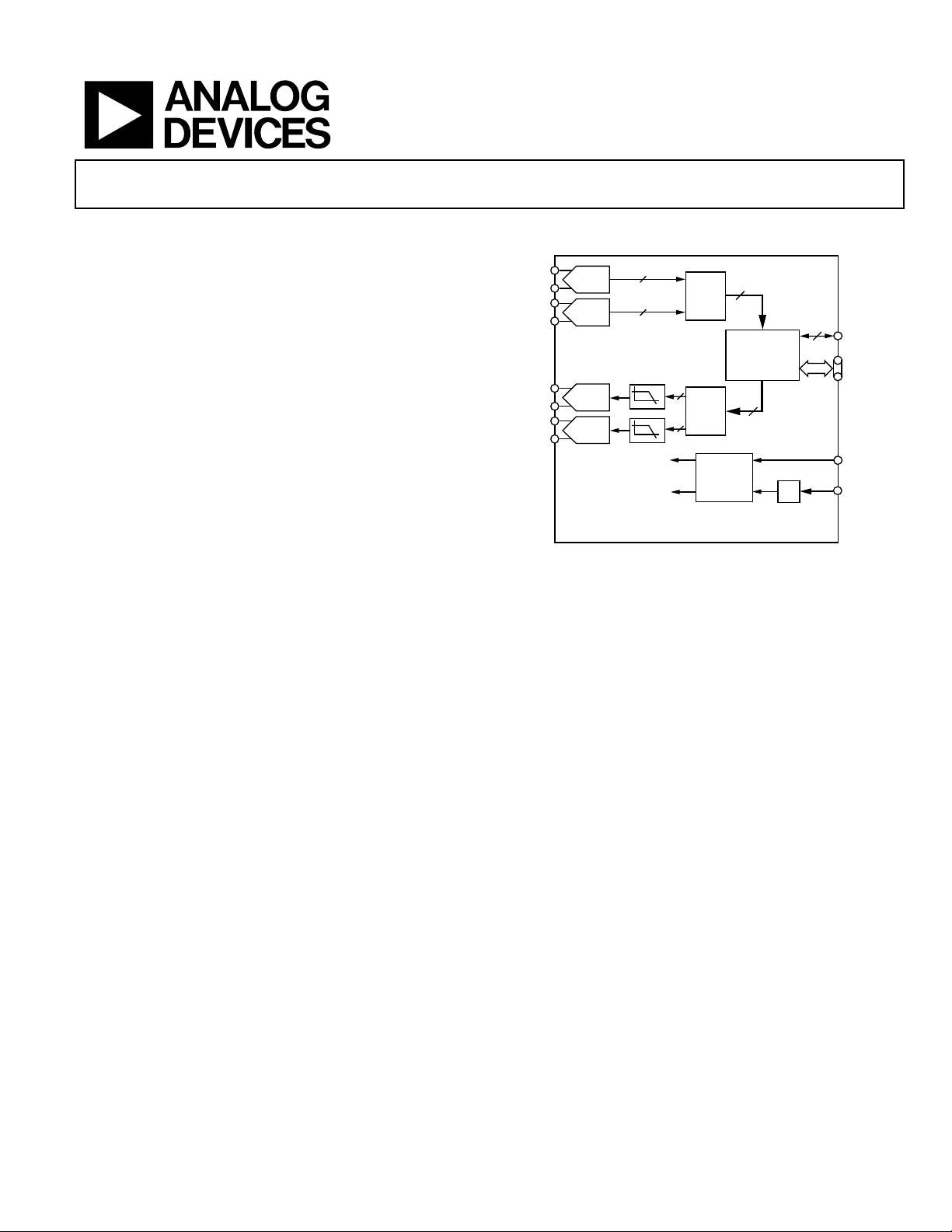
The AD9863 is a member of the MxFE family—a group of
integrated converters for the communications market. The
AD9863 integrates dual 12-bit analog-to-digital converters
(ADC) and dual 12-bit digital-to-analog converters (TxDAC®).
The AD9863 ADCs are optimized for ADC sampling of 50 MSPS
and less. The dual TxDACs operate at speeds up to 200 MHz
and include a bypassable 2× or 4× interpolation filter. The
AD9863 is optimized for high performance, low power, small
form factor, and to provide a cost-effective solution for the
broadband communication market.
The AD9863 uses a single input clock pin (CLKIN) or two
independent clocks for the Tx path and the Rx path. The ADC
and TxDAC clocks are generated within a timing generation
block that provides user programmable options such as divide
circuits, PLL multipliers, and switches.
A flexible, bidirectional 24-bit I/O bus accommodates a variety
of custom digital back ends or open market DSPs.
AD9863
FUNCTIONAL BLOCK DIAGRAM
VIN+A
VIN–A
VIN+B
VIN–B
IOUT+
IOUT–A
IOUT+B
IOUT–B
In half-duplex systems, the interface supports 24-bit parallel
transfers or 12-bit interleaved transfers. In full-duplex systems,
the interface supports an 12-bit interleaved ADC bus and an
12-bit interleaved TxDAC bus. The flexible I/O bus reduces pin
count and, therefore, reduces the required package size on the
AD9863 and the device to which it connects.
The AD9863 can use either mode pins or a serial programmable interface (SPI) to configure the interface bus, operate the
ADC in a low power mode, configure the TxDAC interpolation
rate, and control ADC and TxDAC power-down. The SPI
provides more programmable options for both the TxDAC path
(for example, coarse and fine gain control and offset control for
channel matching) and the ADC path (for example, the internal
duty cycle stabilizer, and twos complement data format).
The AD9863 is packaged in a 64-lead LFCSP (low profile, fine
pitched, chip scale package). The 64-lead LFCSP footprint is
only 9 mm × 9 mm, and is less than 0.9 mm high, fitting into
tightly spaced applications such as PCMCIA cards.
ADC
ADC
DAC
DAC
LOW-PASS
INTERPOLATION
FILTER
DAC CLOCK
AD9863
DATA
MUX
AND
LATCH
DATA
LATCH
AND
DEMUX
CLOCK
GENERATION
BLOCK
Figure 1.
Rx DATA
I/O
INTERFACE
CONFIGURATION
BLOCK
Tx DATA
PLL
I/O
INTERFACE
CONTROL
FLEXIBLE
I/O BUS
[0:23]
CLKIN1ADC CLOCK
CLKIN2
03604-0-070
Rev. 0
Information furnished by Analog Devices is believed to be accurate and reliable.
However, no responsibility is assumed by Analog Devices for its use, nor for any
infringements of patents or other rights of third parties that may result from its use.
Specifications subject to change without notice. No license is granted by implication
or otherwise under any patent or patent rights of Analog Devices. Trademarks and
registered trademarks are the property of their respective owners.
One Technology Way, P.O. Box 9106, Norwood, MA 02062-9106, U.S.A.
Tel: 781.329.4700
Fax: 781.326.8703 © 2003 Analog Devices, Inc. All rights reserved.
www.analog.com

AD9863
TABLE OF CONTENTS
Tx Path Specifications...................................................................... 3
Theory of Operation...................................................................... 18
Rx Path Specifications...................................................................... 4
Power Specifications......................................................................... 5
Digital Specifications........................................................................ 5
Timing Specifications....................................................................... 6
Absolute Maximum Ratings............................................................ 7
ESD Caution.................................................................................. 7
Pin Configuration and Pin Function Descriptions...................... 8
Typical Performance Characteristics ........................................... 10
Te r m in o l o g y .................................................................................... 17
REVISION HISTORY
Revision 0: Initial Version
System Block ............................................................................... 18
Rx Path Block.............................................................................. 18
Tx Path Block.............................................................................. 20
Digital Block................................................................................ 23
Programmable Registers............................................................ 33
Clock Distribution Block .......................................................... 36
Outline Dimensions....................................................................... 40
Ordering Guide .......................................................................... 40
Rev. 0 | Page 2 of 40
AD9863
Tx PATH SPECIFICATIONS
Table 1. F
AVDD = DVDD = 3.3 V, unless otherwise noted
Parameter Temp Test Level Min Typ Max Unit
Tx PATH GENERAL
Resolution Full IV 12 Bits
Maximum DAC Update Rate Full IV 200 MHz
Maximum Full-Scale Output Current Full IV 20 mA
Full-Scale Error Full V 1%
Gain Mismatch Error 25°C IV –3.5 +3.5 % FS
Offset Mismatch Error Full IV –0.1 +0.1 % FS
Reference Voltage Full V 1.23 V
Output Capacitance Full V 5 pF
Phase Noise (1 kHz Offset, 6 MHz Tone) 25°C V –115 dBc/Hz
Output Voltage Compliance Range Full IV –1.0 +1.0 V
TxPGA Gain Range Full V 20 dB
TxPGA Step Size Full V 0.10 dB
Tx PATH DYNAMIC PERFORMANCE
= 20 mA; F
(I
OUTFS
SNR Full IV 70.8 71.6 dB
SINAD Full IV 64.3 71 dB
THD Full IV −79 −66.3 dBc
SFDR, Wideband (DC to Nyquist) Full IV 68.5 77 dBc
SFDR, Narrowband (1 MHz Window) Full IV 72.8 81 dBc
1
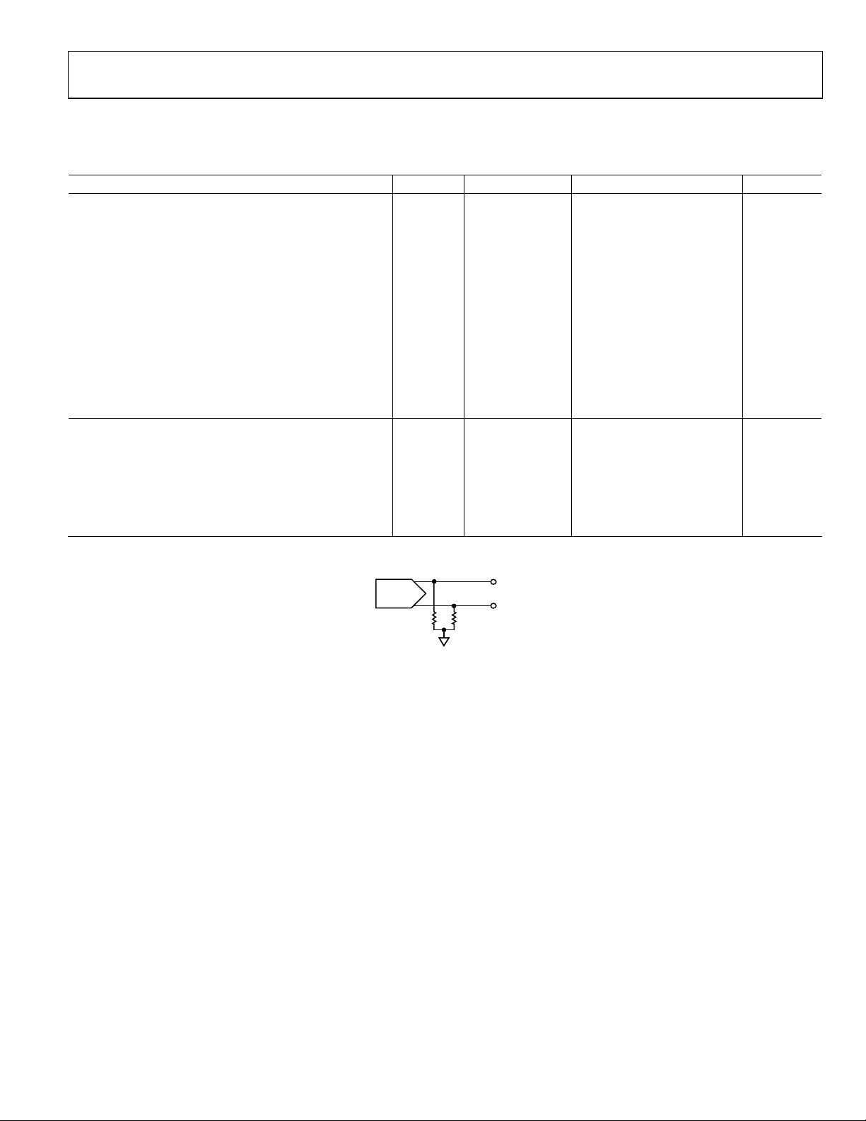
See Figure 2 for description of the TxDAC termination scheme.
= 200 MSPS; 4× interpolation; R
DAC
= 1 MHz)
OUT
= 4.02 kΩ; differential load resistance of 100 Ω1; TxPGA = 20 dB,
SET
TxDAC
50Ω 50Ω
03604-0-071
Figure 2. Diagram showing Termination of100 Ω Differential
Load for Some TxDAC Measurements
Rev. 0 | Page 3 of 40

AD9863
Rx PATH SPECIFICATIONS
Table 2. F
Parameter Temp Test Level Min Typ Max Unit
Rx PATH GENERAL
Resolution Full V 12 Bits
Maximum ADC Sample Rate Full IV 50 MSPS
Gain Mismatch Error Full V
Offset Mismatch Error Full V
Reference Voltage Full V 1.0 V
Reference Voltage (REFT–REFB) Error Full IV –30
Input Resistance (Differential) Full V 2 kΩ
Input Capacitance Full V 5 pF
Input Bandwidth Full V 30 MHz
Differential Analog Input Voltage Range Full V 2 V p-p differential
Rx PATH DC ACCURACY
Integral Nonlinearity (INL) 25°C V
Differential Nonlinearity (DNL) 25°C V
Aperature Delay 25°C V 2.0 ns
Aperature Uncertainty (Jitter) 25°C V 1.2 ps rms
Input Refered Noise 25°C V 250 uV
AD9863 Rx PATH DYNAMIC PERFORMANCE
(V
= –0.5 dBFS; FIN = 10 MHz)
IN
SNR Full V 67 dBc
SINAD Full V 65.5 dBc
THD (Second to Ninth Harmonics) Full IV −73 −66.6 dBc
SFDR, Wideband (DC to Nyquist) Full IV 68.3 74 dBc
Crosstalk between ADC Inputs Full V 80 dB
= 50 MSPS; internal reference; differential analog inputs, ADC_AVDD = DVDD = 3.3 V, unless otherwise noted
ADC
±0.2
±0.1
±6
±0.75
±0.75
% FS
% FS
+30 mV
LSB
LSB
Rev. 0 | Page 4 of 40

AD9863
POWER SPECIFICATIONS
Table 3. Analog and digital supplies = 3.3 V; F
Parameter Temp Test Level Min Typ Max Unit
POWER SUPPLY RANGE
Analog Supply Voltage (AVDD) Full IV 2.7 3.6 V
Digital Supply Voltage (DVDD) Full IV 2.7 3.6 V
Driver Supply Voltage (DRVDD)
ANALOG SUPPLY CURRENTS
TxPath (20 mA Full-Scale Outputs) Full V 70 mA
TxPath (2 mA Full-Scale Outputs) Full V 20 mA
Rx Path (50 MSPS) Full V 103 mA
RxPath (50 MSPS, Low Power Mode) Full V 69 mA
RxPath (20 MSPS, Low Power Mode) Full V 55 mA
TxPath, Power-Down Mode Full V 2 mA
RxPath, Power-Down Mode Full V 5 mA
PLL Full V 12 mA
DIGITAL SUPPLY CURRENTS
TxPath, 1× Interpolation,
50 MSPS DAC Update for Both DACs,
Half-Duplex 24 Mode
TxPath, 2× Interpolation,
100 MSPS DAC Update for Both DACs,
Half-Duplex 24 Mode
TxPath, 4× Interpolation,
200 MSPS DAC Update for Both DACs,
Half-Duplex 24 Mode
RxPath Digital, Half-Duplex 24 Mode Full V 15 mA
CLKIN1
= F
= 50 MHz; PLL 4× setting; normal timing mode
CLKIN2
Full IV 2.7 3.6 V
Full V 20 mA
Full V 50 mA
Full V 80 mA
DIGITAL SPECIFICATIONS
Table 4.
Parameter Temp Test Level Min Typ Max Unit
LOGIC LEVELS
Input Logic High Voltage, V
Input Logic Low Voltage, V
Output Logic High Voltage, VOH (1 mA Load) Full IV DRVDD – 0.6 V
Output Logic Low Voltage, VOL (1 mA Load) Full IV 0.4 V
DIGITAL PIN
Input Leakage Current Full IV 12 µA
Input Capacitance Full IV 3 pF
Minimum RESET Low Pulse Width Full IV 5 Input Clock Cycles
Digital Output Rise/Fall Time Full IV 2.8 4 ns
IH
IL
Full IV DRVDD – 0.7 V
Full IV 0.4 V
Rev. 0 | Page 5 of 40

AD9863
TIMING SPECIFICATIONS
Table 5.
Parameter Temp Test Level Min Typ Max Unit
INPUT CLOCK
CLKIN2 Clock Rate (PLL Bypassed) Full IV 1 200 MHz
PLL Input Frequency Full IV 16 200 MHz
PLL Ouput Frequency Full IV 32 350 MHz
TxPATH DATA
Setup Time
(HD24 Mode, Time Required before Data Latching Edge)
Hold Time
(HD24 Mode, Time Required after Data Latching Edge)
Latency 1× Interpolation (Data In until Peak Output Response) Full V 7 DAC Clock Cycles
Latency 2× Interpolation (Data In until Peak Output Response) Full V 35 DAC Clock Cycles
Latency 4× Interpolation (Data In until Peak Output Response) Full V 83 DAC Clock Cycles
RxPATH DATA
Output Delay (HD24 Mode, tOD) Full V –1.5
Latency Full V 5 ADC Clock Cycles
Full V 5
Full V –1.5
ns (see Clock
Distribution Block
section)
ns (see Clock
Distribution Block
section)
ns ( see Clock
Distribution Block
section)
Table 6. Explanation of Test Levels
Level Description
I 100% production tested.
II
III Sample tested only.
IV Parameter is guaranteed by design and characterization testing.
V Parameter is a typical value only.
VI
100% production tested at 25°C and guaranteed by design and characterization at specified temperatures.
100% production tested at 25°C and guaranteed by design and characterization for industrial temperature range.
Rev. 0 | Page 6 of 40
AD9863
ABSOLUTE MAXIMUM RATINGS
Table 7.
Parameter Rating
Electrical
AVDD Voltage 3.9 V max
DRVDD Voltage 3.9 V max
Analog Input Voltage –0.3 V to AVDD + 0.3 V
Digital Input Voltage –0.3 V to DVDD – 0.3 V
Digital Output Current 5 mA max
Environmental
Operating Temperature Range
(Ambient)
Maximum Junction Temperature
Lead Temperature
(Soldering, 10 sec)
Storage Temperature Range
(Ambient)
–40°C to +85°C
150°C
300°C
–65°C to +150°C
Thermal Resistance
64-lead LFCSP (4-layer board):
θ
= 24.2 (paddle soldered to ground plan, 0 LPM air)
JA
= 30.8 (paddle not soldered to ground plan, 0 LPM air)
θ
JA
Stresses above those listed under the Absolute Maximum
Ratings may cause permanent damage to the device. This is a
stress rating only; functional operation of the device at these or
any other conditions above those indicated in the operational
section of this specification is not implied. Exposure to absolute
maximum rating conditions for extended periods may affect
device reliability.
ESD CAUTION
ESD (electrostatic discharge) sensitive device. Electrostatic charges as high as 4000 V readily accumulate on the
human body and test equipment and can discharge without detection. Although this product features
proprietary ESD protection circuitry, permanent damage may occur on devices subjected to high energy
electrostatic discharges. Therefore, proper ESD precautions are recommended to avoid performance
degradation or loss of functionality.
Rev. 0 | Page 7 of 40
AD9863
A
R
PIN CONFIGURATION AND PIN FUNCTION DESCRIPTIONS
SPI_DIO
SPI_CLK
SPI_SDO
DC_LO_PW
DVDD
DVSS
AVDD
IOUT–A
IOUT+A
AGND
REFIO
FSADJ
AGND
IOUT+B
IOUT–B
AVDD
SPI_CS64TxPWRDWN63RxPWRDWN62ADC_AVDD61REFT60ADC_AVSS59VIN+A58VIN–A57VREF56VIN–B55VIN+B54ADC_AVSS53REFB52ADC_AVDD51PLL_AVDD50PLL_AVSS
1
2
3
4
5
6
7
8
9
10
11
12
13
14
15
16
18
19
U11
IFACE217IFACE3
AD9863
TOP VIEW
(Not to Scale)
20U921U822U723U624U525U426U327U228U129U030
U10
49
48
CLKIN1
CLKIN2
47
46
RESET
L0
45
L1
44
43
L2
L3
42
L4
41
40
L5
L6
39
38
L7
L8
37
L9
36
35
L10
L11
34
IFACE1
33
31
32
DRVDD
DRVSS
03604-0-072
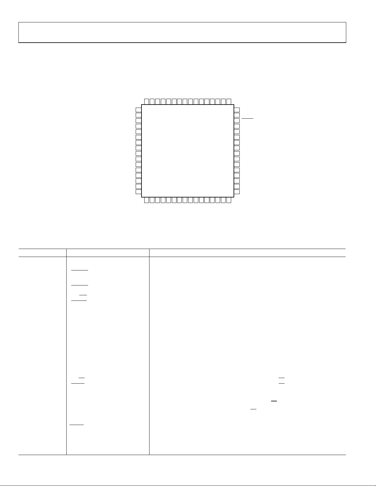
Figure 3. Pin Configuration
Table 8. Pin Function Descriptions
Pin No. Name
1
1 SPI_DIO
(
Interp1)
2 SPI_CLK
(
Interp0)
3 SPI_SDO
FD/HD)
(
Description
SPI: Serial Port Data Input.
No SPI: Tx Interpolation Pin, MSB.
SPI: Serial Port Shift Clock.
No SPI: Tx Interpolation Pin, LSB.
SPI: 4-Wire Serial Port Data Output
No SPI: Configures Full-Duplex or Half-Duplex Mode.
2, 3
4 ADC_LO_PWR ADC Low Power Mode Enable. Defined at power-up.
5, 31 DVDD, DRVDD Digital Supply.
6, 32 DVSS, DRVDD Digital Ground.
7, 16, 50, 51, 61 AVDD Analog Supply.
8, 9 IOUT-A, IOUT+A DAC A Differential Output.
10, 13, 49, 53, 59 AGND, AVSS Analog Ground.
11 REFIO Tx DAC Band Gap Reference Decoupling Pin.
12 FSADJ Tx DAC Full-Scale Adjust Pin.
14, 15 IOUT+B, IOUT−B DAC B Differential Output.
17 IFACE2
(12/24)
SPI: Buffered CLKIN. Can be configured as system clock output.
No SPI: For FD: Buffered CLKIN; For HD24 or HD12: 12/
18 IFACE3 Clock Output.
19–30 U11–U0 Upper Data Bit 11 to Upper Data Bit 0.
33 IFACE1
SPI: For FD: TxSYNC; For HD24, HD12, or Clone: Tx/Rx.
No SPI: FD >> TxSYNC; HD24 or HD12: Tx/Rx.
34–45 L11–L0 Lower Data Bit 11 to Lower Data Bit 0.
46
RESET
Chip Reset When Low.
47 CLKIN2 Clock Input 2.
48 CLKIN1 Clock Input 1
52 REFB ADC Bottom Reference.
Rev. 0 | Page 8 of 40
24 Configuration Pin.

AD9863
Pin No. Name
1
Description
2, 3
54, 55 VIN+B, VIN−B ADC B Differential Input.
56 VREF ADC Band Gap Reference.
57, 58 VIN−A, VIN+A ADC A Differential Input.
60 REFT ADC Top Reference.
62 RxPwrDwn Rx Analog Power-Down Control.
63 TxPwrDwn Tx Analog Power-Down Control.
64 SPI_CS
1
Underlined pin names and descriptions apply when the device is configured without a serial port interface, referred to as No SPI mode.
2
Some pin descriptions depend if a serial port is used (SPI mode) or not (No SPI mode), indicated by the labels SPI and No SPI.
3
Some pin descriptions depend on the interface configuration: full-duplex (FD), half-duplex interleaved data (HD12), half-duplex parallel data (HD24), and a half-duplex
interface similar to the AD9860 and AD9862 data interface called clone mode (Clone). Clone mode requires a serial port interface.
SPI: Serial Port Chip Select. At power-up or reset, this must be high.
No SPI: Tie low to disable SPI and use mode pins. This pin must be tied low.
Rev. 0 | Page 9 of 40
AD9863
TYPICAL PERFORMANCE CHARACTERISTICS
0
–10
–20
–30
40
–50
–60
–70
AMPLITUDE (dBFS)
–80
–90
–100
–110
0 5 10 15 20 25
FREQUENCY (MHz)
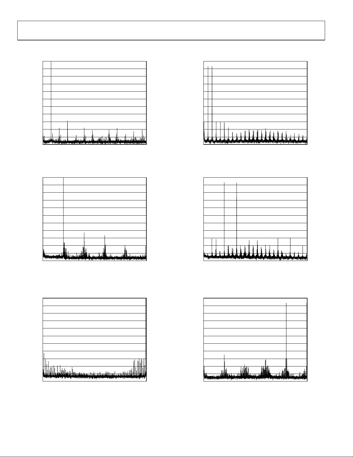
Figure 4. AD9863 Rx Path Single-Tone FFT of Rx Channel B Path
Digitizing 2 MHz Tone
03604-0-001
0
–10
–20
–30
40
–50
–60
–70
AMPLITUDE (dBFS)
–80
–90
–100
–110
0 5 10 15 20 25
FREQUENCY (MHz)
Figure 7. AD9863 Rx Path Dual-Tone FFT of Rx Channel A Path
Digitizing 1 MHz and 2 MHz Tones
03604-0-004
0
–10
–20
–30
40
–50
–60
–70
AMPLITUDE (dBFS)
–80
–90
–100
–110
0 5 10 15 20 25
FREQUENCY (MHz)
Figure 5. AD9863 Rx Path Single-Tone FFT of Rx Channel B Path
Digitizing 5 MHz Tone
0
–10
–20
–30
40
–50
–60
–70
AMPLITUDE (dBFS)
–80
–90
–100
–110
0 5 10 15 20 25
FREQUENCY (MHz)
Figure 6. AD9863 Rx Path Single-Tone FFT of Rx Channel B Path
Digitizing 24 MHz Tone
03604-0-002
03604-0-003
0
–10
–20
–30
40
–50
–60
–70
AMPLITUDE (dBFS)
–80
–90
–100
–110
0 5 10 15 20 25
FREQUENCY (MHz)
Figure 8. AD9863 Rx Path Dual-Tone FFT of Rx Channel A Path
Digitizing 5 MHz and 8 MHz Tones
0
–10
–20
–30
40
–50
–60
–70
AMPLITUDE (dBFS)
–80
–90
–100
–110
0 5 10 15 20 25
FREQUENCY (MHz)
Figure 9. AD9863 Rx Path Dual-Tone FFT of Rx Channel A Path
Digitizing 20 MHz and 25 MHz Tones
03604-0-005
03604-0-006
Rev. 0 | Page 10 of 40
AD9863
0
–10
–20
–30
40
–50
–60
–70
AMPLITUDE (dBFS)
–80
–90
–100
–110
0 5 10 15 20 25
FREQUENCY (MHz)
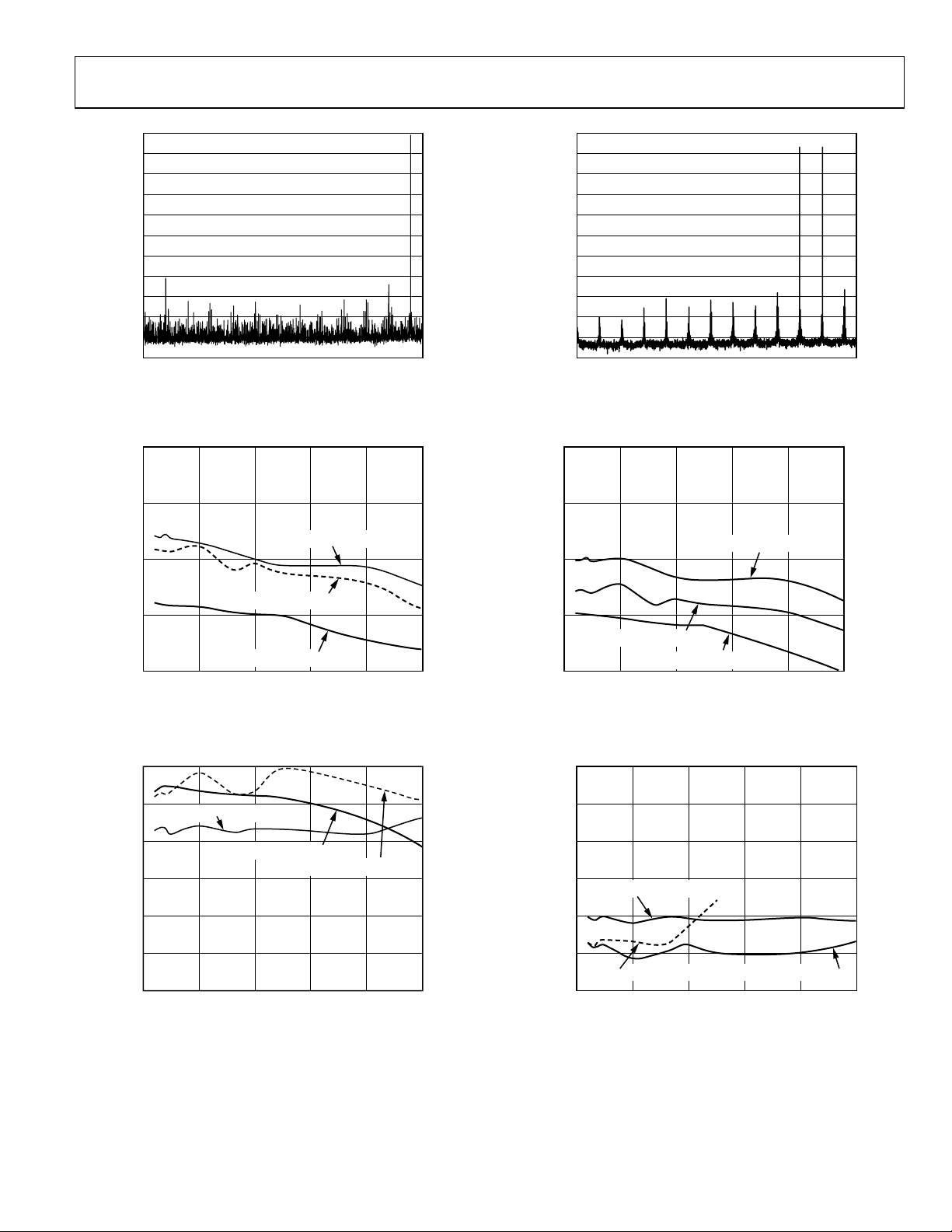
Figure 10. AD9863 Rx Path Single-Tone FFT of Rx Channel B Path
Digitizing 76 MHz Tone
03604-0-007
0
–10
–20
–30
40
–50
–60
–70
AMPLITUDE (dBFS)
–80
–90
–100
–110
0 5 10 15 20 25
FREQUENCY (MHz)
Figure 13. AD9863 Rx Path Dual-Tone FFT of Rx Channel A Path
Digitizing 70 MHz and 72 MHz Tones
03604-0-010
74
71
LOW POWER @ 25MSPS
68
SNR (dBc)
65
62
0 5 10 15 20 25
NORMAL POWER @ 50MSPS
ULTRALOW POWER @ 16MSPS
INPUT FREQUENCY (MHz)
Figure 11. AD9863 Rx Path at 50 MSPS, 10 MHz Input Tone
SNR Performance vs. Input Frequency
80
75
NORMAL POWER @ 50MSPS
70
65
SFDR (dBc)
60
ULTRALOW POWER @ 16MSPS
LOW POWER @ 25MSPS
03604-0-008
74
71
68
SINAD (dBc)
65
NORMAL POWER @ 50MSPS
62
0 5 10 15 20 25
ULTRALOW POWER @ 16MSPS
INPUT FREQUENCY (MHz)
LOW POWER @ 25MSPS
Figure 14. AD9863 Rx Path at 50 MSPS, 10 MHz Input Tone
SINAD Performance vs. Input Frequency
–50
–55
–60
–65
NORMAL POWER @ 50MSPS
THD (dBc)
–70
12.0
11.8
11.6
11.4
11.2
11.0
10.8
10.6
10.4
10.2
10.0
ENOB (Bits)
03604-0-011
55
50
0 5 10 15 20 25
INPUT FREQUENCY (MHz)
Figure 12. AD9863 Rx Path at 50 MSPS, 10 MHz Input Tone
SFDR Performance vs. Input Frequency
03604-0-009
Rev. 0 | Page 11 of 40
–75
ULTRALOW POWER @ 16MSPS
–80
0 5 10 15 20 25
INPUT FREQUENCY (MHz)
LOW POWER @ 25MSPS
Figure 15. AD9863 Rx Path at 50 MSPS, 10 MHz Input Tone
THD Performance vs. Input Frequency
03604-0-012
AD9863
80
90
–90
70
60
50
40
SNR (dBc)
30
20
10
0
0 –5 –10 –15 –20 –25 –30 –35 –40 –45 –50
INPUT AMPLITUDE (dBFS)
SNR
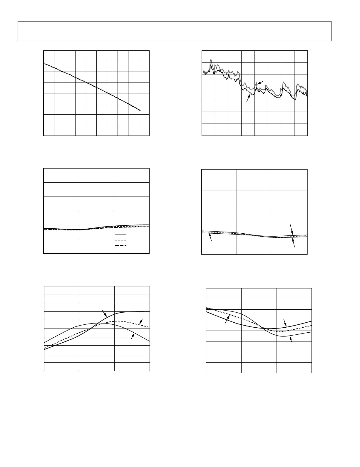
Figure 16. AD9863 Rx Path at 50 MSPS, 10 MHz Input Tone
SNR Performance vs. Input Amplitude
74
72
70
68
SNR (dBc)
66
64
62
3.6 3.3 3.0 2.7
INPUT AMPLITUDE (dBFS)
AVE –40°C
AVE +25°C
AVE +85°C
Figure 17. AD9863 Rx Path at 50 MSPS, 10 MHz Input Tone
SNR Performance vs. ADC_AVDD and Temperature
–70.0
–70.5
–71.0
–71.5
–72.0
–72.5
THD (dBc)
–73.0
–73.5
–74.0
–74.5
–75.0
2.7 3.0 3.3 3.6
INPUT AMPLITUDE (dBFS)
AVE –40°C
AVE +25°C
AVE +85°C
Figure 18. AD9863 Rx Path Single-Tone THD Performance vs.
ADC_AVDD and Temperature
03604-0-013
03604-0-014
03604-0-015
80
70
60
50
SFDR (dBFS)
40
30
20
0 –5 –10 –15 –20 –25 –30 –35 –40
THD
INPUT AMPLITUDE (dBFS)
SFDR
Figure 19. AD9863 Rx Path at 50 MSPS, 10 MHz Input Tone
THD and SFDR Performance vs. Input Amplitude
74
71
68
SINAD (dBc)
65
AVE +25°C
62
2.7 3.0 3.3 3.6
INPUT FREQUENCY (MHz)
AVE +85°C
AVE –40°C
Figure 20. AD9863 Rx Path at 50 MSPS, 10 MHz Input Tone
SINAD Performance vs. ADC_AVDD and Temperature
78
77
76
75
AVE +25°C
74
SFDR (dBc)
73
72
71
70
2.7 3.0 3.3 3.6
INPUT AMPLITUDE (dBFS)
AVE +85°C
AVE –40°C
Figure 21. AD9863 Rx Path Single-Tone SFDR Performance vs.
ADC_AVDD and Temperature
–80
–70
–60
–50
–40
–30
–20
12.0
11.8
11.6
11.4
11.2
11.0
10.8
10.6
10.4
10.2
10.0
THD (dBFS)
03604-0-016
ENOB (Bits)
03604-0-017
03604-0-018
Rev. 0 | Page 12 of 40
 Loading...