ANALOG DEVICES AD9862 Service Manual
Mixed-Signal Front-End (MxFE™) Processor
www.BDTIC.com/ADI
a
FEATURES
Mixed-Signal Front-End Processor with Dual Converter
Receive and Dual Converter Transmit Signal Paths
Receive Signal Path Includes:
Two 10-/12-Bit, 64 MSPS Sampling A/D Converters
with Internal or External Independent References,
Input Buffers, Programmable Gain Amplifiers,
Low-Pass Decimation Filters, and a Digital Hilbert Filter
Transmit Signal Path Includes:
Two 12-/14-Bit, 128 MSPS D/A Converters with
Programmable Full-Scale Output Current, Channel
Independent Fine Gain and Offset Control, Digital
Hilbert and Interpolation Filters, and Digitally Tunable
Real or Complex Up-Converters
Delay-Locked Loop Clock Multiplier and Integrated
Timing Generation Circuitry Allow for Single Crystal
or Clock Operation
Programmable Output Clocks, Serial Programmable
Interface, Programmable Sigma-Delta, Three Auxiliary
DAC Outputs and Two Auxiliary ADCs with Dual
Multiplexed Inputs
APPLICATIONS
Broadband Wireless Systems
Fixed Wireless, WLAN, MMDS, LMDS
Broadband Wireline Systems
Cable Modems, VDSL, PowerPlug
Digital Communications
Set-Top Boxes, Data Modems
GENERAL DESCRIPTION
The AD9860 and AD9862 (AD9860/AD9862) are versatile
integrated mixed-signal front-ends (MxFE) that are optimized
for broadband communication markets. The AD9860/AD9862
are cost effective, mixed signal solutions for wireless or wireline
standards based or proprietary broadband modem systems where
dynamic performance, power dissipation, cost, and size are all
critical attributes. The AD9860 has 10-bit ADCs and 12-bit DACs;
the AD9862 has 12-bit ADCs and 14-bit DACs.
The AD9860/AD9862 receive path (Rx) consists of two channels
that each include a high performance, 10-/12-bit, 64 MSPS analogto-digital converter (ADC), input buffer, Programmable Gain
Amplifier (RxPGA), digital Hilbert filter, and decimation filter. The
Rx can be used to receive real, diversity, or I/Q data at baseband or
low IF. The input buffers provide a constant input impedance for
both channels to ease impedance matching with external components (e.g., SAW filter). The RxPGA provides a 20 dB gain
*Protected by U.S.Patent No. 5,969,657; other patents pending.
MxFE is a trademark of Analog Devices, Inc.
REV. 0
Information furnished by Analog Devices is believed to be accurate and
reliable. However, no responsibility is assumed by Analog Devices for its
use, nor for any infringements of patents or other rights of third parties that
may result from its use. No license is granted by implication or otherwise
under any patent or patent rights of Analog Devices.
for Broadband Communications
AD9860/AD9862
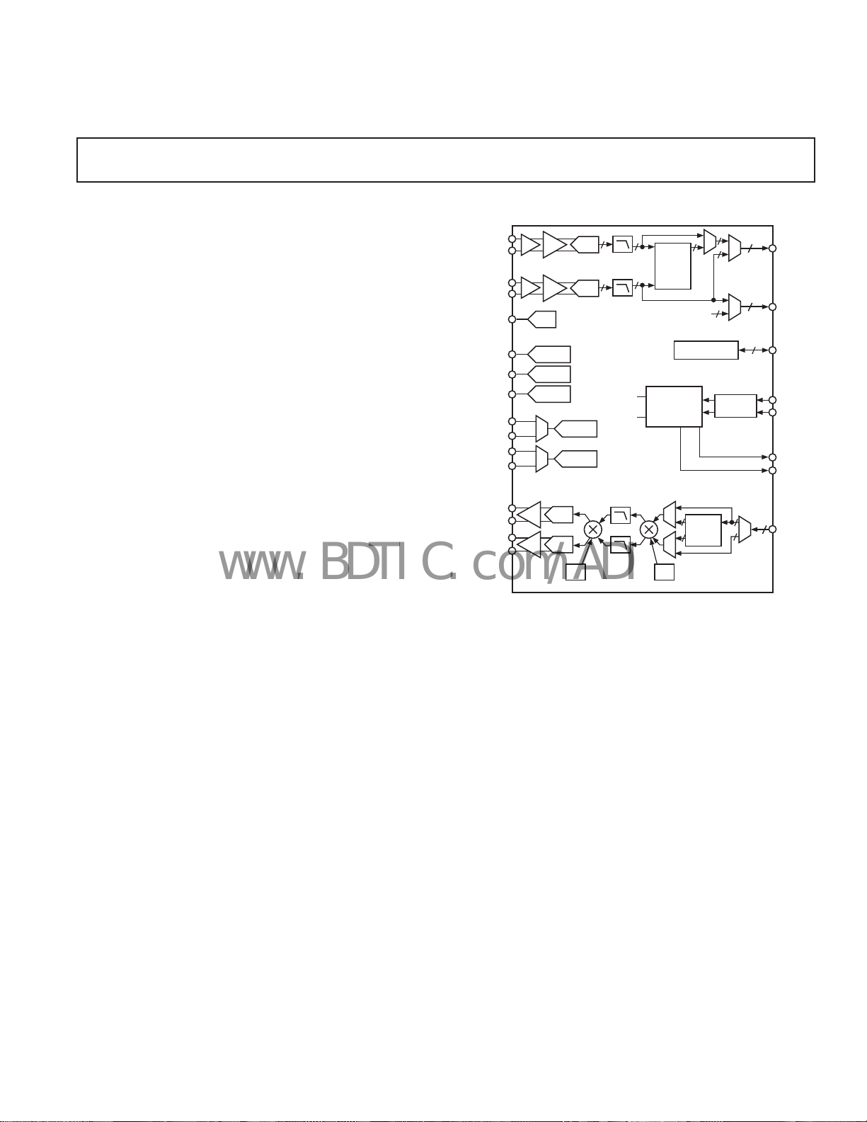
FUNCTIONAL BLOCK DIAGRAM
VIN+A
VIN–A
VIN+B
VIN–B
SIGDELT
AUX _DAC_ A
AUX _DAC_ B
AUX _DAC_ C
AUX_ADC_A1
AUX_ADC_A2
AUX_ADC_B1
AUX_ADC_B2
IOUT+A
IOUT–A
IOUT+B
IOUT–B
range for both channels. The output data bus can be multiplexed to accommodate a variety of interface types.
The AD9860/AD9862 transmit path (Tx) consists of two channels that contain high performance, 12-/14-bit, 128 MSPS
digital-to-analog converters (DAC), programmable gain amplifiers
(TxPGA), interpolation filters, a Hilbert filter, and digital mixers
for complex or real signal frequency modulation. The Tx latch
and demultiplexer circuitry can process real or I/Q data. Interpolation rates of 2 and 4 are available to ease requirements on
an external reconstruction filter. For single channel systems, the
digital Hilbert filter can be used with an external quadrature
modulator to create an image rejection architecture. The two
12-/14-bit, high performance DACs produce an output signal
that can be scaled over a 20 dB range by the TxPGA.
A programmable delay-locked loop (DLL) clock multiplier and
integrated timing circuits enable the use of a single external
reference clock or an external crystal to generate clocking for all
internal blocks and also provides two external clock outputs.
Additional features include a programmable sigma-delta output,
four auxiliary ADC inputs and three auxiliary DAC outputs.
Device programmability is facilitated by a serial port interface
(SPI) combined with a register bank. The AD9860/AD9862 is
available in a space saving 128-lead LQFP.
One Technology Way, P.O. Box 9106, Norwood, MA 02062-9106, U.S.A.
Tel: 781/329-4700www.analog.com
Fax: 781/326-8703 © Analog Devices, Inc., 2002
1x
1x
PGA
PGA
PGA
PGA
-
AUX DAC
AUX DAC
AUX DAC
DAC
DAC
ADC
BYPASSABLE LOW-PASS
DECIMATION FILTER
ADC
AD9860/AD9862
Rx PATH
TIMING
Tx PATH
BYPASSABLE
DIGITAL
QUADRATURE
MIXER
BYPASSABLE
FS/4
LOW-PASS
FS/8
INTERPOLATION
TIMING
BYPASSABLE
QUADRATURE
FILTER
AUX ADC
AUX ADC
HILBERT
FILTER
CLOCK
DISTRIBUTION
BLOCK
DIGITAL
MIXER
NCO
LOGIC LOW
SPI REGISTERS
HILBERT
FILTER
DLL
1, 2, 4
*
RxA DATA
[0:11]
RxB DATA
[0:11]
SPI
INTERFACE
OSC1
OSC2
CLKOUT1
CLKOUT2
Tx DATA
[0:13]
AD9860/AD9862–SPECIFICATIONS
www.BDTIC.com/ADI
(VA = 3.3 V 5%, VD = 3.3 V 10%, f
Normal Timing Mode, 2 DLL Setting, R
= 128 MHz, f
DAC
= 4 k, 50 DAC Load,
SET
= 64 MHz
ADC
RxPGA = +6 dB Gain, TxPGA = +20 dB Gain.)
Tx PARAMETERS Temp Level Min Typ Max Unit
12-/14-BIT DAC CHARACTERISTICS
Resolution NA NA 12/14 Bits
Maximum Update Rate 128 MSPS
Full-Scale Output Current Full I 2 20 mA
Gain Error (Using Internal Reference) 25ºCI –5.5 +0.5 +5.5 %FS
Offset Error 25ºCI –1 0.0 +1 %FS
Reference Voltage (REFIO Level) 25ºCI 1.15 1.22 1.28 V
Negative Differential Nonlinearity (–DNL) 25ºC III –0.5/–0.5 LSB
Positive Differential Nonlinearity (+DNL) 25ºC III 1/2 LSB
Integral Nonlinearity (INL) 25ºC III ±1/±3 LSB
Output Capacitance 25ºC III 5 pF
Phase Noise @ 1 kHz Offset, 6 MHz Tone
Crystal and OSC IN Multiplier Enabled at 4 25ºC III –115 dBc/Hz
Output Voltage Compliance Range Full II –0.5 +1.5 V
TRANSMIT TxPGA CHARACTERISTICS
Gain Range 25ºC III 20 dB
Step Size Accuracy 25ºC III ±0.1 dB
Step Size 25ºC III 0.08 dB
Tx DIGITAL FILTER CHARACTERISTICS
Hilbert Filter Pass Band (<0.1 dB Ripple) Full II 12.5 38 % f
2/4 Interpolator Stop Band
DYNAMIC PERFORMANCE (A
Differential Phase 25ºC III <0.1 Degree
Differential Gain 25ºC III <1 LSB
AD9860 Signal-to-Noise Ratio (SNR) Full I 68.2 70.7 dB
AD9860 Signal-to-Noise and Distortion Ratio Full I 62.5 66.1 dB
AD9860 Total Harmonic Distortion (THD) Full I –74.5 –64.0 dB
AD9860 Wideband SFDR (to Nyquist)
1 MHz Analog Out, I
1 MHz Analog Out, I
6 MHz Analog Out, I
AD9860 Narrowband SFDR (1 MHz Window)
1 MHz Analog Out, I
1 MHz Analog Out, I
AD9862 Signal-to-Noise Ratio (SNR) Full I 68.9 72.0 dB
AD9862 Signal-to-Noise and Distortion Ratio Full I 64.75 69.8 dB
AD9862 Total Harmonic Distortion (THD) Full I –75.5 –65.0 dB
AD9862 Wideband SFDR (to Nyquist)
1 MHz Analog Out, I
1 MHz Analog Out, I
6 MHz Analog Out, I
AD9862 Narrowband SFDR (1 MHz Window)
1 MHz Analog Out, I
1 MHz Analog Out, I
Rx PARAMETERS
RECEIVE BUFFER
Input Resistance (Differential) Full III 200 W
Input Capacitance (Each Input) Full III 5 pF
Maximum Input Bandwidth (–3 dB) Full III 140 MHz
Analog Input Range (Best Noise Performance) Full II 2 V p-p Diff
Analog Input Range (Best THD Performance) Full II 1 V p-p Diff
RECEIVE PGA CHARACTERISTICS
Gain Error 25ºCI ± 0.3 dB
Gain Range 25ºCI 19 20 21 dB
Step Size Accuracy 25ºCI ± 0.2 dB
Step Size 25ºCI 1 dB
Input Bandwidth (–3 dB, Rx Buffer Bypassed) 25ºC III 250 MHz
10-/12-BIT ADC CHARACTERISTICS
Resolution NA NA 10/12 Bits
Maximum Conversion Rate Full I 64
2
= 20 mA FS, f = 1 MHz)
OUT
= 2 mA 25ºC III 70.6 dBc
OUT
= 20 mA 25ºCI 64.4 75 dBc
OUT
= 20 mA 25ºC III 75 dBc
OUT
= 2 mA 25ºC III 70.2 dBc
OUT
= 20 mA 25ºCI 83 90 dBc
OUT
= 2 mA 25ºC III 70.6 dBc
OUT
= 20 mA 25ºCI 64.9 76.0 dBc
OUT
= 20 mA 25ºC III 76.0 dBc
OUT
= 2 mA 25ºC III 70.2 dBc
OUT
= 20 mA 25ºCI 83 90 dBc
OUT
Full II ±38 % f
Test AD9860/AD9862
DATA
DATA
MHz
1
REV. 0–2–
AD9860/AD9862
www.BDTIC.com/ADI
Test AD9860/AD9862
Rx PARAMETERS (continued) Temp Level Min Typ Max Unit
DC ACCURACY
Differential Nonlinearity 25ºC III ±0.3/±0.4 LSB
Integral Nonlinearity 25ºC III ±1.2/±5 LSB
Offset Error 25ºC III ±0.1 %FSR
Gain Error 25ºC III ±0.2 %FSR
Aperture Delay 25ºC III 2.0 ns
Aperture Uncertainty (Jitter) 25ºC III 1.2 ps rms
Input Referred Noise 25ºC III 250 µV
Reference Voltage Error
REFT-REFB Error (1 V) 25ºCI ±1 ± 4mV
AD9860 DYNAMIC PERFORMANCE (A
Signal-to-Noise Ratio 25∞CI 59.0 60.66 dBc
Signal-to-Noise and Distortion Ratio 25∞CI 56.0 58.0 dBc
Total Harmonic Distortion 25∞CI –76.5 –70.5 dBc
Spurious Free Dynamic Range 25∞CI 70.3 81.0 dBc
AD9862 DYNAMIC PERFORMANCE (A
Signal-to-Noise Ratio 25∞CI 62.6 64.2 dBc
Signal-to-Noise and Distortion Ratio 25∞CI 62.5 64.14 dBc
Total Harmonic Distortion 25∞CI –79.22 –73.2 dBc
Spurious Free Dynamic Range 25∞CI 77.09 85.13 dBc
CHANNEL-TO-CHANNEL ISOLATION
Tx-to-Rx (A
Rx Channel Crosstalk (f1 = 6 MHz, f2 = 9 MHz) 25ºC III >80 dB
PARAMETERS
CMOS LOGIC INPUTS
Logic “1” Voltage, V
Logic “0” Voltage, V
Logic “1” Current 25ºCII 12 µA
Logic “0” Current 25ºCII 12 µA
Input Capacitance 25ºC III 3 pF
CMOS LOGIC OUTPUTS (1 mA Load)
Logic “1” Voltage, V
Logic “0” Voltage, V
POWER SUPPLY
Analog Supply Currents
Tx (Both Channels, 20 mA FS Output) 25ºCI 70 76 mA
Tx Powered Down 25ºCI 2.5 5.0 mA
Rx (Both Channels, Input Buffer Enabled) 25ºCI 275 307 mA
Rx (Both Channels, Input Buffer Disabled) 25ºC III 245 mA
Rx (32 MSPS, Low Power Mode, Buffer Disabled) 25ºC III 155 mA
Rx (16 MSPS, Low Power Mode, Buffer Disabled) 25ºC III 80 mA
Rx Path Powered Down 25ºCI 5.0 6.0 mA
DLL 25ºC III 12 mA
Digital Supply Current
AD9860 Both Rx and Tx Path (All Channels Enabled)
2 Interpolation, f
AD9862 Both Rx and Tx Path (All Channels Enabled)
2 Interpolation, f
Tx Path (f
Processing Blocks Disabled 25ºC III 45 mA
4 Interpolation 25ºC III 90 mA
4 Interpolation, Coarse Modulation 25ºC III 110 mA
4 Interpolation, Fine Modulation 25ºC III 110 mA
4 Interpolation, Coarse and Fine Modulation 25ºC III 130 mA
= 0 dBFS, f
OUT
IH
IL
OH
OL
= 128 MSPS)
DAC
= 7 MHz) 25ºC III >90 dB
OUT
= f
DAC
ADC
= f
DAC
ADC
= –0.5 dBFS, f = 5 MHz)
IN
= –0.5 dBFS, f = 5 MHz)
IN
25ºCII
25ºCII 0.4 V
25ºCII
25ºCII 0.4 V
= 64 MSPS 25ºCI 92 112 mA
= 64 MSPS 25ºCI 104 124 mA
DRVDD – 0.7
DRVDD – 0.6
V
V
REV. 0
–3–

AD9860/AD9862
www.BDTIC.com/ADI
PARAMETERS (continued) Temp Level Min Typ Max Unit
Test AD9860/AD9862
POWER SUPPLY (continued)
Rx Path (f
= 64 MSPS)
ADC
Processing Blocks Disabled 25ºC III 9 mA
Decimation Filter Enabled 25ºC III 15 mA
Hilbert Filter Enabled 25ºC III 16 mA
Hilbert and Decimation Filter Enabled 25ºC III 18.5 mA
NOTES
1
% f
refers to the input data rate of the digital block.
DATA
2
Interpolation filter stop band is defined by image suppression of 50 dB or greater.
Specifications subject to change without notice.
TIMING CHARACTERISTICS
(20 pF Load) Temp Level Min Typ Max Unit
Minimum Reset Pulsewidth Low (t
)NANA5 Clock Cycles
RL
Digital Output Rise/Fall Time 25ºC III 2.8 4 ns
DLL Output Clock 25ºC III 32 128 MHz
DLL Output Duty Cycle 25ºC III 50 %
Tx–/Rx–Interface (See Figures 11 and 12)
, t
TxSYNC/TxIQ Setup Time (t
TxSYNC/TxIQ Hold Time (t
RxSYNC/RxIQ/IF to Valid Time(t
RxSYNC/RxIQ/IF Hold Time (t
)25ºC III 3 ns
Tx1
Tx3
, t
)25ºC III 3 ns
Tx2
Tx4
, t
)25ºC III 5.2 ns
Rx1
Rx3
, t
)25ºC III 0.2 ns
Rx2
Rx4
Serial Control Bus (See Figures 1 and 2)
Maximum SCLK Frequency (f
Minimum Clock Pulsewidth High (t
Minimum Clock Pulsewidth Low (t
) Full III 16 MHz
SCLK
) Full III 30 ns
HI
) Full III 30 ns
LOW
Maximum Clock Rise/Fall Time Full III 1 ms
Minimum Data/SEN Setup Time (t
Minimum SEN/Data Hold Time (t
Minimum Data/SCLK Setup Time (t
Minimum Data Hold Time (t
) Full III 25 ns
S
) Full III 0 ns
H
) Full III 25 ns
DS
) Full III 0 ns
DH
Output Data Valid/SCLK Time (tDV) Full III 30 ns
AUXILARY ADC
Conversion Rate 25ºC III 1.25 MHz
Input Range 25ºC III 3 V
Resolution 25ºC III 10 Bits
AUXILARY DAC
Settling Time 25ºC III 8 ms
Output Range 25ºC III 3 V
Resolution 25ºC III 8 Bits
ADC TIMING
Latency (All Digital Processing Blocks Disabled) 25ºC III 7 Cycles
DAC Timing
Latency (All Digital Processing Blocks Disabled) 25ºC III 3 Cycles
Latency (2 Interpolation Enabled) 25ºC III 30 Cycles
Latency (4 Interpolation Enabled) 25ºC III 72 Cycles
Additional Latency (Hilbert Filter Enabled) 25ºC III 36 Cycles
Additional Latency (Coarse Modulation Enabled) 25ºC III 5 Cycles
Additional Latency (Fine Modulation Enabled) 25ºC III 8 Cycles
Output Settling Time (TST) (to 0.1%) 25ºC III 35 ns
Specifications subject to change without notice.
Test AD9860/AD9862
REV. 0–4–

AD9860/AD9862
www.BDTIC.com/ADI
ABSOLUTE MAXIMUM RATINGS
Power Supply (VAS, VDS) . . . . . . . . . . . . . . . . . . . . . . . . . 3.9 V
Digital Output Current . . . . . . . . . . . . . . . . . . . . . . . . . . 5 mA
Digital Inputs . . . . . . . . . . . . . . . . –0.3 V to DRVDD + 0.3 V
Analog Inputs . . . . . . . . . . . . . . –0.3 V to AVDD (IQ) + 0.3 V
Operating Temperature
2
. . . . . . . . . . . . . . . . . –40C to +70C
Maximum Junction Temperature . . . . . . . . . . . . . . . . . 150C
Storage Temperature . . . . . . . . . . . . . . . . . . . –65C to +150C
Lead Temperature (Soldering 10 sec) . . . . . . . . . . . . . . 300C
NOTES
1
Absolute maximum ratings are limiting values, to be applied individually, and
beyond which the serviceability of the circuit may be impaired. Functional operability
under any of these conditions is not necessarily implied. Exposure to absolute
maximum rating conditions for extended periods of time may affect device
reliability.
2
The AD9860/AD9862 have been characterized to operate over the industrial
temperature range (–40C to +85C) when operated in Half Duplex Mode.
1
EXPLANATION OF TEST LEVELS
I. Devices are 100% production tested at 25ºC and guaranteed
by design and characterization testing for the extended
industrial temperature range (–40ºC to +70ºC).
II. Parameter is guaranteed by design and/or characterization
testing.
III. Parameter is a typical value only.
NA. Test level definition is not applicable.
THERMAL CHARACTERISTICS
Thermal Resistance
128-Lead LQFP JA = 29ºC/W
ORDERING GUIDE
Model Temperature Range Package Description Package Option
AD9860BST –40∞C to +70∞C* 128-Lead Low Profile Plastic Quad Flatpack (LQFP) ST-128B
AD9862BST –40∞C to +70∞C* 128-Lead Low Profile Plastic Quad Flatpack (LQFP) ST-128B
AD9860PCB Evaluation Board with AD9860
AD9862PCB Evaluation Board with AD9862
*The AD9860/AD9862 have been characterized to operate over the industrial temperature range (–40 C to +85C) when operated in Half Duplex Mode.
CAUTION
ESD (electrostatic discharge) sensitive device. Electrostatic charges as high as 4000 V readily
accumulate on the human body and test equipment and can discharge without detection. Although the
AD9860/AD9862 features proprietary ESD protection circuitry, permanent damage may occur on
devices subjected to high energy electrostatic discharges. Therefore, proper ESD precautions are
recommended to avoid performance degradation or loss of functionality.
REV. 0
–5–
AD9860/AD9862
www.BDTIC.com/ADI
AUX_ADC_A1
SIGDELT
AUX _DAC_A
AUX _DAC_B
AUX _DAC_C
DLL_Lock
Tx11/13 (MSB)
AGND
AV DD
AV DD
AGND
AGND
NC
AV DD
OSC1
OSC2
AGND
CLKSEL
AV DD
AGND
AV DD
REFIO
FSADJ
AV DD
AGND
IOUT–A
IOUT+A
AGND
AGND
IOUT+B
IOUT–B
AGND
AV DD
DVD D
DGND
DGND
DVD D
Tx10/12
1
2
3
4
5
6
7
8
9
10
11
12
13
14
15
16
17
18
19
20
21
22
23
24
25
26
27
28
29
30
31
32
33
34
35
36
37
38
AUX_ADC_B1
AUX_ADC_REF
AUX_ADC_A2
127
126
128
PIN 1
IDENTIFIER
39
40
414243
Tx7/9
Tx9/11
Tx8/10
AV DD
AV DD
AUX_ADC_B2
123
125
124
4445464748
Tx6/8
Tx5/7
Tx4/6
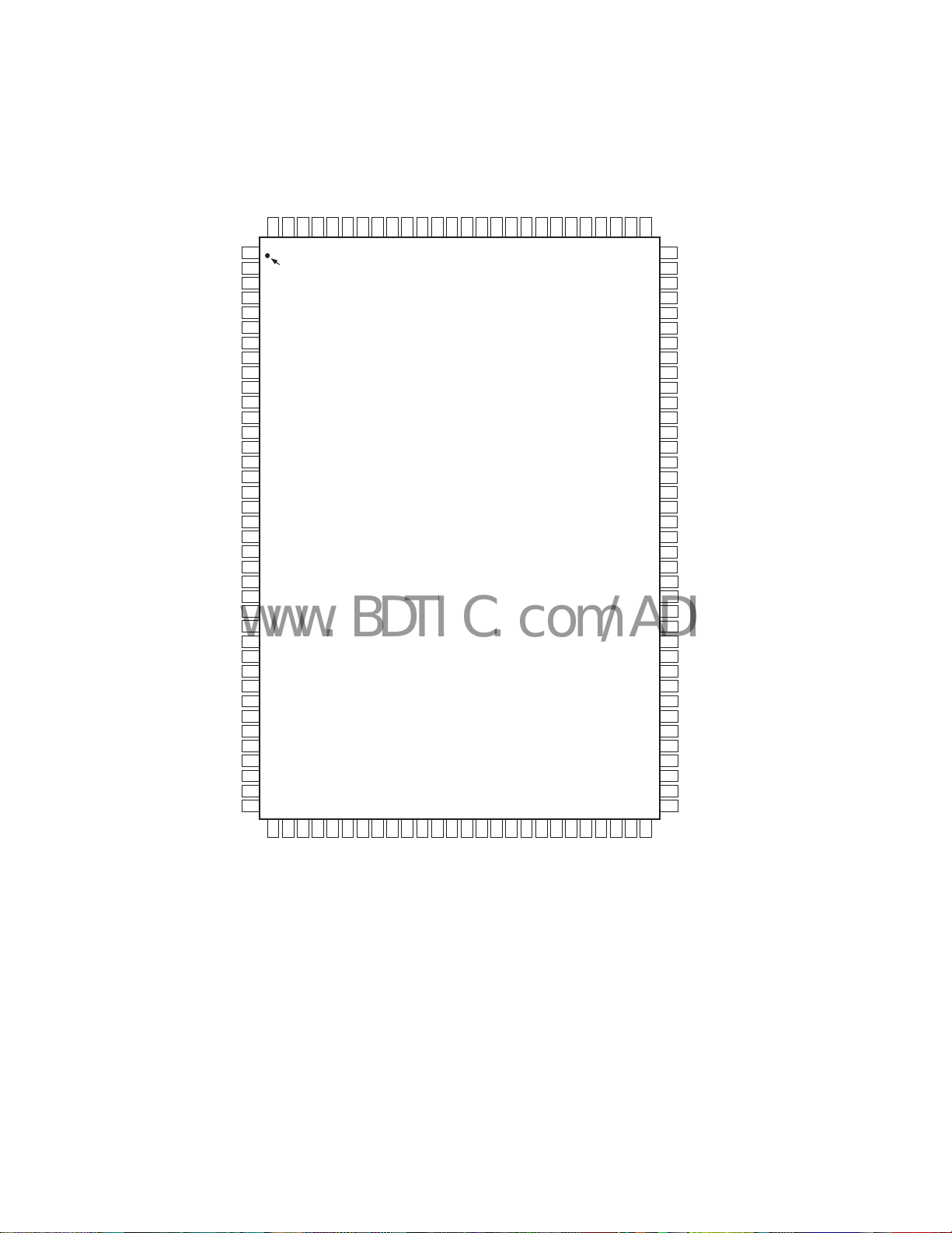
PIN CONFIGURATION
AGND
VIN–A
VIN+A
AGND
AV DD
AV DD
AGND
REFB_A
REFT_A
AGND
122
121
120
119
118
117
116
115
114
113
AD9860/AD9862
TOP VIEW
(Not to Scale)
50
53
54
51
49
52
Tx3/5
Tx2/4
Tx1/3
Tx0/2
NC/Tx1
NC/Tx0
DGND
TxSYNC
SCLK
DVD D
AGND
112
55
SDO
VREF
111
56
SDIO
AGND
110
57
SEN
AGND
109
58
DGND
VIN+B
VIN–B
108
107
59
60
DVD D
DGND
AGND
106
61
DVD D
AV DD
105
62
AGND
AV DD
104
103
64
63
RESETB
CLKOUT2
REFB_B
102
REFT_B
101
AGND
100
AV DD
99
AV DD
98
AUX_SPI_csb
97
AUX _SPI_clk
96
AUX _SPI_do
95
DGND
94
DVD D
93
RxSYNC
92
D9/D11B (MSB)
91
D8/D10B
90
D7/D9B
89
D6/D8B
88
D5/D7B
87
D4/D6B
86
D3/D5B
85
D2/D4B
84
83
D1/D3B
D0/D2B
82
NC/D1B
81
NC/D0B
80
D9/D11A (MSB)
79
D8/D10A
78
D7/D9A
77
D6/D8A
76
75
D5/D7A
74
D4/D6A
73
D3/D5A
72
D2/D4A
D1/D3A
71
70
D0/D2A
69
NC/D1A
68
NC/D0A
67
DGND
66
DVD D
65
CLKOUT1
NC = NO CONNECT
MODE/TxBLANK
REV. 0–6–
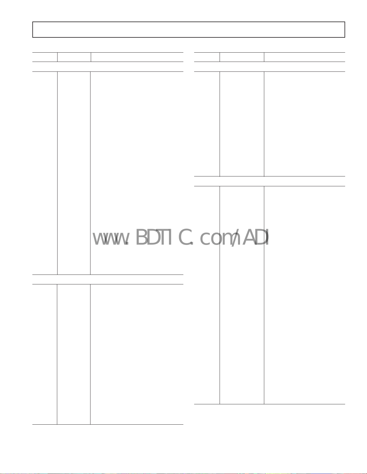
PIN FUNCTION DESCRIPTIONS
www.BDTIC.com/ADI
AD9860/AD9862
Pin No. Mnemonic Function
Receive Pins
68/70–79 D0A to 10-/12-Bit ADC Output of
D9A/D11A Receive Channel A
80/82–91 D0B to 10-/12-Bit ADC Output of
D9B/D11B Receive Channel B
92 RxSYNC Synchronization Clock for
Channel A and Channel B Rx Paths
98, 99, AVDD Analog Supply Pins
104, 105,
117, 118,
123, 124,
100, 103, AGND Analog Ground Pins
106, 109,
110, 112,
113, 116,
119, 122,
101 REFT_B Top Reference Decoupling for
Channel B ADC
102 REFB_B Bottom Reference Decoupling
for Channel B ADC
107 VIN+B Receive Channel B Differential (+) Input
108 VIN–B Receive Channel B Differential (
111 VREF Internal ADC Voltage Reference
114 VIN–A Receive Channel A Differential (
115 VIN+A Receive Channel A Differential (+) Input
120 REFB_A Bottom Reference Decoupling for
Channel A ADC
121 REFT_A Top Reference Decoupling for
Channel A ADC
Transmit Pins
18, 20 AVDD Analog Supply Pins
23, 32
19, 24, AGND Analog Ground Pins
27, 28, 31
21 REFIO Reference Output, 1.2 V Nominal
22 FSADJ Full-Scale Current Adjust
25 IOUT–ATransmit Channel A DAC
Differential (
26 IOUT+A Transmit Channel A DAC
Differential (+) Output
29 IOUT+B Transmit Channel B DAC
Differential (+) Output
30 IOUT–BTransmit Channel B DAC
Differential (
37–48/50 Tx11/Tx13 12-/14-Bit Transmit DAC Data
to Tx0 (Interleaved Data when Required)
51 TxSYNC Synchronization Input for Transmitter
62 MODE/ Configures Default Timing Mode,
TxBLANK* Controls Tx Digital Power Down
*The logic level of the Mode/TxBLANK pin at power up defines the default timing
mode; a logic low configures Normal Operation, logic high configures Alternate
Operation Mode.
) Output
) Output
) Input
) Input
Pin No. Mnemonic Function
Clock Pins
10 DLL_Lock DLL Lock Indicator Pin
11, 16 AGND DLL Analog Ground Pins
12 NC No Connect
13 AVDD DLL Analog Supply Pin
14 OSC1 Single Ended Input Clock
(or Crystal Oscillator Input)
15 OSC2 Crystal Oscillator Input
17 CLKSEL Controls CLKOUT1 Rate
64 CLKOUT2 Clock Output Generated from Input
Clock (DLL Multiplier Setting
and CLKOUT2 Divide Factor)
65 CLKOUT1 Clock Output Generated from
Input Clock (1 if CLKSEL = 1
or /2 if CLKSEL = 0)
Various Pins
1 AUX_ADC_A1 Auxiliary ADC A Input 1
3, 4, 13 AVDD Analog Power Pins
2, 9 AGND Analog Ground Pins
5 SIGDELT Digital Output from
Programmable Sigma-Delta
6 AUX_DAC_A Auxiliary DAC A Output
7 AUX_DAC_B Auxiliary DAC B Output
8 AUX_DAC_C Auxiliary DAC C Output
33, 36, 53, DVDD Digital Power Supply Pin
59, 61, 66,
93
34, 35, 52, DGND Digital Ground Pin
58, 60, 67,
94
54 SCLK Serial Bus Clock Input
55 SDO Serial Bus Data Bit
56 SDIO Serial Bus Data Bit
57 SEN Serial Bus Enable
63 RESETB Reset (SPI Registers and Logic)
95 AUX_SPI_do Optional Auxiliary ADC Serial Bus
Data Out Bit
96 AUX_SPI_clk Optional Auxiliary ADC Serial Bus
Data Out Latch Clock
97 AUX_SPI_csb Optional Auxiliary ADC Serial Bus
Chip Select Bit
128 AUX_ADC_A2 Auxiliary ADC A Input 2
126 AUX_ADC_B1 Auxiliary ADC B Input 1
125 AUX_ADC_B2 Auxiliary ADC B Input 2
127 AUX_ADC_REF Auxiliary ADC Reference
REV. 0
–7–

AD9860/AD9862
www.BDTIC.com/ADI
DEFINITIONS OF SPECIFICATIONS
Differential Nonlinearity Error (DNL, No Missing Codes)
An ideal converter exhibits code transitions that are exactly 1 LSB
apart. DNL is the deviation from this ideal value. Guaranteed no
missing codes to 10-bit resolution indicate that all 1024 codes
respectively, must be present over all operating ranges.
Integral Nonlinearity Error (INL)
Linearity error refers to the deviation of each individual code from
a line drawn from “negative full scale” through “positive full
scale.” The point used as “negative full scale” occurs 1/2 LSB
before the first code transition. “Positive full scale” is defined as
a level 1 1/2 LSB beyond the last code transition. The deviation
is measured from the middle of each particular code to the true
straight line.
Phase Noise
Single-sideband phase noise power is specified relative to the
carrier (dBc/Hz) at a given frequency offset (1 kHz) from the
carrier. Phase noise can be measured directly in Single Tone Transmit Mode with a spectrum analyzer that supports noise marker
measurements. It detects the relative power between the carrier
and the offset (1 kHz) sideband noise and takes the resolution
bandwidth (rbw) into account by subtracting 10 log(rbw). It also
adds a correction factor that compensates for the implementation
of the resolution bandwidth, log display, and detector characteristic.
Output Compliance Range
The range of allowable voltage at the output of a current-output
DAC. Operation beyond the maximum compliance limits may
cause either output stage saturation or breakdown, resulting in
nonlinear performance.
Spurious-Free Dynamic Range (SFDR)
The difference, in dB, between the rms amplitude of the DAC’s
output signal (or ADC’s input signal) and the peak spurious
signal over the specified bandwidth (Nyquist bandwidth unless
otherwise noted).
Pipeline Delay (Latency)
The number of clock cycles between conversion initiation and
the associated output data being made available.
Offset Error
First transition should occur for an analog value 1/2 LSB above
–full scale. Offset error is defined as the deviation of the actual
transition from that point.
Gain Error
The first code transition should occur at an analog value 1/2 LSB
above –full scale. The last transition should occur for an analog
value 1 1/2 LSB below the nominal full scale. Gain error is the
deviation of the actual difference between first and last code
transitions and the ideal difference between first and last code
transitions.
Aperture Delay
The aperture delay is a measure of the Sample-and-Hold Amplifier (SHA) performance and specifies the time delay between the
rising edge of the sampling clock input to when the input signal
is held for conversion.
Aperture Uncertainty (Jitter)
Aperture jitter is the variation in aperture delay for successive
samples and is manifested as noise on the input to the ADC.
Input Referred Noise
The rms output noise is measured using histogram techniques.
The ADC output code’s standard deviation is calculated in LSB
and converted to an equivalent voltage. This results in a noise
figure that can be referred directly to the input of the AD9860/
AD9862.
Signal-to-Noise and Distortion (S/N+D, SINAD) Ratio
S/N+D is the ratio of the rms value of the measured input signal
to the rms sum of all other spectral components below the Nyquist
frequency, including harmonics but excluding dc. The value for
S/N+D is expressed in decibels.
Effective Number of Bits (ENOB)
For a sine wave, SINAD can be expressed in terms of the number
of bits. Using the following formula:
SINAD dB– ..176
()
N =
it is possible to get a measure of performance expressed as N,
the effective number of bits. Thus, effective number of bits for
a device for sine wave inputs at a given input frequency can be
calculated directly from its measured SINAD.
Signal-to-Noise Ratio (SNR)
SNR is the ratio of the rms value of the measured input signal to
the rms sum of all other spectral components below the Nyquist
frequency, excluding harmonics and dc. The value for SNR is
expressed in decibels.
Total Harmonic Distortion (THD)
THD is the ratio of the rms sum of the first six harmonic
components to the rms value of the measured input signal and
is expressed as a percentage or in decibels.
Power Supply Rejection
Power supply rejection specifies the converter’s maximum full-scale
change when the supplies are varied from nominal to minimum
and maximum specified voltages.
Channel-to-Channel Isolation (Crosstalk)
In an ideal multichannel system, the signal in one channel will
not influence the signal level of another channel. The channelto-channel isolation specification is a measure of the change that
occurs to a grounded channel as a full-scale signal is applied to
another channel.
602
REV. 0–8–
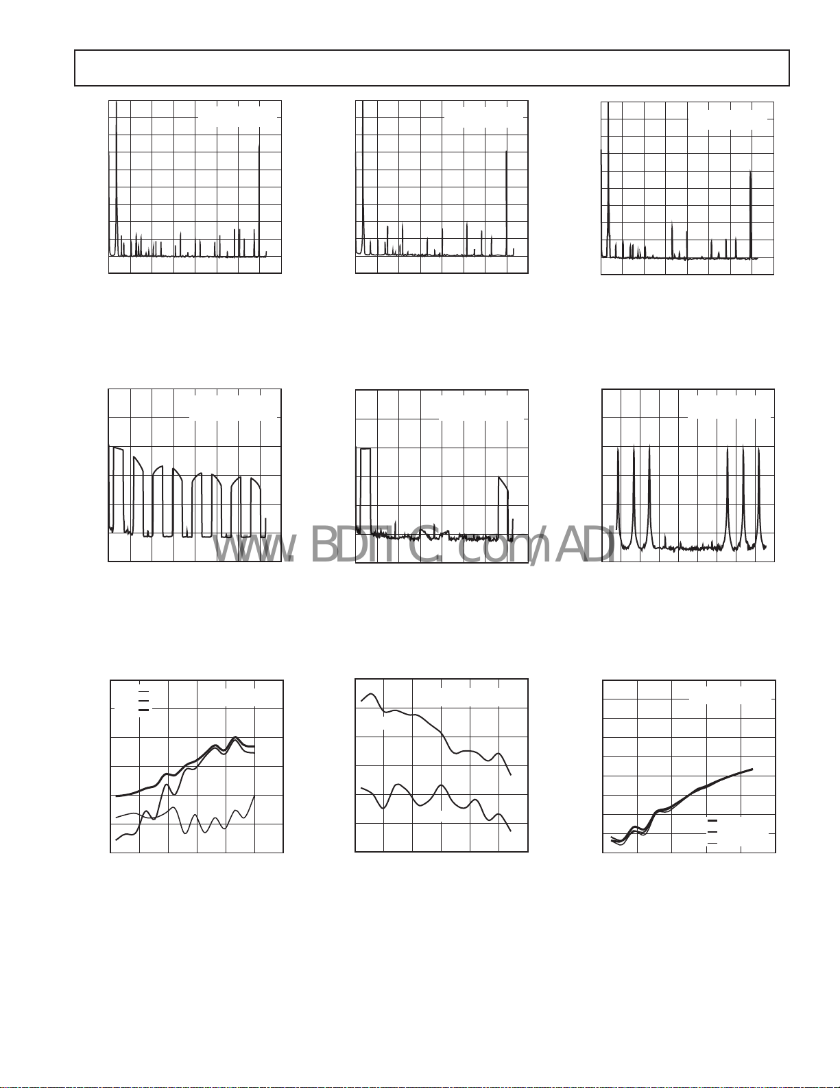
Typical Performance Characteristics–AD9860/AD9862
www.BDTIC.com/ADI
0
–10
–20
–30
–40
–50
–60
–70
MAGNITUDE – dBm
–80
–90
–100
0
20 40 60 80 100 110 120
FREQUENCY – MHz
f
= 32MSPS
DATA
4 INTERPOLATION
TPC 1. AD9862 Tx Output 6 MHz
Single Tone; CLKIN = 32 MHz;
0
Setting
f
= 32MSPS
DATA
1 INTERPOLATION
DLL 4
–20
–40
–60
140
0
–10
–20
–30
–40
–50
–60
–70
MAGNITUDE – dBm
–80
–90
–100
0
20 40
f
= 32MSPS
DATA
4 INTERPOLATION
80 100 110 120
60
FREQUENCY – MHz
TPC 2. AD9862 Tx Output 6 MHz
Single Tone; CLKIN = 64 MHz;
DLL 2 Setting
0
–20
–40
–60
f
= 32MSPS
DATA
4 INTERPOLATION
140
0
–10
–20
–30
–40
–50
–60
–70
MAGNITUDE – dBm
–80
–90
–100
0
20 40
FREQUENCY – MHz
f
DATA
4 INTERPOLATION
80 100 110 120
60
= 32MSPS
TPC 3. AD9862 Tx Output 6 MHz
Single Tone; CLKIN = 128 MHz;
DLL 1 Setting
0
–20
–40
–60
f
= 32MSPS
DATA
4 INTERPOLATION
140
–80
MAGNITUDE – dBm
–100
–120
0
20 40
60
80 100 110 120
FREQUENCY – MHz
140
TPC 4. TxDAC Generating an
OFDM Signal; CLKIN = 64 MHz,
DLL 2 Setting
–60
THD
2nd
3rd
–65
–70
–75
THD – dBc
–80
–85
–90
52035
10
f
= 64MSPS
DATA
2 INTERPOLATION
15 25 30
f
– MHz
OUT
TPC 7. TxDAC Harmonic
Distortion vs. f
OUT
–80
MAGNITUDE – dBm
–100
–120
0
20 40 60 80 100 110 120
FREQUENCY – MHz
140
TPC 5. TxDAC Generating an
OFDM Signal; CLKIN = 64 MHz,
DLL 2 Setting
74
73
72
71
SNR – dB
70
69
68
0
AD9862
5
f
= 64MSPS
DATA
2 INTERPOLATION
AD9860
10 15 25 30
FREQUENCY – MHz
20
TPC 8. Signal-to-Noise Ratio (SNR)
vs. f
OUT
–80
MAGNITUDE – dBm
–100
–120
7.90
7.92 7.94 7.96 7.98 8.00 8.02 8.04 8.06 8.08
FREQUENCY – MHz
TPC 6. Zoomed in Plot of Four
Notched Carriers of OFDM Signal;
CLKIN = 64 MHz, DLL 2 Setting
–50
–55
–60
–65
–70
–75
IMD – dBc
–80
–85
–90
–95
5
10 15 25 30
CARRIER FREQUENCY – MHz
f
= 64MSPS
DATA
2 INTERPOLATION
AV DD = 3.0V
AV DD = 3.3V
AV DD = 3.6V
20
TPC 9. Two Tone Intermodulation
vs. f
OUT1 (fOUT2
= f
+ 1 MHz)
OUT1
REV. 0
–9–
AD9860/AD9862
www.BDTIC.com/ADI
0
–20
–40
–60
–80
FFT MAGNITUDE – dBFS
–100
–120
0
10 15 25 30
5
FFT OUTPUT – MHz
20
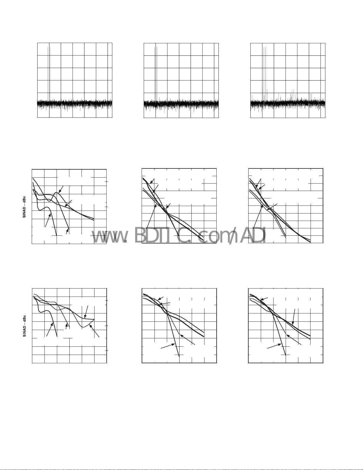
TPC 10. ADC Dual Tone FFT with
Buffer Tones at 4.5 MHz and 5.5 MHz
68
66
64
62
60
58
56
54
52
50
0 20050
BUFFERED
2V INPUT,
1 GAIN
BUFFERED BYPASS
2V INPUT, 1 GAIN
BUFFERED BYPASS
1V INPUT, 2 GAIN
BUFFERED 1V
INPUT, 2 GAIN
150 250100
f
– MHz
IN
300
11.0
10.5
10.0
9.5
9.0
8.5
8.0
TPC 13. AD9862 Rx SINAD
at 64 MSPS
vs. f
IN
0
–20
–40
–60
–80
FFT MAGNITUDE – dBFS
–100
–120
0
10 15 25 30
5
FFT OUTPUT – MHz
20
TPC 11. ADC Dual Tone FFT without
Buffer Tones at 4.5 MHz and 5.5 MHz
70
LOW POWER MODE 1, BUFFER BYPASSED,
68
2V p-p INPUT, 1 RxPGA GAIN
66
64
62
60
58
SINAD – dBc
56
54
52
50
BUFFER BYPASSED, 2V p-p,
1 RxPGA GAIN
BUFFER ENABLED,
1V p-p INPUT,
2 RxPGA GAIN
0 20050
LOW POWER MODE 1, BUFFER
ENABLED, 1V p-p INPUT,
2 RxPGA GAIN
150 250100
f
– MHz
IN
300
TPC 14. AD9862 Rx SINAD
vs. f
at 32 MSPS
IN
0
–20
–40
–60
–80
FFT MAGNITUDE – dBFS
–100
–120
0
10 15 25 30
5
FFT OUTPUT – MHz
20
TPC 12. ADC Dual Tone FFT
(undersampling) without Buffer
Tones at 69.5 MHz and 70.5 MHz
70
LOW POWER MODE 2, BUFFER BYPASSED,
68
2V p-p INPUT, 1 RxPGA GAIN
66
64
62
60
58
SINAD – dBc
56
54
52
50
BUFFER BYPASSED, 2V p-p,
1 RxPGA GAIN
BUFFER ENABLED,
1V p-p INPUT,
2 RxPGA GAIN
0 20050
LOW POWER MODE 2, BUFFER
ENABLED, 1V p-p INPUT,
2 RxPGA GAIN
150 250100
f
– MHz
IN
TPC 15. AD9862 Rx SINAD
vs. f
at 16 MSPS
IN
300
62
60
58
56
54
52
50
48
46
44
0 20050
BUFFERED 2V
INPUT, 1 GAIN
BUFFERED BYPASS
1V INPUT, 2 GAIN
BUFFERED 1V
INPUT, 2 GAIN
BUFFERED BYPASS
2V INPUT, 1 GAIN
150 250100
f
– MHz
IN
TPC 16. AD9860 Rx SINAD
at 64 MSPS
vs. f
IN
300
10.0
9.5
9.0
8.5
8.0
7.5
7.0
62
LOW POWER MODE 1, BUFFER BYPASSED,
2V p-p INPUT, 1 RxPGA GAIN
60
58
56
54
52
SINAD – dBc
50
LOW POWER
48
MODE 1,
BUFFER ENABLED,
46
1V p-p INPUT,
2 RxPGA GAIN
44
0 20050
BUFFER BYPASSED, 2V p-p,
1 RxPGA GAIN
BUFFER ENABLED,
1V p-p INPUT,
2 RxPGA GAIN
150 250100
f
– MHz
IN
TPC 17. AD9860 Rx SINAD
at 32 MSPS
vs. f
IN
300
62
LOW POWER MODE 2, BUFFER BYPASSED,
2V p-p INPUT, 1 RxPGA GAIN
60
58
56
54
52
SINAD – dBc
50
LOW POWER
48
MODE 2,
BUFFER ENABLED,
46
1V p-p INPUT,
2 RxPGA GAIN
44
0 20050
BUFFER BYPASSED, 2V p-p,
1 RxPGA GAIN
BUFFER ENABLED,
1V p-p INPUT,
2 RxPGA GAIN
150 250100
f
– MHz
IN
TPC 18. AD9860 Rx SINAD
at 16 MSPS
vs. f
IN
300
REV. 0–10–
 Loading...