AD9860 and AD9862
AD9860 and AD9862
April 24, 2002
The World Leader in High-Performance Signal Processing Solutions

AD9860/2 MxFE
4
AD9860/2 MxFE
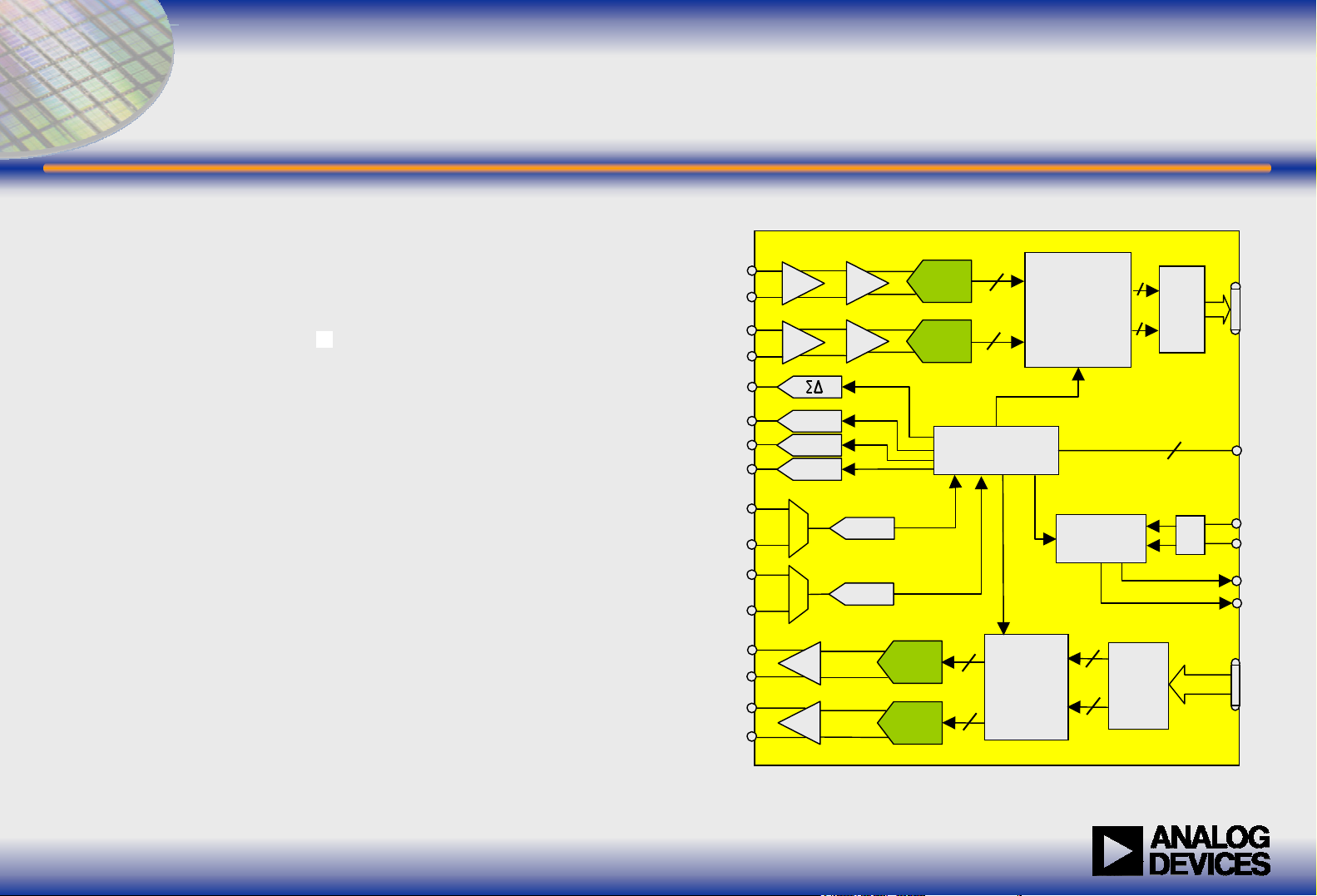
AD9860/2 FEATURES
TM
TM
for Broadband Communications
for Broadband Communications
A Versatile Mixed Signal Front-End Processor with Dual
Converter Receive and Dual Converter Transmit Paths
Receive path includes Dual 10-/12-Bit, 64 MSPS
Sampling A/D Converters with Internal or External
Independent References, Input Buffers, Programmable
Gain Amplifier (PGA), Low-Pass Decimation Filters
and a Digital Hilbert Block
Transmit path includes Dual 12-/14-bit, 128 MSPS
D/A Converters with Programmable Full Scale Output
Current, Channel independent Fine Gain and Offset
Control, Digital Hilbert and Interpolation Filters, Digital
Tunable Real or Complex Up-Converters
Internal Clock Distribution Block including a Delay-Locked
Loop based clock multiplier and Timing Generation
circuitry allow for single crystal or reference clock operation
Programmable Output Clocks, SPI compliant port, two
VIN+ A
VIN- B
VIN+ B
VIN- B
SIG DELTA
AUX_DAC_A
AUX_DAC_B
AUX_DAC_C
AUX_ADC_A
AUX_ADC_B
AUX_ADC_C
AUX_ADC_D
IOUT+ A
IOUT- A
IOUT+ B
IOUT- B
1X
1X
AUX DAC
AUX DAC
AUX DAC
PGA
PGA
PGA
PGA
AUX ADC
AUX ADC
DAC
DAC
ADC
ADC
SPI
REGISTERS
DIGITAL
PROCESSING
(BYPASSABLE)
HILBERT FILTER
MODULATION
DIGITAL
PROCESSING
(BYPASSABLE)
DECIMATION
HILBERT FILTER
DISTRIBUTION
+
+
+
CLOCK
LATCH
&
DEMUX
DATA
MUX
&
LATCH
DLL
RX DATA [0:
SERIAL PORT
OSC 1
OSC 2
CLKOUT1
CLKOUT2
TX DATA [0:1
Programmable Sigma Delta Outputs, four Auxiliary Analog
outputs and four Auxiliary ADC inputs
2
w w w . a n a l o g . c o m

AD9860/62 Dual Channel Mixed Signal
AD9860/62 Dual Channel Mixed Signal
Front End (
Front End (
Targeted at Broadband Wireless and other High Performance
Broadband Modem Applications
Dual 10/12-bit 64 MSPS ADC and Dual 12/14-bit 128MSPS DAC with 1X, 2X or 4X
Interpolation Integrated on a single IC
Tx Signal Path accepts and processes real or I&Q signals
Digital Hilbert filter facilitates an image rejection architecture when only
real data is available
Fs/4 and Fs/8 Digital Real or Complex Modulator
Fine Complex Modulator with a 24 bit controlled Numerically Controlled Oscillator
Supports Transmit LO suppression techniques with Independent Offset Control
and Single Sideband (SSB) architectures using Independent Fine Gain Control to
compensate for System offsets
MxFE))
MxFE
Rx Signal Path supports diversity or I&Q demodulation applications
Digital Decimation Filter can improve receive path performance
Hilbert Filter supports Receive Image Reject Architecture
Versatile Clock Interface, Low Phase Noise Internal DLL Clock Multiplier
Programmable registers accessed via SPI compliant Port
3
w w w . a n a l o g . c o m

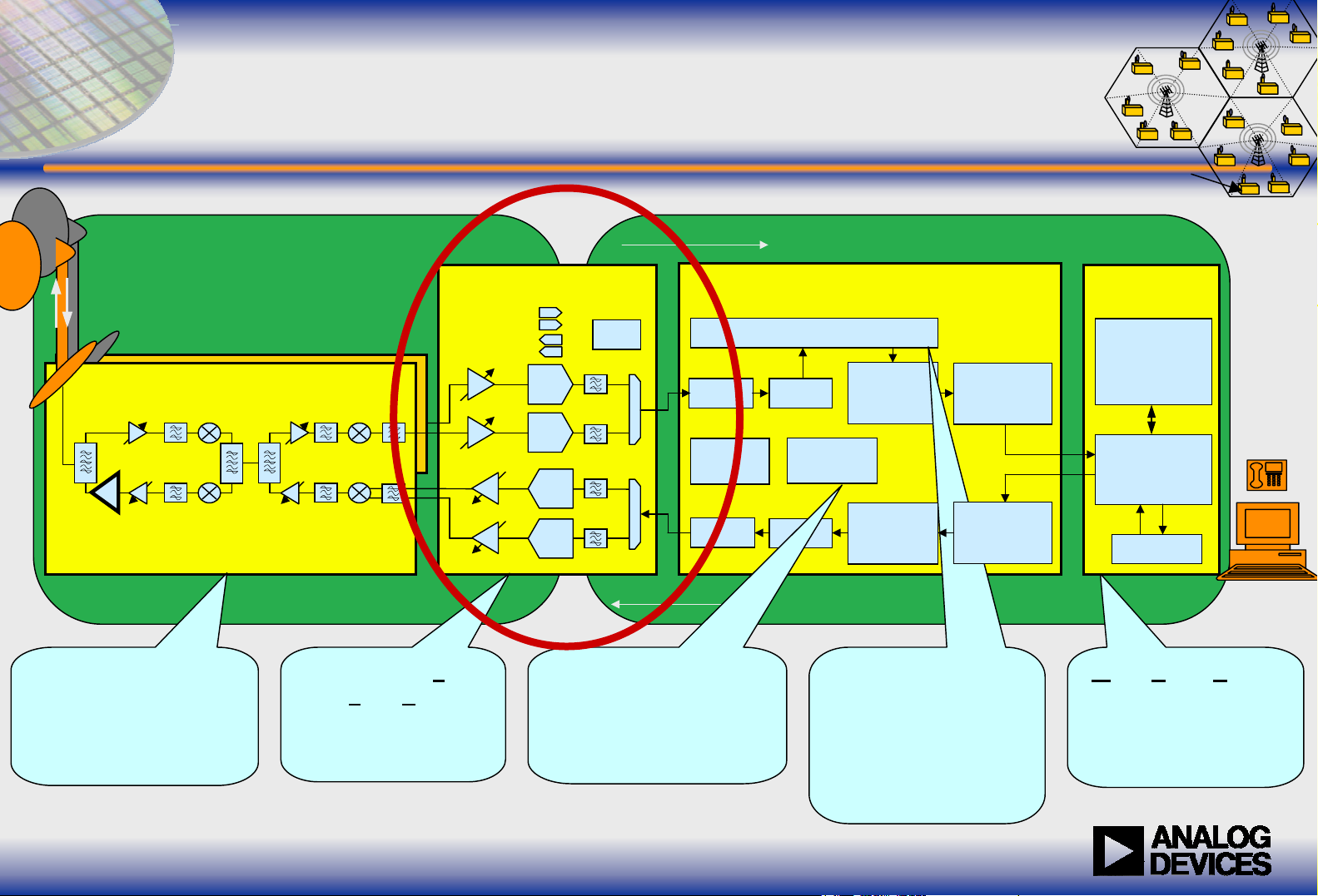
AD9862: Broadband Wireless Access Modem App.
AD9862: Broadband Wireless Access Modem App.
Antenna
Customer Premise Station
Linear Circuitry
2.5 - 2.68 GHz (MMDS)
3.5 GHz (Europe)
5.25 – 5.8 GHz (UNII)
RF / IF
RF / IF
up- / down converts
Baseband Signal
to / from RF frequencies
426 MHz
330 MHz
6-15 MHz BW
AD9862 Mixed Signal
Front End
ADCs, DACs
Signal Conditioning
MxFE
ADC
ADC
DAC
DAC
70 MBit/s max.
@15MHz BW
PLL
6 MBit/s max.
@15MHz BW
Modulator
Tone Mapper
QAM
OFDM
WCDMA
Digital Modem
Beam Former / Equalizer
Filter
Gain
Control
Filter
FFT
Timing
Recovery
IFFT
Complexity to handle high
channel at very high CNR:
complicated equalizer,
PHY
OFDM
QAM-
Decoder
OFDM
QAM-
Coder
Diversity Receive
frequency wireless
“beamforming”
Correction
Forward
Correction
Error
Error
MAC
MAC
RISC-
Processor
MAC
Hardware
Ethernet
10 MBit/s
Media Access Control
Channel Sharing
Address Filtering
Security
4
w w w . a n a l o g . c o m

AD9860/2
AD9860/2
MxFE
MxFE
TM
TM
Transmit Path
Transmit Path
IOUT+ A
IOUT- A
IOUT+ B
IOUT- B
Block A
PGA
PGA
DAC
DAC
Block B
Fs/4
Fs/8
Block C
Block D
Q
DDS
Block E
I
HILBERT
FILTER
DAC output of OFDM signal using various AD9862 digital processing features: 1.) 0 to 96 MHz spectrum
of “Real” output, 2.) with 4x Interpolation, Block C, 3.) with Fs/4 Up-conversion, Block B, 4.) with Hilbert
Filter, Block E, enabled 5.) Fine Tuned Modulation, Block D, enabled shifted by – 6MHz
Fig. 1
Fig. 2
Fig. 3
Fig. 4
Fig. 5
Block A
5
Block A+C
Block A+B+C
w w w . a n a l o g . c o m
Block A+B+C+E
Block A+B+C+D+E

Tx Path Image--
Tx Path Image
Rejection
Rejection
for Single or Multi--
for Single or Multi
Real, I/Q Single/Multi-Carrier, Interleaved
or Non- interleaved data
DSP or Customer
Digital ASIC
OSR X F
SYMBOL=FLO
4M
/(M*N)
FLO/N
AD9860/62
Interpolation
w/Fs/4 or Fs/8
Hilbert Filter +
Complex Modulation
Carrier Applications
Carrier Applications
F
/4
or F
DAC
DAC
F
/8
LO
0
AD8345/46/49
14-bit DAC
4N
14-bit DAC
LPF
LPF
x
0
90
x
Quadrature
Upconverter
Σ
FLO+F
or F
SAW
DAC
DAC
/4
/8
F
/4
or F
DAC
DAC
/8
0
6
w w w . a n a l o g . c o m
0

Tx Path Configured for
Tx Path Configured for
Image--
Image
Image of Signal
Rejection Applications
Rejection Applications
Desired Signal
LO
Feedthrough
7
w w w . a n a l o g . c o m

Simple Analog Interface Between
Simple Analog Interface Between
TxDAC’s
TxDAC’s
and ADI
and ADI
Quadrature
Quadrature
Modulators
Modulators
No Active DC Level Shifting Components Required!!!
~
~
V
DIFF
=1.0Vp-pand
VCM=0.7 V
AD9860/62
VPBF
12/14-bit DAC
ITxDAC
IOUTA
IOUTB
AD9860 or AD9862
QOUTA
12/14-bit DAC
QTxDAC
QOUTB
BBIP
BBIN
BBQP
BBQN
X
Phase
Splitter
X
VOUT
+
LOIP
LOIN
AD8345
~
~
8
w w w . a n a l o g . c o m
Differential
RLC Filter

Direct Conversion Possible Using AD8349
Direct Conversion Possible Using AD8349
Single Carrier
WCDMA
67 dB ACLR
Quadrature
Quadrature
Modulator
Modulator
9
w w w . a n a l o g . c o m

AD9860/2
AD9860/2
MxFE
MxFE
TM
TM
Receive Path
Receive Path
Vin+ A
Vin- A
Vin+ B
VinT- B
PGA
PGA
ADC
ADC
Rx without Decimation
SINAD 64.6dBFS
THD –70.07 dBFS
Distorted input – 12.5MHz
Single tone
HILBERT
FILTER
Rx with Decimation
SINAD 66.8 dBFS
THD –84.5 dBFS
10
w w w . a n a l o g . c o m

Supports
Supports
Down Conversion Receive Architectures
Down Conversion Receive Architectures
Quadrature
Down
Converter
Baseband
Baseband
I/Q or Image Rejection
I/Q or Image Rejection
Mixed Signal Front End (MxFE)
AD8347
+
AD9860/62
(t)
I
LPF
X
0
90
X
LO
(t)
Q
LPF
LPF
LPF
1X
F
c
1X
PGA
PGA
ADC
DECIMATION
+
HILBERT FILTER
ADC
11
w w w . a n a l o g . c o m

Dual Channel Direct IF Receive
Dual Channel Direct IF Receive
Architecture
Architecture
AD9860/62
12
FILTER
& LNA
FILTER
& LNA
X
LO
X
LO
FILTER
FILTER
ADC
FS
ADC
w w w . a n a l o g . c o m
DSP or
ASIC
DSP or
ASIC
 Loading...