1 GSPS
FEATURES
1 GSPS internal clock speed
Up to 2 GHz input clock (selectable divide-by-2)
Integrated 10-bit D/A converter
Phase noise < 145 dBc/Hz @ 1 kHz offset
Output frequency = 100 MHz (DAC output)
32-bit programmable frequency register
Simplified 8-bit parallel and SPI® serial control interface
Automatic frequency sweeping capability
4 frequency profiles
3.3 V power supply
Power dissipation 2 W typical
Integrated programmable charge pump and phase
frequency detector with fast lock circuit
Isolated charge pump supply up to 5 V
Integrated 2 GHz mixer
APPLICATIONS
VHF/UHF LO synthesis
Tuners
Instrumentation
Agile clock synthesis
Cellular base station hopping synthesizer
Radar
Sonet/SDH clock synthesis
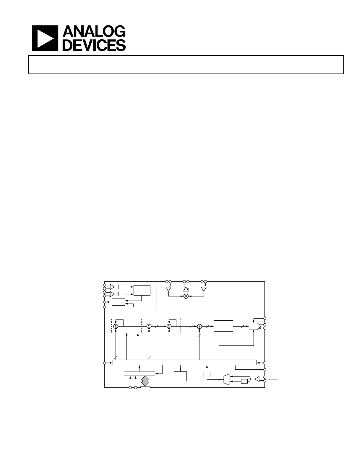
FUNCTIONAL BLOCK DIAGRAM
LO IF RF
DIV
PD
CP
CPISET
RESET
Rev. A
Information furnished by Analog Devices is believed to be accurate and reliable.
However, no responsibility is assumed by Analog Devices for its use, nor for any
infringements of patents or other rights of third parties that may result from its use.
Specifications subject to change without notice. No license is granted by implication
or otherwise under any patent or patent rights of Analog Devices. Trademarks and
registered trademarks are the property of their respective owners.
CHARGE
PUMP
FREQUENCY
ACCUMULATOR
WORD
DELTA
FREQUENCY
32
÷ M
÷ N
PHASE
DETECTOR
DIGITAL PLL
DELTA
RESET
RAMP RATE
FREQUENCY
FREQUENCY
ACCUMULATOR
CONTROL REGISTERS
PROFILE
SELECT
WORD
TUNING
FREQUENCY
32
I/O PORT
(SER/PAR)
PHASE
ACCUMULATOR
32
RESET
PHASE
ACCUMULATOR
TIMING AND CONTROL LOGIC
SYNC
ANALOG
MULTIPLIER
POWER-
DOWN
LOGIC
Figure 1.
Direct Digital Synthesizer
AD9858
GENERAL DESCRIPTION
The AD9858 is a direct digital synthesizer (DDS) featuring a
10-bit DAC operating up to 1GSPS. The AD9858 uses advanced
DDS technology, coupled with an internal high speed, high
performance D/A converter to form a digitally programmable,
complete high frequency synthesizer capable of generating a
frequency-agile analog output sine wave at up to 400+ MHz.
The AD9858 is designed to provide fast frequency hopping and
fine tuning resolution (32-bit frequency tuning word). The
frequency tuning and control words are loaded into the AD9858
via parallel (8-bit) or serial loading formats. The AD9858
contains an integrated charge pump (CP) and phase frequency
detector (PFD) for synthesis applications requiring the
combination of a high speed DDS along with phase-locked loop
(PLL) functions. An analog mixer is also provided on-chip for
applications requiring the combination of a DDS, PLL, and
mixer, such as frequency translation loops, tuners, and so on.
The AD9858 also features a divide-by-2 on the clock input,
allowing the external clock to be as high as 2 GHz.
The AD9858 is specified to operate over the extended industrial
temperature range of –40°C to +85°C.
AD9858
15
PHASE
OFFSET
ADJUST
PHASE-TO-
15 10
AMPLITUDE
CONVERSION
14
DAC CLOCK
÷ 8
M
U
X
÷ 2
One Technology Way, P.O. Box 9106, Norwood, MA 02062-9106, U.S.A.
Tel: 781.329.4700
Fax: 781.326.8703 © 2003 Analog Devices, Inc. All rights reserved.
www.analog.com
DAC
DACISET
I
OUT
I
OUT
FUD
SYNCLK
REFCLK
REFCLK
03166-A-001

AD9858
TABLE OF CONTENTS
Features .......................................................................................... 1
Overview ..................................................................................... 15
Applications................................................................................... 1
General Description..................................................................... 1
Functional Block Diagram .......................................................... 1
AD9858—Electrical Specifications ................................................ 3
Absolute Maximum Ratings............................................................ 6
ESD Caution.................................................................................. 6
Pin Configuration............................................................................. 7
Pin Function Descriptions .............................................................. 8
Typical Performance Characteristics ........................................... 10
Theory of Operation ...................................................................... 15
REVISION HISTORY
11/03—Data Sheet Changed from a REV. 0 to a REV. A
Changes to SPECIFICATIONS........................................................ 5
Moved ESD Caution to ..................................................................... 6
Component Blocks..................................................................... 15
Modes of Operation ................................................................... 17
Synchronization.......................................................................... 19
Programming the AD9858........................................................ 21
AD9858 Application Suggestions............................................. 29
Evaluation Boards ...................................................................... 30
Outline Dimensions....................................................................... 31
Wa r ni n g ....................................................................................... 31
Ordering Guide .......................................................................... 31
Moved Pin Configuration to............................................................ 7
Moved Pin Function Description to ............................................... 8
Changes to Equations........................................................................ 19
Changes to Delta Frequency Ramp Rate Word (DFRRW).......... 27
Rev. A | Page 2 of 32

AD9858
AD9858—ELECTRICAL SPECIFICATIONS
Table 1. Unless otherwise noted, VDD = 3.3 V ± 5%, CPVDD = 5 V ± 5%, R
Reference Clock Frequency = 1 GHz.
Parameter Temp Test Level Min Typ Max Unit
REF CLOCK INPUT CHARACTERISTICS
1, 2
Reference Clock Frequency Range (Divider Off) Full VI 10 1000 MHz
Reference Clock Frequency Range (Divider On) Full VI 20 2000 MHz
Duty Cycle @ 1 GHz 25°C V 42 50 58 %
Input Capacitance 25°C V 3 pF
Input Impedance 25°C IV 1500 Ω
Input Sensitivity Full VI –20 +5 dBm
DAC OUTPUT CHARACTERISTICS
Resolution Full 10 Bits
Full-Scale Output Current Full 5 20 40 mA
Gain Error Full VI –10 +10 % FS
Output Offset Full VI 15 µA
Differential Nonlinearity Full VI 0.5 1 LSB
Integral Nonlinearity Full VI 1 1.5 LSB
Output Impedance Full VI 100 kΩ
Voltage Compliance Range Full VI AVDD – 1.5 AVDD + 0.5 V
Wideband SFDR (DC to Nyquist)
40 MHz F
100 MHz F
180 MHz F
360 MHz F
180 MHz F
Full V 60 dBc
OUT
Full V 54 dBc
OUT
Full V 53 dBc
OUT
Full V 50 dBc
OUT
(700 MHz REFCLK) Full IV 52 dBc
OUT
Narrow-Band SFDR33
40 MHz F
40 MHz F
40 MHz F
100 MHz F
100 MHz F
100 MHz F
180 MHz F
180 MHz F
180 MHz F
360 MHz F
360 MHz F
360 MHz F
180 MHz F
180 MHz F
180 MHz F
OUTPUT PHASE NOISE CHARACTERISTICS (@ 103 MHz I
(±15 MHz) Full V 82 dBc
OUT
(±1 MHz) Full V 87 dBc
OUT
(±50 kHz) Full V 88 dBc
OUT
(±15 MHz) Full V 81 dBc
OUT
(±1 MHz) Full V 82 dBc
OUT
(±50 kHz) Full V 86 dBc
OUT
(±15 MHz) Full V 74 dBc
OUT
(±1 MHz) Full V 84 dBc
OUT
(±50 kHz) Full V 85 dBc
OUT
(±15 MHz) Full V 75 dBc
OUT
(±1 MHz) Full V 85 dBc
OUT
(±50 kHz) Full V 86 dBc
OUT
(±15 MHz) (700 MHz REFCLK) Full V 65 dBc
OUT
(±1 MHz) (700 MHz REFCLK) Full V 80 dBc
OUT
(±50 kHz) (700 MHz REFCLK) Full V 84 dBc
OUT
)
OUT
@ 1 kHz Offset Full V –147 dBc/Hz
@ 10 kHz Offset Full V –150 dBc/Hz
@ 100 kHz Offset Full V –152 dBc/Hz
OUTPUT PHASE NOISE CHARACTERISTICS (@ 403 MHz I
)
OUT
@ 1 kHz Offset Full V –133 dBc/Hz
@ 10 kHz Offset Full V –137 dBc/Hz
@ 100 kHz Offset Full V –140 dBc/Hz
= 2 kΩ, C
SET
= 2.4 kΩ,
PISET
Rev. A | Page 3 of 32

AD9858
Parameter Temp Test
Level
OUTPUT PHASE NOISE CHARACTERISTICS (@ 100 MHz I
OUT
with 700 MHz REFCLK)
@ 100 Hz Offset Full V –125 dBc/Hz
@ 1 kHz Offset Full V –140 dBc/Hz
@ 10 kHz Offset Full V –148 dBc/Hz
@ 100 kHz Offset Full V –150 dBc/Hz
@ 1 MHz Offset Full V –150 dBc/Hz
@ 10 MHz Offset Full V –150 dBc/Hz
PHASE DETECTOR AND CHARGE PUMP
Phase Detector Frequency Full VI 150 MHz
Phase Detector Frequency (Divide-by-4 Enabled)4 Full VI 400 MHz
Charge Pump Sink and Source Current5 Full VI 4 mA
Fast Lock Current (Acquisition Only) Full VI 7 mA
Open-Loop Current (Acquisition Only) Full VI 30 mA
Sink and Source Current Absolute Accuracy6 Full V 2.5 %
Sink and Source Current Matching6 Full V 1 %
Input Sensitivity PDIN and DIVIN (50 Ω)7 Full IV –15 0 dBm
Input Impedence PDIN and DIVIN (Single-Ended) Full V 1 kΩ
Phase Noise @ 100 MHz Input Frequency
@ 10 kHz Offset Full V 110 dBc/Hz
@ 100 kHz Offset Full V 140 dBc/Hz
@ 1 MHz Offset Full V 148 dBc/Hz
Charge Pump Output Range8 Full V CPVDD V
MIXER
9
IF
Full V 400 MHz
OUT
FRF Full VI 2 GHz
FLO Full VI 2 GHz
Conversion Gain Full VI 0.0 3.5 dB
LO Level Full VI –10 +5 dBm
RF Level Full VI –20 dBm
Input IP3 Full VI 5 9 dBm
1 dB Input Compression Power10 Full VI –3 dBm
Input Impedance (Single-Ended)
LO Full V 1 kΩ
RF Full V 1 kΩ
LOGIC INPUTS
Logic 1 Voltage Full VI 2.0 V
Logic 0 Voltage Full VI 0.8 V
Logic 1 Current Full VI 12 µA
Logic 0 Current Full VI 12 µA
Input Capacitance Full V 3 pF
POWER SUPPLY
P
(Worst-Case Conditions—Everything on
DISS
P
Input Frequency 150 MHz)
FD
P
(DAC and DDS Core Only Worst-Case) Full VI 1.7 2 W
DISS
P
(Power-Down Mode) Full VI 65 100 mW
DISS
P
Mixer Only Full VI 60 75 mW
DISS
P
PFD and CP (@ 100 MHz) Only Full VI 350 435 mW
DISS
Full VI 2 2.5 W
Min Typ Max Unit
Rev. A | Page 4 of 32
AD9858
Parameter Temp Test
Level
TIMING CHARACTERISTICS
Serial Control Bus
Maximum Frequency Full IV 10 MHz
Minimum Clock Pulse Width Low (t
Minimum Clock Pulse Width High (t
) Full IV 5.5 ns
PWL
) Full IV 15 ns
PWH
Maximum Clock Rise/Fall Time Full IV 1 ms
Minimum Data Setup Time (tDS) Full IV 7 ns
Mimimum Data Hold Time (tDH) Full IV 0 ns
Maximum Data Valid Time (tDV) Full IV 20 ns
Parallel Control Bus
WR Minimum Low Time
WR Minimum High Time
WR Minimum Period
Address to WR Setup (T
Address to WR Setup (T
Data to WR Setup (T
Data to WR Hold (T
DHU
DSU
)
)
ASU
AHU
)
)
Full IV 3 ns
Full IV 6 ns
Full IV 9 ns
Full IV 3 ns
Full IV 0 ns
Full IV 3.5 ns
Full IV 0 ns
Miscellaneous Timing Specifications
REFCLK to SYNCLK Full V 2.5 ns
FUD to SYNCLK Setup Time Full IV 4 ns
FUD to SYNCLK Hold Time Full IV 0 ns
REFCLK to SYNCLK Delay Full IV 2.5 3 ns
FUD Rising Edge to Frequency Change
Single Tone Mode 25°C IV 83
Linear Sweep Mode 25°C IV 99
FUD Rising Edge to Phase Offset Change 25°C IV 83
Min Typ Max Unit
sysclk
cycles
sysclk
cycles
sysclk
cycles
1
The reference clock input is configured to accept a differential or single-ended sine wave input or a 3 V CMOS-level pulse input.
2
REFCLK input is internally dc biased. AC coupling should be used.
3
Reference clock frequency is selected to ensure second harmonic is out of the bandwidth of interest.
4
PD inputs sent @ 400 MHz, with divide-by-4 enabled.
5
The charge pump current is programmable in eight discrete steps, minimum value assumes current sharing.
6
For 0.75 V < VCP < CPVDD – 0.75 V.
7
These differential inputs are internally dc biased. AC coupling should be used.
8
The charge pump supply voltage can range from 4.75 V to 5.25 V.
9
Output interface is differential open collector.
10
For 1 dB output compression; input power measured at 50 Ω.
Rev. A | Page 5 of 32
AD9858
ABSOLUTE MAXIMUM RATINGS
Table 2.
Parameter Rating
AVDD 4 V
DVDD 4 V
CPVDD 6 V
Digital Input Voltage –0.7 V to +VDD
Digital Output Current 5 mA
Storage Temperature –65°C to +150°C
Operating Temperature –40°C to +85°C
θJA EPAD Soldered 25°C/W
Table 3. Explanation of Test Levels
I 100% Production Tested.
III Sample Tested Only.
IV
Parameter is guaranteed by design and characterization
testing.
V Parameter is a typical value only.
VI
Devices are 100% production tested at 25°C and
guaranteed by design and characterization testing for
industrial operating temperature range.
Absolute Maximum Ratings are limiting values, to be applied
individually, and beyond which the serviceability of the circuit
may be impaired. Functional operability under any of these
conditions is not necessarily implied. Exposure of absolute
maximum rating conditions for extended periods of time may
affect device reliability.
ESD CAUTION
ESD (electrostatic discharge) sensitive device. Electrostatic charges as high as 4000 V readily accumulate on the
human body and test equipment and can discharge without detection. Although this product features
proprietary ESD protection circuitry, permanent damage may occur on devices subjected to high energy
electrostatic discharges. Therefore, proper ESD precautions are recommended to avoid performance
degradation or loss of functionality.
Rev. A | Page 6 of 32
AD9858
T
A
T
PIN CONFIGURATION
AGND
PS1
SYNCLK
FUD
100999897
PS0
DGND
DGND
DVDD
96
95
DVDD
949392 91 90 89 88
RESET
AVDD
SPSELEC
AVDD
AVDD
AGND
87 86 85
IOUT
AGND
84
IOUT
IOUT
83 82 81 80 79 78 77 76
IOUT
AGND
DACISET
AVDD
DACBP
NC
DGND
DGND
DVDD
DVDD
ADDR5
ADDR4
ADDR3
DDR2/IORESE
ADDR1/SDO
ADDR0/SDIO
WR/SCLK
DVDD
DGND
RD/CS
DVDD
DVDD
DVDD
D7
1
D6
2
D5
3
D4
4
5
6
7
8
D3
9
D2
10
D1
11
D0
12
13
14
15
16
17
18
19
20
21
22
23
24
13
25
AD9858
TOP VIEW
(Not to Scale)
75
74
73
72
71
70
69
68
67
66
65
64
63
62
61
60
59
58
57
56
55
54
53
52
51
NC
AGND
AVDD
DIV
DIV
AVDD
AGND
CPGND
CPVDD
CP
CP
CPFL
CPGND
CPVDD
CPISET
NC
NC
PFD
PFD
IF
IF
RF
RF
AGND
AVDD
27
26 28
DVDD
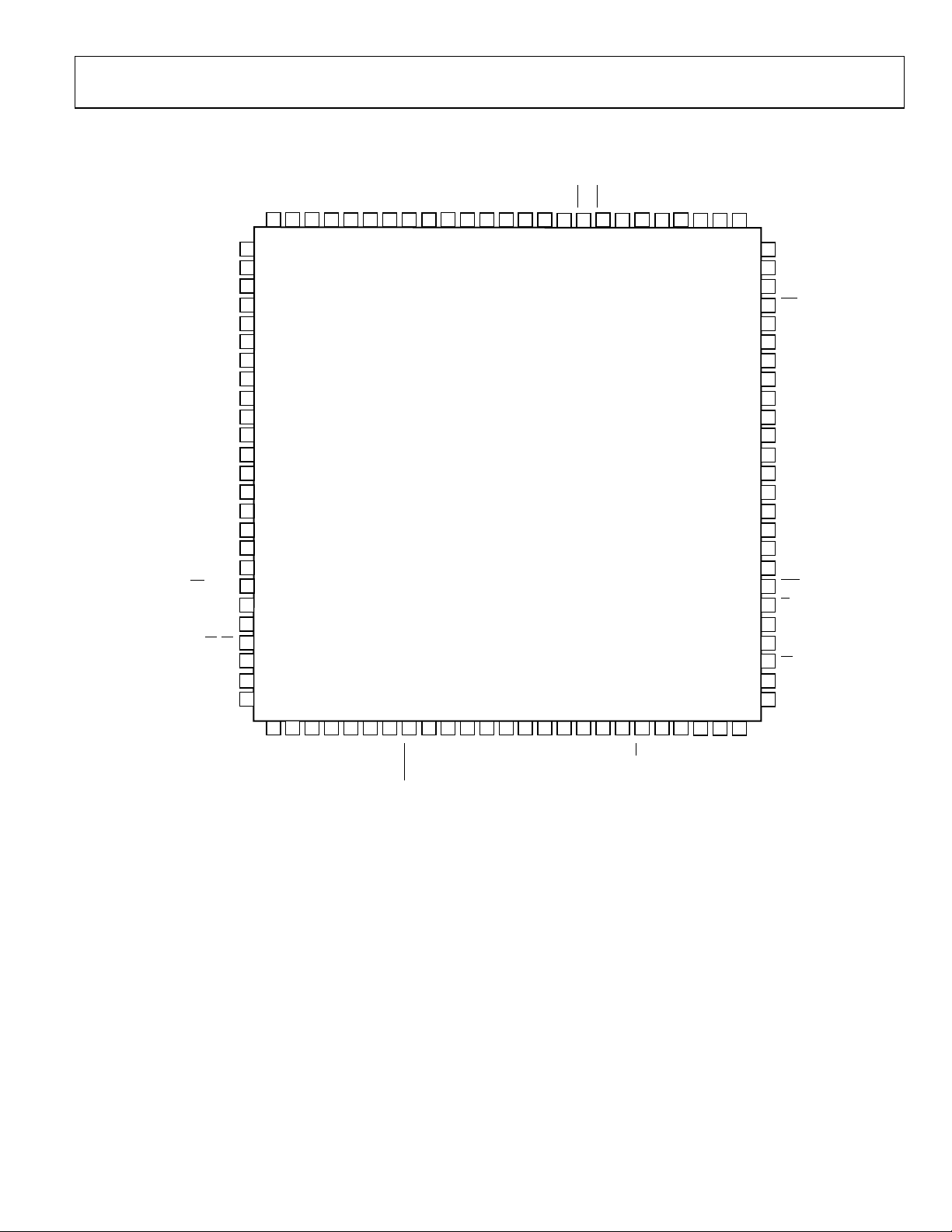
NC = NO CONNECT
DVDD
29
DGND
30
AGND
313233
AVDD
AGND
AVDD
REFCLK
343536 37
AVDD
AVDD
REFCLK
38
AGND
39
AGND
AGND
42
41
40
AVDD
4344454647 48 49 50
LO
LO
AVDD
AVDD
AGND
AGND
AVDD
AVDD
AGND
AGND
66-A-044
031
Figure 2. 100-Lead EPAD (SV-100) Pin Configuration
Rev. A | Page 7 of 32
AD9858
PIN FUNCTION DESCRIPTIONS
Table 4. Pin Function Descriptions—100-Lead EPAD (SV-100)
Pin No. Mnemonic I/O Description
1 to 4, 9 to 12 D7 to D0 I
5, 6, 21, 28, 95, 96 DGND Digitial Ground.
7, 8, 20,
23 to 27, 93, 94
13 to 18
16 IORESET I
17 SDO O
18 SDIO
19
22
29, 30, 37 to 39,
41, 42, 49, 50,
52, 69, 74, 80, 85,
87, 88
31, 32, 35, 36,
40, 43, 44, 47,
48, 51, 70, 73,
77, 86, 89, 90
33
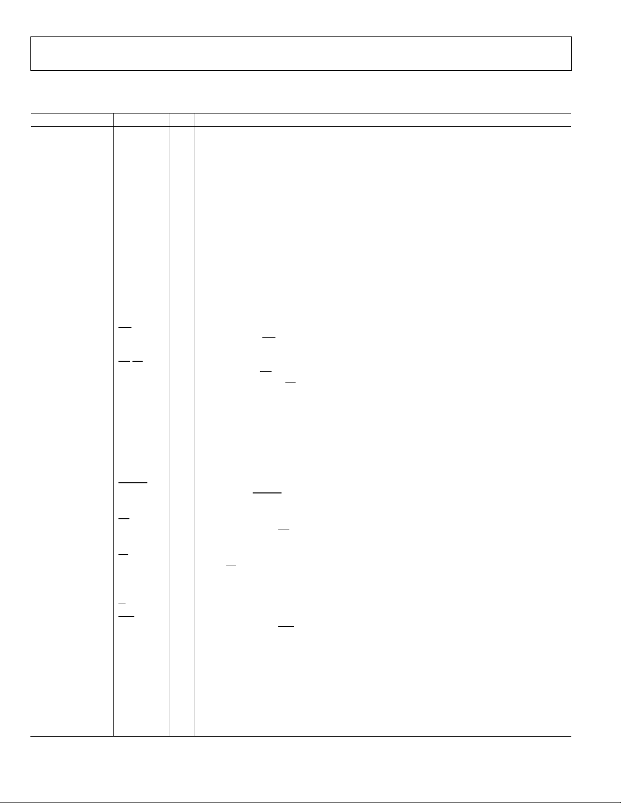
34 REFCLK I Reference Clock Input.
45
46 LO I Mixer Local Oscillator (LO) Input.
53
54 RF I Analog Mixer RF Input.
55 IF O Analog Mixer IF Output.
56
57
58 PFD I Phase Frequency Detector Input.
59, 60, 75, 76 NC No Connection.
61 CPISET I
62, 67 CPVDD I Charge Pump Supply Voltage.
63, 68 CPGND I Charge Pump Ground.
64 CPFL O Charge Pump Fast Lock Output.
65, 66 CP O Charge Pump Output.
DVDD Digital Supply Voltage.
ADDR5 to
ADDR0
WR/SCLK
RD/CS
AGND I Analog Ground.
AVDD I Analog Supply Voltage.
REFCLK
LO
RF
IF
PFD
Parallel Port DATA. Note that the functionality of these pins is valid only when the I/O port is
configured as a parallel port.
I
When the I/O port is configured as a parallel port, these pins serve as a 6-bit address select
for accessing the on-chip registers (see the IORESET, SDO, and SDIO pins below for serial
port mode).
Note that this is valid only for serial programming mode. Active high input signal that resets the
serial I/O bus controller. It is intended to serve as a means of recovering from an unresponsive
serial bus caused by improper programming protocol. Asserting an I/O reset does not affect the
contents of previously programmed registers nor does it invoke their default values.
Note that this is valid only for serial programming mode. When operating the I/O port as a
3-wire serial port, this pin serves as a unidirectional serial data output pin. When operated as a
2-wire serial port, this pin is unused.
I or
Note that this is valid only for serial programming mode. When operating the I/O port as a
I/O
3-wire serial port, this pin is the serial data input. When operated as a 2-wire serial port, this pin
is the bidirectional serial data pin.
I
When the I/O port is configured for parallel programming mode, this pin functions as an active
low write pulse (
serial data clock (SCLK).
I
When the I/O port is configured for parallel programming mode, this pin functions as an active
low read pulse (RD). When configured for serial programming mode, this pin functions as an
active low chip select (
I
Reference Clock Complementary Input. (Note that when the REFCLK port is operated in singleended mode,
I
Mixer Local Oscillator (LO) Complementary Input. Note that when the LO port is operated in
single-ended mode,
I
Analog Mixer RF Complementary Input. Note that when the RF port is operated in single-ended
RF should be decoupled to AVDD with a 0.1 µF capacitor.
mode,
O Analog Mixer IF Complementary Output.
I
Phase Frequency Detector Complementary Input . Note that when the PFD port is operated in
single-ended mode,
Charge Pump Output Current Control. A resistor connected from CPISET to CPGND establishes
the reference current for the charge pump.
WR). When configured for serial programming mode, this pin functions as the
CS) that allows multiple devices to share the serial bus.
REFCLK should be decoupled to AVDD with a 0.1 µF capacitor.
LO should be decoupled to AVDD with a 0.1 µF capacitor.
PFD should be decoupled to AVDD with a 0.1 µF capacitor.
Rev. A | Page 8 of 32

AD9858
Pin No. Mnemonic I/O Description
71 DIV I Phase Frequency Detector Feedback Input.
72
78 DACBP DAC Baseline Decoupling Pin, Typically Bypassed to Pin 77 with a 0.1 µF Capacitor.
79 DACISET I A Resistor Connected from DACISET to AGND Establishes the Reference Current for the DAC.
81, 82 IOUT O DAC Output.
83, 84
91 SPSELECT I
92 RESET I
97, 98 PS0, PS1 I
99 FUD I
100 SYNCLK O Clock Output Pin that Serves as a Synchronizer for External Hardware. SYNCLK runs at REFCLK/8.
DIV
IOUT
I
Phase Frequency Detector Feedback Complementary Input. Note that when the DIV port is
operated in single-ended mode,
O DAC Complementary Output.
I/O Port Serial/Parallel Programming Mode Select Pin. Logic 0: serial programming mode.
Logic 1: parallel programming mode.
Active High Hardware Reset Pin. Assertion of the RESET pin forces the AD9858 to its default
operating conditions.
Used to Select One of the Four Internal Profiles. These pins are synchronous to the
SYNCLK output.
Frequency Update. The rising edge transfers the contents of the internal buffer registers to the
memory registers. This pin is synchronous to the SYNCLK output.
DIV should be decoupled to AVDD with a 0.1 µF capacitor.
Rev. A | Page 9 of 32
AD9858
–
–
–
–
–
–
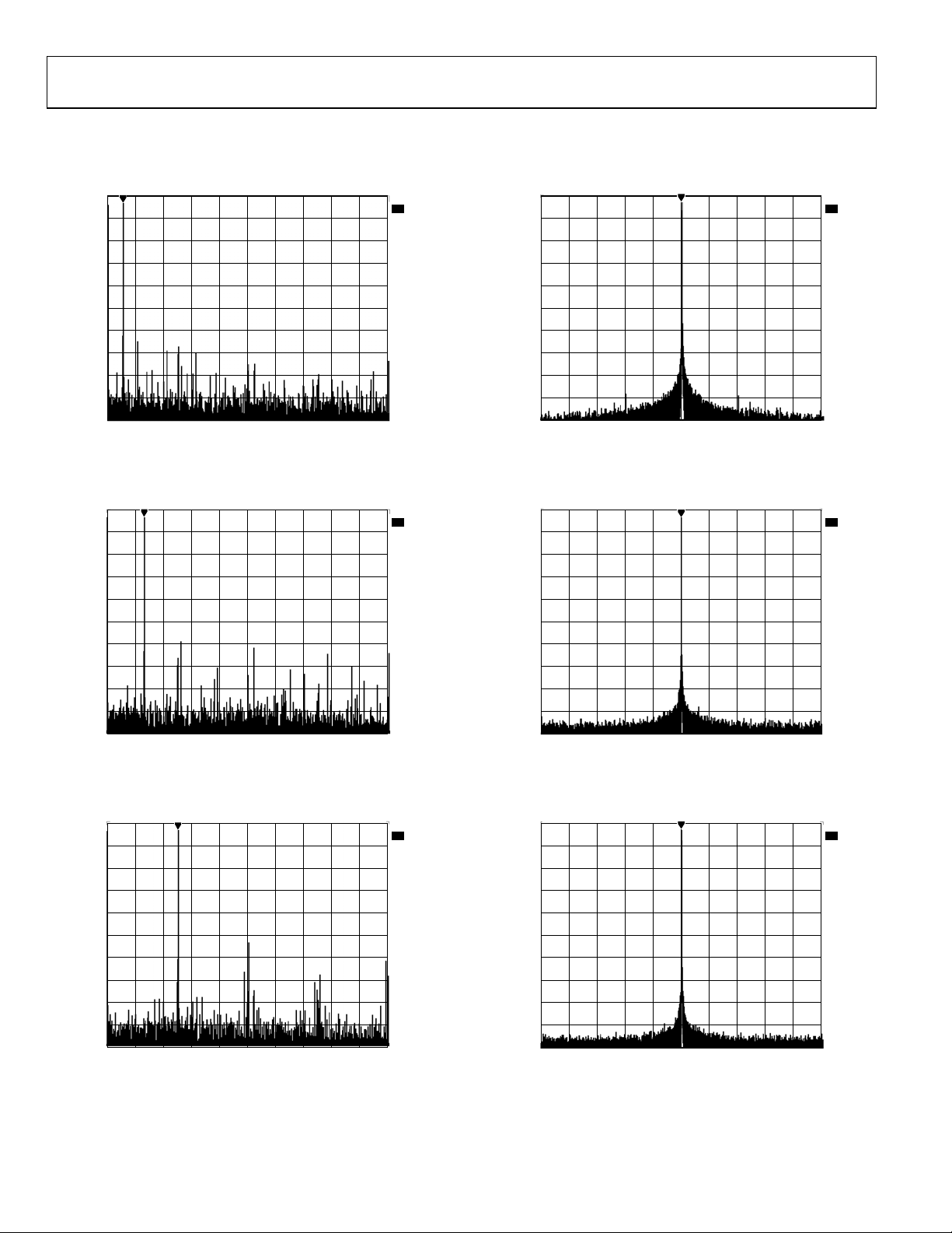
TYPICAL PERFORMANCE CHARACTERISTICS
1.04dBm
1.72dBm
1.39dBm
RBW
VBW
SWT
RBW
VBW
SWT
RBW
VBW
SWT
5kHz
5kHz
50s
5kHz
5kHz
50s
5kHz
5kHz
50s
RF ATT
UNIT
OUT
RF ATT
UNIT
OUT
RF ATT
UNIT
OUT
20dB
dB
A
1AP
03166-A-002
20dB
dB
A
1AP
03166-A-003
20dB
dB
A
1AP
03166-A-004
1
MARKER 1 [T1]
26.05210421MHz
REF LVL
0
5dBm
–10
–20
–30
–40
–50
–60
–70
–80
–90
100
START 0Hz 50MHz/ STOP 500MHz
Figure 3. Wideband SFDR, 26 MHz F
REF LVL
5dBm
0
–10
–20
–30
–40
–50
–60
–70
–80
–90
100
START 0Hz 50MHz/ STOP 500MHz
MARKER 1 [T1]
1
65.13026052MHz
Figure 4. Wideband SFDR, 65 MHz F
REF LVL
5dBm
0
–10
–20
–30
–40
–50
–60
–70
–80
–90
100
START 0Hz 50MHz/ STOP 500MHz
MARKER 1 [T1]
126.25250501MHz
1
Figure 5. Wideband SFDR, 126 MHz F
REF LVL
0
5dBm
MARKER 1 [T1]
26.10050100MHz
1.73dBm
RBW
200Hz
200Hz
64s
RF ATT
UNIT
VBW
SWT
1
–10
–20
–30
–40
–50
–60
–70
–80
–90
100
CENTER 26.1MHz 50kHz/ SPAN 500kHz
500Hz
500Hz
40s
OUT
, 1 MHz BW
RF ATT
UNIT
Figure 6. Narrow-Band SFDR, 26 MHz F
REF LVL
0
5dBm
MARKER 1 [T1]
65.10200401MHz
1.58dBm
RBW
VBW
SWT
1
–10
–20
–30
–40
–50
–60
–70
–80
–90
100
CENTER 65.1MHz 200kHz/ SPAN 2MHz
500Hz
500Hz
40s
OUT
, 1 MHz BW
RF ATT
UNIT
Figure 7. Narrow-Band SFDR, 65 MHz F
REF LVL
0
5dBm
MARKER 1 [T1]
126.10200401MHz
1.27dBm
RBW
VBW
SWT
1
–10
–20
–30
–40
–50
–60
–70
–80
–90
100
CENTER 126.1MHz 200kHz/ SPAN 2MHz
Figure 8. Narrow-Band SFDR, 126 MHz F
, 1 MHz BW
OUT
20dB
dB
A
1AP
03166-A-006
20dB
dB
A
1AP
03166-A-007
20dB
dB
A
1AP
03166-A-008
Rev. A | Page 10 of 32
 Loading...