REV. B
Information furnished by Analog Devices is believed to be accurate and
reliable. However, no responsibility is assumed by Analog Devices for its
use, nor for any infringements of patents or other rights of third parties that
may result from its use. No license is granted by implication or otherwise
under any patent or patent rights of Analog Devices.
a
AD9857
One Technology Way, P.O. Box 9106, Norwood, MA 02062-9106, U.S.A.
Tel: 781/329-4700 www.analog.com
Fax: 781/326-8703 © Analog Devices, Inc., 2002
CMOS 200 MSPS 14-Bit
Quadrature Digital Upconverter
FEATURES
200 MHz Internal Clock Rate
14-Bit Data Path
Excellent Dynamic Performance
80 dB SFDR @ 65 MHz (ⴞ100 kHz) A
OUT
4ⴛ–20ⴛ Programmable Reference Clock Multiplier
Reference Clock Multiplier PLL Lock Detect Indicator
Internal 32-Bit Quadrature DDS
FSK Capability
8-Bit Output Amplitude Control
Single-Pin Power-Down Function
Four Programmable, Pin-Selectable Signal “Profiles”
SIN(x)/x Correction (Inverse SINC Function)
Simplified Control Interface
10 MHz Serial, 2- or 3-Wire SPI-Compatible
3.3 V Single Supply
Single-Ended or Differential Input Reference Clock
80-Lead LQFP Surface-Mount Packaging
Three Modes of Operation
Quadrature Modulator Mode
Single-Tone Mode
Interpolating DAC Mode
APPLICATIONS
HFC Data, Telephony, and Video Modems
Wireless Base Station
Agile, L.O. Frequency Synthesis
Broadband Communications
GENERAL DESCRIPTION
The AD9857 integrates a high-speed Direct Digital Synthesizer
(DDS), a high-performance, high-speed 14-bit digital-to-analog
converter (DAC), clock multiplier circuitry, digital filters, and
other DSP functions onto a single chip, to form a complete
quadrature digital upconverter device. The AD9857 is intended
to function as a universal I/Q modulator and agile upconverter,
single-tone DDS, or interpolating DAC for communications
applications, where cost, size, power dissipation, and dynamic
performance are critical attributes.
The AD9857 offers enhanced performance over the industrystandard AD9856, as well as providing additional features.
The AD9857 is available in a space-saving surface-mount
package and is specified to operate over the extended industrial
temperature range of –40°C to +85°C.
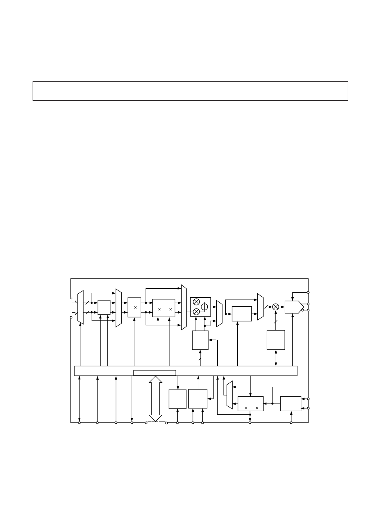
FUNCTIONAL BLOCK DIAGRAM
M
U
X
14
8
14-BIT
DAC
DAC_RSET
IOUT
IOUT
OUTPUT
SCALE
VALUE
DAC CLOCK
REFCLK
REFCLK
MODE
CONTROL
PLL
LOCK
CLOCK
INPUT
MODE
AD9857
PARALLEL
DATA IN
(14-BIT)
D
E
M
U
X
PDCLK/
FUD
14
INVERSE
CIC FILTER
INV
CIC
Q
M
U
X
(4
)
CIC
(2
– 63 )
FIXED
INTER-
POLATOR
PROGRAMMABLE
INTERPOLATOR
M
U
X
QUADRATURE
MODULATOR
SIN
COS
M
U
X
INVERSE
SINC
FILTER
INVERSE
SINC CLOCK
CLOCK
32
TUNING
WORD
TIMING & CONTROL
DDS
CORE
INTERP CLOCK
INTERP CONTROL
HALF-BAND CLOCKS
INVERSE CIC CONTROL
INVERSE CIC CLOCK
DATA CLOCK
CLOCK
MULTIPLIER
(4
– 20 )
M
U
X
PROFILE
SELECT
LOGIC
POWER-
DOWN
LOGIC
CONTROL REGISTERS
RESET
CIC
OVERFLOW
TxENABLE SERIAL
PORT
DIGITAL
POWER-
DOWN
PS1 PS0
SYNCH
SYSCLK
I
14

REV. B
AD9857
–2–
FEATURES . . . . . . . . . . . . . . . . . . . . . . . . . . . . . . . . . . . . . 1
APPLICATIONS . . . . . . . . . . . . . . . . . . . . . . . . . . . . . . . . . 1
GENERAL DESCRIPTION . . . . . . . . . . . . . . . . . . . . . . . . . 1
FUNCTIONAL BLOCK DIAGRAM . . . . . . . . . . . . . . . . . 1
SPECIFICATIONS . . . . . . . . . . . . . . . . . . . . . . . . . . . . . . . 3
ABSOLUTE MAXIMUM RATINGS . . . . . . . . . . . . . . . . . 5
ORDERING GUIDE . . . . . . . . . . . . . . . . . . . . . . . . . . . . . . 5
EXPLANATION OF TEST LEVELS . . . . . . . . . . . . . . . . . 5
PIN CONFIGURATION . . . . . . . . . . . . . . . . . . . . . . . . . . . 5
PIN FUNCTION DESCRIPTIONS . . . . . . . . . . . . . . . . . . 6
TYPICAL PERFORMANCE CHARACTERISTICS . . . . . 7
Modulated Output Spectral Plots . . . . . . . . . . . . . . . . . . . . 7
Single-Tone Output Spectral Plots . . . . . . . . . . . . . . . . . . . 8
Narrowband SFDR Spectral Plots . . . . . . . . . . . . . . . . . . . 9
Output Constellations . . . . . . . . . . . . . . . . . . . . . . . . . . . 10
MODES OF OPERATION . . . . . . . . . . . . . . . . . . . . . . . . 11
Quadrature Modulation Mode . . . . . . . . . . . . . . . . . . . . . 11
Single-Tone Mode . . . . . . . . . . . . . . . . . . . . . . . . . . . . . . 12
Interpolating DAC Mode . . . . . . . . . . . . . . . . . . . . . . . . . 13
SIGNAL PROCESSING PATH . . . . . . . . . . . . . . . . . . . . . 13
Input Data Assembler . . . . . . . . . . . . . . . . . . . . . . . . . . . 13
Inverse CIC Filter . . . . . . . . . . . . . . . . . . . . . . . . . . . . . . 15
Fixed Interpolator (4¥) . . . . . . . . . . . . . . . . . . . . . . . . . . 15
Programmable (2¥–63¥) CIC Interpolating Filter . . . . . . 16
Quadrature Modulator . . . . . . . . . . . . . . . . . . . . . . . . . . . 17
DDS Core . . . . . . . . . . . . . . . . . . . . . . . . . . . . . . . . . . . . 17
Inverse SINC Filter . . . . . . . . . . . . . . . . . . . . . . . . . . . . . 17
Output Scale Multiplier . . . . . . . . . . . . . . . . . . . . . . . . . . 17
14-Bit D/A Converter . . . . . . . . . . . . . . . . . . . . . . . . . . . 17
Reference Clock Multiplier . . . . . . . . . . . . . . . . . . . . . . . 18
INPUT DATA PROGRAMMING . . . . . . . . . . . . . . . . . . . 18
Control Interface—Serial I/O . . . . . . . . . . . . . . . . . . . . . . 18
General Operation of the Serial Interface . . . . . . . . . . . . . 18
Instruction Byte . . . . . . . . . . . . . . . . . . . . . . . . . . . . . . . . 21
SERIAL INTERFACE PORT PIN DESCRIPTIONS . . . . 21
SCLK . . . . . . . . . . . . . . . . . . . . . . . . . . . . . . . . . . . . . . . 21
CS . . . . . . . . . . . . . . . . . . . . . . . . . . . . . . . . . . . . . . . . . . 21
SDIO . . . . . . . . . . . . . . . . . . . . . . . . . . . . . . . . . . . . . . . . 21
SDO . . . . . . . . . . . . . . . . . . . . . . . . . . . . . . . . . . . . . . . . . 21
SYNCIO . . . . . . . . . . . . . . . . . . . . . . . . . . . . . . . . . . . . . 21
MSB/LSB Transfers . . . . . . . . . . . . . . . . . . . . . . . . . . . . . 21
Notes Serial Port Operation . . . . . . . . . . . . . . . . . . . . . . . 21
CONTROL REGISTER DESCRIPTION . . . . . . . . . . . . . 22
PROFILE #0 . . . . . . . . . . . . . . . . . . . . . . . . . . . . . . . . . . 22
PROFILE #1 . . . . . . . . . . . . . . . . . . . . . . . . . . . . . . . . . . 22
PROFILE #2 . . . . . . . . . . . . . . . . . . . . . . . . . . . . . . . . . . 23
PROFILE #3 . . . . . . . . . . . . . . . . . . . . . . . . . . . . . . . . . . 23
Latency . . . . . . . . . . . . . . . . . . . . . . . . . . . . . . . . . . . . . . 25
Latency for the Single-Tone Mode . . . . . . . . . . . . . . . . . 25
Other Factors Affecting Latency . . . . . . . . . . . . . . . . . . . 25
EASE OF USE FEATURES . . . . . . . . . . . . . . . . . . . . . . . . 27
Profile Select . . . . . . . . . . . . . . . . . . . . . . . . . . . . . . . . . . 27
Setting the Phase of the DDS . . . . . . . . . . . . . . . . . . . . . . 27
Reference Clock Multiplier . . . . . . . . . . . . . . . . . . . . . . . 27
PLL Lock . . . . . . . . . . . . . . . . . . . . . . . . . . . . . . . . . . . . . 27
Single or Differential Clock . . . . . . . . . . . . . . . . . . . . . . . 27
CIC Overflow Pin . . . . . . . . . . . . . . . . . . . . . . . . . . . . . . 28
Clearing the CIC Filter . . . . . . . . . . . . . . . . . . . . . . . . . . 28
Digital Power-Down . . . . . . . . . . . . . . . . . . . . . . . . . . . . 28
Hardware-Controlled Digital Power-Down . . . . . . . . . . . 28
Software-Controlled Digital Power-Down . . . . . . . . . . . . 28
Full Sleep Mode . . . . . . . . . . . . . . . . . . . . . . . . . . . . . . . . 28
Power Management Considerations . . . . . . . . . . . . . . . . . 29
Equivalent I/O Circuits . . . . . . . . . . . . . . . . . . . . . . . . . . 29
OUTLINE DIMENSIONS . . . . . . . . . . . . . . . . . . . . . . . . . 32
Revision History . . . . . . . . . . . . . . . . . . . . . . . . . . . . . . . . . 32
TABLE OF CONTENTS

REV. B
–3–
AD9857
SPECIFICATIONS
Test
Parameter Temp Level Min Typ Max Unit
REF CLOCK INPUT CHARACTERISTICS
Frequency Range
REFCLK Multiplier Disabled Full VI 1 200 MHz
REFCLK Multiplier Enabled at 4× Full VI 1 50 MHz
REFCLK Multiplier Enabled at 20× Full VI 1 10 MHz
Input Capacitance 25°CV 3 pF
Input Impedance 25°C V 100 MΩ
Duty Cycle 25°CV 50 %
Duty Cycle with REFCLK Multiplier Enabled 25°C V 35 65 %
Differential Input (VDD/2) ±200 mV 25°C V 1.45 1.85 V
DAC OUTPUT CHARACTERISTICS
Resolution 14 Bits
Full-Scale Output Current 5 10 20 mA
Gain Error 25°C I 8.5 0 % FS
Output Offset 25°CI 2 µA
Differential Nonlinearity 25°C V 1.6 LSB
Integral Nonlinearity 25°C V 2 LSB
Output Capacitance 25°CV 5 pF
Residual Phase Noise @ 1 kHz Offset, 40 MHz A
OUT
REFCLK Multiplier Enabled at 20× 25°C V –107 dBc/Hz
REFCLK Multiplier at 4× 25°C V –123 dBc/Hz
REFCLK Multiplier Disabled 25°C V –145 dBc/Hz
Voltage Compliance Range 25°C I –0.5 +1.0 V
Wideband SFDR
1 MHz–20 MHz Analog Out 25°C V –75 dBc
20 MHz–40 MHz Analog Out 25°C V –65 dBc
40 MHz–60 MHz Analog Out 25°C V –62 dBc
60 MHz–80 MHz Analog Out 25°C V –60 dBc
Narrowband SFDR
10 MHz Analog Out (±1 MHz) 25°C V –87 dBc
10 MHz Analog Out (±250 kHz) 25°C V –88 dBc
10 MHz Analog Out (±50 kHz) 25°C V –92 dBc
10 MHz Analog Out (±10 kHz) 25°C V –94 dBc
65 MHz Analog Out (±1 MHz) 25°C V –86 dBc
65 MHz Analog Out (±250 kHz) 25°C V –86 dBc
65 MHz Analog Out (±50 kHz) 25°C V –86 dBc
65 MHz Analog Out (±10 kHz) 25°C V –88 dBc
80 MHz Analog Out (±1 MHz) 25°C V –85 dBc
80 MHz Analog Out (±250 kHz) 25°C V –85 dBc
80 MHz Analog Out (±50 kHz) 25°C V –85 dBc
80 MHz Analog Out (±10 kHz) 25°C V –86 dBc
MODULATOR CHARACTERISTICS (65 MHz A
OUT
)
(Input Data: 2.5 MS/s, QPSK, 4× Oversampled,
INV SINC ON, INV CIC ON)
I/Q Offset 25°CIV5565 dB
Error Vector Magnitude 25°C IV 0.4 1 %
INVERSE SINC FILTER (Variation in Gain from
DC to 80 MHz, Inverse SINC Filter ON) 25°CV ±0.1 dB
(VS = 3.3 V ⴞ 5%, R
SET
= 1.96 k⍀, External reference clock frequency = 10 MHz with REFCLK Multiplier
enabled at 20ⴛ).

REV. B
–4–
AD9857–SPECIFICATIONS
Test
Parameter Temp Level Min Typ Max Unit
SPURIOUS POWER (Off Channel, Measured in
Equivalent Bandwidth), Full-Scale Output
6.4 MHz Bandwidth 25°C IV –65 dBc
3.2 MHz Bandwidth 25°C IV –67 dBc
1.6 MHz Bandwidth 25°C IV –69 dBc
0.8 MHz Bandwidth 25°C IV –69 dBc
0.4 MHz Bandwidth 25°C IV –70 dBc
0.2 MHz Bandwidth 25°C IV –72 dBc
SPURIOUS POWER (Off Channel, Measured in
Equivalent Bandwidth), Output Attenuated 18 dB
Relative to Full Scale
6.4 MHz Bandwidth 25°C IV –51 dBc
3.2 MHz Bandwidth 25°C IV –54 dBc
1.6 MHz Bandwidth 25°C IV –56 dBc
0.8 MHz Bandwidth 25°C IV –59 dBc
0.4 MHz Bandwidth 25°C IV –62 dBc
0.2 MHz Bandwidth 25°C IV –63 dBc
TIMING CHARACTERISTICS
Serial Control Bus
Maximum Frequency 25°C I 10 MHz
Minimum Clock Pulsewidth Low (t
PWL
)25°CI 30 ns
Minimum Clock Pulsewidth High (t
PWH
)25°CI 30 ns
Maximum Clock Rise/Fall Time 25°CI 1 ms
Minimum Data Setup Time (t
DS
)25°CI 30 ns
Minimum Data Hold Time (t
DH
)25°CI 0 ns
Maximum Data Valid Time (t
DV
)25°CI 35 ns
Wake-Up Time
1
25°CI 1 ms
Minimum RESET Pulsewidth High (t
RH
)25°C I 5 SYSCLK2 Cycles
Minimum CS Setup Time 25°CI 40 ns
CMOS LOGIC INPUTS
Logic “1” Voltage 25°C IV 2.0 V
Logic “0” Voltage 25°C IV 0.8 V
Logic “1” Current 25°CI 5 µA
Logic “0” Current 25°CI 5 µA
Input Capacitance 25°CV 3 pF
CMOS LOGIC OUTPUTS (1 mA LOAD)
Logic “1” Voltage 25°C I 2.7 V
Logic “0” Voltage 25°C I 0.4 V
POWER SUPPLY V
S
CURRENT3 (All Power Specs
at V
DD
= 3.3 V, 25°C, REFCLK = 200 MHz)
Full Operating Conditions 25°C I 540 615 mA
160 MHz Clock (×16) 25°C I 445 515 mA
120 MHz Clock (×12) 25°C I 345 400 mA
Burst Operation (25%) 25°C I 395 450 mA
Single-Tone Mode 25°C I 265 310 mA
Power-Down Mode 25°C I 71 80 mA
Full-Sleep Mode 25°CI 8 13.5mA
NOTES
1
Wake-Up Time refers to recovery from Full-Sleep Mode. The longest time required is for the Reference Clock Multiplier PLL to lock up (if it is being used). The
Wake-Up Time assumes that there is no capacitor on DAC_BP, and that the recommended PLL loop filter values are used. The state of the Reference Clock Multiplier lock can be determined by observing the signal on the PLL_LOCK pin.
2
SYSCLK refers to the actual clock frequency used on-chip by the AD9857. If the Reference Clock Multiplier is used to multiply the external reference frequency, the
SYSCLK frequency is the external frequency multiplied by the Reference Clock Multiplier multiplication factor. If the Reference Clock Multiplier is not used, the
SYSCLK frequency is the same as the external REFCLK frequency.
3
CIC = 2, INV SINC ON, FTW = 40%, PLL OFF, Auto Power-Down Between Burst On, TxENABLE Duty Cycle = 25%.
Specifications subject to change without notice.
REV. B
AD9857
–5–
CAUTION
ESD (electrostatic discharge) sensitive device. Electrostatic charges as high as 4000 V readily
accumulate on the human body and test equipment and can discharge without detection. Although
the AD9857 features proprietary ESD protection circuitry, permanent damage may occur on
devices subjected to high-energy electrostatic discharges. Therefore, proper ESD precautions are
recommended to avoid performance degradation or loss of functionality.
WARNING!
ESD SENSITIVE DEVICE
ABSOLUTE MAXIMUM RATINGS*
Maximum Junction Temperature . . . . . . . . . . . . . . . . . 150°C
V
S
. . . . . . . . . . . . . . . . . . . . . . . . . . . . . . . . . . . . . . . . . . . 4 V
Digital Input Voltage . . . . . . . . . . . . . . . . . . . . . –0.7 V to +V
S
Digital Output Current . . . . . . . . . . . . . . . . . . . . . . . . . 5 mA
Storage Temperature . . . . . . . . . . . . . . . . . . –65°C to +150°C
Operating Temperature . . . . . . . . . . . . . . . . . –40°C to +85°C
Lead Temperature (Soldering 10 sec) . . . . . . . . . . . . . . 300°C
θ
JA
. . . . . . . . . . . . . . . . . . . . . . . . . . . . . . . . . . . . . . . 35°C/W
θ
JC
. . . . . . . . . . . . . . . . . . . . . . . . . . . . . . . . . . . . . . . 16°C/W
*Absolute maximum ratings are limiting values, to be applied individually, and
beyond which the serviceability of the circuit may be impaired. Functional
operability under any of these conditions is not necessarily implied. Exposure of
absolute maximum rating conditions for extended periods of time may affect
device reliability.
ORDERING GUIDE
Temperature Package Package
Model Range Description Option
AD9857AST –40°C to +85°C Quad Flatpack ST-80
AD9857/PCB 25°C Evaluation Board
EXPLANATION OF TEST LEVELS
Test Level
I. 100% production tested.
II. 100% production tested at 25°C and sample tested at spe-
cific temperatures.
III. Sample tested only.
IV. Parameter is guaranteed by design and characterization
testing.
V. Parameter is a typical value only.
VI. Devices are 100% production tested at 25°C and guaran-
teed by design and characterization testing for industrial
operating temperature range.
PIN CONFIGURATION
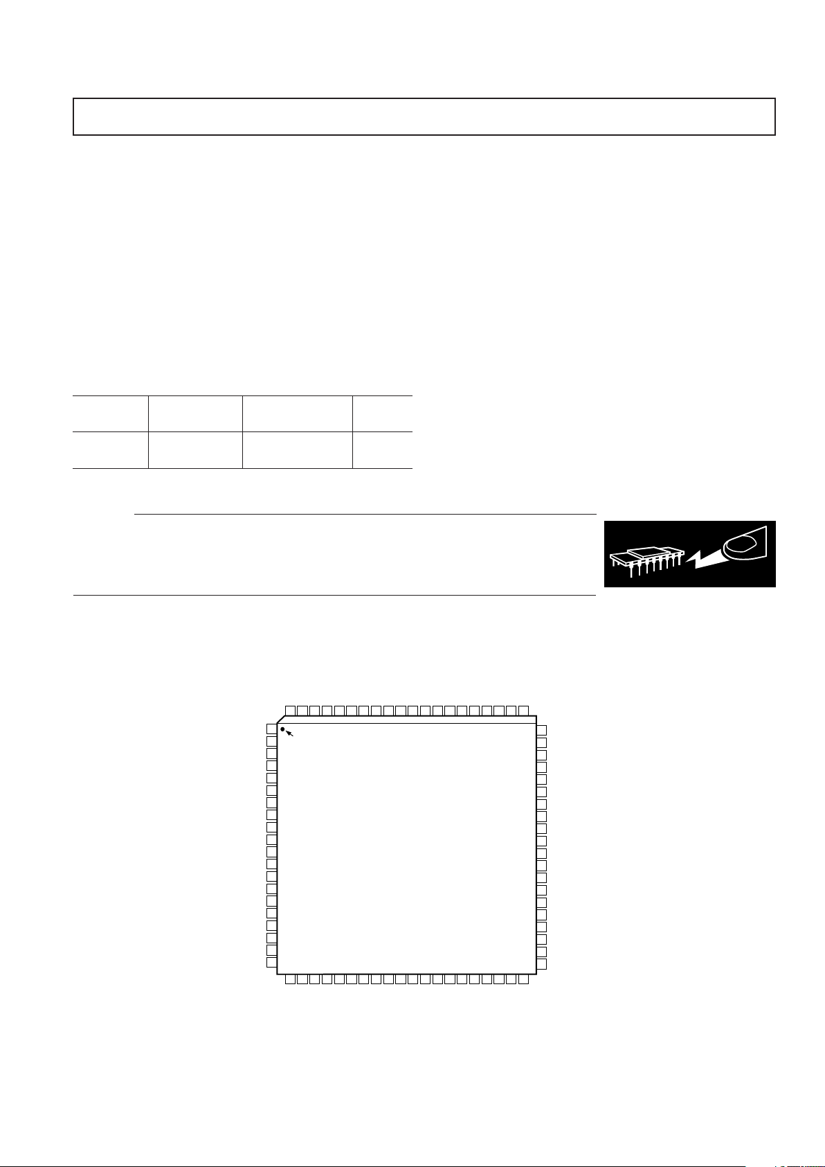
807978 77 76 71 70 69 68 67 66 6575 74 73 72 64 63 62 61
1
2
3
4
5
6
7
8
9
10
11
13
14
15
16
12
17
18
20
19
21 22 23 24 25 26 27 28 29 30 31 32 33 34 35 36 37 38 39 40
PIN 1
IDENTIFIER
TOP VIEW
(Not to Scale)
60
59
58
57
56
55
54
53
52
51
50
49
48
47
46
45
44
43
42
41
NC = NO CONNECT
AD9857
DIFFCLKEN
AGND
AVDD
NC
AGND
PLL_FILTER
AVDD
AGND
NC
NC
DAC_RSET
DAC_BP
AVDD
AGND
IOUT
IOUT
AGND
AVDD
AGND
NC
D13
D12
D11
D10
D9
D8
D7
DVDD
DVDD
DVDD
DGND
DGND
DGND
D6
D5
D4
D3
D2
D1
D0
TxENABLE
PDCLK/FUD
DGND
DGND
DGND
DVDD
DVDD
DVDD
DGND
DGND
DGND
CIC_OVRFL
PLL_LOCK
RESET
DPD
AGND
AVDD
REFCLK
REFCLK
AGND
PS1
PS0
CS
SCLK
SDIO
SDO
SYNCIO
DGND
DGND
DGND
DVDD
DVDD
DVDDNCAVDD
AGND
AVDD
AVDD
AGND
AGND

REV. B
AD9857
–6–
PIN FUNCTION DESCRIPTIONS
Pin Number Mnemonic I/O Pin Function
20–14, 7–1 D0–D6, D7–D13 I 14-Bit Parallel Data Bus for I and Q Data. The required numeric format is two’s
complement with D13 as the sign bit and D12–D0 as the magnitude bits.
Alternating 14-bit words are demultiplexed onto the I and Q data pathways
(except when operating in the Interpolating DAC Mode, in which case every
word is routed onto the I data path). When the TxENABLE pin is asserted high,
the next accepted word is presumed to be I data, the next Q data, and so forth.
8–10, 31–33, 73–75 DVDD 3.3 V Digital Power Pin(s)
11–13, 28–30, 70–72, DGND Digital Ground Pin(s)
76–78
21 PS1 I Profile Select Pin 1. The LSB of the two profile select pins. In conjunction
with PS0, selects one of four profile configurations.
22 PS0 I Profile Select Pin 0. The MSB of the two profile select pins. In conjunction
with P1, selects one of four profile configurations.
23 CS I Serial Port Chip Select Pin. An active low signal that allows multiple devices
to operate on a single serial bus.
24 SCLK I Serial Port Data Clock Pin. The serial data CLOCK for the Serial Port.
25 SDIO I/O Serial Port Input/Output Data Pin. Bidirectional serial DATA pin for the Serial
Port. This pin can be programmed to operate as a serial input only pin, via a
control register bit 00h<7>. The default state is bidirectional.
26 SDO O Serial Port Output Data Pin. This pin serves as the serial data output pin when the
SDIO pin is configured for serial input only mode. The default state is three-state.
27 SYNCIO I Serial Port Synchronization Pin. Synchronizes the serial port without affecting
the programmable register contents. This is an active high input that aborts
the current serial communication cycle.
34, 41, 51, 52, 57 NC No Connect
35, 37, 38, 43, 48, AVDD 3.3 V Analog Power Pin(s)
54, 58, 64
36, 39, 40, 42, 44, 47, AGND Analog Ground Pin(s)
53, 56, 59, 61, 65
45 IOUT O DAC Output Pin. Normal DAC output current (analog).
46 IOUT O DAC Complementary Output Pin. Complementary DAC output current (analog).
49 DAC_BP DAC Reference Bypass. Normally not used.
50 DAC_RSET I DAC Current Set Pin. Sets DAC reference current.
55 PLL_FILTER O PLL Filter. R-C network for PLL Filter.
60 DIFFCLKEN I Clock Mode Select Pin. A logic high on this pin selects DIFFERENTIAL
REFCLK input mode. A logic low selects the SINGLE-ENDED REFCLK
input mode.
62 REFCLK I Reference Clock Pin. In single-ended Clock Mode, this pin is the Reference
Clock input. In differential Clock Mode, this pin is the positive clock input.
63 REFCLK I Inverted Reference Clock Pin. In differential Clock Mode, this pin is the
negative clock input.
66 DPD I Digital Power-Down Pin. Assertion of this pin shuts down the digital sections of
the device to conserve power. However, if selected, the PLL remains operational.
67 RESET I Hardware RESET Pin. An active high input that forces the device into a
predefined state.
68 PLL_LOCK O PLL Lock Pin. Active high output signifying, in real time, when PLL is in
“lock” state.
69 CIC_OVRFL O CIC Overflow Pin. Activity on this pin indicates that the CIC Filters are in
“overflow” state. This pin is normally “low” unless a CIC overflow occurs.
79 PDCLK/FUD I/O Parallel Data Clock/Frequency Update Pin. When not in Single-Tone Mode, this
pin is an output signal that should be used as a clock to synchronize the acceptance
of the 14-bit parallel data words on Pins D13–D0. In Single-Tone Mode, this pin is
an input signal that synchronizes the transfer of a changed Frequency Tuning Word
(FTW) in the active profile (PSx) to the accumulator (FUD = Frequency Update
signal). When profiles are changed by means of the PS–PS1 pins, the FUD does
not have to be asserted to make the FTW active.
80 TxENABLE I When TxENABLE is asserted, the device processes the data through the I and Q
data pathways; otherwise 0s are internally substituted for the I and Q data entering
the signal path. The first data word accepted when the TxENABLE is asserted
high is treated as I data, the next data word is Q data, and so forth.
REV. B
–7–
Typical Performance Characteristics–AD9857
Modulated Output Spectral Plots
–10
–20
–30
–40
–50
–60
–70
–80
–90
–100
START 0Hz 5MHz/ STOP 50MHz
0
dB
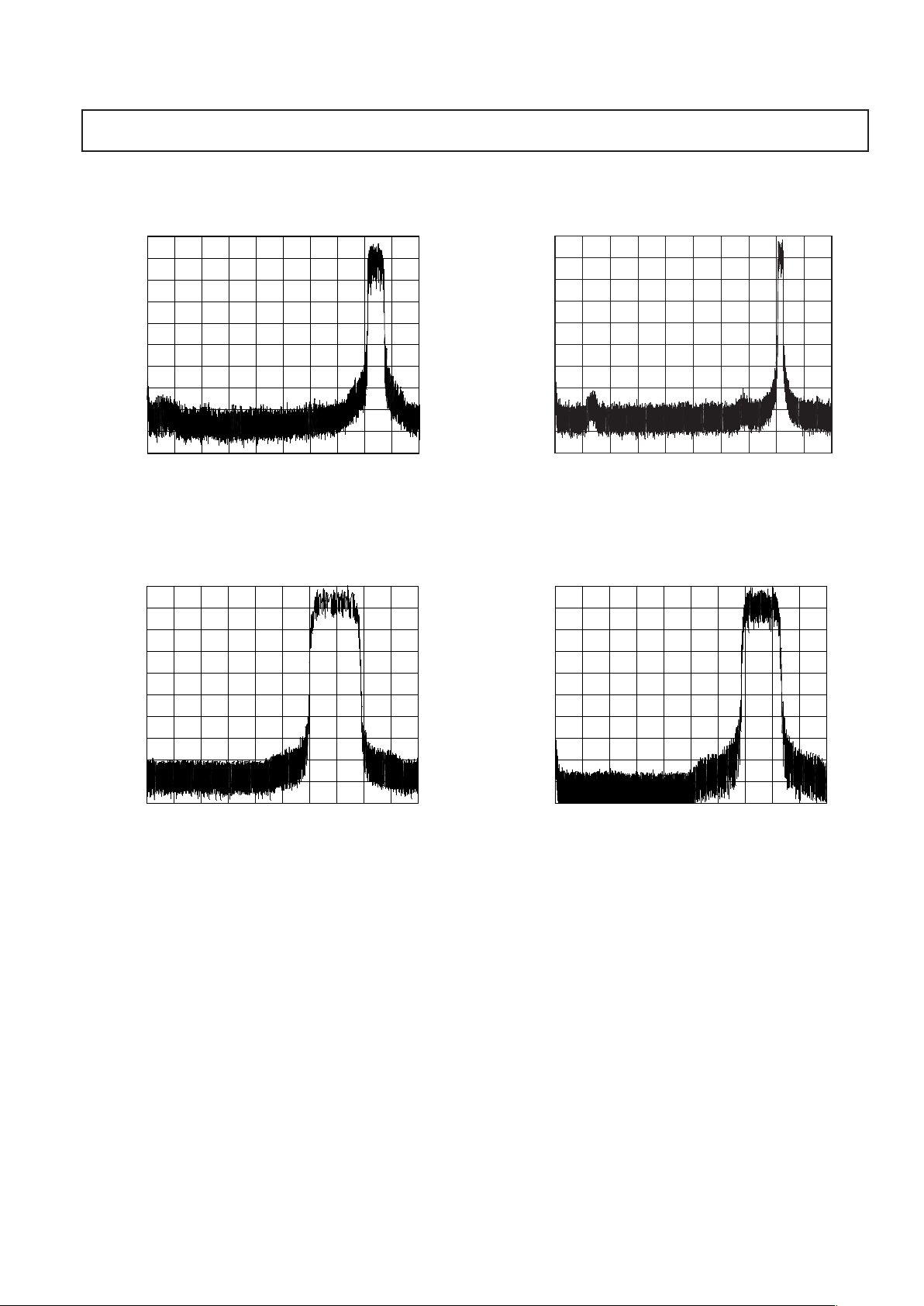
TPC 1. QPSK at 42 MHz and 2.56 MS/s; 10.24 MHz
External Clock with REFCLK Multiplier = 12, CIC
Interpolation Rate = 3, 4
⫻
Oversampled Data
START 0Hz 4MHz/ STOP 40MHz
–8
–16
–24
–32
–40
–48
–56
–64
–72
–80
0
dB
TPC 2. 64-QAM at 28 MHz and 6 MS/s; 36 MHz External
Clock with REFCLK Multiplier = 4, CIC Interpolation
Rate = 2, 3⫻ Oversampled Data
START 0Hz 8MHz/ STOP 80MHz
–10
–20
–30
–40
–50
–60
–70
–80
–90
–100
0
dB
TPC 3. 16-QAM at 65 MHz and 1.28 MS/s; 10.24 MHz
External Clock with REFCLK Multiplier = 18, CIC
Interpolation Rate = 9, 4⫻ Oversampled Data
START 0Hz 5MHz/ STOP 50MHz
–8
–16
–24
–32
–40
–48
–56
–64
–72
–80
0
dB
TP C 4. 256-QAM at 38 MHz and 6 MS/s; 48 MHz External
Clock with REFCLK Multiplier = 4, CIC Interpolation
Rate = 2, 4
⫻
Oversampled Data
REV. B
AD9857
–8–
Single-Tone Output Spectral Plots
START 0Hz 10MHz/ STOP 100MHz
–10
–20
–30
–40
–50
–60
–70
–80
–90
–100
0
dB
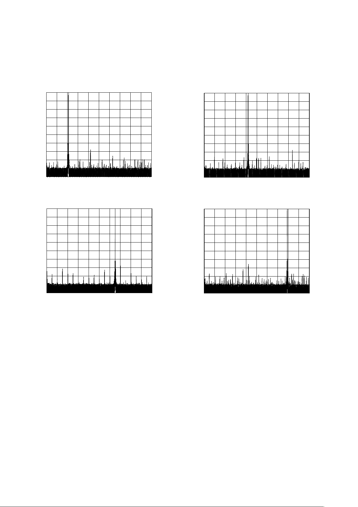
TPC 5. 21 MHz Single-Tone Output
START 0Hz 10MHz/ STOP 100MHz
–10
–20
–30
–40
–50
–60
–70
–80
–90
–100
0
dB
TPC 6. 65 MHz Single-Tone Output
START 0Hz 10MHz/ STOP 100MHz
–10
–20
–30
–40
–50
–60
–70
–80
–90
–100
0
dB
TPC 7. 42 MHz Single-Tone Output
START 0Hz 10MHz/ STOP 100MHz
–10
–20
–30
–40
–50
–60
–70
–80
–90
–100
0
dB
TPC 8. 79 MHz Single-Tone Output
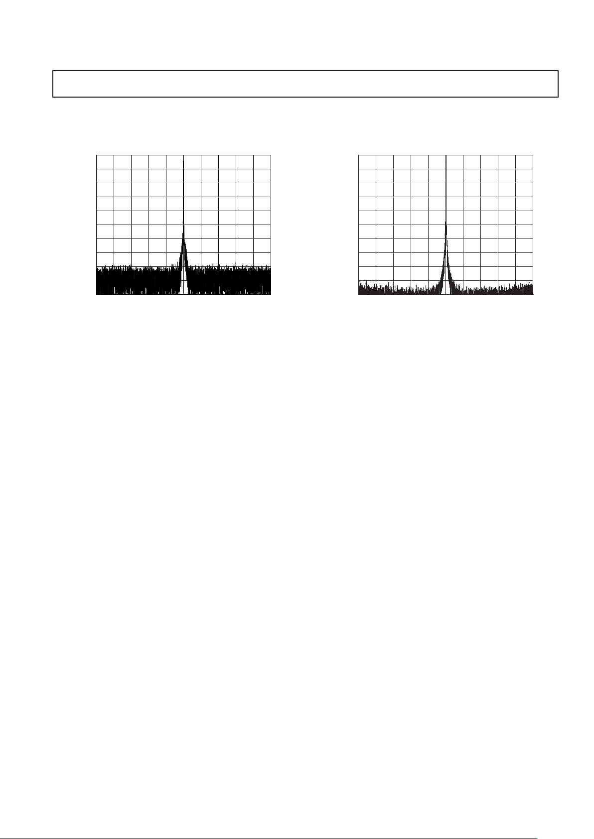
REV. B
AD9857
–9–
Narrowband SFDR Spectral Plots
CENTER 70.1MHz 10kHz/ SPAN 100kHz
–10
–20
–30
–40
–50
–60
–70
–80
–90
–100
0
dB
TPC 9. 70.1 MHz Narrowband SFDR, 10 MHz External
Clock with REFCLK Multiplier = 20
CENTER 70.1MHz 10kHz/ SPAN 100kHz
–10
–20
–30
–40
–50
–60
–70
–80
–90
–100
0
dB
TPC 10. 70.1 MHz Narrowband SFDR, 200 MHz External
Clock with REFCLK Multiplier Disabled
REV. B
AD9857
–10–
–1.3071895838
1.30718958378
CONST
200m/DIV
–1
1
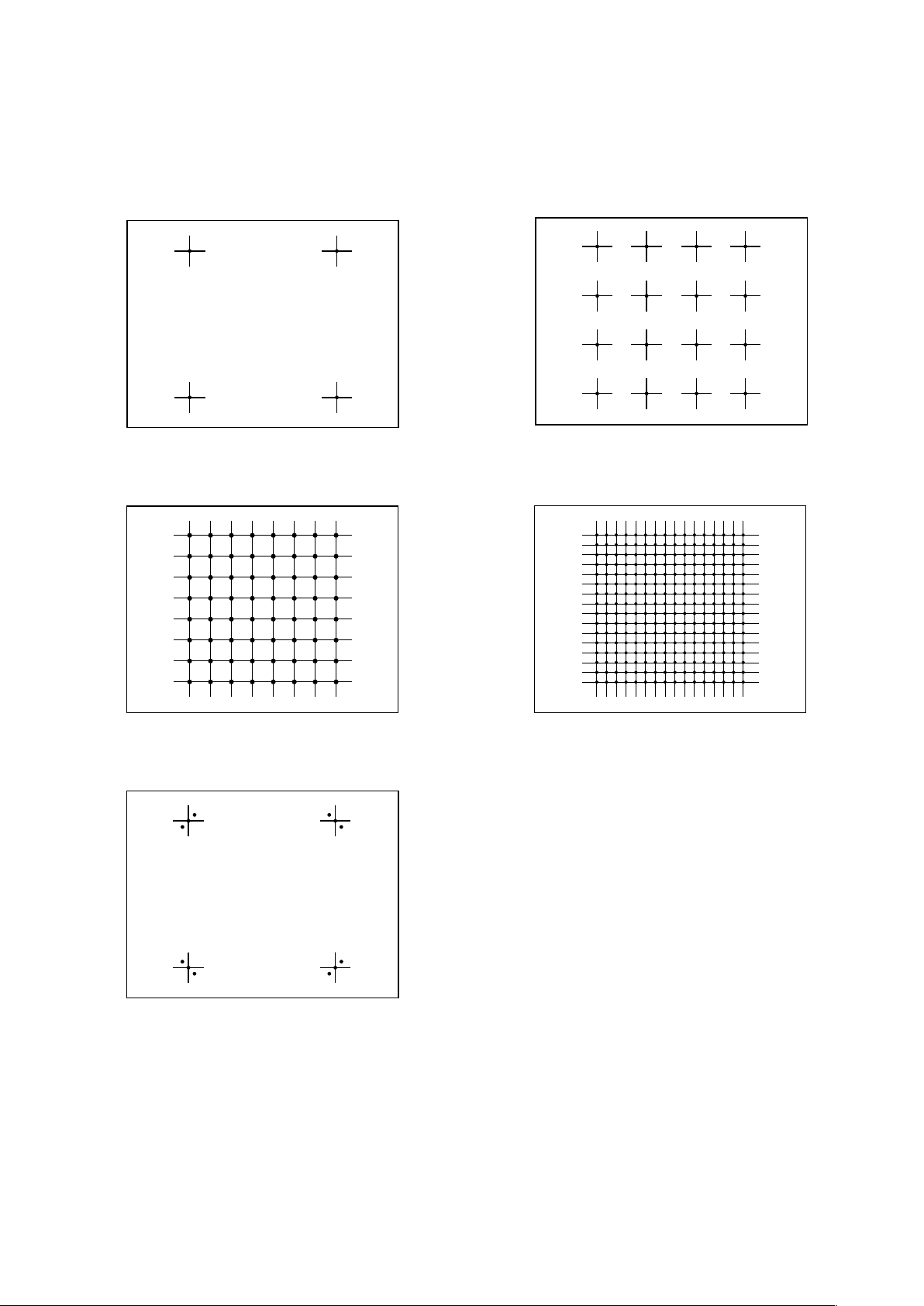
TPC 11. QPSK, 65 MHz, 2.56 MS/s
CONST
200m/DIV
–1
–1.3071895838 1.30718958378
1
TPC 12. 64-QAM, 42 MHz, 6 MS/s
CONST
200m/DIV
–1
–1.3071895838 1.30718958378
1
TPC 13. GMSK Modulation, 13 MS/s
CONST
200m/DIV
–1
–1.3071895838 1.30718958378
1
TPC 14. 16-QAM, 65 MHz, 2.56 MS/s
CONST
200m/DIV
–1
–1.3071895838 1.30718958378
1
TPC 15. 256-QAM, 42 MHz, 6 MS/s
Output Constellations
 Loading...